


 Loading...
Texas Instruments TPS2041BD, TPS2041BDBV, TPS2041BDGN, TPS2042BD, TPS2042BDGN Schematic [ru]
...DRB−8 DGN−8
TPS2041B, TPS2042B TPS2043B, TPS2044B, TPS2051B TPS2052B, TPS2053B, TPS2054B
www.ti.com |
D−8 |
D−16 |
DBV−5 |
SLVS514L |
–JUNE 2010–REVISED JUNE 2011 |
|
|
|
CURRENT-LIMITED, POWER-DISTRIBUTION SWITCHES
Check for Samples: TPS2041B, TPS2042B, TPS2043B, TPS2044B, TPS2051B, TPS2052B, TPS2053B, TPS2054B
FEATURES
•70-mΩ High-Side MOSFET
•500-mA Continuous Current
•Thermal and Short-Circuit Protection
•Accurate Current Limit (0.75 A min, 1.25 A max)
•Operating Range: 2.7 V to 5.5 V
•0.6-ms Typical Rise Time
•Undervoltage Lockout
•Deglitched Fault Report (OC)
•No OC Glitch During Power Up
•Maximum Standby Supply Current:
1-μA (Single, Dual) or 2-μA (Triple, Quad)
•Ambient Temperature Range: -40°C to 85°C
•UL Recognized, File Number E169910
•Additional UL Recognition for TPS2042B and TPS2052B for Ganged Configuration
APPLICATIONS
•Heavy Capacitive Loads
•Short-Circuit Protections
|
TPS2041B/TPS2051B |
|
TPS2041B/TPS2051B |
|
TPS2042B/TPS2052B |
|||||||||||||||||||||||||||||||||
|
|
|
|
DBV PACKAGE |
|
|
D AND DGN PACKAGES |
|
D AND DGN PACKAGES |
|||||||||||||||||||||||||||||
|
|
|
|
|
(TOP VIEW) |
|
|
|
|
|
|
(TOP VIEW) |
|
|
|
|
|
|
|
|
(TOP VIEW) |
|
|
|
||||||||||||||
|
|
|
|
|
|
|
|
|
|
|
|
|
|
|
|
|
|
|
|
|
|
|
|
|
|
|
|
|
|
|
|
|
|
|
||||
OUT |
|
|
|
|
|
|
|
|
|
|
|
|
|
|
|
|
|
|
|
|
|
|
|
|
|
|
|
|
|
|
|
|
|
|
|
|||
|
|
|
|
|
IN |
GND |
|
|
1 |
|
|
8 |
OUT |
|
GND |
|
1 |
|
|
8 |
OC1 |
|||||||||||||||||
GND |
|
|
|
|
|
|
|
|
IN |
|
|
2 |
|
|
7 |
OUT |
|
|
IN |
|
2 |
|
|
7 |
OUT1 |
|||||||||||||
|
|
|
|
|
|
|
|
|
|
|
|
|
|
|
|
|
||||||||||||||||||||||
|
|
|
|
|
|
|
|
|
|
|
|
|
|
|
|
|
|
|
|
|
|
|
|
|
|
|
|
|
|
|
|
|
|
|
||||
|
|
|
|
|
|
|
|
|
|
|
|
IN |
|
|
3 |
|
|
6 |
OUT |
|
EN1† |
|
3 |
|
|
6 |
OUT2 |
|||||||||||
|
|
|
|
|
|
|
|
|
|
|
|
|
|
† |
|
|
|
|
|
|
|
|
|
|
|
|
|
|
|
|
|
|
|
|
|
|
||
|
|
|
|
|
|
|
|
|
|
† |
|
EN |
|
|
4 |
|
|
5 |
OC |
|
|
|
|
† |
|
4 |
|
|
5 |
OC2 |
||||||||
OC |
|
|
|
|
|
|
|
|
|
|
|
|
EN2 |
|
|
|
||||||||||||||||||||||
|
|
|
|
|
EN |
|
|
|
|
|
|
|
|
|
|
|||||||||||||||||||||||
|
|
|
|
|
|
|
|
|
|
|
|
TPS2043B/TPS2053B |
|
TPS2044B/TPS2054B |
||||||||||||||||||||||||
|
|
|
|
|
|
|
|
|
|
|
|
|
||||||||||||||||||||||||||
|
|
|
|
|
|
|
|
|
|
|
|
|
|
|
D PACKAGE |
|
|
|
|
|
|
|
|
D PACKAGE |
|
|
|
|||||||||||
|
|
|
|
|
|
|
|
|
|
|
|
|
|
|
|
(TOP VIEW) |
|
|
|
|
|
|
|
|
(TOP VIEW) |
|
|
|
||||||||||
|
TPS2042B/TPS2052B |
|
|
|
|
|
|
|
|
|
|
|
|
|
|
|
|
|
|
|
|
|
|
|
|
|
|
|
|
|||||||||
|
DRB PACKAGES |
|
|
|
|
|
|
|
|
1 |
|
|
16 |
|
|
|
|
|
|
|
|
1 |
|
|
16 |
|
|
|
||||||||||
|
|
GND |
|
|
|
|
|
OC1 |
GND |
|
|
|
OC1 |
|||||||||||||||||||||||||
|
|
|
|
(TOP VIEW) |
|
|
|
|
|
|
|
|
|
|
||||||||||||||||||||||||
|
|
|
|
|
|
|
|
|
|
|
||||||||||||||||||||||||||||
|
|
|
|
|
|
|
|
|
|
|
|
IN1 |
|
|
2 |
|
|
15 |
|
OUT1 |
|
IN1 |
2 |
|
|
15 |
|
OUT1 |
||||||||||
|
|
|
|
|
|
|
|
|
OC1 |
|
|
|
|
|
|
|
|
|
|
|
|
|
|
|
|
|
|
|
|
|
|
|
|
|
|
|
|
|
GND |
1 |
8 |
|
EN1† |
|
|
3 |
|
|
14 |
|
OUT2 |
EN1† |
3 |
|
|
14 |
|
OUT2 |
|||||||||||||||||||
|
IN |
|
|
|
|
|
OUT1 |
EN2† |
|
|
4 |
|
|
13 |
|
|
|
EN2† |
4 |
|
|
13 |
|
|
|
|||||||||||||
|
|
|
|
|
|
|
|
|
|
|
|
|
|
|
|
|
|
|||||||||||||||||||||
|
2 |
7 |
|
|
|
|
|
|
OC2 |
|
|
|
OC2 |
|||||||||||||||||||||||||
|
|
|
|
|
|
|
|
|
|
|
|
|
|
|
|
|
|
|
|
|
|
|
|
|
|
|
|
|
|
|
|
|
|
|
||||
|
|
† 3 |
|
|
|
|
|
|
|
|
|
|
|
|
5 |
|
|
12 |
|
|
|
|
|
|
|
|
5 |
|
|
12 |
|
|
|
|||||
EN1 |
6 |
|
OUT2 |
GND |
|
|
|
|
|
OC3 |
GND |
|
|
|
OC3 |
|||||||||||||||||||||||
|
|
|
|
|
|
6 |
|
|
11 |
|
6 |
|
|
11 |
||||||||||||||||||||||||
|
|
† 4 |
|
|
|
|
|
|
|
IN2 |
|
|
|
|
|
OUT3 |
|
IN2 |
|
|
|
OUT3 |
||||||||||||||||
|
|
5 |
|
OC2 |
|
|
|
|
|
|
|
|
||||||||||||||||||||||||||
EN2 |
|
|
|
|
|
|
|
|
||||||||||||||||||||||||||||||
|
|
|
|
|
|
|
|
|
|
|
|
|
† |
|
|
7 |
|
|
10 |
|
NC |
|
† |
7 |
|
|
10 |
|
OUT4 |
|||||||||
|
|
|
|
|
|
|
|
|
|
|
EN3 |
|
|
|
|
EN3 |
||||||||||||||||||||||
|
|
|
|
|
|
|
|
|
|
|
|
|
|
|
|
|
|
|
|
|
|
|
|
|
|
|
||||||||||||
|
|
|
|
|
|
|
|
|
|
|
|
|
|
|
|
|
|
|
|
|
|
|
|
|
|
|
|
|
|
|||||||||
|
|
|
|
|
|
|
|
|
|
|
|
NC |
|
|
8 |
|
|
9 |
|
NC |
|
|
† |
8 |
|
|
9 |
|
OC4 |
|||||||||
|
|
|
|
|
|
|
|
|
|
|
|
|
|
|
|
|
EN4 |
|
|
|
||||||||||||||||||
|
|
|
|
|
|
|
|
|
|
|
|
|
|
|
|
|
|
|
|
|
|
|
|
|
|
|
|
|
|
|
||||||||
|
|
|
|
|
|
|
|
|
|
|
|
|
|
|
|
|
|
|
|
|
|
|
|
|
|
|
|
|
|
|
|
|
|
|
|
|
|
|
†
All enable inputs are active high for the TPS205xB series. NC − No connect
DESCRIPTION
The TPS204xB/TPS205xB power-distribution switches are intended for applications where heavy capacitive loads and short circuits are likely to be encountered. These devices incorporates 70-mΩ N-channel MOSFET power switches for power-distribution systems that require multiple power switches in a single package. Each switch is controlled by a logic enable input. Gate drive is provided by an internal charge pump designed to control the power-switch rise times and fall times to minimize current surges during switching. The charge pump requires no external components and allows operation from supplies as low as 2.7 V.
When the output load exceeds the current-limit threshold or a short is present, the device limits the output current to a safe level by switching into a constant-current mode, pulling the overcurrent (OCx) logic output low. When continuous heavy overloads and short-circuits increase the power dissipation in the switch, causing the junction temperature to rise, a thermal protection circuit shuts off the switch to prevent damage. Recovery from a thermal shutdown is automatic once the device has cooled sufficiently. Internal circuitry ensures that the switch remains off until valid input voltage is present. This power-distribution switch is designed to set current limit at 1 A typically.
GENERAL SWITCH CATALOG
33 mΩ, Single
TPS201xA 0.2 A to 2 A TPS202x 0.2 A to 2 A TPS203x 0.2 A to 2 A
80 mΩ, Single |
80 mΩ, Dual |
||||||||||
|
|
|
|
|
|
|
|
|
|
|
|
TPS2014 600 mA |
|
|
|
|
|
|
|||||
|
|
|
|
|
|
||||||
|
|
|
|
|
|
||||||
TPS2015 1 A |
|
|
|
|
|
|
|||||
TPS2041B 500 mA |
TPS2042B 500 mA |
||||||||||
TPS2051B 500 mA |
TPS2052B 500 mA |
||||||||||
TPS2045A |
250 mA |
TPS2046B 250 mA |
|||||||||
TPS2049 100 mA |
TPS2056 250 mA |
||||||||||
TPS2055A |
250 mA |
TPS2062 1 A |
|||||||||
TPS2061 1 A |
TPS2066 1 A |
||||||||||
TPS2065 1 A |
TPS2060 1.5 A |
||||||||||
TPS2068 1.5 A |
TPS2064 1.5 A |
||||||||||
TPS2069 1.5 A |
|
|
|
|
|
|
|||||
|
|
|
|
|
|
|
|
|
|
|
|
80 mΩ, Dual
TPS2080 500 mA TPS2081 500 mA TPS2082 500 mA TPS2090 250 mA TPS2091 250 mA TPS2092 250 mA
80 mΩ, Triple
TPS2043B 500 mA TPS2053B 500 mA TPS2047B 250 mA TPS2057A 250 mA TPS2063 1 A TPS2067 1 A
80 mΩ, Quad
TPS2044B 500 mA TPS2054B 500 mA TPS2048A 250 mA TPS2058 250 mA
80 mΩ, Quad
TPS2085 500 mA TPS2086 500 mA TPS2087 500 mA TPS2095 250 mA TPS2096 250 mA TPS2097 250 mA
See TI Switch Portfolio at http://www.ti.com/usbpower
Please be aware that an important notice concerning availability, standard warranty, and use in critical applications of Texas
Instruments semiconductor products and disclaimers thereto appears at the end of this data sheet.
PowerPAD is a trademark of Texas Instruments.
UNLESS OTHERWISE NOTED this |
document |
contains |
Copyright © 2010–2011, Texas Instruments Incorporated |
PRODUCTION DATA information current as of publication date. |
|
||
Products conform to specifications per |
the terms |
of Texas |
|
Instruments standard warranty. Production processing does not |
|
||
necessarily include testing of all parameters. |
|
|
|

TPS2041B, TPS2042B
TPS2043B, TPS2044B, TPS2051B
TPS2052B, TPS2053B, TPS2054B
SLVS514L –JUNE 2010 –REVISED JUNE 2011 |
www.ti.com |
These devices have limited built-in ESD protection. The leads should be shorted together or the device placed in conductive foam during storage or handling to prevent electrostatic damage to the MOS gates.
DEVICE INFORMATION(1)
|
|
|
TYPICAL |
|
|
PACKAGED DEVICES |
|
||
|
|
RECOMMENDED |
SHORT- |
NUMBER |
|
|
|
|
|
|
|
|
|
|
|
||||
|
|
MAXIMUM |
CIRCUIT |
|
|
|
|
||
TA |
ENABLE |
OF |
|
|
|
|
|||
CONTINUOUS |
CURRENT |
MSOP (DGN) |
SOIC (D) |
SOT-23 (DBV) |
SON (DRB) |
||||
|
|
SWITCHES |
|||||||
|
|
LOAD CURRENT |
LIMIT |
||||||
|
|
|
|
|
|
|
|||
|
|
|
AT 25°C |
|
|
|
|
|
|
|
Active low |
|
|
Single |
TPS2041BDGN |
TPS2041BD |
TPS2041BDBV |
|
|
|
|
|
|
|
|
|
|
|
|
|
Active high |
|
|
Single |
TPS2051BDGN |
TPS2051BD |
TPS2051BDBV |
|
|
|
|
|
|
|
|
|
|
|
|
|
Active low |
|
|
Dual |
TPS2042BDGN |
TPS2042BD |
|
TPS2042BDRB |
|
|
|
|
|
|
|
|
|
|
|
-40°C to |
Active high |
0.5 A |
1 A |
Dual |
TPS2052BDGN |
TPS2052BD |
|
TPS2052BDRB |
|
85°C |
Active low |
Triple |
-- |
TPS2043BD |
|
|
|||
|
|
|
|
||||||
|
|
|
|
|
|
|
|
|
|
|
Active high |
|
|
Triple |
-- |
TPS2053BD |
|
|
|
|
|
|
|
|
|
|
|
|
|
|
Active low |
|
|
Quad |
-- |
TPS2044BD |
|
|
|
|
|
|
|
|
|
|
|
|
|
|
Active high |
|
|
Quad |
-- |
TPS2054BD |
|
|
|
|
|
|
|
|
|
|
|
|
|
(1)For the most current package and ordering information, see the Package Option Addendum at the end of this document, or see the TI website at www.ti.com.
ABSOLUTE MAXIMUM RATINGS
over operating free-air temperature range unless otherwise noted(1)
|
|
|
|
|
|
|
UNIT |
|
|
|
|
||||||
(2) |
|
-0.3 V to 6 V |
||||||
Input voltage range, VI(IN), VI(INx) |
||||||||
(2) |
|
-0.3 V to 6 V |
||||||
Output voltage range, VO(OUT), VO(OUTx) |
||||||||
Input voltage range, VI(EN) |
, V |
|
, VI(EN), VI(ENx) |
-0.3 V to 6 V |
||||
I(ENx) |
||||||||
Voltage range, VI(/OC), V |
|
|
|
|
|
-0.3 V to 6 V |
||
I(OCx) |
||||||||
Continuous output current, IO(OUT), IO(OUTx) |
Internally limited |
|||||||
Continuous total power dissipation |
See Dissipation Rating Table |
|||||||
|
|
|
|
|
|
|
||
Operating virtual junction temperature range, TJ |
-40°C to 125°C |
|||||||
Storage temperature range, Tstg |
-65°C to 150°C |
|||||||
Electrostatic discharge (ESD) protection |
Human body model (HBM) |
2 kV |
||||||
|
|
|||||||
Charge device model (CDM) |
500 V |
|||||||
|
|
|
|
|
|
|||
|
|
|
|
|
|
|
|
|
(1)Stresses beyond those listed under absolute maximum ratings may cause permanent damage to the device. These are stress ratings only, and functional operation of the device at these or any other conditions beyond those indicated under recommended operating conditions is not implied. Exposure to absolute-maximum-rated conditions for extended periods may affect device reliability.
(2)All voltages are with respect to GND.
DISSIPATING RATING TABLE
PACKAGE |
THERMAL |
TA ≤ 25°C |
DERATING FACTOR |
TA = 70°C |
TA = 85°C |
|
RESISTANCE, θJA |
POWER RATING |
ABOVE TA = 25°C |
POWER RATING |
POWER RATING |
||
|
||||||
DGN-8 |
|
1712.3 mW |
17.123 mW/°C |
941.78 mW |
684.93 mW |
|
D-8 |
|
585.82 mW |
5.8582 mW/°C |
322.20 mW |
234.32 mW |
|
D-16 |
|
898.47 mW |
8.9847 mW/°C |
494.15 mW |
359.38 mW |
|
DBV-5 |
|
285 mW |
2.85 mW/°C |
155 mW |
114 mW |
|
DRB-8 (Low-K)(1) |
270 °CW |
370 mW |
3.71 mW/°C |
203 mW |
148 mW |
|
DRB-8 (High-K)(2) |
60 °CW |
1600 mW |
16.67 mW/°C |
916 mW |
866 mW |
(1)Soldered PowerPAD on a standard 2-layer PCB without vias for thermal pad. See TI application note SLMA002 for further details.
(2)Soldered PowerPAD on a standard 4-layer PCB with vias for thermal pad. See TI application note SLMA002 for further details.
2 |
Copyright © 2010–2011, Texas Instruments Incorporated |

TPS2041B, TPS2042B
TPS2043B, TPS2044B, TPS2051B
TPS2052B, TPS2053B, TPS2054B
www.ti.com SLVS514L –JUNE 2010–REVISED JUNE 2011
RECOMMENDED OPERATING CONDITIONS
|
|
|
|
MIN |
MAX |
UNIT |
|
|
|
|
|
||
Input voltage, VI(IN), VI(INx) |
2.7 |
5.5 |
V |
|||
Input voltage, VI(EN) |
, V |
|
, VI(EN), VI(ENx) |
0 |
5.5 |
V |
I(ENx) |
||||||
Continuous output current, IO(OUT), IO(OUTx) |
0 |
500 |
mA |
|||
Operating virtual junction temperature, TJ |
-40 |
125 |
°C |
|||
ELECTRICAL CHARACTERISTICS
over recommended operating junction temperature range, VI(IN) = 5.5 V, IO = 0.5 A, VI(/ENx) = 0 V (unless otherwise noted)
|
PARAMETER |
|
|
|
|
|
TEST CONDITIONS(1) |
MIN |
TYP |
MAX |
UNIT |
|||||||
POWER SWITCH |
|
|
|
|
|
|
|
|
|
|
|
|
|
|||||
|
|
|
|
|
|
|
|
|
|
|||||||||
|
Static drain-source on-state |
V = 5 V or 3.3 V, I |
|
= 0.5 A, |
D and DGN packages |
|
70 |
135 |
|
|||||||||
|
resistance, 5-V operation |
I(IN) |
O |
|
|
|
|
|
|
|
mΩ |
|||||||
|
-40°C ≤ TJ ≤ 125°C |
|
|
|
|
DBV package only |
|
95 |
140 |
|||||||||
|
and 3.3-V operation |
|
|
|
|
|
|
|||||||||||
|
|
|
|
|
|
|
|
|
|
|
|
|
|
|||||
|
|
|
|
|
|
|
|
|||||||||||
rDS(on) |
Static drain-source on-state |
VI(IN) = 2.7 V, IO = 0.5 A, |
D and DGN packages |
|
75 |
150 |
mΩ |
|||||||||||
|
resistance, 2.7-V operation |
-40°C ≤ TJ ≤ 125°C |
|
|
|
|
|
|||||||||||
|
|
|
|
|
|
|
|
|
|
|||||||||
|
Static drain-source on-state |
VI(IN) = 5 V, IO = 1.0 A, OUT1 and OUT2 |
DGN package, |
|
|
49 |
mΩ |
|||||||||||
|
resistance, 5-V operation |
connected, 0°C ≤ TJ ≤ 70°C |
TPS2042B/52B |
|
|
|||||||||||||
|
|
|
|
|
||||||||||||||
tr |
Rise time, output |
VI(IN) = 5.5 V |
|
|
|
|
|
|
0.6 |
1.5 |
|
|||||||
VI(IN) = 2.7 V |
|
CL = 1 μF, |
TJ = 25°C |
|
0.4 |
1 |
ms |
|||||||||||
|
|
|
|
|
|
|
|
|||||||||||
tf |
Fall time, output |
VI(IN) = 5.5 V |
|
RL = 10 Ω |
0.05 |
|
0.5 |
|||||||||||
|
|
|
|
|||||||||||||||
VI(IN) = 2.7 V |
|
|
|
|
|
0.05 |
|
0.5 |
|
|||||||||
|
|
|
|
|
|
|
|
|
|
|
|
|
||||||
ENABLE INPUT |
|
AND |
|
|
|
|
|
|
|
|
|
|
|
|
|
|
|
|
EN |
ENx |
|
|
|
|
|
|
|
|
|
|
|
|
|
||||
VIH |
High-level input voltage |
2.7 V ≤ VI(IN) ≤ 5.5 V |
|
|
|
|
|
2 |
|
|
V |
|||||||
VIL |
Low-level input voltage |
2.7 V ≤ VI(IN) ≤ 5.5 V |
|
|
|
|
|
|
|
0.8 |
||||||||
|
|
|
|
|
|
|
|
|||||||||||
II |
Input current |
V |
|
= 0 V or 5.5 V |
|
|
|
|
|
-0.5 |
|
0.5 |
μA |
|||||
I(ENx) |
|
|
|
|
|
|
||||||||||||
ton |
Turnon time |
CL = 100 μF, RL = 10 Ω |
|
|
|
3 |
ms |
|||||||||||
toff |
Turnoff time |
CL = 100 μF, RL = 10 Ω |
|
|
|
10 |
||||||||||||
|
|
|
|
|||||||||||||||
CURRENT LIMIT |
|
|
|
|
|
|
|
|
|
|
|
|
|
|||||
|
|
|
|
|
|
|
|
|
|
|
|
|
|
|
||||
|
|
|
|
|
|
V = 5 V, OUT connected to GND, |
TJ = 25°C |
0.75 |
1 |
1.25 |
|
|||||||
|
|
|
|
|
|
I(IN) |
|
|
|
|
|
|
|
|
|
|||
IOS |
Short-circuit output current |
device enabled into short-circuit |
-40°C ≤ TJ ≤ 125°C |
0.7 |
1 |
1.3 |
A |
|||||||||||
VI(IN) = 5 V, OUT1 and OUT2 connected to |
0°C ≤ TJ ≤ 70°C |
|
|
|
||||||||||||||
|
|
|
|
|
|
GND, device enabled into short-circuit, |
1.5 |
|
|
|
||||||||
|
|
|
|
|
|
TPS2042B/52B |
|
|
|
|||||||||
|
|
|
|
|
|
measure at IN |
|
|
|
|
|
|
|
|
||||
|
|
|
|
|
|
|
|
|
|
|
|
|
|
|
||||
|
|
|
|
|
|
|
|
|
|
|
|
|
|
|
|
|
||
IOC |
Overcurrent trip threshold |
VIN = 5 V, 100 A/s |
|
TPS2041B/51B |
|
IOS |
1.5 |
1.9 |
A |
|||||||||
|
TPS2042B/52B |
|
IOS |
1.55 |
2.0 |
|||||||||||||
|
|
|
|
|
|
|
|
|
|
|
|
|
||||||
SUPPLY CURRENT (TPS2041B, TPS2051B) |
|
|
|
|
|
|
|
|
|
|||||||||
|
|
|
|
|
|
|
|
|
|
|
|
|
|
|
|
|
|
|
|
|
|
|
|
|
No load on OUT, V |
|
|
= 5.5 V, |
TJ = 25°C |
|
0.5 |
1 |
|
||||
Supply current, low-level output |
I(ENx) |
|
μA |
|||||||||||||||
or VI(ENx) = 0 V |
|
|
|
|
-40°°C ≤ TJ ≤ 125°C |
|
0.5 |
5 |
||||||||||
|
|
|
|
|
|
|
|
|
|
|
|
|||||||
|
|
|
|
|
|
No load on OUT, V |
|
|
= 0 V, |
TJ = 25°C |
|
43 |
60 |
|
||||
Supply current, high-level output |
I(ENx) |
|
μA |
|||||||||||||||
or VI(ENx) = 5.5 V |
|
|
|
|
-40°C ≤ TJ ≤ 125°C |
|
43 |
70 |
||||||||||
|
|
|
|
|
|
|
|
|
|
|
|
|||||||
|
|
|
|
|
|
OUT connected to ground, V |
|
= 5.5 V, |
|
|
|
|
|
|||||
Leakage current |
I(ENx) |
-40°C ≤ TJ ≤ 125°C |
|
1 |
|
μA |
||||||||||||
or VI(ENx) = 0 V |
|
|
|
|
|
|
||||||||||||
|
|
|
|
|
|
|
|
|
|
|
|
|
|
|
||||
Reverse leakage current |
VI(OUTx) = 5.5 V, IN = ground |
TJ = 25°C |
|
0 |
|
μA |
||||||||||||
(1)Pulse-testing techniques maintain junction temperature close to ambient temperature; thermal effects must be taken into account separately.
Copyright © 2010–2011, Texas Instruments Incorporated |
3 |

TPS2041B, TPS2042B
TPS2043B, TPS2044B, TPS2051B
TPS2052B, TPS2053B, TPS2054B
SLVS514L –JUNE 2010 –REVISED JUNE 2011 |
www.ti.com |
ELECTRICAL CHARACTERISTICS (continued)
over recommended operating junction temperature range, VI(IN) = 5.5 V, IO = 0.5 A, VI(/ENx) = 0 V (unless otherwise noted)
|
|
PARAMETER |
|
|
|
|
|
|
|
TEST CONDITIONS(1) |
MIN |
TYP |
MAX |
UNIT |
|||||||
|
SUPPLY CURRENT (TPS2042B, TPS2052B) |
|
|
|
|
|
|
|
|
||||||||||||
|
|
|
|
|
|
|
|
|
|
|
|
|
|
|
|
|
|
|
|
|
|
|
Supply current, low-level output |
|
No load on OUT, V |
|
= 5.5 V |
TJ = 25°C |
|
0.5 |
1 |
μA |
|||||||||||
|
|
I(ENx) |
-40°C ≤ TJ ≤ 125°C |
|
0.5 |
5 |
|||||||||||||||
|
|
|
|
|
|
|
|
|
|
|
|
|
|
|
|
|
|
|
|||
|
Supply current, high-level output |
|
No load on OUT, V |
|
= 0 V |
TJ = 25°C |
|
50 |
70 |
μA |
|||||||||||
|
|
I(ENx) |
-40°C ≤ TJ ≤ 125°C |
|
50 |
90 |
|||||||||||||||
|
|
|
|
|
|
|
|
|
|
|
|
|
|
|
|
|
|
|
|||
|
Leakage current |
|
OUT connected to ground, V |
|
= 5.5 V |
-40°C ≤ TJ ≤ 125°C |
|
1 |
|
μA |
|||||||||||
|
|
I(ENx) |
|
|
|||||||||||||||||
|
Reverse leakage current |
|
VI(OUTx) = 5.5 V, IN = ground |
TJ = 25°C |
|
0.2 |
|
μA |
|||||||||||||
|
SUPPLY CURRENT (TPS2043B, TPS2053B) |
|
|
|
|
|
|
|
|
||||||||||||
|
|
|
|
|
|
|
|
|
|
|
|
|
|
|
|
|
|
|
|
|
|
|
Supply current, low-level output |
|
No load on OUT, VI(ENx) = 0 V |
TJ = 25°C |
|
0.5 |
2 |
μA |
|||||||||||||
|
|
-40°C ≤ TJ ≤ 125°C |
|
0.5 |
10 |
||||||||||||||||
|
|
|
|
|
|
|
|
|
|
|
|
|
|
|
|
|
|
|
|||
|
Supply current, high-level output |
|
No load on OUT, VI(ENx) = 5.5 V |
TJ = 25°C |
|
65 |
90 |
μA |
|||||||||||||
|
|
-40°C ≤ TJ ≤ 125°C |
|
65 |
110 |
||||||||||||||||
|
|
|
|
|
|
|
|
|
|
|
|
|
|
|
|
|
|
|
|||
|
Leakage current |
|
OUT connected to ground, VI(ENx) = 0 V |
-40°C≤ TJ ≤ 125°C |
|
1 |
|
μA |
|||||||||||||
|
Reverse leakage current |
|
VI(OUTx) = 5.5 V, INx = ground |
TJ = 25°C |
|
0.2 |
|
μA |
|||||||||||||
|
SUPPLY CURRENT (TPS2044B, TPS2054B) |
|
|
|
|
|
|
|
|
||||||||||||
|
|
|
|
|
|
|
|
|
|
|
|
|
|
|
|
|
|
|
|||
|
|
|
|
|
|
|
|
No load on OUT, V |
|
|
= 5.5 V, |
TJ = 25°C |
|
0.5 |
2 |
|
|||||
|
|
|
|
|
|
|
|
|
|
|
|||||||||||
|
Supply current, low-level output |
|
|
|
|
I(ENx) |
|
|
|
|
|
|
|
μA |
|||||||
|
|
or VI(ENx) = 0 V |
|
|
|
-40°C ≤ TJ ≤ 125°C |
|
0.5 |
10 |
||||||||||||
|
|
|
|
|
|
|
|
|
|
|
|
|
|||||||||
|
|
|
|
|
|
|
|
No load on OUT, V |
|
|
= 0 V, |
TJ = 25°C |
|
75 |
110 |
|
|||||
|
|
|
|
|
|
|
|
|
|
|
|||||||||||
|
Supply current, high-level output |
|
|
|
|
I(ENx) |
|
|
|
|
|
|
|
μA |
|||||||
|
|
or VI(ENx) = 5.5 V |
|
|
|
-40°C ≤ TJ ≤ 125°C |
|
75 |
140 |
||||||||||||
|
|
|
|
|
|
|
|
|
|
|
|
|
|||||||||
|
|
|
|
|
|
|
|
OUT connected to ground, V |
|
= 5.5 V, |
|
|
|
|
|
||||||
|
Leakage current |
|
I(ENx) |
-40°C≤ TJ ≤ 125°C |
|
1 |
|
μA |
|||||||||||||
|
|
or VI(ENx) = 0 V |
|
|
|
|
|
||||||||||||||
|
|
|
|
|
|
|
|
|
|
|
|
|
|
|
|
||||||
|
Reverse leakage current |
|
VI(OUTx) = 5.5 V, INx = ground |
TJ = 25°C |
|
0.2 |
|
μA |
|||||||||||||
|
UNDERVOLTAGE LOCKOUT |
|
|
|
|
|
|
|
|
|
|
|
|
|
|
|
|||||
|
|
|
|
|
|
|
|
|
|
|
|
|
|
|
|
|
|||||
|
Low-level input voltage, IN, INx |
|
|
|
|
|
|
|
|
|
|
|
2 |
|
2.5 |
V |
|||||
|
|
|
|
|
|
|
|
|
|
|
|
|
|
||||||||
|
Hysteresis, IN, INx |
|
TJ = 25°C |
|
|
|
|
|
75 |
|
mV |
||||||||||
|
OVERCURRENT |
|
and |
|
|
|
|
|
|
|
|
|
|
|
|
|
|
|
|
|
|
|
OC |
OCx |
|
|
|
|
|
|
|
|
|
|
|
|
|
|
|
||||
|
Output low voltage, VOL(/OCx) |
|
IO(OCx) |
= 5 mA |
|
|
|
|
|
|
0.4 |
V |
|||||||||
|
Off-state current |
|
VO(OCx) |
= 5 V or 3.3 V |
|
|
|
|
|
|
1 |
μA |
|||||||||
|
|
deglitch |
|
|
assertion or deassertion |
|
4 |
8 |
15 |
ms |
|||||||||||
OC |
|
OCx |
|
||||||||||||||||||
|
THERMAL SHUTDOWN(2) |
|
|
|
|
|
|
|
|
|
|
|
|
|
|
|
|||||
|
Thermal shutdown threshold |
|
|
|
|
|
|
|
|
|
|
|
135 |
|
|
°C |
|||||
|
Recovery from thermal shutdown |
|
|
|
|
|
|
|
|
|
|
|
125 |
|
|
°C |
|||||
|
Hysteresis |
|
|
|
|
|
|
|
|
|
|
|
|
10 |
|
°C |
|||||
(2)The thermal shutdown only reacts under overcurrent conditions.
4 |
Copyright © 2010–2011, Texas Instruments Incorporated |
|
|
|
|
|
|
|
|
|
|
|
|
|
|
|
|
|
|
|
|
|
|
|
|
|
|
|
|
|
|
|
|
|
|
|
|
|
|
|
|
|
|
|
|
|
|
|
|
TPS2041B, TPS2042B |
||||||||||||||
|
|
|
|
|
|
|
|
|
|
|
|
|
|
|
|
|
|
|
|
|
|
|
|
|
|
|
|
|
|
|
|
|
|
|
|
|
|
|
|
|
|
|
|
|
TPS2043B, TPS2044B, TPS2051B |
|||||||||||||||||
|
|
|
|
|
|
|
|
|
|
|
|
|
|
|
|
|
|
|
|
|
|
|
|
|
|
|
|
|
|
|
|
|
|
|
|
|
|
|
|
|
|
|
|
|
TPS2052B, TPS2053B, TPS2054B |
|||||||||||||||||
www.ti.com |
|
|
|
|
|
|
|
|
|
|
|
|
|
|
|
|
|
|
|
|
|
|
|
|
|
|
|
|
|
|
|
|
|
|
|
|
|
SLVS514L –JUNE 2010–REVISED JUNE 2011 |
||||||||||||||||||||||||
|
|
|
|
|
|
|
|
|
|
|
|
|
|
|
|
|
|
|
|
DEVICE INFORMATION |
|
|
||||||||||||||||||||||||||||||||||||||||
|
|
|
|
|
|
|
|
|
|
|
|
|
|
|
Terminal Functions (TPS2041B and TPS2051B) |
|
|
|||||||||||||||||||||||||||||||||||||||||||||
|
|
|
|
|
|
|
|
|
|
TERMINAL |
|
|
|
|
|
|
|
|
|
|
|
|
|
|
|
|
|
|
|
|
|
|
|
|
|
|
|
|
|
|
|
|
|
|
|
|
|
|
|
|
|
|
|
|
||||||||
|
|
|
|
|
|
|
|
|
|
|
|
|
|
|
|
|
|
|
|
|
|
|
||||||||||||||||||||||||||||||||||||||||
|
|
|
|
D AND DGN PACKAGE |
|
|
DBV PACKAGE |
|
I/O |
|
|
|
|
|
|
|
|
|
DESCRIPTION |
|
|
|||||||||||||||||||||||||||||||||||||||||
|
|
|
|
|
|
|
|
|
|
|
|
|
|
|
|
|
|
|
|
|
|
|
|
|
|
|
|
|
|
|
|
|
|
|
|
|
|
|
||||||||||||||||||||||||
|
NAME |
|
TPS2041B |
|
TPS2051B |
|
TPS2041B |
|
|
TPS2051B |
|
|
|
|
|
|
|
|
|
|
|
|
|
|
|
|
|
|
|
|
|
|
|
|
|
|
|
|||||||||||||||||||||||||
|
|
|
|
|
|
|
|
|
|
|
|
|
|
|
|
|
|
|
|
|
|
|
|
|
|
|
||||||||||||||||||||||||||||||||||||
|
|
|
|
4 |
|
|
|
|
|
– |
|
4 |
|
|
|
|
|
|
|
|
|
|
– |
|
I |
Enable input, logic low turns on power switch |
||||||||||||||||||||||||||||||||||||
|
EN |
|
|
|
|
|
|
|
|
|
|
|
|
|
|
|
|
|
|
|||||||||||||||||||||||||||||||||||||||||||
|
EN |
|
– |
|
4 |
|
|
|
|
|
|
|
|
– |
|
4 |
|
|
|
I |
Enable input, logic high turns on power switch |
|||||||||||||||||||||||||||||||||||||||||
|
GND |
|
1 |
|
|
|
|
1 |
|
|
|
|
|
|
|
2 |
|
|
2 |
|
|
|
|
|
Ground |
|
|
|||||||||||||||||||||||||||||||||||
|
|
|
|
|
|
|
|
|
|
|
|
|
|
|
|
|
|
|
|
|
|
|
|
|
|
|
||||||||||||||||||||||||||||||||||||
|
IN |
|
2, 3 |
|
|
|
2, 3 |
|
|
|
|
|
|
5 |
|
|
5 |
|
|
|
I |
|
Input voltage |
|
|
|||||||||||||||||||||||||||||||||||||
|
|
|
|
|
|
|
|
|
|
|
|
|
|
|
|
|
|
|
|
|
|
|
|
|
|
|
||||||||||||||||||||||||||||||||||||
|
|
|
|
|
5 |
|
|
|
|
5 |
|
|
|
|
|
|
|
3 |
|
|
3 |
|
|
|
O |
Overcurrent open-drain output, active-low |
||||||||||||||||||||||||||||||||||||
|
OC |
|
|
|
|
|
|
|
|
|
|
|
|
|
|
|
|
|
||||||||||||||||||||||||||||||||||||||||||||
|
OUT |
|
6, 7, 8 |
|
|
|
6, 7, 8 |
|
|
|
|
1 |
|
|
1 |
|
|
|
O |
|
Power-switch output |
|
|
|||||||||||||||||||||||||||||||||||||||
|
|
|
|
|
|
|
|
|
|
|
|
|
|
|
|
|
||||||||||||||||||||||||||||||||||||||||||||||
|
|
|
|
|
|
|
|
|
|
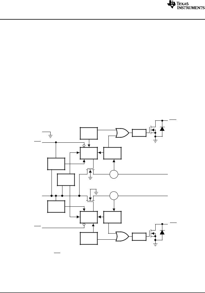
Figure 1. Functional Block Diagram (TPS2041B and TPS2051B) |
|
|
||||||||||||||||||||||||||||||||||||||||||||||||||
|
|
|
|
|
|
IN |
|
|
|
|
|
|
|
|
|
|
|
|
|
|
|
|
|
|
|
|
|
|
|
|
|
|
|
|
|
|
|
CS |
(See Note A) |
OUT |
||||||||||||||||||||||
|
|
|
|
|
|
|
|
|
|
|
|
|
|
|
|
|
|
|
|
|
|
|
|
|
|
|
|
|
|
|
|
|
|
|
|
|
||||||||||||||||||||||||||
|
|
|
|
|
|
|
|
|
|
|
|
|
|
|
|
|
|
|
|
|
|
|
|
|
|
|
|
|
|
|
|
|
|
|
|
|
||||||||||||||||||||||||||
|
|
|
|
|
|
|
|
|
|
|
|
|
|
|
|
|
|
|
|
|
|
|
|
|
|
|
|
|
|
|
|
|
|
|
|
|
|
|
|
|
|
|
|
|
|
|
|
|
|
|
|
|
|
|
|
|||||||
|
|
|
|
|
|
|
|
|
|
|
|
|
|
|
|
|
|
|
|
|
|
|
|
|
|
|
|
|
|
|
|
|
|
|
|
|
|
|
|
|
|
|||||||||||||||||||||
|
|
|
|
|
|
|
|
|
|
|
|
|
|
|
|
|
|
|
|
|
|
|
|
|
|
|
|
|
|
|
|
|
|
|
|
|
|
|
|
|
|
|
|
|
|
|
|
|
|
|
|
|
|
|
|
|
|
|
|
|||
|
|
|
|
|
|
|
|
|
|
|
|
|
|
|
|
|
|
|
|
|
|
|
|
|
|
|
|
|
|
|
|
|
|
|
|
|
|
|
|
|
|
|
|
|
|
|
|
|
|
|
|
|
|
|
|
|
|
|
|
|
|
|
|
|
|
|
|
|
|
|
|
|
|
|
|
|
|
|
|
|
|
|
|
|
|
|
|
|
|
|
|
|
|
|
|
|
|
|
|
|
|
|
|
|
|
|
|
|
|
|
|
|
|
|
|
|
|
|
|
|
|
|
|
|
|
|
|
|
|
|
|
|
|
|
|
|
|
Charge |
|
|
|
|
|
|
|
|
|
|
|
|
|
|
|
|
|
|
|
|
|
|
|
|
|
|
|
|
|
|
|
|
|
|
|
|
|
|
|
|
|
|
|
|
||||||
|
|
|
|
|
|
|
|
|
|
|
|
|
Pump |
|
|
|
|
|
|
|
|
|
|
|
|
|
|
|
|
|
|
|
|
|
|
|
|
|
|
|
|
|
|
|
|
|
|
|
|
|
|
|
|
|
|
|
|
|||||
|
|
|
|
|
|
|
|
|
|
|
|
|
|
|
|
|
|
|
|
|
|
|
|
|
|
|
|
|
|
|
|
|
|
|
|
|
|
|
|
|
|
|
|
|
|
|
|
|
|
|
|
|
|
|
|
|
||||||
|
|
|
|
|
|
|
|
|
|
|
|
|
|
|
|
|
|
|
|
|
|
|
|
|
|
|
|
|
|
|
|
|
|
|
|
|
|
|
|
|
|
|
|
|
|
|
|
|
|
|
|
|
|
|
|
|||||||
|
|
|
|
|
|
|
|
|
|
|
|
|
|
|
|
|
|
|
|
|
|
|
|
|
|
|
|
|
|
|
|
|
|
|
|
|
Current |
|
|
|
|
|
|
|
||||||||||||||||||
|
|
|
|
|
|
EN |
|
|
|
|
|
|
|
|
|
|
|
|
|
|
|
|
Driver |
|
|
|
|
|||||||||||||||||||||||||||||||||||
|
|
|
|
|
|
|
|
|
|
|
|
|
|
|
|
|
|
|
|
|
|
|
|
|
Limit |
|
|
|
|
|
|
|
|
|
|
|
|
|
|
|
|
|
|
|||||||||||||||||||
|
|
|
|
|
(See Note B) |
|
|
|
|
|
|
|
|
|
|
|
|
|
|
|
|
|
|
|
|
|
|
|
|
|
|
|
|
|
|
|
|
|
|
|
||||||||||||||||||||||
|
|
|
|
|
|
|
|
|
|
|
|
|
|
|
|
|
|
|
|
|
|
|
|
|
|
|
|
|
|
|
|
|
|
|
|
|
|
|
|
|
|
|
|
|
|
|
|
|
|
|
|
|
|
|
|
|
|
|||||
|
|
|
|
|
|
|
|
|
|
|
|
|
UVLO |
|
|
|
|
|
|
|
|
|
|
|
|
|
|
|
|
|
|
|
|
|
|
|
|
|
|
|
|
|
|
|
|
|
|
|
|
|
|
|
|
|
|
OC |
|
|||||
|
|
|
|
|
|
|
|
|
|
|
|
|
|
|
|
|
|
|
|
|
|
|
|
|
|
|
|
|
|
|
|
|
|
|
|
|
|
|
|
|
|
|
|
|
|
|
|
|
|
|
|
|
|
|
|
|
||||||
|
|
|
|
|
|
|
|
|
|
|
|
|
|
|
|
|
|
|
|
|
|
|
|
|
|
|
|
|
|
|
|
|
|
|
|
|
|
|
|
|
|
|
|
|
|
|
|
|
|
|
|
|
|
|
|
|
||||||
|
|
|
|
|
GND |
|
|
|
|
|
|
|
|
|
|
|
|
|
|
|
Thermal |
|
|
|
|
|
|
|
|
|
|
|
|
Deglitch |
|
|
|
|
|
|
|
|
|
|
|
|
|
|
|
|||||||||||||
|
|
|
|
|
|
|
|
|
|
|
|
|
|
|
|
|
|
|
|
|
|
|
|
|
|
|
|
|
|
|
|
|
|
|
|
|
|
|
|
|
|
|
|
|
|
|||||||||||||||||
|
|
|
|
|
|
|
|
|
|
|
|
|
|
|
|
|
|
|
|
|
Sense |
|
|
|
|
|
|
|
|
|
|
|
|
|
|
|
|
|
|
|
|
|
|
|
|
|
|
|
|
|||||||||||||
|
|
|
|
|
|
|
|
|
|
|
|
|
|
|
|
|
|
|
|
|
|
|
|
|
|
|
|
|
|
|
|
|
|
|
|
|
|
|
|
|
|
|
|
|
|
|
|
|||||||||||||||
|
|
|
|
|
|
|
|
|
|
|
|
|
|
|
|
|
|
|
|
|
|
|
|
|
|
|
|
|
|
|
|
|
|
|
|
|
|
|
|
|
|
|
|
|
|
|
|
|
|
|
|
|
|
|
|
|
|
|
|
|
|
|
|
|
|
|
|
|
|
|
|
|
|
|
|
|
|
|
|
|
|
|
|
|
|
|
|
|
|
|
|
|
|
|
|
|
|
|
|
|
|
|
|
|
|
|
|
|
|
|
|
|
|
|
|
|
|
|
|
|
|
|
|
|
|
Note A: Current sense
Note B: Active low (EN) for TPS2041B; Active high (EN) for TPS2051B
Copyright © 2010–2011, Texas Instruments Incorporated |
5 |
TPS2041B, TPS2042B
TPS2043B, TPS2044B, TPS2051B
TPS2052B, TPS2053B, TPS2054B
SLVS514L –JUNE 2010 –REVISED JUNE 2011 www.ti.com
Terminal Functions (TPS2042B and TPS2052B)
|
|
|
|
|
TERMINAL |
|
|
|
|
|
|
|
|
|
|
|
|
||
|
|
|
|
D, DGN, and DRB PACKAGES |
|
I/O |
DESCRIPTION |
||
|
|
|
|
|
|
|
|
|
|
|
NAME |
TPS2042B |
TPS2052B |
|
|
||||
|
|
|
|
|
|
|
|
||
|
|
|
3 |
|
- |
I |
Enable input, logic low turns on power switch IN-OUT1 |
||
|
EN1 |
|
|||||||
|
|
|
4 |
|
- |
I |
Enable input, logic low turns on power switch IN-OUT2 |
||
|
EN2 |
|
|||||||
|
EN1 |
- |
|
3 |
I |
Enable input, logic high turns on power switch IN-OUT1 |
|||
|
|
|
|
|
|
|
|
||
|
EN2 |
- |
|
4 |
I |
Enable input, logic high turns on power switch IN-OUT2 |
|||
|
|
|
|
|
|
|
|
||
|
GND |
1 |
|
1 |
|
Ground |
|||
|
|
|
|
|
|
|
|
||
|
IN |
2 |
|
2 |
I |
Input voltage |
|||
|
|
|
|
|
|
|
|
|
|
|
|
|
|
8 |
|
8 |
O |
Overcurrent, open-drain output, active low, IN-OUT1 |
|
|
OC1 |
|
|||||||
|
|
|
|
|
5 |
|
5 |
O |
Overcurrent, open-drain output, active low, IN-OUT2 |
|
OC2 |
|
|||||||
|
OUT1 |
7 |
|
7 |
O |
Power-switch output, IN-OUT1 |
|||
|
|
|
|
|
|
|
|
|
|
|
OUT2 |
6 |
|
6 |
O |
Power-switch output, IN-OUT2 |
|||
|
|
|
|
|
|
|
|
|
|
|
PowerPAD™ |
- |
|
- |
|
Internally connected to GND; used to heat-sink the part to the circuit board |
|||
|
|
|
traces. Should be connected to GND pin. |
||||||
|
|
|
|
|
|
|
|
|
|
|
|
|
|
|
|
|
|
|
|
Functional Block Diagram (TPS2042B and TPS2052B)
|
|
|
OC1 |
GND |
Thermal |
|
Deglitch |
Sense |
|
||
|
|
|
|
EN1 |
|
|
|
(See Note B) |
|
Current |
|
|
Driver |
|
|
|
Limit |
|
|
|
|
|
|
Charge |
|
|
|
Pump |
|
|
|
|
|
(See Note A) |
|
|
|
CS |
OUT1 |
UVLO |
|
|
|
|
|
(See Note A) |
|
IN |
|
CS |
OUT2 |
Charge |
|
|
|
Pump |
|
|
|
|
Driver |
Current |
|
|
Limit |
|
|
|
|
|
|
EN2 |
|
|
OC2 |
|
|
|
|
(See Note B) |
|
|
|
|
Thermal |
|
Deglitch |
|
Sense |
|
|
Note A: Current sense |
|
|
|
Note B: Active low (ENx) for TPS2042B; Active high (ENx) for TPS2052B |
|
||
6 |
Copyright © 2010–2011, Texas Instruments Incorporated |

|
TPS2041B, TPS2042B |
|
TPS2043B, TPS2044B, TPS2051B |
|
TPS2052B, TPS2053B, TPS2054B |
www.ti.com |
SLVS514L –JUNE 2010–REVISED JUNE 2011 |
Terminal Functions (TPS2043B and TPS2053B)
|
|
|
|
|
TERMINAL |
|
I/O |
DESCRIPTION |
|
|
|
|
|
|
|
||
|
NAME |
TPS2043B |
TPS2053B |
|||||
|
|
|
||||||
|
|
|
|
|
|
|
||
|
|
|
3 |
-- |
I |
Enable input, logic low turns on power switch IN1-OUT1 |
||
|
EN1 |
|||||||
|
|
|
4 |
-- |
I |
Enable input, logic low turns on power switch IN1-OUT2 |
||
|
EN2 |
|||||||
|
|
|
7 |
-- |
I |
Enable input, logic low turns on power switch IN2-OUT3 |
||
|
EN3 |
|||||||
|
EN1 |
-- |
3 |
I |
Enable input, logic high turns on power switch IN1-OUT1 |
|||
|
|
|
|
|
|
|
||
|
EN2 |
-- |
4 |
I |
Enable input, logic high turns on power switch IN1-OUT2 |
|||
|
|
|
|
|
|
|
||
|
EN3 |
-- |
7 |
I |
Enable input, logic high turns on power switch IN2-OUT3 |
|||
|
|
|
|
|
|
|
||
|
GND |
1, 5 |
1, 5 |
|
Ground |
|||
|
|
|
|
|
|
|
||
|
IN1 |
2 |
2 |
I |
Input voltage for OUT1 and OUT2 |
|||
|
|
|
|
|
|
|
||
|
IN2 |
6 |
6 |
I |
Input voltage for OUT3 |
|||
|
|
|
|
|
|
|
||
|
NC |
8, 9, 10 |
8, 9, 10 |
|
No connection |
|||
|
|
|
|
|
|
|
|
|
|
|
|
|
16 |
16 |
O |
Overcurrent, open-drain output, active low, IN1-OUT1 |
|
|
OC1 |
|||||||
|
|
|
|
|
13 |
13 |
O |
Overcurrent, open-drain output, active low, IN1-OUT2 |
|
OC2 |
|||||||
|
|
|
|
|
12 |
12 |
O |
Overcurrent, open-drain output, active low, IN2-OUT3 |
|
OC3 |
|||||||
|
OUT1 |
15 |
15 |
O |
Power-switch output, IN1-OUT1 |
|||
|
|
|
|
|
|
|
|
|
|
OUT2 |
14 |
14 |
O |
Power-switch output, IN1-OUT2 |
|||
|
|
|
|
|
|
|
|
|
|
OUT3 |
11 |
11 |
O |
Power-switch output, IN2-OUT3 |
|||
|
|
|
|
|
|
|
|
|
Copyright © 2010–2011, Texas Instruments Incorporated |
7 |
TPS2041B, TPS2042B
TPS2043B, TPS2044B, TPS2051B
TPS2052B, TPS2053B, TPS2054B
SLVS514L –JUNE 2010 –REVISED JUNE 2011 |
www.ti.com |
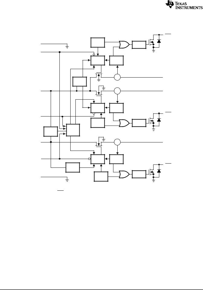
Figure 2. Functional Block Diagram (TPS2043B and TPS2053B)
|
|
|
OC1 |
GND |
Thermal |
|
|
Sense |
|
Deglitch |
|
EN1 |
|
|
|
(See Note B) |
|
Current |
|
|
Driver |
||
|
Limit |
|
|
|
|
|
|
|
|
CS |
(See Note A) |
|
|
OUT1 |
|
|
UVLO |
|
|
|
|
CS |
(See Note A) |
IN1 |
|
OUT2 |
|
|
Driver |
Current |
|
|
Limit |
|
|
|
|
|
|
EN2 |
|
|
OC2 |
|
|
|
|
(See Note B) |
Thermal |
|
Deglitch |
|
Sense |
|
|
|
|
|
|
VCC |
Charge |
|
|
Pump |
|
|
|
Selector |
|
|
|
|
|
|
|
|
|
|
(See Note A) |
IN2 |
|
CS |
OUT3 |
EN3 |
Driver |
Current |
|
Limit |
|
||
(See Note B) |
|
|
|
UVLO |
|
OC3 |
|
|
|
|
|
GND |
Thermal |
|
Deglitch |
Sense |
|
|
|
|
|
|
|
Note A: Current sense
Note B: Active low (ENx) for TPS2043B; Active high (ENx) for TPS2053B
8 |
Copyright © 2010–2011, Texas Instruments Incorporated |

|
TPS2041B, TPS2042B |
|
TPS2043B, TPS2044B, TPS2051B |
|
TPS2052B, TPS2053B, TPS2054B |
www.ti.com |
SLVS514L –JUNE 2010–REVISED JUNE 2011 |
Terminal Functions (TPS2044B and TPS2054B)
|
|
|
|
|
TERMINAL |
|
I/O |
DESCRIPTION |
|
|
|
|
|
|
|
||
|
NAME |
TPS2044B |
TPS2054B |
|||||
|
|
|
||||||
|
|
|
|
|
|
|
||
|
|
|
3 |
- |
I |
Enable input, logic low turns on power switch IN1-OUT1 |
||
|
EN1 |
|||||||
|
|
|
4 |
- |
I |
Enable input, logic low turns on power switch IN1-OUT2 |
||
|
EN2 |
|||||||
|
|
|
7 |
- |
I |
Enable input, logic low turns on power switch IN2-OUT3 |
||
|
EN3 |
|||||||
|
|
|
8 |
- |
I |
Enable input, logic low turns on power switch IN2-OUT4 |
||
|
EN4 |
|||||||
|
EN1 |
- |
3 |
I |
Enable input, logic high turns on power switch IN1-OUT1 |
|||
|
|
|
|
|
|
|
||
|
EN2 |
- |
4 |
I |
Enable input, logic high turns on power switch IN1-OUT2 |
|||
|
|
|
|
|
|
|
||
|
EN3 |
- |
7 |
I |
Enable input, logic high turns on power switch IN2-OUT3 |
|||
|
|
|
|
|
|
|
||
|
EN4 |
- |
8 |
I |
Enable input, logic high turns on power switch IN2-OUT4 |
|||
|
|
|
|
|
|
|
||
|
GND |
1, 5 |
1, 5 |
|
Ground |
|||
|
|
|
|
|
|
|
||
|
IN1 |
2 |
2 |
I |
Input voltage for OUT1 and OUT2 |
|||
|
|
|
|
|
|
|
||
|
IN2 |
6 |
6 |
I |
Input voltage for OUT3 and OUT4 |
|||
|
|
|
|
|
|
|
|
|
|
|
|
|
16 |
16 |
O |
Overcurrent, open-drain output, active low, IN1-OUT1 |
|
|
OC1 |
|||||||
|
|
|
|
|
13 |
13 |
O |
Overcurrent, open-drain output, active low, IN1-OUT2 |
|
OC2 |
|||||||
|
|
|
|
|
12 |
12 |
O |
Overcurrent, open-drain output, active low, IN2-OUT3 |
|
OC3 |
|||||||
|
|
|
|
|
9 |
9 |
O |
Overcurrent, open-drain output, active low, IN2-OUT4 |
|
OC4 |
|||||||
|
OUT1 |
15 |
15 |
O |
Power-switch output, IN1-OUT1 |
|||
|
|
|
|
|
|
|
|
|
|
OUT2 |
14 |
14 |
O |
Power-switch output, IN1-OUT2 |
|||
|
|
|
|
|
|
|
|
|
|
OUT3 |
11 |
11 |
O |
Power-switch output, IN2-OUT3 |
|||
|
|
|
|
|
|
|
|
|
|
OUT4 |
10 |
10 |
O |
Power-switch output, IN2-OUT4 |
|||
|
|
|
|
|
|
|
|
|
Copyright © 2010–2011, Texas Instruments Incorporated |
9 |
TPS2041B, TPS2042B
TPS2043B, TPS2044B, TPS2051B
TPS2052B, TPS2053B, TPS2054B
SLVS514L –JUNE 2010 –REVISED JUNE 2011 |
www.ti.com |
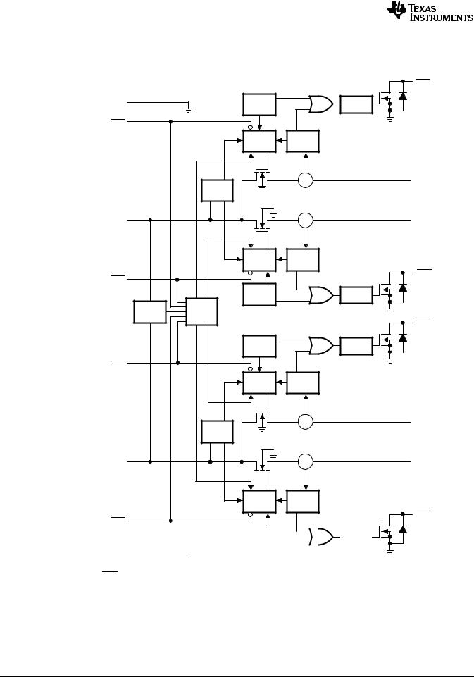
Figure 3. Functional Block Diagram (TPS2044B and TPS2054B)
|
|
|
OC1 |
GND |
Thermal |
|
Deglitch |
Sense |
|
||
|
|
||
|
|
|
|
EN1 |
|
|
|
(See Note B) |
Driver |
Current |
|
|
|
||
|
Limit |
|
|
|
|
|
|
|
|
|
(See Note A) |
|
|
CS |
OUT1 |
|
UVLO |
|
|
|
Power Switch |
|
|
|
|
|
(See Note A) |
IN1 |
|
CS |
OUT2 |
|
Driver |
Current |
|
|
Limit |
|
|
|
|
|
|
EN2 |
|
|
OC2 |
|
|
|
|
(See Note B) |
Thermal |
|
Deglitch |
|
Sense |
|
|
|
|
|
|
VCC |
Charge |
|
|
Selector |
Pump |
|
|
|
|
|
OC3 |
|
Thermal |
|
Deglitch |
|
Sense |
|
|
|
|
|
|
EN3 |
|
|
|
(See Note B) |
Driver |
Current |
|
|
|
||
|
Limit |
|
|
|
|
|
|
|
|
|
(See Note A) |
|
|
CS |
OUT3 |
|
UVLO |
|
|
|
Power Switch |
|
|
|
|
|
(See Note A) |
IN2 |
|
CS |
OUT4 |
|
Driver |
Current |
|
|
Limit |
|
|
|
|
|
|
EN4 |
|
|
OC4 |
|
|
|
|
(See Note B) |
Thermal |
|
|
|
|
|
|
|
|||||||
|
|
|
|
|
Deglitch |
|
|||||||||
|
|
|
|
|
|
||||||||||
|
|
|
|
|
|
|
|
|
|
|
|
|
|||
GND |
|
|
|
|
|
|
Sense |
|
|
|
|
|
|
|
|
|
|
|
|
|
|
|
|
|
|
|
|
|
|
||
|
|
|
|
|
|
|
|
|
|
|
|
|
|
|
|
|
|
|
|
|
|
|
|
|
|
|
|
|
|
|
|
|
|
|
|
|
|
|
|
|
|
|
|
|
|
|
|
|
|
|
|
|
|
|
|
|
|
|
|
|
|
|
|
Note A: Current sense
Note B: Active low (ENx) for TPS2044B; Active high (ENx) for TPS2054B
10 |
Copyright © 2010–2011, Texas Instruments Incorporated |
|
|
|
|
|
|
|
|
|
|
|
|
|
|
|
|
|
|
|
|
|
|
|
|
|
|
|
|
|
|
|
|
|
|
|
|
|
|
|
|
|
|
|
|
|
|
|
|
|
|
|
|
|
|
|
|
|
|
|
|
|
|
|
|
TPS2041B, TPS2042B |
||||||||||||||||||||||
|
|
|
|
|
|
|
|
|
|
|
|
|
|
|
|
|
|
|
|
|
|
|
|
|
|
|
|
|
|
|
|
|
|
|
|
|
|
|
|
|
|
|
|
|
|
|
|
TPS2043B, TPS2044B, TPS2051B |
||||||||||||||||||||||||||||||||||||||
|
|
|
|
|
|
|
|
|
|
|
|
|
|
|
|
|
|
|
|
|
|
|
|
|
|
|
|
|
|
|
|
|
|
|
|
|
|
|
|
|
|
|
|
|
|
|
|
TPS2052B, TPS2053B, TPS2054B |
||||||||||||||||||||||||||||||||||||||
www.ti.com |
|
|
|
|
|
|
|
|
|
|
|
|
|
|
|
|
|
|
|
|
|
|
|
|
|
|
|
|
|
|
|
|
|
|
|
|
|
|
|
|
|
|
|
|
|
|
|
|
SLVS514L –JUNE 2010–REVISED JUNE 2011 |
|||||||||||||||||||||||||||||||||||||
|
|
|
|
|
|
|
|
|
|
|
|
|
|
|
|
PARAMETER MEASUREMENT INFORMATION |
|
|
|
|
|
|
|
|
|
|
|
|
|
|
|
|
|
|
|
|
|
|
|
|||||||||||||||||||||||||||||||||||||||||||||||
|
|
|
|
|
|
|
|
OUT |
|
|
|
|
|
|
|
|
|
|
|
|
|
|
|
|
|
|
|
|
|
|
|
|
|
|
|
|
|
|
|
tr |
|
|
|
|
|
|
|
|
|
|
|
|
|
|
|
|
|
|
|
|
|
|
|
|
|
|
|
|
|
|
|
|
|
|
|
tf |
||||||||||
|
|
|
|
|
|
|
|
|
|
|
|
|
|
|
RL |
|
|
|
|
|
|
|
CL |
|
|
|
|
|
|
|
|
|
|
|
|
|
|
|
|
|
|
|
|
|
|
|
|
|
|
|
|
|
|
|
|
|
|
|
|
|
|
|
|
|
||||||||||||||||||||||
|
|
|
|
|
|
|
|
|
|
|
|
|
|
|
|
|
|
|
|
|
|
|
|
|
|
|
|
|
|
|
|
|
|
|
|
|
|
|
|
|
|
|
|
|
|
|
|
|
|
|
|
|
|
|
|
|
|
|
|
|
|
|
|
|
|
|
|
|
|
|
||||||||||||||||
|
|
|
|
|
|
|
|
|
|
|
|
|
|
|
|
|
|
|
|
|
|
|
|
|
|
|
|
|
|
|
|
|
|
|
|
|
|
|
|
|
|
|
|
|
|
|
|
|
|
|
|
|
|
|
|
|
|
|
|
|
|
|
|
|
|
|
|
|
||||||||||||||||||
|
|
|
|
|
|
|
|
|
|
|
|
|
|
|
|
|
|
|
|
|
|
|
|
|
|
|
|
|
|
|
|
|
VO(OUT) |
|
|
|
|
|
|
|
|
|
|
|
|
|
|
|
|
|
|
|
|
|
|
|
|
|
|
|
|
|
|
|
|
|
|
|
|
|
|
|
||||||||||||||
|
|
|
|
|
|
|
|
|
|
|
|
|
|
|
|
|
|
|
|
|
|
|
|
|
|
|
|
|
|
|
|
|
|
|
|
|
|
|
|
|
|
|
|
|
|
|
|
|
|
|
|
|
|
|
|
|
|
|
|
|
|
|
|
|
|
|
|
|
|
|
|
|
|
|
|
|
|
|
|
|||||||
|
|
|
|
|
|
|
|
|
|
|
|
|
|
|
|
|
|
|
|
|
|
|
|
|
|
|
|
|
|
|
|
|
|
|
|
|
|
|
|
|
|
|
|
|
|
|
|
|
|
|
|
90% 90% |
|
|
|
|
|
|
|
|
|
|
|
|
|
|
|
|
|
|||||||||||||||||
|
|
|
|
|
|
|
|
|
|
|
|
|
|
|
|
|
|
|
|
|
|
|
|
|
|
|
|
|
|
|
|
|
|
|
|
|
|
|
|
|
|
|
|
|
|
|
|
|
|
|
|
|
|
|
|
|
|
|
|
|
|
|
|
|
|
|
|
|
||||||||||||||||||
|
|
|
|
|
|
|
|
|
|
|
|
|
|
|
|
|
|
|
|
|
|
|
|
|
|
|
|
|
|
|
|
|
|
|
|
|
|
|
|
|
|
|
|
|
|
|
|
|
|
|
|
|
|
|
10% |
10% |
|
|
|
|
|
|
|
|
|
|
|
|
||||||||||||||||||
|
|
|
|
|
|
|
|
|
|
|
|
|
TEST CIRCUIT |
|
|
|
|
|
|
|
|
|
|
|
|
|
|
|
|
|
|
|
|
|
|
|
|
|
|
|
|
|
|
|
|
|
|
|
|
|
|
|
|
|
|
|
|
|
|
|
|
|
|
|
|
|
|
|
|
|
|
|||||||||||||||
|
|
|
|
|
|
|
|
|
|
|
|
|
|
50% |
|
|
|
|
|
|
|
|
|
|
|
|
|
|
|
|
|
|
|
|
|
|
|
|
|
|
|
|
|
|
|
|
|
|
|
|
|
|
|
|
|
|
|
|
|
|
|
|
|
|
|
|
|
|
|
|
|
|
|
|
|
|
|
|||||||||
|
|
|
V |
|
|
|
|
|
|
|
|
50% |
|
|
|
|
|
|
|
|
|
|
|
|
|
|
|
|
|
|
VI(EN) |
|
|
50% |
|
|
|
|
|
|
50% |
|
|
|
|
|
|
|
|
|
|
|
|
|
|
|
|
|
|
|
|
|
|
|||||||||||||||||||||||
I(EN) |
|
|
|
|
|
|
|
|
|
|
|
|
|
|
|
|
|
|
|
|
|
|
|
|
|
|
|
|
|
|
|
|
|
|
|
|
|
|
|
|
|
|
|
|
|
|
|
|
|
|
|
|
|
|
|
|
|
|
|
|
|
|||||||||||||||||||||||||
|
|
|
|
|
|
|
|
|
|
|
|
|
|
|
|
|
|
|
|
|
|
|
|
|
|
|
|
|
|
|
|
|
|
|
|
|
|
|
|
|
|
|
|
|
|
|
|
|
|
|
|
|
|
|
|
|
|
|
|
|
|
|
|
|
|
|
|
|
|
|
|
|
|
|
|
|
|
|
|
|
|
|||||
|
|
|
|
|
|
ton |
|
|
|
|
|
|
|
|
|
|
|
|
|
|
|
|
|
|
|
|
|
|
|
toff |
|
|
|
|
|
ton |
|
|
|
|
|
|
|
|
|
|
|
|
|
|
|
|
|
|
|
|
|
|
|
|
|
|
|
|
|
|
|
|
|
|
|
|
toff |
|||||||||||||
|
|
|
|
|
|
|
|
|
|
|
|
|
|
|
|
|
|
|
|
|
|
|
|
|
|
|
|
|
|
|
|
|
|
|
|
|
|
|
|
|
|
|
|
|
|
|
|
|
|
|
|
|
|
|
|
|
|
|
|
|
|
|||||||||||||||||||||||||
|
|
|
|
|
|
|
|
|
|
|
|
|
|
|
|
|
|
|
|
|
|
|
|
|
|
|
|
|
|
|
|
|
|
|
|
|
|
|
|
|
|
|
|
|
|
|
|
|
|
|
|
|
|
|
|
|
|
|
|
|
|
|
|
|
|
|
|
|
|
|
|
|
|
|
|
|
|
|
|
|
|
|
|
|||
|
|
VO(OUT) |
|
|
|
|
|
|
|
|
|
|
|
|
|
|
90% |
|
|
|
|
|
10% |
|
|
|
|
|
|
VO(OUT) |
|
|
|
|
|
|
|
|
|
|
|
|
|
|
|
|
90% |
|
|
|
|
|
|
|
|
|
|
|
|
|
|
|
|
|
|
|
|
|
|
|||||||||||||||||
|
|
|
|
|
|
|
|
|
|
|
|
|
|
|
|
|
|
|
|
|
|
|
|
|
|
|
|
|
|
|
|
|
|
|
|
|
|
|
|
|
|
|
|
|
|
|
|
|
|
|
|
|
|
|
|
|
|
10% |
|
|
|
|
|
|
|
|
|
|
||||||||||||||||||
|
|
|
|
|
|
|
|
|
|
|
|
|
|
|
|
|
|
|
|
|
|
|
|
|
|
|
|
|
|
|
|
|
|
|
|
|
|
|
|
|
|
|
|
|
|
|
|
|
|
|
|
|
|
|
|
|
|
|
|
|
||||||||||||||||||||||||||
|
|
|
|
|
|
|
|
|
|
|
|
|
|
|
|
|
|
|
|
|
|
|
|
|
|
|
|
|
|
|
|
|
|
|
|
|
|
VOLTAGE WAVEFORMS |
|
|
|
|
|
|
|
|
|
|
|
|
|
|
|
|
|
|
|
|
|
|
|
|
|
|
|
|
|
|
|
|
|
|
|
|
|
|
|
|||||||||
|
|
|
|
|
|
|
|
|
|
|
|
|
|
|
|
|
|
|
|
|
Figure 4. Test Circuit and Voltage Waveforms |
|
|
|
|
|
|
|
|
|
|
|
|
|
|
|
|
|
|
|
|
|
|
|
||||||||||||||||||||||||||||||||||||||||||
|
|
|
|
|
|
|
|
|
|
|
|
|
|
|
|
|
|
|
|
|
|
|
|
|
|
|
|
|
|
|
|
|
|
|
|
|
|
|
|
|
|
|
|
|
|
|
|
|
|
|
|
|
|
|
|
|
|
|
|
|
|
|
|
|
|
|
|
|
|
|
|
|
|
|||||||||||||
|
|
|
|
|
|
|
|
|
|
|
|
|
|
|
|
|
|
|
|
|
|
|
|
|
|
|
|
|
RL = 10 W, |
|
|
|
|
|
|
|
|
|
|
|
|
|
|
|
|
|
|
|
|
|
|
|
|
|
|
|
|
|
|
|
|
|
|
|
|
|
|
|
|
|
|
|
|
|||||||||||||
VI(EN) |
|
|
|
|
|
|
|
|
|
|
|
|
|
|
|
|
|
|
|
|
|
|
|
|
|
|
|
|
V |
|
|
|
|
|
|
|
|
|
|
|
|
|
|
|
|
|
|
|
|
|
|
|
|
|
|
|
|
|
|
|
|
|
|
|
|
|
|
|
|
|
|
|||||||||||||||
|
|
|
|
|
|
|
|
|
|
|
|
|
|
|
|
|
|
|
|
|
|
|
|
|
|
|
|
|
|
|
|
|
|
|
|
|
|
|
|
|
|
|
|
|
|
|
|
|
|
|
|
|
|
|
|
|
|
|
|
|
|
|
|
|
||||||||||||||||||||||
VI(EN) |
|
|
|
|
|
|
|
|
|
|
|
|
|
|
|
|
|
|
|
|
|
|
|
|
|
CL = 1 mF |
|
I(EN) |
|
|
|
|
|
|
|
|
|
|
|
|
|
|
|
|
|
|
|
|
|
|
|
|
|
|
|
|
|
|
|
|
|
|
|
|
|
|
|
|||||||||||||||||||
|
|
|
|
|
|
|
|
|
|
|
|
|
|
|
|
|
|
|
|
|
|
|
|
|
|
V |
|
|
|
|
|
|
|
|
|
|
|
|
|
|
|
|
|
|
|
|
|
|
|
|
|
|
|
|
|
|
|
|
|
|
|
|
|
|
|
|||||||||||||||||||||
5 V/div |
|
|
|
|
|
|
|
|
|
|
|
|
|
|
|
|
|
|
|
|
|
|
|
|
|
TA = 255C |
|
I(EN) |
|
|
|
|
|
|
|
|
|
|
|
|
|
|
|
|
|
|
|
|
|
|
|
|
|
|
|
|
|
|
|
|
|
|
|
|
|
|
|
|||||||||||||||||||
|
|
|
|
|
|
|
|
|
|
|
|
|
|
|
|
|
|
|
|
|
|
|
|
|
|
5 V/div |
|
|
|
|
|
|
|
|
|
|
|
|
|
|
|
|
|
|
|
|
|
|
|
|
|
|
|
|
|
|
|
|
|
|
|
|
|
|
|
|||||||||||||||||||||
|
|
|
|
|
|
|
|
|
|
|
|
|
|
|
|
|
|
|
|
|
|
|
|
|
|
|
|
|
|
|
|
|
|
|
|
|
|
|
|
|
|
|
|
|
|
|
|
|
|
|
|
|
|
|
|
|
|
|
|
|
|
|
|
|
|
|
|
|
|
|
|
|
||||||||||||||
|
|
|
VO(OUT) |
RL = 10 W, |
|
|
|
|
2 V/div |
CL = 1 mF |
|
V |
|
TA = 255C |
|||
O(OUT) |
|
|
|
||
2 V/div |
|
|
|
||
|
|
|
|
|
|
|
|
|
|
t − T ime − 500 ms/div |
|
|
t − T ime − 500 ms/div |
|
|||
|
|
|
|
||
Figure 5. Turnon Delay and Rise Time With 1-μF |
Figure 6. Turnoff Delay and Fall Time With 1-μF |
||||
|
Load |
|
Load |
||
Copyright © 2010–2011, Texas Instruments Incorporated |
11 |
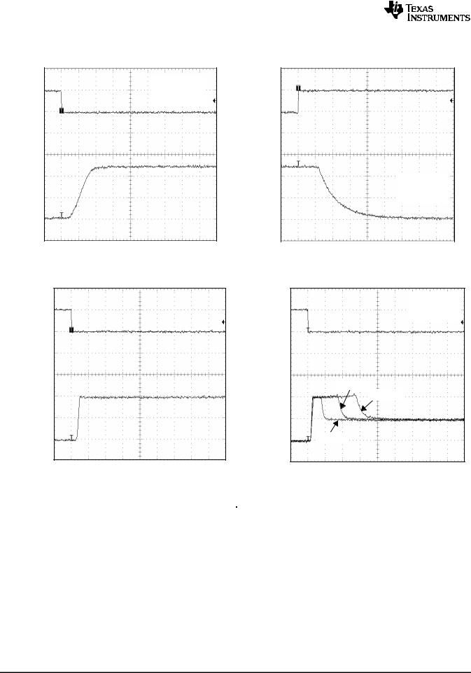
TPS2041B, TPS2042B
TPS2043B, TPS2044B, TPS2051B
TPS2052B, TPS2053B, TPS2054B
SLVS514L –JUNE 2010 –REVISED JUNE 2011 |
|
|
|
|
www.ti.com |
||||
|
|
|
PARAMETER MEASUREMENT INFORMATION (continued) |
||||||
|
|
|
|
|
|
|
|
|
|
|
|
|
RL = 10 W, |
|
|
|
|
|
|
|
|
|
VI(EN) |
||||||
VI(EN) |
|
C |
= 100 mF |
||||||
VI(EN) |
L |
|
VI(EN) |
||||||
T |
= 255C |
||||||||
5 V/div |
A |
|
5 V/div |
||||||
|
|
|
|
|
|
|
|||
|
|
VO(OUT) |
RL = 10 W, |
|
|
|
CL = 100 mF |
||
|
|
2 V/div |
TA = 255C |
|
VO(OUT) |
|
|
||
2 V/div |
|
|
||
|
|
|
|
|
|
t − T ime − 500 ms/div |
t − T ime − 500 ms/div |
||
Figure 7. Turnon Delay and Rise Time With 100-μF Figure 8. Turnoff Delay and Fall Time With 100-μF |
||||
|
Load |
Load |
||
|
|
|
|
|
|
V |
|
|
VI(EN) |
||
I(EN) |
VI(EN) |
||||
V |
|||||
I(EN) |
5 V/div |
||||
5 V/div |
|||||
IO(OUT) |
IO(OUT) |
500 mA/div |
|
500 mA/div |
|
t − T ime − 500 ms/div
VI = 5 V, |
RL = 10 W, |
TA = 255C |
220 mF |
470 mF |
100 mF |
t − T ime − 500 ms/div |
Figure 9. Short-Circuit Current, |
Figure 10. Inrush Current With Different |
Device Enabled Into Short |
Load Capacitance |
12 |
Copyright © 2010–2011, Texas Instruments Incorporated |
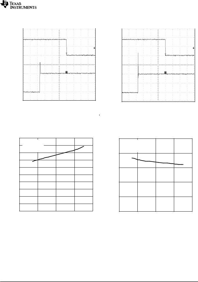
|
TPS2041B, TPS2042B |
|
TPS2043B, TPS2044B, TPS2051B |
|
TPS2052B, TPS2053B, TPS2054B |
www.ti.com |
SLVS514L –JUNE 2010–REVISED JUNE 2011 |
|
|
|
PARAMETER MEASUREMENT INFORMATION (continued) |
||||
|
|
|
|
|
|
|
|
VO(OC) |
|
|
V |
|
|
|
|
|
|
|
|||||
2 V/div |
|
O(OC) |
|||||
|
2 V/div |
||||||
IO(OUT) |
IO(OUT) |
500 mA/div |
500 mA/div |
t − T ime − 2 ms/div |
t − T ime − 2 ms/div |
|
Figure 11. 3-Ω Load Connected to Enabled Device Figure 12. 2-Ω Load Connected to Enabled Device
TYPICAL CHARACTERISTICS
TURNON TIME vs
INPUT VOLTAGE
|
1.0 |
|
|
|
|
|
0.9 |
CL = 100 mF, |
|
|
|
|
RL = 10 W, |
|
|
|
|
|
0.8 |
TA = 255C |
|
|
|
|
|
|
|
|
|
|
0.7 |
|
|
|
|
− ms |
0.6 |
|
|
|
|
Time |
0.5 |
|
|
|
|
Turnon |
0.4 |
|
|
|
|
0.3 |
|
|
|
|
|
|
|
|
|
|
|
|
0.2 |
|
|
|
|
|
0.1 |
|
|
|
|
|
0 |
|
|
|
|
|
2 |
3 |
4 |
5 |
6 |
|
|
|
VI − Input V oltage − V |
|
|
Figure 13.
TURNOFF TIME vs
INPUT VOLTAGE
|
3.3 |
CL = 100 mF, |
|
|
|
|
|
|
|
|
|
|
|
RL = 10 W, |
|
|
|
|
3.2 |
TA = 255C |
|
|
|
|
|
|
|
|
|
− ms |
3.1 |
|
|
|
|
Time |
|
|
|
|
|
|
|
|
|
|
|
Turnoff |
3 |
|
|
|
|
|
|
|
|
|
|
|
2.9 |
|
|
|
|
|
2.8 |
3 |
4 |
5 |
6 |
|
2 |
||||
|
|
VI |
− Input V oltage − V |
|
|
Figure 14.
Copyright © 2010–2011, Texas Instruments Incorporated |
13 |
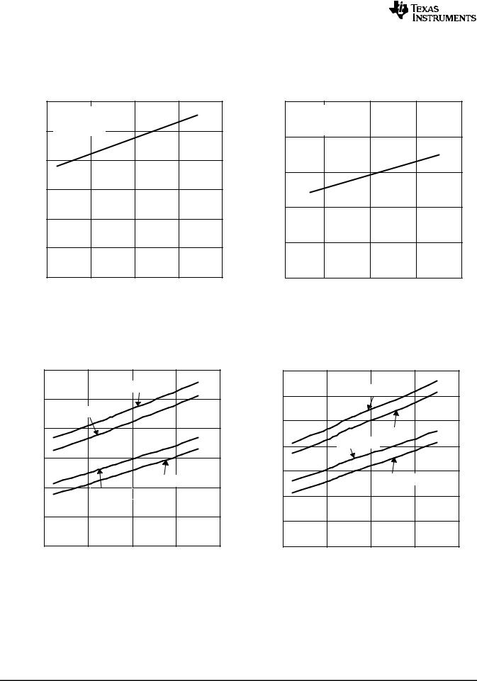
TPS2041B, TPS2042B
TPS2043B, TPS2044B, TPS2051B
TPS2052B, TPS2053B, TPS2054B
SLVS514L –JUNE 2010 –REVISED JUNE 2011 |
www.ti.com |
TYPICAL CHARACTERISTICS (continued)
RISE TIME vs
INPUT VOLTAGE
|
0.6 |
CL = 1 mF, |
|
|
|
|
|
|
|
|
|
|
|
RL = 10 W, |
|
|
|
|
0.5 |
TA = 255C |
|
|
|
− ms |
0.4 |
|
|
|
|
|
|
|
|
|
|
Rise Time |
0.3 |
|
|
|
|
0.2 |
|
|
|
|
|
|
|
|
|
|
|
|
0.1 |
|
|
|
|
|
0 |
|
|
|
|
|
2 |
3 |
4 |
5 |
6 |
|
|
|
VI − Input V oltage − V |
|
|
Figure 15.
FALL TIME vs
INPUT VOLTAGE
|
0.25 |
CL = 1 mF, |
|
|
|
|
|
|
|
|
|
|
|
RL = 10 W, |
|
|
|
|
0.2 |
TA = 255C |
|
|
|
|
|
|
|
|
|
ms |
0.15 |
|
|
|
|
Fall Time − |
|
|
|
|
|
0.1 |
|
|
|
|
|
|
0.05 |
|
|
|
|
|
0 |
|
|
|
|
|
2 |
3 |
4 |
5 |
6 |
|
|
|
VI − Input V oltage − V |
|
|
Figure 16.
TPS2041B/2051B |
TPS2042B/TPS2052B |
SUPPLY CURRENT, OUTPUT ENABLED |
SUPPLY CURRENT, OUTPUT ENABLED |
vs |
vs |
JUNCTION TEMPERATURE |
JUNCTION TEMPERATURE |
μ A |
60 |
|
|
|
|
70 |
|
|
VI = 5.5 V |
|
μ A |
|
|
− |
50 |
|
|
|
− |
60 |
Enabled |
|
|
|
Enabled |
||
|
|
|
|
|||
|
VI = 5 V |
|
|
|
||
40 |
|
|
|
50 |
||
|
|
|
|
|||
Output |
|
|
|
Output |
|
|
|
|
|
|
40 |
||
30 |
|
|
|
|
||
Current, |
|
|
|
Current, |
|
|
|
|
|
|
30 |
||
20 |
|
|
VI = 2.7 V |
|
||
− Supply |
|
VI = 3.3 V |
|
− Supply |
|
|
|
|
|
20 |
|||
10 |
|
|
|
|
||
I (IN) |
|
|
|
(IN) |
10 |
|
|
|
|
|
|||
|
|
|
|
|
||
I |
|
|
|
|
I |
|
|
|
|
|
|
I |
|
|
0 |
0 |
50 |
100 |
150 |
0 |
|
−50 |
|
||||
|
|
TJ − Junction T emperature − 5C |
|
|
||
|
|
VI = 5.5 V |
|
|
|
|
VI = 3.3 V |
VI = 5 V |
|
|
|
|
|
|
|
|
|
VI = 2.7 V |
|
−50 |
0 |
50 |
100 |
150 |
|
TJ − Junction T emperature − 5C |
|
||
Figure 17. |
Figure 18. |
14 |
Copyright © 2010–2011, Texas Instruments Incorporated |
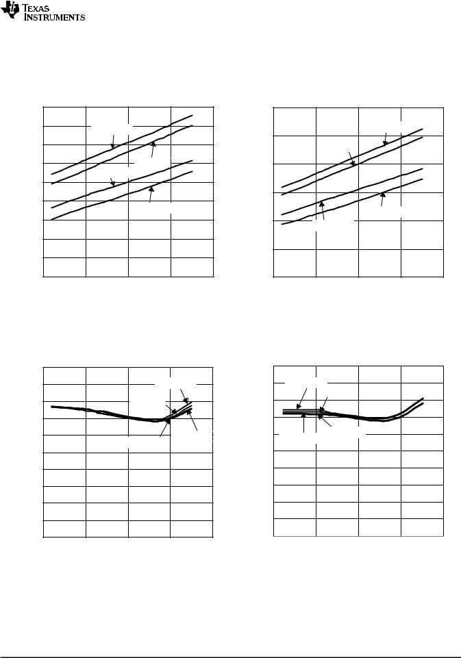
|
TPS2041B, TPS2042B |
|
TPS2043B, TPS2044B, TPS2051B |
|
TPS2052B, TPS2053B, TPS2054B |
www.ti.com |
SLVS514L –JUNE 2010–REVISED JUNE 2011 |
TYPICAL CHARACTERISTICS (continued) |
|
TPS2043B/TPS2053B |
TPS2044B/2054B |
SUPPLY CURRENT, OUTPUT ENABLED |
SUPPLY CURRENT, OUTPUT ENABLED |
vs |
vs |
JUNCTION TEMPERATURE |
JUNCTION TEMPERATURE |
|
90 |
|
|
|
μ A |
120 |
μ A |
80 |
|
VI = 5.5 V |
|
|
|
− |
|
|
− |
100 |
||
Enabled |
|
|
|
|
Enabled |
|
70 |
|
|
|
|
||
60 |
|
|
VI = 5 V |
80 |
||
Output |
|
VI = 3.3 V |
Output |
|||
|
|
|
|
|||
50 |
|
|
|
|
||
Current, |
40 |
|
|
|
Current, |
60 |
|
|
VI = 2.7 V |
|
|||
|
|
|
|
|||
|
|
|
|
|
||
Supply |
30 |
|
|
|
Supply |
40 |
20 |
|
|
|
|
||
− |
|
|
|
− |
|
|
|
|
|
|
|
||
I (IN) |
10 |
|
|
|
(IN) |
20 |
|
|
|
|
|||
I |
|
|
|
|
I |
|
|
|
|
|
|
I |
|
|
0 |
|
|
|
|
0 |
|
−50 |
0 |
50 |
100 |
150 |
|
|
|
TJ − Junction T emperature − 5C |
|
|
||
|
|
|
VI = 5.5 V |
|
|
VI = 5 V |
|
|
|
|
|
|
VI = 2.7 V |
|
|
VI = 3.3 V |
|
|
|
−50 |
0 |
50 |
100 |
150 |
|
TJ − Junction T emperature − 5C |
|
||
Figure 19. |
Figure 20. |
TPS2041B/2051B
SUPPLY CURRENT, OUTPUT DISABLED vs
JUNCTION TEMPERATURE
|
0.5 |
|
|
|
|
μ A |
0.45 |
|
|
VI = 5.5 V |
|
− |
|
|
|
|
|
Disabled |
0.4 |
|
|
VI = 5 V |
|
0.35 |
|
|
|
|
|
|
|
|
|
|
|
Output |
0.3 |
|
|
VI = 3.3 V |
|
|
|
|
VI = 2.7 V |
|
|
0.25 |
|
|
|
|
|
Current, |
|
|
|
|
|
0.2 |
|
|
|
|
|
|
|
|
|
|
|
Supply |
0.15 |
|
|
|
|
0.1 |
|
|
|
|
|
− |
|
|
|
|
|
|
|
|
|
|
|
(IN) |
0.05 |
|
|
|
|
I |
|
|
|
|
|
|
|
|
|
|
|
I |
|
|
|
|
|
|
0 |
0 |
50 |
100 |
150 |
|
−50 |
||||
|
|
TJ − Junction T emperature − 5C |
|
||
Figure 21.
TPS2042B/TPS2052B
SUPPLY CURRENT, OUTPUT DISABLED vs
JUNCTION TEMPERATURE
μ A |
0.5 |
|
|
|
|
0.45 |
VI = 5.5 V |
|
|
|
|
|
VI = 5 V |
|
|
||
− |
|
|
|
|
|
Disabled |
0.4 |
|
|
|
|
|
|
|
|
||
0.35 |
|
|
|
|
|
|
|
|
|
|
|
Output |
0.3 |
VI = 2.7 V |
VI = 3.3 V |
|
|
|
|
|
|
||
0.25 |
|
|
|
|
|
Current, |
|
|
|
|
|
0.2 |
|
|
|
|
|
|
|
|
|
|
|
− Supply |
0.15 |
|
|
|
|
0.1 |
|
|
|
|
|
(IN) |
0.05 |
|
|
|
|
I |
|
|
|
|
|
|
|
|
|
|
|
I |
|
|
|
|
|
|
0 |
0 |
50 |
100 |
150 |
|
−50 |
||||
|
|
TJ − Junction T emperature − 5C |
|
||
Figure 22.
Copyright © 2010–2011, Texas Instruments Incorporated |
15 |

TPS2041B, TPS2042B
TPS2043B, TPS2044B, TPS2051B
TPS2052B, TPS2053B, TPS2054B
SLVS514L –JUNE 2010 –REVISED JUNE 2011 www.ti.com
TYPICAL CHARACTERISTICS (continued)
TPS2043B/TPS2053B |
TPS2044B/2054B |
SUPPLY CURRENT, OUTPUT DISABLED |
SUPPLY CURRENT, OUTPUT DISABLED |
vs |
vs |
JUNCTION TEMPERATURE |
JUNCTION TEMPERATURE |
μ A |
0.5 |
|
|
|
|
μ A |
0.5 |
|
|
|
|
0.45 |
|
|
VI = 5.5 V |
|
0.45 |
VI = 5.5 V |
|
|
|||
DisabledOutputCurrent,Supply− − |
VI = 5 V |
|
|
|
DisabledOutputCurrent,Supply− − |
|
|
||||
|
|
|
|
|
|
VI = 5 V |
|
|
|||
0.1 |
|
|
|
|
0.1 |
|
|
|
|||
|
0.4 |
|
|
|
|
|
0.4 |
|
|
|
|
|
0.35 |
|
|
|
|
|
0.35 |
|
|
|
|
|
0.3 |
VI = 3.3 V |
|
|
|
|
0.3 |
VI = 2.7 V |
VI = 3.3 V |
|
|
|
|
VI = 2.7 V |
|
|
|
|
|
||||
|
|
|
|
|
|
|
|
|
|
||
|
0.25 |
|
|
|
|
|
|
|
|
|
|
|
|
|
|
|
|
0.25 |
|
|
|
|
|
|
0.2 |
|
|
|
|
|
0.2 |
|
|
|
|
|
0.15 |
|
|
|
|
|
0.15 |
|
|
|
|
(IN) |
0.05 |
|
|
|
|
(IN) |
0.05 |
|
|
|
|
I |
|
|
|
|
|
I |
|
|
|
|
|
I |
|
|
|
|
|
I |
|
|
|
|
|
|
0 |
|
|
|
|
|
0 |
|
|
|
|
|
−50 |
0 |
50 |
100 |
150 |
|
−50 |
0 |
50 |
100 |
150 |
|
|
TJ − Junction T emperature − 5C |
|
|
|
TJ − Junction T emperature − 5C |
|
||||
Figure 23.
STATIC DRAIN-SOURCE ON-STATE RESISTANCE vs
JUNCTION TEMPERATURE
Ω |
120 |
|
|
|
|
m |
|
|
|
|
|
IO = 0.5 A |
|
|
|
||
|
|
|
|
||
− |
|
|
VI = 2.7 V |
|
|
Resistance |
100 |
|
|
|
|
|
|
|
|
||
80 |
|
|
|
|
|
On-State |
|
|
VI |
= 3.3 V |
|
60 |
|
|
|
|
|
|
|
|
|
|
|
Drain-Source |
VI |
= 5 V |
|
|
|
40 |
|
|
|
|
|
|
|
|
|
|
|
− Static |
20 |
|
|
|
|
|
|
|
|
|
|
DS(on) |
0 |
|
|
|
|
−50 |
0 |
50 |
100 |
150 |
|
|
TJ − Junction T emperature − 5C |
|
|||
r |
|
|
|||
Figure 25.
Figure 24.
SHORT-CIRCUIT OUTPUT CURRENT vs
JUNCTION TEMPERATURE
|
1.08 |
|
|
|
|
A |
1.06 |
|
|
VI = 2.7 V |
|
|
|
VI = 3.3 V |
|
||
− |
1.04 |
|
|
||
Current |
|
|
|
|
|
1.02 |
|
|
|
|
|
Output |
1.0 |
|
|
|
|
|
|
|
|
|
|
− Short-Circuit |
0.98 |
|
|
VI = 5 V |
|
|
|
|
|
||
0.96 |
|
|
VI = 5.5 V |
|
|
|
|
|
|
||
0.94 |
|
|
|
|
|
OS |
|
|
|
|
|
I |
0.92 |
|
|
|
|
|
|
|
|
|
|
|
0.9 |
|
|
|
|
|
−50 |
0 |
50 |
100 |
150 |
|
|
TJ − Junction T emperature − 5C |
|
||
Figure 26.
16 |
Copyright © 2010–2011, Texas Instruments Incorporated |
Loading...