


Texas Instruments TMS320LC57SRBK80, TMS320LC57SRBK50, TMS320LC57SRBK, TMS320LC57SPJEA80, TMS320LC57SPJEA50 Datasheet
...TMS320C5x, TMS320LC5x
DIGITAL SIGNAL PROCESSORS
SPRS030A ± APRIL 1995 ± REVISED APRIL 1996
DPowerful 16-Bit TMS320C5x CPU
D20-, 25-, 35-, and 50-ns Single-Cycle Instruction Execution Time for 5-V Operation
D25-, 40-, and 50-ns Single-Cycle Instruction Execution Time for 3-V Operation
DSingle-Cycle 16 × 16-Bit Multiply/Add
D224K × 16-Bit Maximum Addressable
External Memory Space (64K Program, 64K Data, 64K I/O, and 32K Global)
D2K, 4K, 8K, 16K, 32K × 16-Bit Single-Access
On-Chip Program ROM
D1K, 3K, 6K, 9K × 16-Bit Single-Access
On-Chip Program/Data RAM (SARAM)
D1K Dual-Access On-Chip Program/Data RAM (DARAM)
DFull-Duplex Synchronous Serial Port for Coder/Decoder Interface
DTime-Division-Multiplexed (TDM) Serial Port
DHardware or Software Wait-State Generation Capability
DOn-Chip Timer for Control Operations
DRepeat Instructions for Efficient Use of Program Space
DBuffered Serial Port
DHost Port Interface
DMultiple Phase-Locked Loop (PLL) Clocking Options (×1, ×2, ×3, ×4, ×5, ×9
Depending on Device)
DBlock Moves for Data/Program Management
DOn-Chip Scan-Based Emulation Logic
DBoundary Scan
DFive Packaging Options
±100-Pin Quad Flat Package (PJ Suffix)
±100-Pin Thin Quad Flat Package (PZ Suffix)
±128-Pin Thin Quad Flat Package (PBK Suffix)
±132-Pin Quad Flat Package (PQ Suffix)
±144-Pin Thin Quad Flat Package (PGE Suffix)
DLow Power Dissipation and Power-Down Modes:
±47 mA (2.35 mA/MIP) at 5 V, 40-MHz Clock (Average)
±23 mA (1.15 mA/MIP) at 3 V, 40-MHz Clock (Average)
±10 mA at 5 V, 40-MHz Clock (IDLE1 Mode)
±3 mA at 5 V, 40-MHz Clock (IDLE2 Mode)
±5 µA at 5 V, Clocks Off (IDLE2 Mode)
DHigh-Performance Static CMOS Technology
DIEEE Standard 1149.1² Test-Access Port (JTAG)
description
The TMS320C5x generation of the Texas Instruments (TI ) TMS320 digital signal processors (DSPs) is fabricated with static CMOS integrated circuit technology; the architectural design is based upon that of an earlier TI DSP, the TMS320C25. The combination of advanced Harvard architecture, on-chip peripherals, on-chip memory, and a highly specialized instruction set is the basis of the operational flexibility and speed of the 'C5x³ devices. They execute up to 50 million instructions per second (MIPS).
The 'C5x devices offer these advantages:
DEnhanced TMS320 architectural design for increased performance and versatility
DModular architectural design for fast development of spin-off devices
DAdvanced integrated-circuit processing technology for increased performance
DUpward-compatible source code (source code for 'C1x and 'C2x DSPs is upward compatible with 'C5x DSPs.)
DEnhanced TMS320 instruction set for faster algorithms and for optimized high-level language operation
DNew static-design techniques for minimizing power consumption and maximizing radiation tolerance
Please be aware that an important notice concerning availability, standard warranty, and use in critical applications of Texas Instruments semiconductor products and disclaimers thereto appears at the end of this data sheet.
TI is a trademark of Texas Instruments Incorporated.
² IEEE Standard 1149.1±1990, IEEE Standard Test-Access Port and Boundary-Scan Architecture
³ References to 'C5x in this document include both TMS320C5x and TMS320LC5x devices unless specified otherwise.
PRODUCTION DATA information is current as of publication date. |
Copyright 1996, Texas Instruments Incorporated |
Products conform to specifications per the terms of Texas Instruments |
|
standard warranty. Production processing does not necessarily include |
|
testing of all parameters. |
|
POST OFFICE BOX 1443 •HOUSTON, TEXAS 77251±1443 |
1 |

TMS320C5x, TMS320LC5x
DIGITAL SIGNAL PROCESSORS
SPRS030A ± APRIL 1995 ± REVISED APRIL 1996
description (continued)
Table 1 provides a comparison of the devices in the 'C5x generation. It shows the capacity of on-chip RAM and ROM memories, number of serial and parallel I/O ports, execution time of one machine cycle, and type of package with total pin count.
Table 1. Characteristics of the 'C5x Processors
|
ON-CHIP MEMORY (16-BIT WORDS) |
I/O PORTS |
POWER |
CYCLE |
|
||||||
TMS320 |
|
|
|
|
|
PACKAGE |
|||||
|
DARAM |
SARAM |
ROM |
||||||||
|
|
|
SUPPLY |
TIME |
TYPE |
||||||
DEVICES |
|
|
|
|
|
|
|
||||
DATA |
DATA + |
DATA + |
PROG |
SERIAL |
² |
(V) |
(ns) |
QFP³ |
|||
|
|||||||||||
|
PROG |
PROG |
PARALLEL |
|
|
|
|||||
|
|
|
|
|
|
|
|
|
|||
|
|
|
|
|
|
|
|
|
|
|
|
TMS320C50 |
544 |
|
512 |
9K |
2K§ |
2 |
64K |
5 |
50/35/25 |
132 pin |
|
TMS320LC50 |
544 |
|
512 |
9K |
2K§ |
2 |
64K |
3.3 |
50/40/25 |
132 pin |
|
TMS320C51 |
544 |
|
512 |
1K |
8K§ |
2 |
64K |
5 |
50/35/25/20 |
100/132 pin |
|
TMS320LC51 |
544 |
|
512 |
1K |
8K§ |
2 |
64K |
3.3 |
50/40/25 |
100/132 pin |
|
TMS320C52 |
544 |
|
512 |
± |
4K§ |
1¶ |
64K |
5 |
50/35/25/20 |
100 pin |
|
TMS320LC52 |
544 |
|
512 |
± |
4K§ |
1¶ |
64K |
3.3 |
50/40/25 |
100 pin |
|
TMS320C53 |
544 |
|
512 |
3K |
16K§ |
2 |
64K |
5 |
50/35/25 |
132 pin |
|
TMS320LC53 |
544 |
|
512 |
3K |
16K§ |
2 |
64K |
3.3 |
50/40/25 |
132 pin |
|
TMS320C53S |
544 |
|
512 |
3K |
16K§ |
2 ¶ |
64K |
5 |
50/35/25 |
100 pin |
|
TMS320LC53S |
544 |
|
512 |
3K |
16K§ |
2 ¶ |
64K |
3.3 |
50/40/25 |
100 pin |
|
TMS320LC56 |
544 |
|
512 |
6K |
32K |
2 # |
64K |
3.3 |
35/25 |
100 pin |
|
TMS320LC57 |
544 |
|
512 |
6K |
32K |
2 # |
64K + HPI || |
3.3 |
35/25 |
128 pin |
|
TMS320C57S |
544 |
|
512 |
6K |
2K§ |
2 # |
64K + HPI || |
5 |
50/35/25 |
144 pin |
|
TMS320LC57S |
544 |
|
512 |
6K |
2K§ |
2 # |
64K + HPI || |
3.3 |
50/35 |
144 pin |
|
² Sixteen of the 64K parallel I/O ports are memory mapped. ³ QFP = Quad flatpack
§ ROM boot loader available
¶ TDM serial port not available
# Includes auto-buffered serial port (BSP) but TDM serial port not available || HPI = Host port interface
Pinouts for each package are device-specific.
2 |
POST OFFICE BOX 1443 •HOUSTON, TEXAS 77251±1443 |

TMS320C5x, TMS320LC5x
DIGITAL SIGNAL PROCESSORS
SPRS030A ± APRIL 1995 ± REVISED APRIL 1996
TMS320C50, TMS320LC50, TMS320C51, TMS320LC51, TMS320C53, TMS320LC53
PQ PACKAGE
( TOP VIEW )
|
|
|
|
|
|
NC |
|
NC |
|
V |
|
V |
|
D8 |
|
D9 |
|
D10 |
|
D11 |
|
D12 |
|
D13 |
|
D14 |
|
D15 |
|
MCMP/ |
|
V |
|
V |
|
TRST |
|
IAQ |
|
V |
V |
|
BIO |
|
HOLD |
|
READY |
|
RS |
|
TCLKR |
|
/TFSRTADD |
|
CLKX |
|
TCLKX |
|
TOUT |
|
V |
|
V |
|
EMU1/OFF |
|
EMU0 |
NC |
|
|||
|
|
|
|
|
|
|
|
|
|
|
|
|
|
|
|
|
|
|
|
|
|
|
|
|
|
|
|
|
|
|
|
|
|
|
|
|
||||||||||||||||||||||||||||||||||||
|
|
|
|
|
|
|
|
|
|
DDD |
|
DDD |
|
|
|
|
|
|
|
|
|
|
|
|
|
|
|
|
|
|
|
SSI |
|
SSI |
|
|
|
|
|
DDC |
DDC |
|
|
|
|
|
|
|
|
|
|
|
|
|
|
|
|
|
|
|
SSC |
|
SSC |
|
|
|
|
|
|
|
|
|
|
|
|
|
|
|
|
|
|
|
|
|
|
|
|
|
|
|
|
|
|
|
|
|
|
|
|
|
|
|
|
|
|
|
|
|
|
|
|
|
|
|
|
|
|
|
|
|
|
|
|
|
|
|
|
|
|
|
|
|
|
|
|
|
|||||||||
|
|
|
|
|
|
|
|
|
|
|
|
|
|
|
|
|
|
|
|
|
|
|
|
|
|
|
|
|
|
|
|
|
|
|
|
|
|
|
|
|
|
|
|
|
|
|
|
|
|
|
|
|
|
|
|
|
|
|
|
|
|
|
|
|||||||||
|
|
|
|
|
|
|
|
|
|
|
|
|
|
|
|
|
|
|
|
|
|
|
|
|
|
|
|
|
|
|
|
|
|
|
|
|
|
|
|
|
|
|
|
|
|
|
|
|
|
|
|
|
|
|
|
|
|
|
|
|
|
|
|
|
|
|
|
|
|
|
|
|
|
|
|
|
|
|
|
|
|
|
|
|
|
|
|
|
|
|
|
|
|
|
|
|
|
|
|
|
|
|
|
|
|
|
|
|
|
|
|
|
|
|
|
|
|
|
|
|
|
|
|
|
|
|
|
|
|
|
|
|
|
|
|
|
|
|
|
|
|
|
|
|
|
|
|
|
|
|
|
|
|
|
|
|
|
|
|
|
|
|
|
|
|
|
|
|
|
|
|
|
|
|
|
|
|
|
|
|
|
|
|
|
|
|
|
|
|
|
|
|
|
|
|
|
|
|
|
|
|
|
|
|
|
|
|
|
|
|
|
|
|
|
|
|
|
|
|
|
|
|
|
17 |
16 |
15 |
14 |
13 |
12 |
11 |
10 |
9 |
8 |
7 |
6 |
5 |
4 |
3 |
2 |
1 |
132 131 130 129 128 127 126 125 124 123 122 121 120 119 118 117 |
|
|
||||||||||||||||||||||||||||||||||||||||||||||||
|
|
|
|
|
|
|
|
|
|
|
|
|
|
|
|
|
|
|
|
|
|
|
|
|
|
|
|
|
|
|
|
|
|
|
|
|
|
|
|
|
|
|
|
|
|
|
|
|
|
|
|
|
|
|
|
|
|
|
|
|
|
|
|
|
|
|
|
|
|
|
|
|
|
NC |
|
18 |
|
|
|
|
|
|
|
|
|
|
|
|
|
|
|
|
|
|
|
|
|
|
|
|
|
|
|
|
|
|
|
|
|
|
|
|
|
|
|
|
|
|
|
|
|
|
|
|
|
|
|
|
|
|
|
|
|
|
|
|
|
|
|
|
116 |
|
|||
|
|
|
|
|
|
|
|
|
|
|
|
|
|
|
|
|
|
|
|
|
|
|
|
|
|
|
|
|
|
|
|
|
|
|
|
|
|
|
|
|
|
|
|
|
|
|
|
|
|
|
|
|
|
|
|
|
|
|
|
|
|
|
|
|
|
|
||||||
|
NC |
|
19 |
|
|
|
|
|
|
|
|
|
|
|
|
|
|
|
|
|
|
|
|
|
|
|
|
|
|
|
|
|
|
|
|
|
|
|
|
|
|
|
|
|
|
|
|
|
|
|
|
|
|
|
|
|
|
|
|
|
|
|
|
|
|
|
|
115 |
|
|||
|
|
|
|
|
|
|
|
|
|
|
|
|
|
|
|
|
|
|
|
|
|
|
|
|
|
|
|
|
|
|
|
|
|
|
|
|
|
|
|
|
|
|
|
|
|
|
|
|
|
|
|
|
|
|
|
|
|
|
|
|
|
|
|
|
|
|
||||||
VSSD |
|
20 |
|
|
|
|
|
|
|
|
|
|
|
|
|
|
|
|
|
|
|
|
|
|
|
|
|
|
|
|
|
|
|
|
|
|
|
|
|
|
|
|
|
|
|
|
|
|
|
|
|
|
|
|
|
|
|
|
|
|
|
|
|
|
|
|
114 |
|
||||
|
|
|
|
|
|
|
|
|
|
|
|
|
|
|
|
|
|
|
|
|
|
|
|
|
|
|
|
|
|
|
|
|
|
|
|
|
|
|
|
|
|
|
|
|
|
|
|
|
|
|
|
|
|
|
|
|
|
|
|
|
|
|
|
|
|
|||||||
VSSD |
|
21 |
|
|
|
|
|
|
|
|
|
|
|
|
|
|
|
|
|
|
|
|
|
|
|
|
|
|
|
|
|
|
|
|
|
|
|
|
|
|
|
|
|
|
|
|
|
|
|
|
|
|
|
|
|
|
|
|
|
|
|
|
|
|
|
|
113 |
|
||||
|
|
|
|
|
|
|
|
|
|
|
|
|
|
|
|
|
|
|
|
|
|
|
|
|
|
|
|
|
|
|
|
|
|
|
|
|
|
|
|
|
|
|
|
|
|
|
|
|
|
|
|
|
|
|
|
|
|
|
|
|
|
|
|
|
|
|||||||
|
NC |
|
22 |
|
|
|
|
|
|
|
|
|
|
|
|
|
|
|
|
|
|
|
|
|
|
|
|
|
|
|
|
|
|
|
|
|
|
|
|
|
|
|
|
|
|
|
|
|
|
|
|
|
|
|
|
|
|
|
|
|
|
|
|
|
|
|
|
112 |
|
|||
|
|
|
|
|
|
|
|
|
|
|
|
|
|
|
|
|
|
|
|
|
|
|
|
|
|
|
|
|
|
|
|
|
|
|
|
|
|
|
|
|
|
|
|
|
|
|
|
|
|
|
|
|
|
|
|
|
|
|
|
|
|
|
|
|
|
|
||||||
|
D7 |
|
23 |
|
|
|
|
|
|
|
|
|
|
|
|
|
|
|
|
|
|
|
|
|
|
|
|
|
|
|
|
|
|
|
|
|
|
|
|
|
|
|
|
|
|
|
|
|
|
|
|
|
|
|
|
|
|
|
|
|
|
|
|
|
|
|
|
111 |
|
|||
|
|
|
|
|
|
|
|
|
|
|
|
|
|
|
|
|
|
|
|
|
|
|
|
|
|
|
|
|
|
|
|
|
|
|
|
|
|
|
|
|
|
|
|
|
|
|
|
|
|
|
|
|
|
|
|
|
|
|
|
|
|
|
|
|
|
|
||||||
|
D6 |
|
24 |
|
|
|
|
|
|
|
|
|
|
|
|
|
|
|
|
|
|
|
|
|
|
|
|
|
|
|
|
|
|
|
|
|
|
|
|
|
|
|
|
|
|
|
|
|
|
|
|
|
|
|
|
|
|
|
|
|
|
|
|
|
|
|
|
110 |
|
|||
|
|
|
|
|
|
|
|
|
|
|
|
|
|
|
|
|
|
|
|
|
|
|
|
|
|
|
|
|
|
|
|
|
|
|
|
|
|
|
|
|
|
|
|
|
|
|
|
|
|
|
|
|
|
|
|
|
|
|
|
|
|
|
|
|
|
|
||||||
|
D5 |
|
25 |
|
|
|
|
|
|
|
|
|
|
|
|
|
|
|
|
|
|
|
|
|
|
|
|
|
|
|
|
|
|
|
|
|
|
|
|
|
|
|
|
|
|
|
|
|
|
|
|
|
|
|
|
|
|
|
|
|
|
|
|
|
|
|
|
109 |
|
|||
|
|
|
|
|
|
|
|
|
|
|
|
|
|
|
|
|
|
|
|
|
|
|
|
|
|
|
|
|
|
|
|
|
|
|
|
|
|
|
|
|
|
|
|
|
|
|
|
|
|
|
|
|
|
|
|
|
|
|
|
|
|
|
|
|
|
|
||||||
|
D4 |
|
26 |
|
|
|
|
|
|
|
|
|
|
|
|
|
|
|
|
|
|
|
|
|
|
|
|
|
|
|
|
|
|
|
|
|
|
|
|
|
|
|
|
|
|
|
|
|
|
|
|
|
|
|
|
|
|
|
|
|
|
|
|
|
|
|
|
108 |
|
|||
|
|
|
|
|
|
|
|
|
|
|
|
|
|
|
|
|
|
|
|
|
|
|
|
|
|
|
|
|
|
|
|
|
|
|
|
|
|
|
|
|
|
|
|
|
|
|
|
|
|
|
|
|
|
|
|
|
|
|
|
|
|
|
|
|
|
|
||||||
|
D3 |
|
27 |
|
|
|
|
|
|
|
|
|
|
|
|
|
|
|
|
|
|
|
|
|
|
|
|
|
|
|
|
|
|
|
|
|
|
|
|
|
|
|
|
|
|
|
|
|
|
|
|
|
|
|
|
|
|
|
|
|
|
|
|
|
|
|
|
107 |
|
|||
|
|
|
|
|
|
|
|
|
|
|
|
|
|
|
|
|
|
|
|
|
|
|
|
|
|
|
|
|
|
|
|
|
|
|
|
|
|
|
|
|
|
|
|
|
|
|
|
|
|
|
|
|
|
|
|
|
|
|
|
|
|
|
|
|
|
|
||||||
|
D2 |
|
28 |
|
|
|
|
|
|
|
|
|
|
|
|
|
|
|
|
|
|
|
|
|
|
|
|
|
|
|
|
|
|
|
|
|
|
|
|
|
|
|
|
|
|
|
|
|
|
|
|
|
|
|
|
|
|
|
|
|
|
|
|
|
|
|
|
106 |
|
|||
|
|
|
|
|
|
|
|
|
|
|
|
|
|
|
|
|
|
|
|
|
|
|
|
|
|
|
|
|
|
|
|
|
|
|
|
|
|
|
|
|
|
|
|
|
|
|
|
|
|
|
|
|
|
|
|
|
|
|
|
|
|
|
|
|
|
|
||||||
|
D1 |
|
29 |
|
|
|
|
|
|
|
|
|
|
|
|
|
|
|
|
|
|
|
|
|
|
|
|
|
|
|
|
|
|
|
|
|
|
|
|
|
|
|
|
|
|
|
|
|
|
|
|
|
|
|
|
|
|
|
|
|
|
|
|
|
|
|
|
105 |
|
|||
|
|
|
|
|
|
|
|
|
|
|
|
|
|
|
|
|
|
|
|
|
|
|
|
|
|
|
|
|
|
|
|
|
|
|
|
|
|
|
|
|
|
|
|
|
|
|
|
|
|
|
|
|
|
|
|
|
|
|
|
|
|
|
|
|
|
|
||||||
|
D0 |
|
30 |
|
|
|
|
|
|
|
|
|
|
|
|
|
|
|
|
|
|
|
|
|
|
|
|
|
|
|
|
|
|
|
|
|
|
|
|
|
|
|
|
|
|
|
|
|
|
|
|
|
|
|
|
|
|
|
|
|
|
|
|
|
|
|
|
104 |
|
|||
|
|
|
|
|
|
|
|
|
|
|
|
|
|
|
|
|
|
|
|
|
|
|
|
|
|
|
|
|
|
|
|
|
|
|
|
|
|
|
|
|
|
|
|
|
|
|
|
|
|
|
|
|
|
|
|
|
|
|
|
|
|
|
|
|
|
|
||||||
|
TMS |
|
31 |
|
|
|
|
|
|
|
|
|
|
|
|
|
|
|
|
|
|
|
|
|
|
|
|
|
|
|
|
|
|
|
|
|
|
|
|
|
|
|
|
|
|
|
|
|
|
|
|
|
|
|
|
|
|
|
|
|
|
|
|
|
|
|
|
103 |
|
|||
|
|
|
|
|
|
|
|
|
|
|
|
|
|
|
|
|
|
|
|
|
|
|
|
|
|
|
|
|
|
|
|
|
|
|
|
|
|
|
|
|
|
|
|
|
|
|
|
|
|
|
|
|
|
|
|
|
|
|
|
|
|
|
|
|
|
|
||||||
VDDD |
|
32 |
|
|
|
|
|
|
|
|
|
|
|
|
|
|
|
|
|
|
|
|
|
|
|
|
|
|
|
|
|
|
|
|
|
|
|
|
|
|
|
|
|
|
|
|
|
|
|
|
|
|
|
|
|
|
|
|
|
|
|
|
|
|
|
|
102 |
|
||||
|
|
|
|
|
|
|
|
|
|
|
|
|
|
|
|
|
|
|
|
|
|
|
|
|
|
|
|
|
|
|
|
|
|
|
|
|
|
|
|
|
|
|
|
|
|
|
|
|
|
|
|
|
|
|
|
|
|
|
|
|
|
|
|
|
|
|||||||
VDDD |
|
33 |
|
|
|
|
|
|
|
|
|
|
|
|
|
|
|
|
|
|
|
|
|
|
|
|
|
|
|
|
|
|
|
|
|
|
|
|
|
|
|
|
|
|
|
|
|
|
|
|
|
|
|
|
|
|
|
|
|
|
|
|
|
|
|
|
101 |
|
||||
|
|
|
|
|
|
|
|
|
|
|
|
|
|
|
|
|
|
|
|
|
|
|
|
|
|
|
|
|
|
|
|
|
|
|
|
|
|
|
|
|
|
|
|
|
|
|
|
|
|
|
|
|
|
|
|
|
|
|
|
|
|
|
|
|
|
|||||||
|
TCK |
|
34 |
|
|
|
|
|
|
|
|
|
|
|
|
|
|
|
|
|
|
|
|
|
|
|
|
|
|
|
|
|
|
|
|
|
|
|
|
|
|
|
|
|
|
|
|
|
|
|
|
|
|
|
|
|
|
|
|
|
|
|
|
|
|
|
|
100 |
|
|||
|
|
|
|
|
|
|
|
|
|
|
|
|
|
|
|
|
|
|
|
|
|
|
|
|
|
|
|
|
|
|
|
|
|
|
|
|
|
|
|
|
|
|
|
|
|
|
|
|
|
|
|
|
|
|
|
|
|
|
|
|
|
|
|
|
|
|
||||||
VSSD |
|
35 |
|
|
|
|
|
|
|
|
|
|
|
|
|
|
|
|
|
|
|
|
|
|
|
|
|
|
|
|
|
|
|
|
|
|
|
|
|
|
|
|
|
|
|
|
|
|
|
|
|
|
|
|
|
|
|
|
|
|
|
|
|
|
|
|
99 |
|
||||
|
|
|
|
|
|
|
|
|
|
|
|
|
|
|
|
|
|
|
|
|
|
|
|
|
|
|
|
|
|
|
|
|
|
|
|
|
|
|
|
|
|
|
|
|
|
|
|
|
|
|
|
|
|
|
|
|
|
|
|
|
|
|
|
|
|
|||||||
VSSD |
|
36 |
|
|
|
|
|
|
|
|
|
|
|
|
|
|
|
|
|
|
|
|
|
|
|
|
|
|
|
|
|
|
|
|
|
|
|
|
|
|
|
|
|
|
|
|
|
|
|
|
|
|
|
|
|
|
|
|
|
|
|
|
|
|
|
|
98 |
|
||||
|
|
|
|
|
|
|
|
|
|
|
|
|
|
|
|
|
|
|
|
|
|
|
|
|
|
|
|
|
|
|
|
|
|
|
|
|
|
|
|
|
|
|
|
|
|
|
|
|
|
|
|
|
|
|
|
|
|
|
|
|
|
|
|
|
|
|||||||
|
NC |
|
37 |
|
|
|
|
|
|
|
|
|
|
|
|
|
|
|
|
|
|
|
|
|
|
|
|
|
|
|
|
|
|
|
|
|
|
|
|
|
|
|
|
|
|
|
|
|
|
|
|
|
|
|
|
|
|
|
|
|
|
|
|
|
|
|
|
97 |
|
|||
|
|
|
|
|
|
|
|
|
|
|
|
|
|
|
|
|
|
|
|
|
|
|
|
|
|
|
|
|
|
|
|
|
|
|
|
|
|
|
|
|
|
|
|
|
|
|
|
|
|
|
|
|
|
|
|
|
|
|
|
|
|
|
|
|
|
|
||||||
|
|
|
|
|
|
|
|
|
|
|
|
|
|
|
|
|
|
|
|
|
|
|
|
|
|
|
|
|
|
|
|
|
|
|
|
|
|
|
|
|
|
|
|
|
|
|
|
|
|
|
|
|
|
|
|
|
|
|
|
|
|
|
|
|
|
|
|
|
|
|
|
|
|
INT1 |
|
|
|
38 |
|
|
|
|
|
|
|
|
|
|
|
|
|
|
|
|
|
|
|
|
|
|
|
|
|
|
|
|
|
|
|
|
|
|
|
|
|
|
|
|
|
|
|
|
|
|
|
|
|
|
|
|
|
|
|
|
|
|
|
|
|
|
|
|
96 |
|
|
|
|
|
|
|
|
|
|
|
|
|
|
|
|
|
|
|
|
|
|
|
|
|
|
|
|
|
|
|
|
|
|
|
|
|
|
|
|
|
|
|
|
|
|
|
|
|
|
|
|
|
|
|
|
|
|
|
|
|
|
|
|
|
|
|
|
|
|
|
||||
|
|
|
|
|
|
|
|
|
|
|
|
|
|
|
|
|
|
|
|
|
|
|
|
|
|
|
|
|
|
|
|
|
|
|
|
|
|
|
|
|
|
|
|
|
|
|
|
|
|
|
|
|
|
|
|
|
|
|
|
|
|
|
|
|
|
|
|
|
|
|
|
|
|
INT2 |
|
|
|
39 |
|
|
|
|
|
|
|
|
|
|
|
|
|
|
|
|
|
|
|
|
|
|
|
|
|
|
|
|
|
|
|
|
|
|
|
|
|
|
|
|
|
|
|
|
|
|
|
|
|
|
|
|
|
|
|
|
|
|
|
|
|
|
|
|
95 |
|
|
|
|
|
|
|
|
|
|
|
|
|
|
|
|
|
|
|
|
|
|
|
|
|
|
|
|
|
|
|
|
|
|
|
|
|
|
|
|
|
|
|
|
|
|
|
|
|
|
|
|
|
|
|
|
|
|
|
|
|
|
|
|
|
|
|
|
|
|
|
||||
|
|
|
|
|
|
|
|
|
|
|
|
|
|
|
|
|
|
|
|
|
|
|
|
|
|
|
|
|
|
|
|
|
|
|
|
|
|
|
|
|
|
|
|
|
|
|
|
|
|
|
|
|
|
|
|
|
|
|
|
|
|
|
|
|
|
|
|
|
|
|
|
|
|
|
|
|
|
|
|
|
|
|
|
|
|
|
|
|
|
|
|
|
|
|
|
|
|
|
|
|
|
|
|
|
|
|
|
|
|
|
|
|
|
|
|
|
|
|
|
|
|
|
|
|
|
|
|
|
|
|
|
|
|
|
|
|
|
|
|
|
|
|
|
|
|
|
INT3 |
|
|
|
40 |
|
|
|
|
|
|
|
|
|
|
|
|
|
|
|
|
|
|
|
|
|
|
|
|
|
|
|
|
|
|
|
|
|
|
|
|
|
|
|
|
|
|
|
|
|
|
|
|
|
|
|
|
|
|
|
|
|
|
|
|
|
|
|
|
94 |
|
|
|
|
|
|
|
|
|
|
|
|
|
|
|
|
|
|
|
|
|
|
|
|
|
|
|
|
|
|
|
|
|
|
|
|
|
|
|
|
|
|
|
|
|
|
|
|
|
|
|
|
|
|
|
|
|
|
|
|
|
|
|
|
|
|
|
|
|
|
|
|
|
|
|
|
INT4 |
|
|
|
41 |
|
|
|
|
|
|
|
|
|
|
|
|
|
|
|
|
|
|
|
|
|
|
|
|
|
|
|
|
|
|
|
|
|
|
|
|
|
|
|
|
|
|
|
|
|
|
|
|
|
|
|
|
|
|
|
|
|
|
|
|
|
|
|
|
93 |
|
|
|
|
|
|
|
|
|
|
|
|
|
|
|
|
|
|
|
|
|
|
|
|
|
|
|
|
|
|
|
|
|
|
|
|
|
|
|
|
|
|
|
|
|
|
|
|
|
|
|
|
|
|
|
|
|
|
|
|
|
|
|
|
|
|
|
|
|
|
|
||||
|
|
|
|
|
|
|
|
|
|
|
|
|
|
|
|
|
|
|
|
|
|
|
|
|
|
|
|
|
|
|
|
|
|
|
|
|
|
|
|
|
|
|
|
|
|
|
|
|
|
|
|
|
|
|
|
|
|
|
|
|
|
|
|
|
|
|
|
|
|
|
||
|
NMI |
|
|
42 |
|
|
|
|
|
|
|
|
|
|
|
|
|
|
|
|
|
|
|
|
|
|
|
|
|
|
|
|
|
|
|
|
|
|
|
|
|
|
|
|
|
|
|
|
|
|
|
|
|
|
|
|
|
|
|
|
|
|
|
|
|
|
|
|
92 |
|
||
|
|
|
|
|
|
|
|
|
|
|
|
|
|
|
|
|
|
|
|
|
|
|
|
|
|
|
|
|
|
|
|
|
|
|
|
|
|
|
|
|
|
|
|
|
|
|
|
|
|
|
|
|
|
|
|
|
|
|
|
|
|
|
|
|
|
|
|
|||||
|
DR |
|
43 |
|
|
|
|
|
|
|
|
|
|
|
|
|
|
|
|
|
|
|
|
|
|
|
|
|
|
|
|
|
|
|
|
|
|
|
|
|
|
|
|
|
|
|
|
|
|
|
|
|
|
|
|
|
|
|
|
|
|
|
|
|
|
|
|
91 |
|
|||
|
|
|
|
|
|
|
|
|
|
|
|
|
|
|
|
|
|
|
|
|
|
|
|
|
|
|
|
|
|
|
|
|
|
|
|
|
|
|
|
|
|
|
|
|
|
|
|
|
|
|
|
|
|
|
|
|
|
|
|
|
|
|
|
|
|
|
||||||
|
TDR |
|
44 |
|
|
|
|
|
|
|
|
|
|
|
|
|
|
|
|
|
|
|
|
|
|
|
|
|
|
|
|
|
|
|
|
|
|
|
|
|
|
|
|
|
|
|
|
|
|
|
|
|
|
|
|
|
|
|
|
|
|
|
|
|
|
|
|
90 |
|
|||
|
FSR |
|
45 |
|
|
|
|
|
|
|
|
|
|
|
|
|
|
|
|
|
|
|
|
|
|
|
|
|
|
|
|
|
|
|
|
|
|
|
|
|
|
|
|
|
|
|
|
|
|
|
|
|
|
|
|
|
|
|
|
|
|
|
|
|
|
|
|
89 |
|
|||
CLKR |
|
46 |
|
|
|
|
|
|
|
|
|
|
|
|
|
|
|
|
|
|
|
|
|
|
|
|
|
|
|
|
|
|
|
|
|
|
|
|
|
|
|
|
|
|
|
|
|
|
|
|
|
|
|
|
|
|
|
|
|
|
|
|
|
|
|
|
88 |
|
||||
|
|
|
|
|
|
|
|
|
|
|
|
|
|
|
|
|
|
|
|
|
|
|
|
|
|
|
|
|
|
|
|
|
|
|
|
|
|
|
|
|
|
|
|
|
|
|
|
|
|
|
|
|
|
|
|
|
|
|
|
|
|
|
|
|
|
|||||||
VDDA |
|
47 |
|
|
|
|
|
|
|
|
|
|
|
|
|
|
|
|
|
|
|
|
|
|
|
|
|
|
|
|
|
|
|
|
|
|
|
|
|
|
|
|
|
|
|
|
|
|
|
|
|
|
|
|
|
|
|
|
|
|
|
|
|
|
|
|
87 |
|
||||
|
|
|
|
|
|
|
|
|
|
|
|
|
|
|
|
|
|
|
|
|
|
|
|
|
|
|
|
|
|
|
|
|
|
|
|
|
|
|
|
|
|
|
|
|
|
|
|
|
|
|
|
|
|
|
|
|
|
|
|
|
|
|
|
|
|
|||||||
VDDA |
|
48 |
|
|
|
|
|
|
|
|
|
|
|
|
|
|
|
|
|
|
|
|
|
|
|
|
|
|
|
|
|
|
|
|
|
|
|
|
|
|
|
|
|
|
|
|
|
|
|
|
|
|
|
|
|
|
|
|
|
|
|
|
|
|
|
|
86 |
|
||||
|
|
|
|
|
|
|
|
|
|
|
|
|
|
|
|
|
|
|
|
|
|
|
|
|
|
|
|
|
|
|
|
|
|
|
|
|
|
|
|
|
|
|
|
|
|
|
|
|
|
|
|
|
|
|
|
|
|
|
|
|
|
|
|
|
|
|||||||
|
NC |
|
49 |
|
|
|
|
|
|
|
|
|
|
|
|
|
|
|
|
|
|
|
|
|
|
|
|
|
|
|
|
|
|
|
|
|
|
|
|
|
|
|
|
|
|
|
|
|
|
|
|
|
|
|
|
|
|
|
|
|
|
|
|
|
|
|
|
85 |
|
|||
|
|
|
|
|
|
|
|
|
|
|
|
|
|
|
|
|
|
|
|
|
|
|
|
|
|
|
|
|
|
|
|
|
|
|
|
|
|
|
|
|
|
|
|
|
|
|
|
|
|
|
|
|
|
|
|
|
|
|
|
|
|
|
|
|
|
|
||||||
|
NC |
|
50 |
|
|
|
|
|
|
|
|
|
|
|
|
|
|
|
|
|
|
|
|
|
|
|
|
|
|
|
|
|
|
|
|
|
|
|
|
|
|
|
|
|
|
|
|
|
|
|
|
|
|
|
|
|
|
|
|
|
|
|
|
|
|
|
|
84 |
|
|||
|
|
|
|
|
|
|
|
|
|
|
|
|
|
|
|
|
|
|
|
|
|
|
|
|
|
|
|
|
|
|
|
|
|
|
|
|
|
|
|
|
|
|
|
|
|
|
|
|
|
|
|
|
|
|
|
|
|
|
|
|
|
|
|
|
|
|
||||||
|
|
|
|
|
51 |
52 |
53 |
54 |
55 |
56 |
57 |
58 |
59 |
60 |
61 |
62 |
63 |
64 |
65 |
66 |
67 |
68 |
|
69 |
70 |
71 |
72 |
73 |
74 |
75 |
76 |
77 |
78 |
79 |
80 |
81 |
82 |
|
83 |
|
|
|||||||||||||||||||||||||||||||
|
|
|
|
|
|
|
|
|
|
|
|
|
|
|
|
|
|
|
|
|
|
|
|
|
|
|
|
|
|
|
|
|
|
|
|
|
|
|
|
|
|
|
|
|
|
|
|
|
|
|
|
|
|
|
|
|
|
|
|
|
|
|
|
|
|
|
|
|
|
|
|
|
|
|
|
|
|
|
|
|
|
|
|
|
|
|
|
|
|
|
|
|
|
|
|
|
|
|
|
|
|
|
|
|
|
|
|
|
|
|
|
|
|
|
|
|
|
|
|
|
|
|
|
|
|
|
|
|
|
|
|
|
|
|
|
|
|
|
|
|
|
|
|
|
|
|
|
|
|
|
|
NC |
|
NC |
|
V |
|
V |
|
A0 |
|
A1 |
|
A2 |
|
A3 |
|
A4 |
|
A5 |
|
A6 |
|
A7 |
|
A8 |
|
A9 |
|
V |
|
V |
|
TDI |
|
V |
V |
|
NC |
|
CLKMD1 |
|
A10 |
|
A11 |
|
A12 |
|
A13 |
|
A14 |
|
A15 |
|
NC |
|
NC |
|
V |
|
V |
|
RD |
WE |
|
|||
|
|
|
|
|
|
|
|
|
|
SSA |
|
SSA |
|
|
|
|
|
|
|
|
|
|
|
|
|
|
|
|
|
|
|
|
|
DDI |
|
DDI |
|
|
|
SSA |
SSA |
|
|
|
|
|
|
|
|
|
|
|
|
|
|
|
|
|
|
|
|
|
DDA |
|
DDA |
|
|
|
|
|
|
|
|
|
|
|
|
|
|
|
|
|
|
|
|
|
|
|
|
|
|
|
|
|
|
|
|
|
|
|
|
|
|
|
|
|
|
|
|
|
|
|
|
|
|
|
|
|
|
|
|
|
|
|
|
|
|
|
|
|
|
|
|
||||||||||||
NC
NC
VDDI
VDDI
IACK
NC CLKOUT1 XF
HOLDA
TDX
DX
TFSX / TFRM FSX CLKMD2 VSSI
VSSI
TDO
VDDC
VDDC
X1
X2 / CLKIN CLKIN2
BR
STRB
R/ W
PS
IS
DS
NC
VSSC
VSSC
NC
NC
NOTE: NC = No connect (These pins are reserved.)
POST OFFICE BOX 1443 •HOUSTON, TEXAS 77251±1443 |
3 |

TMS320C5x, TMS320LC5x
DIGITAL SIGNAL PROCESSORS
SPRS030A ± APRIL 1995 ± REVISED APRIL 1996
|
|
|
|
|
|
|
|
|
|
|
|
|
|
|
|
|
|
|
|
|
|
|
|
|
|
Pin Functions for Devices in the PQ Package |
|
|
|
|
|
|
|
|
|
|
|
|
|
|
|
SIGNAL |
|
TYPE |
|
DESCRIPTION |
|||||||||
|
|
|
|
|
|
|
|
|
|
|
|
|
|
|
|
|
|
|
|
|
|
|
|
|
|
|
|
|
|
|
|
|
|
|
|
|
|
|
|
|
|
|
|
|
|
|
|
|
|
|
|
|
|
|
PARALLEL INTERFACE BUS |
|
|
|
|
|
|
|
|
|
|
|
|
|
|
|
|
|
|
|
|
|
|
|
|
|
|
|
|
|
A0 ± A15 |
|
I / O / Z |
|
16-bit external address bus (MSB: A15, LSB: A0) |
||||||||||||||||||||||
|
|
|
|
|
|
|
|
|
|
|
|
|
|
|
|
|
|
|
|
|
|
|
|
|
|
|
|
|
D0 ± D15 |
|
I / O / Z |
|
16-bit external data bus (MSB: D15, LSB: D0) |
||||||||||||||||||||||
|
|
|
|
|
|
|
|
|
|
|
|
|
|
|
|
|
|
|
|
|
|
|
|
|
|
|
|
|
|
|
|
|
|
|
|
|
|
|
|
|
|
|
|
|
|
|
|
|
|
|
|
|
O / Z |
|
Program, data, and I /O space select outputs, respectively |
|
PS, |
|
|
|
|
|
|
DS, |
|
|
|
|
IS |
|
|
|
|
||||||||||
|
|
|
|
|
|
|
|
|
|
|
|
|
|
|
|
|
|
|
|
|
|
|
|
|
|||
|
|
|
|
|
|
|
|
|
|
|
|
|
|
|
|
|
|
|
|
|
|
|
|
|
I / O / Z |
|
Timing strobe for external cycles and external DMA |
|
STRB |
|
|
|
|
|
|
|
|
|
|
|
|||||||||||||||
|
|
|
|
|
|
|
|
|
|
|
|
|
|
|
|
|
|
|
|
|
|
|
|||||
|
R / |
|
|
|
|
|
|
|
|
|
|
|
|
|
|
|
|
|
|
|
|
|
|
|
I / O / Z |
|
Read/ write select for external cycles and external DMA |
|
W |
|
|
|
|
|
|
|
|
|
|
|
|
||||||||||||||
|
|
|
|
|
|
|
|
|
|
|
|
|
|
|
|
|
|
|
|
|
|
||||||
|
|
|
|
|
|
|
|
|
|
|
|
|
|
|
|
|
|
|
|
|
|
|
|
|
O / Z |
|
Read and write strobes, respectively, for external cycles |
|
RD, |
|
|
|
|
|
WE |
|
|
|
|
|
|
||||||||||||||
|
|
|
|
|
|
|
|
|
|
|
|
|
|
|
|
|
|
|
|
|
|||||||
|
READY |
|
|
|
|
|
I |
|
External bus ready/ wait-state control input |
||||||||||||||||||
|
|
|
|
|
|
|
|
|
|
|
|
|
|
|
|
|
|
|
|
||||||||
|
|
|
|
|
|
|
|
|
|
|
|
|
|
|
|
|
|
|
|
|
|
|
|
|
I / O / Z |
|
Bus request. Arbitrates global memory and external DMA |
|
BR |
|
|
|
|
|
|
|
|
|
|
|
|
|
|
|
|
|
|||||||||
|
|
|
|
|
|
|
|
|
|
|
|
|
|
|
|
|
|
|
|
|
|
|
|
|
|
|
|
|
|
|
|
|
|
|
|
|
|
|
|
|
|
|
|
|
|
|
|
|
|
|
|
|
|
|
SYSTEM INTERFACE / CONTROL SIGNALS |
|
|
|
|
|
|
|
|
|
|
|
|
|
|
|
|
|
|
|
|
||||||||
|
RS |
|
|
|
|
|
|
|
|
|
|
|
|
|
|
|
|
I |
|
Reset. Initializes device and sets PC to zero |
|||||||
|
|
|
|
|
|
|
|
|
|
|
|
|
|
|
|
|
|
||||||||||
|
|
|
|
|
|
|
|
|
|
|
|
|
|
|
|
|
|
|
|
|
|
|
|
|
I |
|
Microprocessor/microcomputer mode select. Enables internal ROM |
|
MP/MC |
|
|
|
|
|
|
|
|||||||||||||||||||
|
|
|
|
|
|
|
|
|
|
|
|
|
|
|
|
|
|||||||||||
|
|
|
|
|
|
|
|
|
|
|
|
|
|
|
|
|
|
|
|
|
|
|
|
|
I |
|
Puts parallel I/ F bus in high-impedance state after current cycle |
|
HOLD |
|
|
|
|
|
|
|
|
|
|||||||||||||||||
|
|
|
|
|
|
|
|
|
|
|
|
|
|
|
|
||||||||||||
|
|
|
|
|
|
|
|
|
|
|
|
|
|
|
|
|
|
|
|
|
|
|
|
|
O / Z |
|
Hold acknowledge. Indicates external bus in hold state |
|
HOLDA |
|
|
|
|
|
|
|
|||||||||||||||||||
|
|
|
|
|
|
|
|
|
|
|
|
|
|
|
|
||||||||||||
|
XF |
|
|
|
|
|
O / Z |
|
External flag output. Set /cleared through software |
||||||||||||||||||
|
|
|
|
|
|
|
|
|
|
|
|
|
|
|
|||||||||||||
|
|
|
|
|
|
|
|
|
|
|
|
|
|
|
|
|
|
|
|
|
|
|
|
|
I |
|
I /O branch input. Implements conditional branches |
|
BIO |
|
|
|
|
|
|
|
|
|
|
|
|
||||||||||||||
|
|
|
|
|
|
|
|
|
|
|
|
|
|
|
|||||||||||||
|
TOUT |
|
|
|
|
|
O / Z |
|
Timer output signal. Indicates output of internal timer |
||||||||||||||||||
|
|
|
|
|
|
|
|
|
|
|
|
|
|
||||||||||||||
|
|
|
|
|
|
|
|
|
|
|
|
|
|
|
|
|
|
|
|
|
|
|
|
|
O / Z |
|
Instruction acquisition signal |
|
IAQ |
|
|
|
|
|
|
|
|
|
|
|
|||||||||||||||
|
|
|
|
|
|
|
|
|
|
|
|
|
|
|
|
|
|
|
|
|
|
|
|
|
O / Z |
|
Interrupt acknowledge signal |
|
IACK |
|
|
|
|
|
|
|
|
||||||||||||||||||
|
|
|
|
|
|
|
|
|
|||||||||||||||||||
|
|
|
|
|
|
|
|
|
|
|
± |
|
|
|
|
|
|
|
|
|
I |
|
External interrupt inputs |
||||
|
INT1 |
INT4 |
|
|
|
||||||||||||||||||||||
|
|
|
|
|
|
|
|
|
|
||||||||||||||||||
|
|
|
|
|
|
|
|
|
|
|
|
|
|
|
|
|
|
|
|
|
|
|
|
|
I |
|
Nonmaskable external interrupt |
|
NMI |
|
|
|
|
|
|
|
|||||||||||||||||||
|
|
|
|
|
|
|
|
|
|
|
|
|
|
|
|
|
|
|
|
|
|
|
|
|
|
|
|
|
|
|
|
|
|
|
|
|
|
|
|
|
|
|
|
|
|
|
|
|
|
|
|
|
|
|
SERIAL PORT INTERFACE (SPI) |
|
|
|
|
|
|
|
|
|
|
||||||||||||||||||
|
DR |
|
|
|
|
|
I |
|
Serial receive-data input |
||||||||||||||||||
|
|
|
|
|
|
|
|
|
|
||||||||||||||||||
|
DX |
|
|
|
|
|
O / Z |
|
Serial transmit-data output. In high-impedance state when not transmitting |
||||||||||||||||||
|
|
|
|
|
|
|
|
|
|
||||||||||||||||||
|
CLKR |
|
|
|
|
|
I |
|
Serial receive-data clock input |
||||||||||||||||||
|
|
|
|
|
|
|
|
|
|
||||||||||||||||||
|
CLKX |
|
|
|
|
|
I / O / Z |
|
Serial transmit-data clock. Internal or external source |
||||||||||||||||||
|
|
|
|
|
|
|
|
|
|
||||||||||||||||||
|
FSR |
|
|
|
|
|
I |
|
Serial receive-frame-synchronization input |
||||||||||||||||||
|
|
|
|
|
|
|
|
|
|
||||||||||||||||||
|
FSX |
|
|
|
|
|
I / O / Z |
|
Serial transmit-frame-synchronization signal. Internal or external source |
||||||||||||||||||
|
|
|
|
|
|
|
|
|
|
|
|
|
|
|
|
|
|
|
|
|
|
|
|
|
|
|
|
|
|
|
|
|
|
|
|
|
|
|
|
|
|
|
|
|
|
|
|
|
|
|
|
|
|
|
TDM SERIAL-PORT INTERFACE |
|
|
|
|
|
|
|
|
|
|
||||||||||||||||||
|
TDR |
|
|
|
|
|
I |
|
TDM serial receive-data input |
||||||||||||||||||
|
|
|
|
|
|
|
|
|
|
||||||||||||||||||
|
TDX |
|
|
|
|
|
O / Z |
|
TDM serial transmit-data output. In high-impedance state when not transmitting |
||||||||||||||||||
|
|
|
|
|
|
|
|
|
|
||||||||||||||||||
|
TCLKR |
|
|
|
|
|
I |
|
TDM serial receive-data clock input |
||||||||||||||||||
|
|
|
|
|
|
|
|
|
|
||||||||||||||||||
|
TCLKX |
|
|
|
|
|
I / O / Z |
|
TDM serial transmit-data clock. Internal or external source |
||||||||||||||||||
|
|
|
|
|
|
|
|
|
|
|
|
|
|
|
|
|
|
|
|
|
|
|
|
|
|
|
|
|
TFSR / TADD |
|
I / O / Z |
|
TDM serial receive-frame-synchronization input. In the TDM mode, TFSR / TADD is used to output / |
||||||||||||||||||||||
|
|
|
input the address of the port. |
||||||||||||||||||||||||
|
|
|
|
|
|
|
|
|
|
|
|
|
|
|
|
|
|
|
|
|
|
|
|
|
|
|
|
|
|
|
|
|
|
|
|
|
|
|
|
|
|
|
|
|
|
|
|
|
|
|
|
|
|
|
|
|
TFSX / TFRM |
|
I |
|
TDM serial transmit-frame-synchronization signal. Internal or external source. In the TDM mode, |
||||||||||||||||||||||
|
|
|
TFSX / TFRM becomes TFRM, the TDM frame synchronization. |
||||||||||||||||||||||||
|
|
|
|
|
|
|
|
|
|
|
|
|
|
|
|
|
|
|
|
|
|
|
|
|
|
|
|
|
|
|
|
|
|
|
|
|
|
|
|
|
|
|
|
|
|
|
|
|
|
|
|
|
|
|
|
LEGEND: |
|
|
|
||||||||||||||||||||||||
|
I = |
Input |
|
|
|
||||||||||||||||||||||
|
O = |
Output |
|
|
|
||||||||||||||||||||||
|
Z = |
High impedance |
|
|
|
||||||||||||||||||||||
4 |
POST OFFICE BOX 1443 •HOUSTON, TEXAS 77251±1443 |

TMS320C5x, TMS320LC5x
DIGITAL SIGNAL PROCESSORS
SPRS030A ± APRIL 1995 ± REVISED APRIL 1996
|
|
|
|
|
|
|
Pin Functions for Devices in the PQ Package (Continued) |
||
|
|
|
|
|
|
|
|
EMULATION/IEEE STANDARD 1149.1 TEST ACCESS PORT (TAP) |
|
|
|
|
|
|
|
|
|
|
|
|
TDI |
|
|
|
I |
|
TAP scan data input |
||
|
|
|
|
|
|
|
|
|
|
|
TDO |
|
|
|
O / Z |
|
TAP scan data output |
||
|
|
|
|
|
|
|
|
|
|
|
TMS |
|
|
|
I |
|
TAP mode select input |
||
|
|
|
|
|
|
|
|
|
|
|
TCK |
|
|
|
I |
|
TAP clock input |
||
|
|
|
|
|
|
|
|
|
|
|
|
|
|
|
|
|
I |
|
TAP reset (with pulldown resistor). Disables TAP when low |
|
TRST |
|
|
|
|
|
|
||
|
|
|
|
|
|
|
|
|
|
|
EMU0 |
|
|
|
I / O / Z |
|
Emulation control 0. Reserved for emulation use |
||
|
|
|
|
|
|
||||
|
EMU1/ |
|
|
|
|
I / O / Z |
|
Emulation control 1. Puts outputs in high-impedance state when low |
|
|
OFF |
|
|
|
|||||
|
|
|
|
|
|
|
|
|
|
|
|
|
|
|
|
|
|
|
CLOCK GENERATION AND CONTROL |
|
|
|
|
|
|
|
|
||
|
X1 |
|
|
|
O |
|
Oscillator output |
||
|
|
|
|
|
|
||||
|
X2 / CLKIN |
|
I |
|
Clock/oscillator input |
||||
|
|
|
|
|
|
|
|
||
|
CLKIN2 |
|
|
|
I |
|
Clock input |
||
|
|
|
|
|
|
||||
|
CLKMD1, CLKMD2 |
|
I |
|
Clock-mode select inputs |
||||
|
|
|
|
|
|
||||
|
CLKOUT1 |
|
O / Z |
|
Device system-clock output |
||||
|
|
|
|
|
|
|
|
|
|
|
|
|
|
|
|
|
|
|
POWER SUPPLY CONNECTIONS |
|
|
|
|
|
|
|
|
||
|
VDDA |
|
|
|
S |
|
Supply connection, address-bus output |
||
|
VDDD |
|
|
|
S |
|
Supply connection, data-bus output |
||
|
VDDC |
|
|
|
S |
|
Supply connection, control output |
||
|
VDDI |
|
|
|
S |
|
Supply connection, internal logic |
||
|
VSSA |
|
|
|
S |
|
Supply connection, address-bus output |
||
|
VSSD |
|
|
|
S |
|
Supply connection, data-bus output |
||
|
VSSC |
|
|
|
S |
|
Supply connection, control output |
||
|
VSSI |
|
|
|
S |
|
Supply connection, internal logic |
||
LEGEND: |
|
|
|
||||||
|
I = |
Input |
|
|
|
||||
|
O = |
Output |
|
|
|
||||
|
S = |
Supply |
|
|
|
||||
|
Z = |
High impedance |
|
|
|
||||
POST OFFICE BOX 1443 •HOUSTON, TEXAS 77251±1443 |
5 |
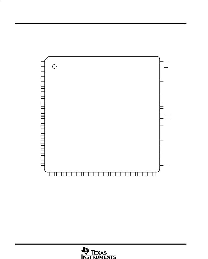
TMS320C5x, TMS320LC5x
DIGITAL SIGNAL PROCESSORS
SPRS030A ± APRIL 1995 ± REVISED APRIL 1996
TMS320LC57 PBK PACKAGE ( TOP VIEW )
V |
V |
V |
CLKOUT1 XF |
|
HOLDA BDX DX |
HD7 BFSX HD6 FSX HD5 |
CLKMD2 HD4 |
|
V |
V |
TDO V |
X1 X2/CLKIN |
|
CLKMD3 BR HD3 |
|
STRB |
|
W/R PS |
IS DS |
HD2 V |
V |
||||||||||||||||||||||||||||||||||||||||||
|
|
|
|
|
|||||||||||||||||||||||||||||||||||||||||||||||||||||||||||
DDC |
DDI |
DDI |
|
|
|
|
|
|
|
|
|
|
|
|
|
|
|
|
|
|
|
|
|
|
|
|
|
SSI |
SSI |
|
|
DDC |
|
|
|
|
|
|
|
|
|
|
|
|
|
|
|
|
|
|
|
|
|
|
SSC |
SSC |
|||||||
|
|
|
|
|
|
|
|
|
|
|
|
|
|
|
|
|
|
|
|
|
|
|
|
|
|
|
|
|
|
|
|
|
|
|
|
|
|
|
|
|
|
|
|
|
|
|
|
|
|||||||||||||||
|
|
|
|
|
|
|
|
|
|
|
|
|
|
|
|
|
|
|
|
|
|
|
|
|
|
|
|
|
|
|
|
|
|
|
|
|
|
|
|
|
|
|
|
|
|
|
|
|
|
|
|
|
|
|
|
|
|
|
|
|
|
|
|
|
|
|
|
|
|
|
|
|
|
|
|
|
|
|
|
|
|
|
|
|
|
|
|
|
|
|
|
|
|
|
|
|
|
|
|
|
|
|
|
|
|
|
|
|
|
|
|
|
|
|
|
|
|
|
|
|
|
|
|
|
|
|
|
|
|
|
|
|
|
|
|
|
|
|
|
|
|
|
|
|
|
|
|
|
|
|
|
|
|
|
|
|
|
|
|
|
|
|
|
|
|
|
|
|
|
|
|
|
|
|
|
|
|
|
|
|
|
|
|
|
|
|
|
|
|
|
|
128 127 126 125 124 123 122 121 120 119 118 117 116 115 114 113 112 111 110 109 108 107 106 105 104 103 102 101 100 99 98 97
|
|
HINT |
|
1 |
|
|
|
|
|
|
|
|
|
|
|
|
|
|
|
|
|
|
|
|
|
|
|
|
|
|
|
|
|
|
|
|
|
|
|
96 |
||||
EMU0 |
2 |
|
|
|
|
|
|
|
|
|
|
|
|
|
|
|
|
|
|
|
|
|
|
|
|
|
|
|
|
|
|
|
|
|
|
|
95 |
|||||||
3 |
|
|
|
|
|
|
|
|
|
|
|
|
|
|
|
|
|
|
|
|
|
|
|
|
|
|
|
|
|
|
|
|
|
|
|
94 |
||||||||
|
|
|
|
|
|
|
|
|
|
|
|
|
|
|
|
|
|
|
|
|
|
|
|
|
|
|
|
|
|
|
|
|
|
|
|
|
|
|
|
|
|
|||
EMU1 / OFF |
|
|
|
|
|
|
|
|
|
|
|
|
|
|
|
|
|
|
|
|
|
|
|
|
|
|
|
|
|
|
|
|
|
|
|
|||||||||
|
|
|
|
|
|
|
|
|
|
|
|
|
|
|
|
|
|
|
|
|
|
|
|
|
|
|
|
|
|
|
|
|
|
|
|
|
|
|||||||
|
VSSC |
4 |
|
|
|
|
|
|
|
|
|
|
|
|
|
|
|
|
|
|
|
|
|
|
|
|
|
|
|
|
|
|
|
|
|
|
|
93 |
||||||
|
VSSC |
5 |
|
|
|
|
|
|
|
|
|
|
|
|
|
|
|
|
|
|
|
|
|
|
|
|
|
|
|
|
|
|
|
|
|
|
|
92 |
||||||
|
TOUT |
6 |
|
|
|
|
|
|
|
|
|
|
|
|
|
|
|
|
|
|
|
|
|
|
|
|
|
|
|
|
|
|
|
|
|
|
|
91 |
||||||
BCLKX |
7 |
|
|
|
|
|
|
|
|
|
|
|
|
|
|
|
|
|
|
|
|
|
|
|
|
|
|
|
|
|
|
|
|
|
|
|
90 |
|||||||
|
CLKX |
8 |
|
|
|
|
|
|
|
|
|
|
|
|
|
|
|
|
|
|
|
|
|
|
|
|
|
|
|
|
|
|
|
|
|
|
|
89 |
||||||
VDDC |
9 |
|
|
|
|
|
|
|
|
|
|
|
|
|
|
|
|
|
|
|
|
|
|
|
|
|
|
|
|
|
|
|
|
|
|
|
88 |
|||||||
|
BFSR |
10 |
|
|
|
|
|
|
|
|
|
|
|
|
|
|
|
|
|
|
|
|
|
|
|
|
|
|
|
|
|
|
|
|
|
|
|
87 |
||||||
BCLKR |
11 |
|
|
|
|
|
|
|
|
|
|
|
|
|
|
|
|
|
|
|
|
|
|
|
|
|
|
|
|
|
|
|
|
|
|
|
86 |
|||||||
|
|
|
RS |
|
|
|
12 |
|
|
|
|
|
|
|
|
|
|
|
|
|
|
|
|
|
|
|
|
|
|
|
|
|
|
|
|
|
|
|
|
|
|
|
85 |
|
READY |
13 |
|
|
|
|
|
|
|
|
|
|
|
|
|
|
|
|
|
|
|
|
|
|
|
|
|
|
|
|
|
|
|
|
|
|
|
84 |
|||||||
|
|
|
|
|
14 |
|
|
|
|
|
|
|
|
|
|
|
|
|
|
|
|
|
|
|
|
|
|
|
|
|
|
|
|
|
|
|
|
|
|
|
83 |
|||
|
HOLD |
|
|
|
|
|
|
|
|
|
|
|
|
|
|
|
|
|
|
|
|
|
|
|
|
|
|
|
|
|
|
|
|
|
|
|
|
|
||||||
|
|
|
BIO |
|
15 |
|
|
|
|
|
|
|
|
|
|
|
|
|
|
|
|
|
|
|
|
|
|
|
|
|
|
|
|
|
|
|
|
|
|
|
82 |
|||
VDDC |
16 |
|
|
|
|
|
|
|
|
|
|
|
|
|
|
|
|
|
|
|
|
|
|
|
|
|
|
|
|
|
|
|
|
|
|
|
81 |
|||||||
VDDC |
17 |
|
|
|
|
|
|
|
|
|
|
|
|
|
|
|
|
|
|
|
|
|
|
|
|
|
|
|
|
|
|
|
|
|
|
|
80 |
|||||||
|
|
|
IAQ |
|
18 |
|
|
|
|
|
|
|
|
|
|
|
|
|
|
|
|
|
|
|
|
|
|
|
|
|
|
|
|
|
|
|
|
|
|
|
79 |
|||
|
TRST |
|
19 |
|
|
|
|
|
|
|
|
|
|
|
|
|
|
|
|
|
|
|
|
|
|
|
|
|
|
|
|
|
|
|
|
|
|
|
78 |
|||||
|
|
VSSI |
20 |
|
|
|
|
|
|
|
|
|
|
|
|
|
|
|
|
|
|
|
|
|
|
|
|
|
|
|
|
|
|
|
|
|
|
|
77 |
|||||
|
|
VSSI |
21 |
|
|
|
|
|
|
|
|
|
|
|
|
|
|
|
|
|
|
|
|
|
|
|
|
|
|
|
|
|
|
|
|
|
|
|
76 |
|||||
|
22 |
|
|
|
|
|
|
|
|
|
|
|
|
|
|
|
|
|
|
|
|
|
|
|
|
|
|
|
|
|
|
|
|
|
|
|
75 |
|||||||
MP / |
MC |
|
|
|
|
|
|
|
|
|
|
|
|
|
|
|
|
|
|
|
|
|
|
|
|
|
|
|
|
|
|
|
|
|
|
|
|
|||||||
|
|
|
D15 |
23 |
|
|
|
|
|
|
|
|
|
|
|
|
|
|
|
|
|
|
|
|
|
|
|
|
|
|
|
|
|
|
|
|
|
|
|
74 |
||||
|
|
|
D14 |
24 |
|
|
|
|
|
|
|
|
|
|
|
|
|
|
|
|
|
|
|
|
|
|
|
|
|
|
|
|
|
|
|
|
|
|
|
73 |
||||
|
|
|
D13 |
25 |
|
|
|
|
|
|
|
|
|
|
|
|
|
|
|
|
|
|
|
|
|
|
|
|
|
|
|
|
|
|
|
|
|
|
|
72 |
||||
|
|
|
D12 |
26 |
|
|
|
|
|
|
|
|
|
|
|
|
|
|
|
|
|
|
|
|
|
|
|
|
|
|
|
|
|
|
|
|
|
|
|
71 |
||||
|
|
|
D11 |
27 |
|
|
|
|
|
|
|
|
|
|
|
|
|
|
|
|
|
|
|
|
|
|
|
|
|
|
|
|
|
|
|
|
|
|
|
70 |
||||
|
|
|
D10 |
28 |
|
|
|
|
|
|
|
|
|
|
|
|
|
|
|
|
|
|
|
|
|
|
|
|
|
|
|
|
|
|
|
|
|
|
|
69 |
||||
|
|
|
D9 |
29 |
|
|
|
|
|
|
|
|
|
|
|
|
|
|
|
|
|
|
|
|
|
|
|
|
|
|
|
|
|
|
|
|
|
|
|
68 |
||||
|
|
|
D8 |
30 |
|
|
|
|
|
|
|
|
|
|
|
|
|
|
|
|
|
|
|
|
|
|
|
|
|
|
|
|
|
|
|
|
|
|
|
67 |
||||
VDDD |
31 |
|
|
|
|
|
|
|
|
|
|
|
|
|
|
|
|
|
|
|
|
|
|
|
|
|
|
|
|
|
|
|
|
|
|
|
66 |
|||||||
32 |
|
|
|
|
|
|
|
|
|
|
|
|
|
|
|
|
|
|
|
|
|
|
|
|
|
|
|
|
|
|
|
|
|
|
|
65 |
||||||||
VDDD |
|
|
|
|
|
|
|
|
|
|
|
|
|
|
|
|
|
|
|
|
|
|
|
|
|
|
|
|
|
|
|
|
|
|
|
|||||||||
|
|
|
|
|
|
|
|
|
|
|
|
|
|
|
|
|
|
|
|
|
|
|
|
|
|
|
|
|
|
|
|
|
|
|
|
|
|
|||||||
|
|
|
|
|
|
|
33 |
34 |
35 |
36 |
37 |
38 |
39 |
40 |
41 |
42 |
43 |
44 |
45 |
46 |
47 |
48 |
49 |
50 |
51 |
52 |
53 |
54 |
55 |
56 |
57 |
58 |
59 |
60 |
61 |
62 |
63 |
64 |
||||||
|
|
|
|
|
|
|
V |
V |
D7 |
D6 |
D5 |
D4 |
D3 |
D2 |
D1 |
D0 |
HCNTL0 |
TMS |
HCNTL1 |
V |
V |
TCK |
V |
V |
HR/W |
|
INT1 |
|
INT2 |
|
INT3 |
|
INT4 |
HBIL |
|
NMI DR |
BDR |
FSR |
CLKR |
V |
V |
|
HAS |
|
|
|
|
|
|
|
|
SSD |
SSD |
|
|
|
|
|
|
|
|
|
|
|
DDD |
DDD |
|
SSD |
SSD |
|
|
|
|
|
|
|
|
|
|
|
|
|
|
|
|
DDA |
DDA |
|
|
|
|
|
|
|
|
|
|
|
|
|
|
|
|
|
|
|
|
|
|
|
|
|
|
|
|
|
|
|
|
|
|
|
|
|
|
|
|
|
|
|
||||

 WE
WE

 HD1
HD1

 RD
RD

 HD0
HD0

 HRDY
HRDY

 VDDA
VDDA

 A15
A15

 A14
A14

 A13
A13

 A12
A12

 A11
A11
 A10
A10 
 CLKMD1
VSSA
VSSA 
 TDI
TDI

 HDS1
HDS1

 HDS2
HDS2

 VDDI
VDDI

 VDDI
VDDI

 A9
A9

 A8
A8

 A7
A7

 A6
A6

 A5
A5

 A4
A4

 A3
A3

 A2
A2

 A1
A1
 A0
A0 
 VSSA
VSSA

 HCS
HCS
6 |
POST OFFICE BOX 1443 •HOUSTON, TEXAS 77251±1443 |

TMS320C5x, TMS320LC5x
DIGITAL SIGNAL PROCESSORS
SPRS030A ± APRIL 1995 ± REVISED APRIL 1996
Pin Functions for the TMS320LC57 in the PBK Package
|
|
|
|
|
|
|
|
|
|
|
|
|
|
|
|
|
|
SIGNAL |
|
TYPE |
DESCRIPTION |
|
|||||||||
|
|
|
|
|
|
|
|
|
|
|
|
|
|
|
|
|
|
|
|
|
|
|
|
|
|
|
|
|
|
|
|
|
|
|
|
|
|
|
|
|
|
|
|
|
|
|
|
|
|
|
|
|
|
|
|
|
|
|
|
|
|
PARALLEL INTERFACE BUS |
|
|
|
|
|
|
|
|
|
|
|
|
|
|
|
|
|
|
|
|
|
|
|
|
|
|
|
|
|
|
|
|
|
|
A0 ± A15 |
|
I / O / Z |
16-bit external address bus (MSB: A15, LSB: A0) |
|
||||||||||||||||||||||||||
|
|
|
|
|
|
|
|
|
|
|
|
|
|
|
|
|
|
|
|
|
|
|
|
|
|
|
|
|
|
|
|
|
D0 ± D15 |
|
I / O / Z |
16-bit external data bus (MSB: D15, LSB: D0) |
|
||||||||||||||||||||||||||
|
|
|
|
|
|
|
|
|
|
|
|
|
|
|
|
|
|
|
|
|
|
|
|
|
|
|
|
|
|
|
|
|
|
|
|
|
|
|
|
|
|
|
|
|
|
|
|
|
|
|
|
|
|
|
|
|
|
|
|
|
O / Z |
Program, data, and I /O space select outputs, respectively |
|
|
PS, |
|
|
|
|
|
|
DS, |
|
|
|
IS |
|
|
|
|
|||||||||||||||
|
|
|
|
|
|
|
|
|
|
|
|
|
|
|
|
|
|
|
|
|
|
|
|
|
|
|
|
|
|||
|
|
|
|
|
|
|
|
|
|
|
|
|
|
|
|
|
|
|
|
|
|
|
|
|
|
|
|
|
I / O / Z |
Timing strobe for external cycles and external DMA |
|
|
STRB |
|
|
|
|
|
|
|
|
|
|
|
|||||||||||||||||||
|
|
|
|
|
|
|
|
|
|
|
|
|
|
|
|
|
|
|
|
|
|
|
|
|
|
|
|||||
|
R / |
|
|
|
|
|
|
|
|
|
|
|
|
|
|
|
|
|
|
|
|
|
|
|
|
|
|
|
I / O / Z |
Read/ write select for external cycles and external DMA |
|
|
W |
|
|
|
|
|
|
|
|
|
|
|
|
|
|||||||||||||||||
|
|
|
|
|
|
|
|
|
|
|
|
|
|
|
|
|
|
|
|
|
|
|
|
|
|
||||||
|
|
|
|
|
|
|
|
|
|
|
|
|
|
|
|
|
|
|
|
|
|
|
|
|
|
|
|
|
O / Z |
Read and write strobes, respectively, for external cycles |
|
|
RD, |
|
|
|
|
|
|
WE |
|
|
|
|
|
||||||||||||||||||
|
|
|
|
|
|
|
|
|
|
|
|
|
|
|
|
|
|
|
|
|
|
|
|
|
|||||||
|
READY |
|
|
|
|
I |
External bus ready/ wait-state control input |
|
|||||||||||||||||||||||
|
|
|
|
|
|
|
|
|
|
|
|
|
|
|
|
|
|
|
|
|
|
|
|
||||||||
|
|
|
|
|
|
|
|
|
|
|
|
|
|
|
|
|
|
|
|
|
|
|
|
|
|
|
|
|
I / O / Z |
Bus request. Arbitrates global memory and external DMA |
|
|
BR |
|
|
|
|
|
|
|
|
|
|
|
|
|
|
|
|
|
|
|
|
|
|||||||||
|
|
|
|
|
|
|
|
|
|
|
|
|
|
|
|
|
|
|
|
|
|
|
|
|
|
|
|
|
|
|
|
|
|
|
|
|
|
|
|
|
|
|
|
|
|
|
|
|
|
|
|
|
|
|
|
|
|
|
|
|
|
SYSTEM INTERFACE / CONTROL SIGNALS |
|
|
|
|
|
|
|
|
|
|
|
|
|
|
|
|
|
|
|
|
|
|
|
|
|
||||||||
|
RS |
|
|
|
|
|
|
|
|
|
|
|
|
|
|
|
|
|
|
|
|
I |
Reset. Initializes device and sets PC to zero |
|
|||||||
|
|
|
|
|
|
|
|
|
|
|
|
|
|
|
|
|
|
|
|
|
|
||||||||||
|
|
|
|
|
|
|
|
|
|
|
|
|
|
|
|
|
|
|
|
|
|
|
|
|
|
|
|
|
I |
Microprocessor/microcomputer mode select. Enables internal ROM |
|
|
MP/MC |
|
|
|
|
|
|
||||||||||||||||||||||||
|
|
|
|
|
|
|
|
|
|
|
|
|
|
|
|
|
|
|
|
|
|||||||||||
|
|
|
|
|
|
|
|
|
|
|
|
|
|
|
|
|
|
|
|
|
|
|
|
|
|
|
|
|
I |
Puts parallel I/ F bus in high-impedance state after current cycle |
|
|
HOLD |
|
|
|
|
|
|
|
|
|
|||||||||||||||||||||
|
|
|
|
|
|
|
|
|
|
|
|
|
|
|
|
|
|
|
|
||||||||||||
|
|
|
|
|
|
|
|
|
|
|
|
|
|
|
|
|
|
|
|
|
|
|
|
|
|
|
|
|
O / Z |
Hold acknowledge. Indicates external bus in hold state |
|
|
HOLDA |
|
|
|
|
|
|
||||||||||||||||||||||||
|
|
|
|
|
|
|
|
|
|
|
|
|
|
|
|
|
|
|
|
||||||||||||
|
XF |
|
|
|
|
O / Z |
External flag output. Set /cleared through software |
|
|||||||||||||||||||||||
|
|
|
|
|
|
|
|
|
|
|
|
|
|
|
|
|
|
|
|||||||||||||
|
|
|
|
|
|
|
|
|
|
|
|
|
|
|
|
|
|
|
|
|
|
|
|
|
|
|
|
|
I |
I /O branch input. Implements conditional branches |
|
|
BIO |
|
|
|
|
|
|
|
|
|
|
|
|
|
|
|
|
||||||||||||||
|
|
|
|
|
|
|
|
|
|
|
|
|
|
|
|
|
|
|
|||||||||||||
|
TOUT |
|
|
|
|
O / Z |
Timer output signal. Indicates output of internal timer |
|
|||||||||||||||||||||||
|
|
|
|
|
|
|
|
|
|
|
|
|
|
|
|
|
|
||||||||||||||
|
|
|
|
|
|
|
|
|
|
|
|
|
|
|
|
|
|
|
|
|
|
|
|
|
|
|
|
|
O / Z |
Instruction acquisition signal |
|
|
IAQ |
|
|
|
|
|
|
|
|
|
|
|
|
|
|
|
|||||||||||||||
|
|
|
|
|
|
|
|
|
|
|
|
|
|
± |
|
|
|
|
|
|
|
|
|
I |
External interrupt inputs |
|
|||||
|
INT1 |
|
INT4 |
|
|
|
|||||||||||||||||||||||||
|
|
|
|
|
|
|
|
|
|
|
|
|
|
|
|||||||||||||||||
|
|
|
|
|
|
|
|
|
|
|
|
|
|
|
|
|
|
|
|
|
|
|
|
|
|
|
|
|
I |
Nonmaskable external interrupt |
|
|
NMI |
|
|
|
|
|
|
|
|
|
|
|
|
||||||||||||||||||
|
|
|
|
|
|
|
|
|
|
|
|
|
|
|
|
|
|
|
|
|
|
|
|
|
|
|
|
|
|
|
|
|
|
|
|
|
|
|
|
|
|
|
|
|
|
|
|
|
|
|
|
|
|
|
|
|
|
|
|
|
|
SERIAL PORT INTERFACE |
|
|
|
|
|
|
|
|
|
|
|
|
|
|
|
|
|||||||||||||||||
|
DR |
|
|
|
|
I |
Serial receive-data input |
|
|||||||||||||||||||||||
|
|
|
|
|
|
|
|
|
|
|
|
|
|
|
|||||||||||||||||
|
DX |
|
|
|
|
O / Z |
Serial transmit-data output. In high-impedance state when not transmitting |
|
|||||||||||||||||||||||
|
|
|
|
|
|
|
|
|
|
|
|
|
|
|
|||||||||||||||||
|
CLKR |
|
|
|
|
I |
Serial receive-data clock input |
|
|||||||||||||||||||||||
|
|
|
|
|
|
|
|
|
|
|
|
|
|
|
|||||||||||||||||
|
CLKX |
|
|
|
|
I / O / Z |
Serial transmit-data clock. Internal or external source |
|
|||||||||||||||||||||||
|
|
|
|
|
|
|
|
|
|
|
|
|
|
|
|||||||||||||||||
|
FSR |
|
|
|
|
I |
Serial receive-frame-synchronization input |
|
|||||||||||||||||||||||
|
|
|
|
|
|
|
|
|
|
|
|
|
|
|
|||||||||||||||||
|
FSX |
|
|
|
|
I / O / Z |
Serial transmit-frame-synchronization signal. Internal or external source |
|
|||||||||||||||||||||||
|
|
|
|
|
|
|
|
|
|
|
|
|
|
|
|
|
|
|
|
|
|
|
|
|
|
|
|
|
|
|
|
|
|
|
|
|
|
|
|
|
|
|
|
|
|
|
|
|
|
|
|
|
|
|
|
|
|
|
|
|
|
HOST PORT INTERFACE (HPI) |
|
|
|
|
|
|
|
|
|
|
|
|
|||||||||||||||||||||
|
HCNTL0 |
|
I |
HPI mode control 1 |
|
||||||||||||||||||||||||||
|
|
|
|
|
|
|
|
|
|
|
|
||||||||||||||||||||
|
HCNTL1 |
|
I |
HPI mode control 2 |
|
||||||||||||||||||||||||||
|
|
|
|
|
|
|
|
|
|
|
|
|
|
||||||||||||||||||
|
|
|
|
|
|
|
|
|
|
|
|
|
|
|
|
|
|
|
|
|
|
|
|
|
|
|
|
|
O / Z |
Host interrupt |
|
|
HINT |
|
|
|
|
|
|
|
|
||||||||||||||||||||||
|
|
|
|
|
|
|
|
|
|
|
|
|
|||||||||||||||||||
|
|
|
|
|
|
|
|
|
|
|
|
|
|
|
|
|
|
|
|
|
|
|
|
|
|
|
|
|
I |
HPI data strobe 1 |
|
|
HDS1 |
|
|
|
|
|
|
|
|||||||||||||||||||||||
|
|
|
|
|
|
|
|
|
|
|
|
|
|||||||||||||||||||
|
|
|
|
|
|
|
|
|
|
|
|
|
|
|
|
|
|
|
|
|
|
|
|
|
|
|
|
|
I |
HPI data strobe 2 |
|
|
HDS2 |
|
|
|
|
|
|
|
|||||||||||||||||||||||
|
|
|
|
|
|
|
|
|
|
|
|||||||||||||||||||||
|
HR / |
|
|
|
|
|
|
|
|
|
|
|
|
|
|
|
|
|
|
|
I |
HPI read / write strobe |
|
||||||||
|
W |
|
|
|
|
|
|
||||||||||||||||||||||||
|
|
|
|
|
|
|
|
|
|
||||||||||||||||||||||
|
|
|
|
|
|
|
|
|
|
|
|
|
|
|
|
|
|
|
|
|
|
|
|
|
|
|
|
|
I |
HPI address strobe |
|
|
HAS |
|
|
|
|
|
|
|
|||||||||||||||||||||||
|
|
|
|
|
|
|
|
|
|
||||||||||||||||||||||
|
HRDY |
|
|
|
|
O / Z |
HPI ready signal |
|
|||||||||||||||||||||||
|
|
|
|
|
|
|
|
|
|||||||||||||||||||||||
|
|
|
|
|
|
|
|
|
|
|
|
|
|
|
|
|
|
|
|
|
|
|
|
|
|
|
|
|
I |
HPI chip select |
|
|
HCS |
|
|
|
|
|
|
||||||||||||||||||||||||
|
|
|
|
|
|
|
|
|
|||||||||||||||||||||||
|
HBIL |
|
|
|
|
I |
HPI byte identification input |
|
|||||||||||||||||||||||
|
|
|
|
|
|
||||||||||||||||||||||||||
|
HD0 ± HD7 |
|
I / O / Z |
HPI data bus |
|
||||||||||||||||||||||||||
LEGEND: |
|
|
|
||||||||||||||||||||||||||||
|
I = |
Input |
|
|
|
||||||||||||||||||||||||||
|
O = |
Output |
|
|
|
||||||||||||||||||||||||||
|
Z = |
High impedance |
|
|
|
||||||||||||||||||||||||||
|
|
|
|
|
|
|
|
|
|
|
|
|
|
|
|
|
|
|
|
|
|
|
|
|
|
|
|
|
|
|
|
|
|
|
|
|
|
|
|
|
|
|
|
|
|
|
|
|
|
|
|
|
|
|
|
|
|
|
|
|
|
|
|
POST OFFICE BOX 1443 •HOUSTON, TEXAS 77251±1443 |
7 |

TMS320C5x, TMS320LC5x
DIGITAL SIGNAL PROCESSORS
SPRS030A ± APRIL 1995 ± REVISED APRIL 1996
Pin Functions for the TMS320LC57 in the PBK Package (Continued)
|
|
SIGNAL |
|
TYPE |
DESCRIPTION |
|||
|
|
|
|
|
|
|
|
|
|
|
|
|
|
|
|
|
BUFFERED SERIAL PORT |
|
|
|
|
|
|
|
|
|
|
BDR |
|
|
|
I |
BSP receive data input |
||
|
|
|
|
|
|
|
|
|
|
BDX |
|
|
|
O / Z |
BSP transmit data output; in high-impedance state when not transmitting |
||
|
|
|
|
|
|
|
|
|
|
BCLKR |
|
|
|
I |
BSP receive-data clock input |
||
|
|
|
|
|
|
|
|
|
|
BCLKX |
|
|
|
I / O / Z |
BSP transmit-data clock; internal or external source |
||
|
|
|
|
|
|
|
|
|
|
BFSR |
|
|
|
I |
BSP receive frame-synchronization input |
||
|
|
|
|
|
|
|
|
|
|
BFSX |
|
|
|
I / O / Z |
BSP transmit frame-synchronization signal; internal or external source |
||
|
|
|
|
|
|
|
|
|
|
|
|
|
|
|
|
|
EMULATION/JTAG INTERFACE |
|
|
|
|
|
|
|
|
|
|
TDI |
|
|
|
I |
JTAG-test-port scan data input |
||
|
|
|
|
|
|
|
|
|
|
TDO |
|
|
|
O / Z |
JTAG-test-port scan data output |
||
|
|
|
|
|
|
|
|
|
|
TMS |
|
|
|
I |
JTAG-test-port mode select input |
||
|
|
|
|
|
|
|
|
|
|
TCK |
|
|
|
I |
JTAG-port clock input |
||
|
|
|
|
|
|
|
|
|
|
|
|
|
|
|
|
I |
JTAG-port reset (with pull-down resistor). Disables JTAG when low |
|
TRST |
|
|
|
|
|
||
|
|
|
|
|
|
|
|
|
|
EMU0 |
|
|
|
I / O / Z |
Emulation control 0. Reserved for emulation use |
||
|
|
|
|
|
||||
|
EMU1/ |
|
|
|
|
I / O / Z |
Emulation control 1. Puts outputs in high-impedance state when low |
|
|
OFF |
|
|
|||||
|
|
|
|
|
|
|
|
|
|
|
|
|
|
|
|
|
CLOCK GENERATION AND CONTROL |
|
|
|
|
|
|
|
||
|
X1 |
|
|
|
O |
Oscillator output |
||
|
|
|
|
|
||||
|
X2 / CLKIN |
|
I |
Clock input |
||||
|
|
|
|
|
||||
|
CLKMD1, CLKMD2, |
|
I |
Clock-mode select inputs |
||||
|
CLKMD3 |
|
||||||
|
|
|
|
|||||
|
|
|
|
|
||||
|
CLKOUT1 |
|
O / Z |
Device system-clock output |
||||
|
|
|
|
|
|
|
|
|
|
|
|
|
|
|
|
|
POWER SUPPLY CONNECTIONS |
|
|
|
|
|
|
|
||
|
VDDA |
|
|
|
S |
Supply connection, address-bus output |
||
|
VDDD |
|
|
|
S |
Supply connection, data-bus output |
||
|
VDDC |
|
|
|
S |
Supply connection, control output |
||
|
VDDI |
|
|
|
S |
Supply connection, internal logic |
||
|
VSSA |
|
|
|
S |
Supply connection, address-bus output |
||
|
VSSD |
|
|
|
S |
Supply connection, data-bus output |
||
|
VSSC |
|
|
|
S |
Supply connection, control output |
||
|
VSSI |
|
|
|
S |
Supply connection, internal logic |
||
LEGEND: |
|
|
||||||
|
I = |
Input |
|
|
||||
|
O = |
Output |
|
|
||||
|
S = |
Supply |
|
|
||||
|
Z = |
High impedance |
|
|
||||
8 |
POST OFFICE BOX 1443 •HOUSTON, TEXAS 77251±1443 |

TMS320C5x, TMS320LC5x
DIGITAL SIGNAL PROCESSORS
SPRS030A ± APRIL 1995 ± REVISED APRIL 1996
TMS320C51, TMS320LC51, TMS320C52, TMS320LC52, TMS320C53S, TMS320LC53S, TMS320LC56
PZ PACKAGE
( TOP VIEW )
|
|
|
|
|
|
|
|
|
|
|
V |
V |
|
V |
CLKOUT1 |
XF |
|
HOLDA ² ² ² ² CLKMD2 |
|
V |
|
V |
|
TDO |
|
V X1 |
CLKIN/X2 |
² BR STRB W/R PS IS |
|
DS |
|
V |
|
|
|
|
|
||||||||||||||||||||||||||||
|
|
|
|
|
|
|
|
|
|
|
|
|
|
|
|
|
|
|
|
|
|
|
|
||||||||||||||||||||||||||||||||||||||||||
|
|
|
|
|
|
|
|
|
|
|
DDC |
DDI |
|
DDI |
|
|
|
|
|
|
|
|
|
|
|
|
|
|
|
|
|
SSI |
|
SSI |
|
|
|
DDC |
|
|
|
|
|
|
|
|
|
|
|
|
|
|
|
|
SSC |
|
|
|
|
|
|||||
|
|
|
|
|
|
|
|
|
|
|
|
|
|
|
|
|
|
|
|
|
|
|
|
|
|
|
|
|
|
|
|
|
|
|
|
|
|
|
|
|
|
|
|
|
|
|
|
|
|
|
|
|
|
||||||||||||
|
|
|
|
|
|
|
|
|
|
|
|
|
|
|
|
|
|
|
|
|
|
|
|
|
|
|
|
|
|
|
|
|
|
|
|
|
|
|
|
|
|
|
|
|
|
|
|
|
|
|
|
|
|
|
|
|
|
|
|
|
|
|
|
|
|
|
|
|
|
|
|
|
|
|
|
|
|
|
|
|
|
|
|
|
|
|
|
|
|
|
|
|
|
|
|
|
|
|
|
|
|
|
|
|
|
|
|
|
|
|
|
|
|
|
|
|
|
|
|
|
|
|
|
|
|
|
|
|
|
|
|
|
|
|
|
|
|
|
|
|
|
|
|
|
|
|
|
|
|
|
|
|
|
|
|
|
|
|
|
|
|
|
|
|
|
|
|
|
|
|
|
|
|
|
|
|
|
|
|
|
|
|
|
|
|
|
|
|
|
|
|
|
|
|
|
|
|
|
|
|
|
|
|
|
|
100 99 98 97 |
96 95 94 93 92 91 90 89 88 |
87 86 85 84 83 82 81 80 79 78 |
77 76 |
|
|
|
|
|
|
||||||||||||||||||||||||||||||||||||||||||||||||
|
EMU0 |
|
1 |
|
|
|
|
|
|
|
|
|
|
|
|
|
|
|
|
|
|
|
|
|
|
|
|
|
|
|
|
|
|
|
|
|
|
|
|
|
|
|
|
|
|
|
|
|
|
|
|
75 |
|
|
|
||||||||||
|
|
|
|
|
|
|
|
|
|
|
|
|
|
|
|
|
|
|
|
|
|
|
|
|
|
|
|
|
|
|
|
|
|
|
|
|
|
|
|
|
|
|
|
|
|
|
|
|
|
|
|
WE |
|
||||||||||||
|
|
|
|
|
|
|
|
|
2 |
|
|
|
|
|
|
|
|
|
|
|
|
|
|
|
|
|
|
|
|
|
|
|
|
|
|
|
|
|
|
|
|
|
|
|
|
|
|
|
|
|
|
|
|
|
|
|
|
74 |
|
|
|
|
|
||
EMU1/ |
OFF |
|
|
|
|
|
|
|
|
|
|
|
|
|
|
|
|
|
|
|
|
|
|
|
|
|
|
|
|
|
|
|
|
|
|
|
|
|
|
|
|
|
|
|
|
|
|
|
|
|
|
|
RD |
|
|
||||||||||
|
VSSC |
|
3 |
|
|
|
|
|
|
|
|
|
|
|
|
|
|
|
|
|
|
|
|
|
|
|
|
|
|
|
|
|
|
|
|
|
|
|
|
|
|
|
|
|
|
|
|
|
|
|
|
73 |
|
|
VDDA |
||||||||||
|
|
|
|
|
|
|
|
|
|
|
|
|
|
|
|
|
|
|
|
|
|
|
|
|
|
|
|
|
|
|
|
|
|
|
|
|
|
|
|
|
|
|
|
|
|
|
|
||||||||||||||||||
|
|
|
|
|
|
|
|
|
|
|
|
|
|
|
|
|
|
|
|
|
|
|
|
|
|
|
|
|
|
|
|
|
|
|
|
|
|
|
|
|
|
|
|
|
|
|
|
||||||||||||||||||
|
TOUT |
|
4 |
|
|
|
|
|
|
|
|
|
|
|
|
|
|
|
|
|
|
|
|
|
|
|
|
|
|
|
|
|
|
|
|
|
|
|
|
|
|
|
|
|
|
|
|
|
|
|
|
72 |
|
|
A15 |
||||||||||
² |
|
|
|
|
5 |
|
|
|
|
|
|
|
|
|
|
|
|
|
|
|
|
|
|
|
|
|
|
|
|
|
|
|
|
|
|
|
|
|
|
|
|
|
|
|
|
|
|
|
|
|
|
|
|
71 |
|
|
A14 |
||||||||
|
|
|
|
|
|
|
|
|
|
|
|
|
|
|
|
|
|
|
|
|
|
|
|
|
|
|
|
|
|
|
|
|
|
|
|
|
|
|
|
|
|
|
|
|
|
|
|
|
|
||||||||||||||||
² |
|
|
|
|
6 |
|
|
|
|
|
|
|
|
|
|
|
|
|
|
|
|
|
|
|
|
|
|
|
|
|
|
|
|
|
|
|
|
|
|
|
|
|
|
|
|
|
|
|
|
|
|
|
|
70 |
|
|
A13 |
||||||||
|
|
|
|
|
|
|
|
|
|
|
|
|
|
|
|
|
|
|
|
|
|
|
|
|
|
|
|
|
|
|
|
|
|
|
|
|
|
|
|
|
|
|
|
|
|
|
|
|
|
||||||||||||||||
² |
|
|
|
|
7 |
|
|
|
|
|
|
|
|
|
|
|
|
|
|
|
|
|
|
|
|
|
|
|
|
|
|
|
|
|
|
|
|
|
|
|
|
|
|
|
|
|
|
|
|
|
|
|
|
69 |
|
|
A12 |
||||||||
|
|
|
|
|
|
|
|
|
|
|
|
|
|
|
|
|
|
|
|
|
|
|
|
|
|
|
|
|
|
|
|
|
|
|
|
|
|
|
|
|
|
|
|
|
|
|
|
|
|
||||||||||||||||
² |
|
|
|
|
8 |
|
|
|
|
|
|
|
|
|
|
|
|
|
|
|
|
|
|
|
|
|
|
|
|
|
|
|
|
|
|
|
|
|
|
|
|
|
|
|
|
|
|
|
|
|
|
|
|
68 |
|
|
A11 |
||||||||
|
|
|
|
|
|
|
|
|
|
|
|
|
|
|
|
|
|
|
|
|
|
|
|
|
|
|
|
|
|
|
|
|
|
|
|
|
|
|
|
|
|
|
|
|
|
|
|
|
|
||||||||||||||||
|
|
|
|
|
|
|
|
|
9 |
|
|
|
|
|
|
|
|
|
|
|
|
|
|
|
|
|
|
|
|
|
|
|
|
|
|
|
|
|
|
|
|
|
|
|
|
|
|
|
|
|
|
|
|
|
|
|
|
67 |
|
|
A10 |
||||
|
|
|
|
RS |
|
|
|
|
|
|
|
|
|
|
|
|
|
|
|
|
|
|
|
|
|
|
|
|
|
|
|
|
|
|
|
|
|
|
|
|
|
|
|
|
|
|
|
|
|
|
|
|
|
|
|
|
|
|
|||||||
READY |
|
10 |
|
|
|
|
|
|
|
|
|
|
|
|
|
|
|
|
|
|
|
|
|
|
|
|
|
|
|
|
|
|
|
|
|
|
|
|
|
|
|
|
|
|
|
|
|
|
|
66 |
|
|
CLKMD1 |
||||||||||||
|
|
|
|
|
|
|
|
|
|
|
|
|
|
|
|
|
|
|
|
|
|
|
|
|
|
|
|
|
|
|
|
|
|
|
|
|
|
|
|
|
|
|
|
|
|
|
|||||||||||||||||||
|
|
|
|
|
|
|
|
|
11 |
|
|
|
|
|
|
|
|
|
|
|
|
|
|
|
|
|
|
|
|
|
|
|
|
|
|
|
|
|
|
|
|
|
|
|
|
|
|
|
|
|
|
|
|
|
|
|
65 |
|
|
VSSA |
|||||
|
HOLD |
|
|
|
|
|
|
|
|
|
|
|
|
|
|
|
|
|
|
|
|
|
|
|
|
|
|
|
|
|
|
|
|
|
|
|
|
|
|
|
|
|
|
|
|
|
|
|
|
|
|||||||||||||||
|
|
|
|
|
|
|
|
|
|
|
|
|
|
|
|
|
|
|
|
|
|
|
|
|
|
|
|
|
|
|
|
|
|
|
|
|
|
|
|
|
|
|
|
|
|
|
|
|
|
||||||||||||||||
|
|
|
BIO |
|
|
|
12 |
|
|
|
|
|
|
|
|
|
|
|
|
|
|
|
|
|
|
|
|
|
|
|
|
|
|
|
|
|
|
|
|
|
|
|
|
|
|
|
|
|
|
|
|
|
|
|
64 |
|
|
VSSA |
|||||||
|
|
|
|
|
|
|
|
|
|
|
|
|
|
|
|
|
|
|
|
|
|
|
|
|
|
|
|
|
|
|
|
|
|
|
|
|
|
|
|
|
|
|
|
|
|
|
|
|
|
|
|
|
|||||||||||||
|
|
TRST |
|
|
13 |
|
|
|
|
|
|
|
|
|
|
|
|
|
|
|
|
|
|
|
|
|
|
|
|
|
|
|
|
|
|
|
|
|
|
|
|
|
|
|
|
|
|
|
|
|
|
|
63 |
|
|
TDI |
|||||||||
|
|
V |
|
14 |
|
|
|
|
|
|
|
|
|
|
|
|
|
|
|
|
|
|
|
|
|
|
|
|
|
|
|
|
|
|
|
|
|
|
|
|
|
|
|
|
|
|
|
|
|
|
|
62 |
|
|
VDDI |
||||||||||
|
|
|
|
|
|
|
|
|
|
|
|
|
|
|
|
|
|
|
|
|
|
|
|
|
|
|
|
|
|
|
|
|
|
|
|
|
|
|
|
|
|
|
|
|
|
|
|
|
|||||||||||||||||
|
|
|
SSI |
|
15 |
|
|
|
|
|
|
|
|
|
|
|
|
|
|
|
|
|
|
|
|
|
|
|
|
|
|
|
|
|
|
|
|
|
|
|
|
|
|
|
|
|
|
|
|
|
|
|
61 |
|
|
A9 |
|||||||||
|
|
VSSI |
|
|
|
|
|
|
|
|
|
|
|
|
|
|
|
|
|
|
|
|
|
|
|
|
|
|
|
|
|
|
|
|
|
|
|
|
|
|
|
|
|
|
|
|
|
|
|
|
|
|
|||||||||||||
|
|
|
|
|
|
|
|
|
|
|
|
|
|
|
|
|
|
|
|
|
|
|
|
|
|
|
|
|
|
|
|
|
|
|
|
|
|
|
|
|
|
|
|
|
|
|
|
|
|||||||||||||||||
MP/ MC |
|
16 |
|
|
|
|
|
|
|
|
|
|
|
|
|
|
|
|
|
|
|
|
|
|
|
|
|
|
|
|
|
|
|
|
|
|
|
|
|
|
|
|
|
|
|
|
|
|
|
60 |
|
|
A8 |
||||||||||||
|
|
D15 |
|
17 |
|
|
|
|
|
|
|
|
|
|
|
|
|
|
|
|
|
|
|
|
|
|
|
|
|
|
|
|
|
|
|
|
|
|
|
|
|
|
|
|
|
|
|
|
|
|
|
59 |
|
|
A7 |
||||||||||
|
|
|
|
|
|
|
|
|
|
|
|
|
|
|
|
|
|
|
|
|
|
|
|
|
|
|
|
|
|
|
|
|
|
|
|
|
|
|
|
|
|
|
|
|
|
|
|
|
|||||||||||||||||
|
|
|
D14 |
|
18 |
|
|
|
|
|
|
|
|
|
|
|
|
|
|
|
|
|
|
|
|
|
|
|
|
|
|
|
|
|
|
|
|
|
|
|
|
|
|
|
|
|
|
|
|
|
|
|
58 |
|
|
A6 |
|||||||||
|
|
|
|
|
|
|
|
|
|
|
|
|
|
|
|
|
|
|
|
|
|
|
|
|
|
|
|
|
|
|
|
|
|
|
|
|
|
|
|
|
|
|
|
|
|
|
|
|
|
||||||||||||||||
|
|
D13 |
|
19 |
|
|
|
|
|
|
|
|
|
|
|
|
|
|
|
|
|
|
|
|
|
|
|
|
|
|
|
|
|
|
|
|
|
|
|
|
|
|
|
|
|
|
|
|
|
|
|
57 |
|
|
A5 |
||||||||||
|
|
|
|
|
|
|
|
|
|
|
|
|
|
|
|
|
|
|
|
|
|
|
|
|
|
|
|
|
|
|
|
|
|
|
|
|
|
|
|
|
|
|
|
|
|
|
|
|
|||||||||||||||||
|
|
D12 |
|
20 |
|
|
|
|
|
|
|
|
|
|
|
|
|
|
|
|
|
|
|
|
|
|
|
|
|
|
|
|
|
|
|
|
|
|
|
|
|
|
|
|
|
|
|
|
|
|
|
56 |
|
|
A4 |
||||||||||
|
|
|
|
|
|
|
|
|
|
|
|
|
|
|
|
|
|
|
|
|
|
|
|
|
|
|
|
|
|
|
|
|
|
|
|
|
|
|
|
|
|
|
|
|
|
|
|
|
|||||||||||||||||
|
|
|
D11 |
|
21 |
|
|
|
|
|
|
|
|
|
|
|
|
|
|
|
|
|
|
|
|
|
|
|
|
|
|
|
|
|
|
|
|
|
|
|
|
|
|
|
|
|
|
|
|
|
|
|
55 |
|
|
A3 |
|||||||||
|
|
|
|
|
|
|
|
|
|
|
|
|
|
|
|
|
|
|
|
|
|
|
|
|
|
|
|
|
|
|
|
|
|
|
|
|
|
|
|
|
|
|
|
|
|
|
|
|
|
||||||||||||||||
|
|
D10 |
|
22 |
|
|
|
|
|
|
|
|
|
|
|
|
|
|
|
|
|
|
|
|
|
|
|
|
|
|
|
|
|
|
|
|
|
|
|
|
|
|
|
|
|
|
|
|
|
|
|
54 |
|
|
A2 |
||||||||||
|
|
|
|
|
|
|
|
|
|
|
|
|
|
|
|
|
|
|
|
|
|
|
|
|
|
|
|
|
|
|
|
|
|
|
|
|
|
|
|
|
|
|
|
|
|
|
|
|
|||||||||||||||||
|
|
|
|
D9 |
|
23 |
|
|
|
|
|
|
|
|
|
|
|
|
|
|
|
|
|
|
|
|
|
|
|
|
|
|
|
|
|
|
|
|
|
|
|
|
|
|
|
|
|
|
|
|
|
|
|
53 |
|
|
A1 |
||||||||
|
|
|
|
|
|
|
|
|
|
|
|
|
|
|
|
|
|
|
|
|
|
|
|
|
|
|
|
|
|
|
|
|
|
|
|
|
|
|
|
|
|
|
|
|
|
|
|
|
|
|
|||||||||||||||
|
|
|
|
D8 |
|
24 |
|
|
|
|
|
|
|
|
|
|
|
|
|
|
|
|
|
|
|
|
|
|
|
|
|
|
|
|
|
|
|
|
|
|
|
|
|
|
|
|
|
|
|
|
|
|
|
52 |
|
|
A0 |
||||||||
|
|
|
|
|
|
|
|
|
|
|
|
|
|
|
|
|
|
|
|
|
|
|
|
|
|
|
|
|
|
|
|
|
|
|
|
|
|
|
|
|
|
|
|
|
|
|
|
|
|
|
|||||||||||||||
|
VDDD |
|
25 |
|
|
|
|
|
|
|
|
|
|
|
|
|
|
|
|
|
|
|
|
|
|
|
|
|
|
|
|
|
|
|
|
|
|
|
|
|
|
|
|
|
|
|
|
|
|
|
51 |
|
|
VSSA |
|||||||||||
|
|
|
|
|
|
|
|
|
|
|
|
|
|
|
|
|
|
|
|
|
|
|
|
|
|
|
|
|
|
|
|
|
|
|
|
|
|
|
|
|
|
|
|
|
|
|
|
||||||||||||||||||
|
|
|
|
|
|
|
|
|
26 |
|
27 28 |
|
29 30 |
|
31 32 33 34 35 36 |
37 38 |
39 40 41 42 |
43 44 45 46 47 48 |
49 50 |
|
|
|
|
|
|
||||||||||||||||||||||||||||||||||||||||
|
|
|
|
|
|
|
|
|
|
|
|
|
|
|
|
|
|
|
|
|
|
|
|
|
|
|
|
|
|
|
|
|
|
|
|
|
|
|
|
|
|
|
|
|
|
|
|
|
|
|
|
|
|
|
|
|
|
|
|
|
|
|
|
|
|
|
|
|
|
|
|
|
|
|
|
|
SSD |
SSD |
|
|
|
|
|
|
|
|
|
|
|
|
|
|
|
|
|
|
|
|
DDD |
|
|
|
SSD |
SSD |
|
|
|
|
|
|
|
|
|
|
|
|
|
|
|
|
|
|
DDA |
|
|
|
|
|
|||
|
|
|
|
|
|
|
|
|
|
|
|
|
|
|
|
|
|
|
|
|
|
|
|
|
|
|
|
|
|
|
|
|
|
|
|
|
|
|
|
|
|
|
|
|
|
|
|
|
|
|
|
|
|
|
|
|
|||||||||
|
|
|
|
|
|
|
|
|
|
|
V |
V |
|
D7 |
D6 |
D5 D4 D3 D2 D1 D0 TMS |
|
|
|
TCK |
V |
|
|
|
INT1 |
INT2 |
INT3 INT4 NMI ² ² ² |
² |
|
|
|
|
|
|
|||||||||||||||||||||||||||||||
|
|
|
|
|
|
|
|
|
|
|
|
|
|
|
|
V |
|
|
V |
|
|
|
|
|
|
|
|
|
|
|
|
|
|
|
|
|
V |
|
|
|
|
|
|||||||||||||||||||||||
NOTE: |
NC = No connect (These pins are reserved.) |
|
|
|
|
|
|
|
|
|
|
|
|
|
|
|
|
|
|
|
|
|
|
|
|||||||||||||||||||||||||||||||||||||||||
² See Table 2 for device-specific pinouts. |
|
|
|
|
|
|
|
|
|
|
|
|
|
|
|
|
|
|
|
|
|
|
|
|
|
|
|
|
|
|
|
|
|
||||||||||||||||||||||||||||||||
Table 2. Device-Specific Pinouts for the PZ Package
PIN |
'C51, 'LC51 |
'C52, 'LC52 |
'C53S, 'LC53S |
'LC56³ |
5 |
TCLKX |
VSSI |
CLKX2 |
BCLKX |
6§ |
CLKX |
CLKX |
CLKX1 |
CLKX |
7 |
TFSR / TADD |
VSSI |
FSR2 |
BFSR |
8 |
TCLKR |
VSSI |
CLKR2 |
BCLKR |
46§ |
DR |
DR |
DR1 |
DR |
47 |
TDR |
VSSI |
DR2 |
BDR |
48§ |
FSR |
FSR |
FSR1 |
FSR |
49§ |
CLKR |
CLKR |
CLKR1 |
CLKR |
83 |
CLKIN2 |
CLKIN2 |
CLKIN2 |
CLKMD3 |
|
|
|
|
|
91§ |
FSX |
FSX |
FSX1 |
FSX |
92 |
TFSX / TFRM |
VSSI |
FSX2 |
BFSX |
93§ |
DX |
DX |
DX1 |
DX |
94 |
TDX |
NC |
DX2 |
BDX |
³ Pin names beginning with ªBº indicate signals on the buffered serial port (BSP). § No functional change
POST OFFICE BOX 1443 •HOUSTON, TEXAS 77251±1443 |
9 |

TMS320C5x, TMS320LC5x
DIGITAL SIGNAL PROCESSORS
SPRS030A ± APRIL 1995 ± REVISED APRIL 1996
|
|
|
|
|
|
|
|
|
|
|
|
|
|
|
|
|
|
|
|
|
|
|
Pin Functions for Devices in the PZ Package |
|
|
|
|
|
|
|
|
|
|
|
|
|
|
|
|
SIGNAL |
TYPE |
|
DESCRIPTION |
||||||
|
|
|
|
|
|
|
|
|
|
|
|
|
|
|
|
|
|
|
|
|
|
|
|
|
|
|
|
|
|
|
|
|
|
|
|
|
|
|
|
|
|
|
|
|
|
|
|
|
PARALLEL INTERFACE BUS |
|
|
|
|
|
|
|
|
|
|
|
|
|
|
|
|
|
|
|
|
|
|
|
|
|
|
A0 ± A15 |
I / O / Z |
|
16-bit external address bus (MSB: A15, LSB: A0) |
||||||||||||||||||||
|
|
|
|
|
|
|
|
|
|
|
|
|
|
|
|
|
|
|
|
|
|
|
|
|
|
D0 ± D15 |
I / O / Z |
|
16-bit external data bus (MSB: D15, LSB: D0) |
||||||||||||||||||||
|
|
|
|
|
|
|
|
|
|
|
|
|
|
|
|
|
|
|
|
|
|
|
|
|
|
|
|
|
|
|
|
|
|
|
|
|
|
|
|
|
|
|
|
|
|
|
O / Z |
|
Program, data, and I /O space select outputs, respectively |
|
PS, |
|
|
|
|
|
DS, |
|
|
|
|
IS |
|
|
|
|||||||||
|
|
|
|
|
|
|
|
|
|
|
|
|
|
|
|
|
|
|
|
|
|
|||
|
|
|
|
|
|
|
|
|
|
|
|
|
|
|
|
|
|
|
|
|
|
I / O / Z |
|
Timing strobe for external cycles and external DMA |
|
STRB |
|
|
|
|
|
|
|
|
|
|
|||||||||||||
|
|
|
|
|
|
|
|
|
|
|
|
|
|
|
|
|
|
|
|
|||||
|
R / |
|
|
|
|
|
|
|
|
|
|
|
|
|
|
|
|
|
|
|
|
I / O / Z |
|
Read/ write select for external cycles and external DMA |
|
W |
|
|
|
|
|
|
|
|
|
|
|||||||||||||
|
|
|
|
|
|
|
|
|
|
|
|
|
|
|
|
|
|
|
||||||
|
|
|
|
|
|
|
|
|
|
|
|
|
|
|
|
|
|
|
|
|
|
O / Z |
|
Read and write strobes, respectively, for external cycles |
|
RD, |
|
|
|
|
WE |
|
|
|
|
|
|||||||||||||
|
|
|
|
|
|
|
|
|
|
|
|
|
|
|
|
|
|
|||||||
|
READY |
|
|
|
|
I |
|
External bus ready/ wait-state control input |
||||||||||||||||
|
|
|
|
|
|
|
|
|
|
|
|
|
|
|
|
|
||||||||
|
|
|
|
|
|
|
|
|
|
|
|
|
|
|
|
|
|
|
|
|
|
I / O / Z |
|
Bus request. Arbitrates global memory and external DMA |
|
BR |
|
|
|
|
|
|
|
|
|
|
|
|
|
|
|||||||||
|
|
|
|
|
|
|
|
|
|
|
|
|
|
|
|
|
|
|
|
|
|
|
|
|
|
|
|
|
|
|
|
|
|
|
|
|
|
|
|
|
|
|
|
|
|
|
|
|
SYSTEM INTERFACE / CONTROL SIGNALS |
|
|
|
|
|
|
|
|
|
|
|
|
|
|
|
|
|
||||||||
|
RS |
|
|
|
|
|
|
|
|
|
|
|
|
|
I |
|
Reset. Initializes device and sets PC to zero |
|||||||
|
|
|
|
|
|
|
|
|
|
|
|
|
|
|
||||||||||
|
|
|
|
|
|
|
|
|
|
|
|
|
|
|
|
|
|
|
|
|
|
I |
|
Microprocessor/microcomputer mode select. Enables internal ROM |
|
MP/MC |
|
|
|
|
|
|
|||||||||||||||||
|
|
|
|
|
|
|
|
|
|
|
|
|
|
|||||||||||
|
|
|
|
|
|
|
|
|
|
|
|
|
|
|
|
|
|
|
|
|
|
I |
|
Puts parallel I/ F bus in high-impedance state after current cycle |
|
HOLD |
|
|
|
|
|
|
|
|
|||||||||||||||
|
|
|
|
|
|
|
|
|
|
|
|
|
||||||||||||
|
|
|
|
|
|
|
|
|
|
|
|
|
|
|
|
|
|
|
|
|
|
O / Z |
|
Hold acknowledge. Indicates external bus in hold state |
|
HOLDA |
|
|
|
|
|
|
|||||||||||||||||
|
|
|
|
|
|
|
|
|
|
|
|
|
||||||||||||
|
XF |
|
|
|
|
O / Z |
|
External flag output. Set /cleared through software |
||||||||||||||||
|
|
|
|
|
|
|
|
|
|
|
|
|||||||||||||
|
|
|
|
|
|
|
|
|
|
|
|
|
|
|
|
|
|
|
|
|
|
I |
|
I /O branch input. Implements conditional branches |
|
BIO |
|
|
|
|
|
|
|
|
|
||||||||||||||
|
|
|
|
|
|
|
|
|
|
|
|
|||||||||||||
|
TOUT |
|
|
|
|
O / Z |
|
Timer output signal. Indicates output of internal timer |
||||||||||||||||
|
|
|
|
|
|
|
|
|||||||||||||||||
|
|
|
|
|
|
|
|
|
|
± |
|
|
|
|
|
|
|
|
I |
|
External interrupt inputs |
|||
|
INT1 |
INT4 |
|
|
||||||||||||||||||||
|
|
|
|
|
|
|
|
|
|
|
|
|
|
|
|
|
|
|
|
|
|
I |
|
Nonmaskable external interrupt |
|
NMI |
|
|
|
|
|
|
|||||||||||||||||
|
|
|
|
|
|
|
|
|
|
|
|
|
|
|
|
|
|
|
|
|
|
|
|
|
|
|
|
|
|
|
|
|
|
|
|
|
|
|
|
|
|
|
|
|
|
|
|
|
SERIAL PORT INTERFACE |
|
|
|
|
|
||||||||||||||||||||
|
DR, DR1, DR2 |
I |
|
Serial receive-data input |
||||||||||||||||||||
|
|
|
|
|
||||||||||||||||||||
|
DX, DX1, DX2 |
O / Z |
|
Serial transmit-data output. In high-impedance state when not transmitting |
||||||||||||||||||||
|
|
|
|
|
||||||||||||||||||||
|
CLKR, CLKR1, CLKR2 |
I |
|
Serial receive-data clock input |
||||||||||||||||||||
|
|
|
|
|
||||||||||||||||||||
|
CLKX, CLKX1, CLKX2 |
I / O / Z |
|
Serial transmit-data clock. Internal or external source |
||||||||||||||||||||
|
|
|
|
|
||||||||||||||||||||
|
FSR, FSR1, FSR2 |
I |
|
Serial receive-frame-synchronization input |
||||||||||||||||||||
|
|
|
|
|
||||||||||||||||||||
|
FSX, FSX1, FSX2 |
I / O / Z |
|
Serial transmit-frame-synchronization signal. Internal or external source |
||||||||||||||||||||
|
|
|
|
|
|
|
|
|
|
|
|
|
|
|
|
|
|
|
|
|
|
|
|
|
|
|
|
|
|
|
|
|
|
|
|
|
|
|
|
|
|
|
|
|
|
|
|
|
BUFFERED SERIAL PORT (BSP) (SEE NOTE 1) |
|
|
|
|
|
|
|
|
|
||||||||||||||||
|
BDR |
|
|
|
|
I |
|
BSP receive data input |
||||||||||||||||
|
|
|
|
|
|
|
|
|
||||||||||||||||
|
BDX |
|
|
|
|
O / Z |
|
BSP transmit data output; in high-impedance state when not transmitting |
||||||||||||||||
|
|
|
|
|
|
|
|
|
||||||||||||||||
|
BCLKR |
|
|
|
|
I |
|
BSP receive-data clock input |
||||||||||||||||
|
|
|
|
|
|
|
|
|
||||||||||||||||
|
BCLKX |
|
|
|
|
I / O / Z |
|
BSP transmit-data clock; internal or external source |
||||||||||||||||
|
|
|
|
|
|
|
|
|
||||||||||||||||
|
BFSR |
|
|
|
|
I |
|
BSP receive frame-synchronization input |
||||||||||||||||
|
|
|
|
|
|
|
|
|
||||||||||||||||
|
BFSX |
|
|
|
|
I / O / Z |
|
BSP transmit frame-synchronization signal; internal or external source |
||||||||||||||||
LEGEND: |
|
|
|
|||||||||||||||||||||
|
I = |
Input |
|
|
|
|||||||||||||||||||
|
O = |
Output |
|
|
|
|||||||||||||||||||
|
Z = |
High impedance |
|
|
|
|||||||||||||||||||
NOTE 1: 'LC56 devices only
10 |
POST OFFICE BOX 1443 •HOUSTON, TEXAS 77251±1443 |
|
|
|
|
|
|
|
|
TMS320C5x, TMS320LC5x |
|
|
|
|
|
|
|
|
|
DIGITAL SIGNAL PROCESSORS |
|
|
|
|
|
|
|
|
|
SPRS030A ± APRIL 1995 ± REVISED APRIL 1996 |
|
|
|
|
|
|
|
|
|
|
|
|
|
|
|
|
|
|
Pin Functions for Devices in the PZ Package (Continued) |
||
|
|
|
|
|
|
|
|
|
|
|
|
SIGNAL |
|
TYPE |
DESCRIPTION |
|
|||
|
|
|
|
|
|
|
|
|
|
|
|
|
|
|
|
|
|
TDM SERIAL PORT INTERFACE |
|
|
|
|
|
|
|
|
|
|
|
|
TDR |
|
|
|
I |
TDM serial receive-data input |
|
||
|
|
|
|
|
|
|
|
|
|
|
TDX |
|
|
|
O / Z |
TDM serial transmit-data output. In high-impedance state when not transmitting |
|
||
|
|
|
|
|
|
|
|
|
|
|
TCLKR |
|
|
|
I |
TDM serial receive-data clock input |
|
||
|
|
|
|
|
|
|
|
|
|
|
TCLKX |
|
|
|
I / O / Z |
TDM serial transmit-data clock. Internal or external source |
|
||
|
|
|
|
|
|
|
|
|
|
|
TFSR / TADD |
|
I / O / Z |
TDM serial receive-frame-synchronization input. In the TDM mode, TFSR / TADD is used to output / |
|
||||
|
|
input the address of the port |
|
||||||
|
|
|
|
|
|
|
|
|
|
|
|
|
|
|
|
|
|
|
|
|
TFSX / TFRM |
|
I |
TDM serial transmit-frame-synchronization signal. Internal or external source. In the TDM mode, |
|
||||
|
|
TFSX / TFRM becomes TFRM, the TDM frame sync. |
|
||||||
|
|
|
|
|
|
|
|
|
|
|
|
|
|
|
|
|
|
|
|
|
|
|
|
|
|
|
|
EMULATION/JTAG INTERFACE |
|
|
|
|
|
|
|
|
|
|
|
|
TDI |
|
|
|
I |
JTAG-test-port scan data input |
|
||
|
|
|
|
|
|
|
|
|
|
|
TDO |
|
|
|
O / Z |
JTAG-test-port scan data output |
|
||
|
|
|
|
|
|
|
|
|
|
|
TMS |
|
|
|
I |
JTAG-test-port mode select input |
|
||
|
|
|
|
|
|
|
|
|
|
|
TCK |
|
|
|
I |
JTAG-port clock input |
|
||
|
|
|
|
|
|
|
|
|
|
|
|
|
|
|
|
|
I |
JTAG-port reset (with pull-down resistor). Disables JTAG when low |
|
|
TRST |
|
|
|
|
|
|
||
|
|
|
|
|
|
|
|
|
|
|
EMU0 |
|
|
|
I / O / Z |
Emulation control 0. Reserved for emulation use |
|
||
|
|
|
|
|
|
||||
|
EMU1/ |
|
|
|
|
I / O / Z |
Emulation control 1. Puts outputs in high-impedance state when low |
|
|
|
OFF |
|
|
|
|||||
|
|
|
|
|
|
|
|
|
|
|
|
|
|
|
|
|
|
CLOCK GENERATION AND CONTROL (SEE NOTE 2) |
|
|
|
|
|
|
|
|
|
||
|
X1 |
|
|
|
O |
Oscillator output |
|
||
|
|
|
|
|
|
||||
|
X2 / CLKIN |
|
I |
Clock/oscillator input (PLL clock input for 'C56) |
|
||||
|
|
|
|
|
|
|
|
||
|
CLKIN2 |
|
|
|
I |
Clock input (PLL clock input for 'C50, 'C51, 'C52, 'C53, 'C53S) |
|
||
|
|
|
|
|
|
||||
|
CLKMD1, CLKMD2, |
|
I |
Clock-mode select inputs |
|
||||
|
CLKMD3 |
|
|
||||||
|
|
|
|
|
|||||
|
|
|
|
|
|
||||
|
CLKOUT1 |
|
O / Z |
Device system-clock output |
|
||||
|
|
|
|
|
|
|
|
|
|
|
|
|
|
|
|
|
|
POWER SUPPLY CONNECTIONS |
|
|
|
|
|
|
|
|
|
||
|
VDDA |
|
|
|
S |
Supply connection, address-bus output |
|
||
|
VDDD |
|
|
|
S |
Supply connection, data-bus output |
|
||
|
VDDC |
|
|
|
S |
Supply connection, control output |
|
||
|
VDDI |
|
|
|
S |
Supply connection, internal logic |
|
||
|
VSSA |
|
|
|
S |
Supply connection, address-bus output |
|
||
|
VSSD |
|
|
|
S |
Supply connection, data-bus output |
|
||
|
VSSC |
|
|
|
S |
Supply connection, control output |
|
||
|
VSSI |
|
|
|
S |
Supply connection, internal logic |
|
||
LEGEND: |
|
|
|
||||||
|
I = |
Input |
|
|
|
||||
|
O = |
Output |
|
|
|
||||
|
S = |
Supply |
|
|
|
||||
|
Z = |
High impedance |
|
|
|
||||
NOTE 2: CLKIN2 pin is replaced by CLKMD3 pin on 'LC56 devices.
POST OFFICE BOX 1443 •HOUSTON, TEXAS 77251±1443 |
11 |
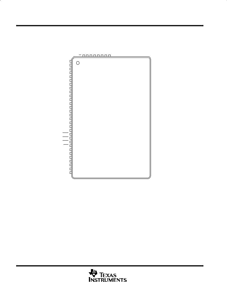
TMS320C5x, TMS320LC5x
DIGITAL SIGNAL PROCESSORS
SPRS030A ± APRIL 1995 ± REVISED APRIL 1996
TMS320C52, TMS320LC52
PJ PACKAGE
( TOP VIEW )
D8
VDDD VSSD
VSSD D7
D6
D5
D4
D3
D2
D1
D0
TMS
VDDD
VDDD
TCK
VSSD
VSSD INT1
INT2
INT3
INT4
NMI
DR
VSSI FSR
CLKR
VDDA
VSSA A0
|
|
|
D10 |
|
|
|
D12 |
|
D13 |
|
D14 |
|
D15 |
|
MC |
|
SSI |
|
D9 |
|
|
D11 |
|
|
|
|
|
MP/ |
|
||||||||
|
|
|
|
|
|
|
|
V |
||||||||||
|
|
|
|
|
|
|
|
|
|
|
|
|
|
|
|
|
|
|
|
|
|
|
|
|
|
|
|
|
|
|
|
|
|
|
|
|
|
100 99 |
98 |
97 |
96 |
95 |
94 |
93 |
92 |
|||||||||||
1 |
|
|
|
|
|
|
|
|
|
|
|
|
|
|
|
|
|
|
2 |
|
|
|
|
|
|
|
|
|
|
|
|
|
|
|
|
|
|
3 |
|
|
|
|
|
|
|
|
|
|
|
|
|
|
|
|
|
|
4 |
|
|
|
|
|
|
|
|
|
|
|
|
|
|
|
|
|
|
5 |
|
|
|
|
|
|
|
|
|
|
|
|
|
|
|
|
|
|
6 |
|
|
|
|
|
|
|
|
|
|
|
|
|
|
|
|
|
|
7 |
|
|
|
|
|
|
|
|
|
|
|
|
|
|
|
|
|
|
8 |
|
|
|
|
|
|
|
|
|
|
|
|
|
|
|
|
|
|
9 |
|
|
|
|
|
|
|
|
|
|
|
|
|
|
|
|
|
|
10 |
|
|
|
|
|
|
|
|
|
|
|
|
|
|
|
|
|
|
11 |
|
|
|
|
|
|
|
|
|
|
|
|
|
|
|
|
|
|
12 |
|
|
|
|
|
|
|
|
|
|
|
|
|
|
|
|
|
|
13 |
|
|
|
|
|
|
|
|
|
|
|
|
|
|
|
|
|
|
14 |
|
|
|
|
|
|
|
|
|
|
|
|
|
|
|
|
|
|
15 |
|
|
|
|
|
|
|
|
|
|
|
|
|
|
|
|
|
|
16 |
|
|
|
|
|
|
|
|
|
|
|
|
|
|
|
|
|
|
17 |
|
|
|
|
|
|
|
|
|
|
|
|
|
|
|
|
|
|
18 |
|
|
|
|
|
|
|
|
|
|
|
|
|
|
|
|
|
|
19 |
|
|
|
|
|
|
|
|
|
|
|
|
|
|
|
|
|
|
20 |
|
|
|
|
|
|
|
|
|
|
|
|
|
|
|
|
|
|
21 |
|
|
|
|
|
|
|
|
|
|
|
|
|
|
|
|
|
|
22 |
|
|
|
|
|
|
|
|
|
|
|
|
|
|
|
|
|
|
23 |
|
|
|
|
|
|
|
|
|
|
|
|
|
|
|
|
|
|
24 |
|
|
|
|
|
|
|
|
|
|
|
|
|
|
|
|
|
|
25 |
|
|
|
|
|
|
|
|
|
|
|
|
|
|
|
|
|
|
26 |
|
|
|
|
|
|
|
|
|
|
|
|
|
|
|
|
|
|
27 |
|
|
|
|
|
|
|
|
|
|
|
|
|
|
|
|
|
|
28 |
|
|
|
|
|
|
|
|
|
|
|
|
|
|
|
|
|
|
29 |
|
|
|
|
|
|
|
|
|
|
|
|
|
|
|
|
|
|
30 |
|
|
|
|
|
|
|
|
|
|
|
|
|
|
|
|
|
|
31 |
32 |
33 |
34 |
35 |
36 |
37 |
38 |
39 |
||||||||||
|
|
|
|
|
|
|
|
|
|
|
|
|
|
|
|
|
|
|
|
|
|
|
|
|
|
|
|
|
|
|
|
|
|
|
|
|
|
|
A1 |
|
A2 |
|
A3 |
|
A4 |
|
A5 |
|
A6 |
|
A7 |
|
A8 |
|
A9 |
|
|
TRST |
BIO |
HOLD |
|
READY |
RS |
V |
V |
|
CLKX |
V |
|
TOUT |
V |
|
|
|
|
|
|
|
|
|
|
|
|||||||||||||
|
|
|
|
|
|
|
|
|
|
|
|
SSI |
|
SSI |
|
|
|
SSI |
|
|
|
SSC |
|
|
|
|
|
|
|
|
|
|
|
|||||
|
|
|
|
|
|
|
|
|
|
|
|
|
|
|
|
|
|
|
|
|
|
|
|
|
|
|
|
|
|
|||||||||
|
|
|
|
|
|
|
|
|
|
|
|
|
|
|
|
|
|
|
|
|
|
|
|
|
|
|
|
|
|
|
|
|
|
|
|
|
|
|
|
|
|
|
|
|
|
|
|
|
|
|
|
|
|
|
|
|
|
|
|
|
|
|
|
|
|
|
|
|
|
|
|
|
|
|
|
|
|
91 |
90 |
89 |
88 |
87 |
86 |
85 |
84 |
83 |
82 |
81 |
|
|
|
|
|
|
|
|
|
|
|
|
||||||||||||||||
|
|
|
|
|
|
|
|
|
|
|
|
|
|
|
|
|
|
|
|
|
|
|
|
80 |
|
|
EMU1/ OFF |
|||||||||||
|
|
|
|
|
|
|
|
|
|
|
|
|
|
|
|
|
|
|
|
|
|
|
|
|
||||||||||||||
|
|
|
|
|
|
|
|
|
|
|
|
|
|
|
|
|
|
|
|
|
|
|
|
79 |
|
|
EMU0 |
|||||||||||
|
|
|
|
|
|
|
|
|
|
|
|
|
|
|
|
|
|
|
|
|
|
|
|
|
|
|||||||||||||
|
|
|
|
|
|
|
|
|
|
|
|
|
|
|
|
|
|
|
|
|
|
|
|
|
||||||||||||||
|
|
|
|
|
|
|
|
|
|
|
|
|
|
|
|
|
|
|
|
|
|
|
|
78 |
|
|
VDDC |
|||||||||||
|
|
|
|
|
|
|
|
|
|
|
|
|
|
|
|
|
|
|
|
|
|
|
|
|
|
|||||||||||||
|
|
|
|
|
|
|
|
|
|
|
|
|
|
|
|
|
|
|
|
|
|
|
|
|
||||||||||||||
|
|
|
|
|
|
|
|
|
|
|
|
|
|
|
|
|
|
|
|
|
|
|
|
77 |
|
|
VDDC |
|||||||||||
|
|
|
|
|
|
|
|
|
|
|
|
|
|
|
|
|
|
|
|
|
|
|
|
|
||||||||||||||
|
|
|
|
|
|
|
|
|
|
|
|
|
|
|
|
|
|
|
|
|
|
|
|
76 |
|
|
VDDI |
|||||||||||
|
|
|
|
|
|
|
|
|
|
|
|
|
|
|
|
|
|
|
|
|
|
|
|
|
||||||||||||||
|
|
|
|
|
|
|
|
|
|
|
|
|
|
|
|
|
|
|
|
|
|
|
|
75 |
|
|
VDDI |
|||||||||||
|
|
|
|
|
|
|
|
|
|
|
|
|
|
|
|
|
|
|
|
|
|
|
|
|
||||||||||||||
|
|
|
|
|
|
|
|
|
|
|
|
|
|
|
|
|
|
|
|
|
|
|
|
74 |
|
|
CLKOUT1 |
|||||||||||
|
|
|
|
|
|
|
|
|
|
|
|
|
|
|
|
|
|
|
|
|
|
|
|
|
||||||||||||||
|
|
|
|
|
|
|
|
|
|
|
|
|
|
|
|
|
|
|
|
|
|
|
|
73 |
|
|
XF |
|||||||||||
|
|
|
|
|
|
|
|
|
|
|
|
|
|
|
|
|
|
|
|
|
|
|
|
|
|
|||||||||||||
|
|
|
|
|
|
|
|
|
|
|
|
|
|
|
|
|
|
|
|
|
|
|
|
|
||||||||||||||
|
|
|
|
|
|
|
|
|
|
|
|
|
|
|
|
|
|
|
|
|
|
|
|
72 |
|
|
|
HOLDA |
||||||||||
|
|
|
|
|
|
|
|
|
|
|
|
|
|
|
|
|
|
|
|
|
|
|
|
|
||||||||||||||
|
|
|
|
|
|
|
|
|
|
|
|
|
|
|
|
|
|
|
|
|
|
|
|
71 |
|
|
NC |
|||||||||||
|
|
|
|
|
|
|
|
|
|
|
|
|
|
|
|
|
|
|
|
|
|
|
|
|
|
|||||||||||||
|
|
|
|
|
|
|
|
|
|
|
|
|
|
|
|
|
|
|
|
|
|
|
|
|
||||||||||||||
|
|
|
|
|
|
|
|
|
|
|
|
|
|
|
|
|
|
|
|
|
|
|
|
70 |
|
|
DX |
|||||||||||
|
|
|
|
|
|
|
|
|
|
|
|
|
|
|
|
|
|
|
|
|
|
|
|
|
|
|||||||||||||
|
|
|
|
|
|
|
|
|
|
|
|
|
|
|
|
|
|
|
|
|
|
|
|
|
||||||||||||||
|
|
|
|
|
|
|
|
|
|
|
|
|
|
|
|
|
|
|
|
|
|
|
|
69 |
|
|
VSSI |
|||||||||||
|
|
|
|
|
|
|
|
|
|
|
|
|
|
|
|
|
|
|
|
|
|
|
|
|
||||||||||||||
|
|
|
|
|
|
|
|
|
|
|
|
|
|
|
|
|
|
|
|
|
|
|
|
|
||||||||||||||
|
|
|
|
|
|
|
|
|
|
|
|
|
|
|
|
|
|
|
|
|
|
|
|
68 |
|
|
FSX |
|||||||||||
|
|
|
|
|
|
|
|
|
|
|
|
|
|
|
|
|
|
|
|
|
|
|
|
|
||||||||||||||
|
|
|
|
|
|
|
|
|
|
|
|
|
|
|
|
|
|
|
|
|
|
|
|
67 |
|
|
CLKMD2 |
|||||||||||
|
|
|
|
|
|
|
|
|
|
|
|
|
|
|
|
|
|
|
|
|
|
|
|
|
||||||||||||||
|
|
|
|
|
|
|
|
|
|
|
|
|
|
|
|
|
|
|
|
|
|
|
|
|
||||||||||||||
|
|
|
|
|
|
|
|
|
|
|
|
|
|
|
|
|
|
|
|
|
|
|
|
66 |
|
|
VSSI |
|||||||||||
|
|
|
|
|
|
|
|
|
|
|
|
|
|
|
|
|
|
|
|
|
|
|
|
|
||||||||||||||
|
|
|
|
|
|
|
|
|
|
|
|
|
|
|
|
|
|
|
|
|
|
|
|
|
||||||||||||||
|
|
|
|
|
|
|
|
|
|
|
|
|
|
|
|
|
|
|
|
|
|
|
|
65 |
|
|
VSSI |
|||||||||||
|
|
|
|
|
|
|
|
|
|
|
|
|
|
|
|
|
|
|
|
|
|
|
|
|
|
|||||||||||||
|
|
|
|
|
|
|
|
|
|
|
|
|
|
|
|
|
|
|
|
|
|
|
|
64 |
|
|
TDO |
|||||||||||
|
|
|
|
|
|
|
|
|
|
|
|
|
|
|
|
|
|
|
|
|
|
|
|
|
|
|||||||||||||
|
|
|
|
|
|
|
|
|
|
|
|
|
|
|
|
|
|
|
|
|
|
|
|
63 |
|
|
VDDC |
|||||||||||
|
|
|
|
|
|
|
|
|
|
|
|
|
|
|
|
|
|
|
|
|
|
|
|
|
||||||||||||||
|
|
|
|
|
|
|
|
|
|
|
|
|
|
|
|
|
|
|
|
|
|
|
|
|
|
|||||||||||||
|
|
|
|
|
|
|
|
|
|
|
|
|
|
|
|
|
|
|
|
|
|
|
|
62 |
|
|
X1 |
|||||||||||
|
|
|
|
|
|
|
|
|
|
|
|
|
|
|
|
|
|
|
|
|
|
|
|
|
|
|||||||||||||
|
|
|
|
|
|
|
|
|
|
|
|
|
|
|
|
|
|
|
|
|
|
|
|
61 |
|
|
X2 / CLKIN |
|||||||||||
|
|
|
|
|
|
|
|
|
|
|
|
|
|
|
|
|
|
|
|
|
|
|
|
|
||||||||||||||
|
|
|
|
|
|
|
|
|
|
|
|
|
|
|
|
|
|
|
|
|
|
|
|
|
|
|||||||||||||
|
|
|
|
|
|
|
|
|
|
|
|
|
|
|
|
|
|
|
|
|
|
|
|
60 |
|
|
CLKIN2 |
|||||||||||
|
|
|
|
|
|
|
|
|
|
|
|
|
|
|
|
|
|
|
|
|
|
|
|
|
||||||||||||||
|
|
|
|
|
|
|
|
|
|
|
|
|
|
|
|
|
|
|
|
|
|
|
|
|
||||||||||||||
|
|
|
|
|
|
|
|
|
|
|
|
|
|
|
|
|
|
|
|
|
|
|
|
59 |
|
|
|
BR |
|
|
|
|
|
|||||
|
|
|
|
|
|
|
|
|
|
|
|
|
|
|
|
|
|
|
|
|
|
|
|
|
|
|||||||||||||
|
|
|
|
|
|
|
|
|
|
|
|
|
|
|
|
|
|
|
|
|
|
|
|
|
|
|
|
|
|
|
|
|
|
|||||
|
|
|
|
|
|
|
|
|
|
|
|
|
|
|
|
|
|
|
|
|
|
|
|
58 |
|
|
|
STRB |
|
|||||||||
|
|
|
|
|
|
|
|
|
|
|
|
|
|
|
|
|
|
|
|
|
|
|
|
|
|
|||||||||||||
|
|
|
|
|
|
|
|
|
|
|
|
|
|
|
|
|
|
|
|
|
|
|
|
|
|
|
|
|
|
|
|
|||||||
|
|
|
|
|
|
|
|
|
|
|
|
|
|
|
|
|
|
|
|
|
|
|
|
57 |
|
|
R/ |
W |
|
|||||||||
|
|
|
|
|
|
|
|
|
|
|
|
|
|
|
|
|
|
|
|
|
|
|
|
|
|
|||||||||||||
|
|
|
|
|
|
|
|
|
|
|
|
|
|
|
|
|
|
|
|
|
|
|
|
|
|
|
|
|
|
|
||||||||
|
|
|
|
|
|
|
|
|
|
|
|
|
|
|
|
|
|
|
|
|
|
|
|
56 |
|
|
|
PS |
|
|
|
|||||||
|
|
|
|
|
|
|
|
|
|
|
|
|
|
|
|
|
|
|
|
|
|
|
|
|
||||||||||||||
|
|
|
|
|
|
|
|
|
|
|
|
|
|
|
|
|
|
|
|
|
|
|
|
|
|
|
|
|
|
|||||||||
|
|
|
|
|
|
|
|
|
|
|
|
|
|
|
|
|
|
|
|
|
|
|
|
55 |
|
|
|
IS |
|
|
|
|||||||
|
|
|
|
|
|
|
|
|
|
|
|
|
|
|
|
|
|
|
|
|
|
|
|
|
||||||||||||||
|
|
|
|
|
|
|
|
|
|
|
|
|
|
|
|
|
|
|
|
|
|
|
|
54 |
|
|
|
DS |
|
|
|
|||||||
|
|
|
|
|
|
|
|
|
|
|
|
|
|
|
|
|
|
|
|
|
|
|
|
|
||||||||||||||
|
|
|
|
|
|
|
|
|
|
|
|
|
|
|
|
|
|
|
|
|
|
|
|
53 |
|
|
VSSC |
|||||||||||
|
|
|
|
|
|
|
|
|
|
|
|
|
|
|
|
|
|
|
|
|
|
|
|
|
||||||||||||||
|
|
|
|
|
|
|
|
|
|
|
|
|
|
|
|
|
|
|
|
|
|
|
|
|
||||||||||||||
|
|
|
|
|
|
|
|
|
|
|
|
|
|
|
|
|
|
|
|
|
|
|
|
52 |
|
|
|
WE |
|
|||||||||
|
|
|
|
|
|
|
|
|
|
|
|
|
|
|
|
|
|
|
|
|
|
|
|
|
||||||||||||||
|
|
|
|
|
|
|
|
|
|
|
|
|
|
|
|
|
|
|
|
|
|
|
|
|
|
|
|
|||||||||||
|
|
|
|
|
|
|
|
|
|
|
|
|
|
|
|
|
|
|
|
|
|
|
|
51 |
|
|
|
RD |
|
|||||||||
40 |
41 |
42 |
43 |
44 |
45 |
46 |
47 |
48 |
49 |
50 |
|
|
|
|
|
|
|
|
|
|
|
|
||||||||||||||||
|
|
|
|
|
|
|
|
|
|
|
|
|
|
|
|
|
|
|
|
|
|
|
|
|
|
|
|
|
|
|
|
|||||||
|
|
|
|
|
|
|
|
|
|
|
|
|
|
|
|
|
|
|
|
|
|
|
|
|
|
|
|
|
|
|
|
|
|
|
|
|
|
|
|
V |
TDI |
V |
|
CLKMD1 |
A10 |
|
A11 |
|
A12 |
|
A13 |
|
A14 |
|
A15 |
V |
|
|
|
|
|
|
|
|
|
|
|
||||||||||
|
DDI |
|
|
SSA |
|
|
|
|
|
|
|
|
|
|
|
|
|
|
|
|
|
|
DDA |
|
|
|
|
|
|
|
|
|
|
|
||||
NOTE: NC = No connect (These pins are reserved.)
12 |
POST OFFICE BOX 1443 •HOUSTON, TEXAS 77251±1443 |

TMS320C5x, TMS320LC5x
DIGITAL SIGNAL PROCESSORS
SPRS030A ± APRIL 1995 ± REVISED APRIL 1996
Pin Functions for the TMS320C52, TMS320LC52 in the PJ Package
|
|
|
|
|
|
|
|
|
|
|
|
|
SIGNAL |
|
TYPE |
DESCRIPTION |
||||||||||
|
|
|
|
|
|
|
|
|
|
|
|
|
|
|
|
|
|
|
|
|
|
|
|
|
|
|
|
|
|
|
|
|
|
|
|
|
|
|
|
|
|
|
|
|
|
|
|
|
|
|
|
|
PARALLEL INTERFACE BUS |
|
|
|
|
|
|
|
|
|
|
|
|
|
|
|
|
|
|
|
|
|
|
|
|
|
|
|
|
A0 ± A15 |
|
I / O / Z |
16-bit external address bus (MSB: A15, LSB: A0) |
||||||||||||||||||||||
|
|
|
|
|
|
|
|
|
|
|
|
|
|
|
|
|
|
|
|
|
|
|
|
|
|
|
|
D0 ± D15 |
|
I / O / Z |
16-bit external data bus (MSB: D15, LSB: D0) |
||||||||||||||||||||||
|
|
|
|
|
|
|
|
|
|
|
|
|
|
|
|
|
|
|
|
|
|
|
|
|
|
|
|
|
|
|
|
|
|
|
|
|
|
|
|
|
|
|
|
|
|
|
|
|
|
|
|
O / Z |
Program, data, and I /O space select outputs, respectively |
|
PS, |
|
|
|
|
|
DS, |
|
|
|
|
IS |
|
|
|
|
||||||||||
|
|
|
|
|
|
|
|
|
|
|
|
|
|
|
|
|
|
|
|
|
|
|
|
|||
|
|
|
|
|
|
|
|
|
|
|
|
|
|
|
|
|
|
|
|
|
|
|
|
|
I / O / Z |
Timing strobe for external cycles and external DMA |
|
STRB |
|
|
|
|
|
|
|
|
|
|
|
||||||||||||||
|
|
|
|
|
|
|
|
|
|
|
|
|
|
|
|
|
|
|
|
|
|
|||||
|
R / |
|
|
|
|
|
|
|
|
|
|
|
|
|
|
|
|
|
|
|
|
|
|
|
I / O / Z |
Read/ write select for external cycles and external DMA |
|
W |
|
|
|
|
|
|
|
|
|
|
|
|
|||||||||||||
|
|
|
|
|
|
|
|
|
|
|
|
|
|
|
|
|
|
|
|
|
||||||
|
|
|
|
|
|
|
|
|
|
|
|
|
|
|
|
|
|
|
|
|
|
|
|
|
O / Z |
Read and write strobes, respectively, for external cycles |
|
RD, |
|
|
|
|
WE |
|
|
|
|
|
|||||||||||||||
|
|
|
|
|
|
|
|
|
|
|
|
|
|
|
|
|
|
|
|
|||||||
|
READY |
|
|
|
|
|
I |
External bus ready/ wait-state control input |
||||||||||||||||||
|
|
|
|
|
|
|
|
|
|
|
|
|
|
|
|
|
|
|
||||||||
|
|
|
|
|
|
|
|
|
|
|
|
|
|
|
|
|
|
|
|
|
|
|
|
|
I / O / Z |
Bus request. Arbitrates global memory and external DMA |
|
BR |
|
|
|
|
|
|
|
|
|
|
|
|
|
|
|
|
|||||||||
|
|
|
|
|
|
|
|
|
|
|
|
|
|
|
|
|
|
|
|
|
|
|
|
|
|
|
|
|
|
|
|
|
|
|
|
|
|
|
|
|
|
|
|
|
|
|
|
|
|
|
|
|
SYSTEM INTERFACE / CONTROL SIGNALS |
|
|
|
|
|
|
|
|
|
|
|
|
|
|
|
|
|
|
|
||||||||
|
RS |
|
|
|
|
|
|
|
|
|
|
|
|
|
|
|
|
I |
Reset. Initializes device and sets PC to zero |
|||||||
|
|
|
|
|
|
|
|
|
|
|
|
|
|
|
|
|
||||||||||
|
|
|
|
|
|
|
|
|
|
|
|
|
|
|
|
|
|
|
|
|
|
|
|
|
I |
Microprocessor/microcomputer mode select. Enables internal ROM |
|
MP/MC |
|
|
|
|
|
|
|||||||||||||||||||
|
|
|
|
|
|
|
|
|
|
|
|
|
|
|
|
|||||||||||
|
|
|
|
|
|
|
|
|
|
|
|
|
|
|
|
|
|
|
|
|
|
|
|
|
I |
Puts parallel I/ F bus in high-impedance state after current cycle |
|
HOLD |
|
|
|
|
|
|
|
|
|
||||||||||||||||
|
|
|
|
|
|
|
|
|
|
|
|
|
|
|
||||||||||||
|
|
|
|
|
|
|
|
|
|
|
|
|
|
|
|
|
|
|
|
|
|
|
|
|
O / Z |
Hold acknowledge. Indicates external bus in hold state |
|
HOLDA |
|
|
|
|
|
|
|||||||||||||||||||
|
|
|
|
|
|
|
|
|
|
|
|
|
|
|
||||||||||||
|
XF |
|
|
|
|
|
O / Z |
External flag output. Set /cleared through software |
||||||||||||||||||
|
|
|
|
|
|
|
|
|
|
|
|
|
|
|||||||||||||
|
|
|
|
|
|
|
|
|
|
|
|
|
|
|
|
|
|
|
|
|
|
|
|
|
I |
I /O branch input. Implements conditional branches |
|
BIO |
|
|
|
|
|
|
|
|
|
|
|
||||||||||||||
|
|
|
|
|
|
|
|
|
|
|
|
|
|
|||||||||||||
|
TOUT |
|
|
|
|
|
O / Z |
Timer output signal. Indicates output of internal timer |
||||||||||||||||||
|
|
|
|
|
|
|
|
|
|
|
||||||||||||||||
|
|
|
|
|
|
|
|
|
|
± |
|
|
|
|
|
|
|
|
|
|
I |
External interrupt inputs |
||||
|
INT1 |
INT4 |
|
|
|
|||||||||||||||||||||
|
|
|
|
|
|
|
|
|
|
|
|
|
|
|
|
|
|
|
|
|
|
|
|
|
I |
Nonmaskable external interrupt |
|
NMI |
|
|
|
|
|
|
|
|
|||||||||||||||||
|
|
|
|
|
|
|
|
|
|
|
|
|
|
|
|
|
|
|
|
|
|
|
|
|
|
|
|
|
|
|
|
|
|
|
|
|
|
|
|
|
|
|
|
|
|
|
|
|
|
|
|
|
SERIAL PORT INTERFACE |
|
|
|
|
|
|
|
|
|
|
|
||||||||||||||||
|
DR |
|
|
|
|
|
I |
Serial receive-data input |
||||||||||||||||||
|
|
|
|
|
|
|
|
|
|
|
||||||||||||||||
|
DX |
|
|
|
|
|
O / Z |
Serial transmit-data output. In high-impedance state when not transmitting |
||||||||||||||||||
|
|
|
|
|
|
|
|
|
|
|
||||||||||||||||
|
CLKR |
|
|
|
|
|
I |
Serial receive-data clock input |
||||||||||||||||||
|
|
|
|
|
|
|
|
|
|
|
||||||||||||||||
|
CLKX |
|
|
|
|
|
I / O / Z |
Serial transmit-data clock. Internal or external source |
||||||||||||||||||
|
|
|
|
|
|
|
|
|
|
|
||||||||||||||||
|
FSR |
|
|
|
|
|
I |
Serial receive-frame-synchronization input |
||||||||||||||||||
|
|
|
|
|
|
|
|
|
|
|
||||||||||||||||
|
FSX |
|
|
|
|
|
I / O / Z |
Serial transmit-frame-synchronization signal. Internal or external source |
||||||||||||||||||
|
|
|
|
|
|
|
|
|
|
|
|
|
|
|
|
|
|
|
|
|
|
|
|
|
|
|
|
|
|
|
|
|
|
|
|
|
|
|
|
|
|
|
|
|
|
|
|
|
|
|
|
|
EMULATION/JTAG INTERFACE |
|
|
|
|
|
|
|
|
|
|
|
||||||||||||||||
|
TDI |
|
|
|
|
|
I |
JTAG-test-port scan data input |
||||||||||||||||||
|
|
|
|
|
|
|
|
|
|
|
||||||||||||||||
|
TDO |
|
|
|
|
|
O / Z |
JTAG-test-port scan data output |
||||||||||||||||||
|
|
|
|
|
|
|
|
|
|
|
||||||||||||||||
|
TMS |
|
|
|
|
|
I |
JTAG-test-port mode select input |
||||||||||||||||||
|
|
|
|
|
|
|
|
|
|
|
||||||||||||||||
|
TCK |
|
|
|
|
|
I |
JTAG-port clock input |
||||||||||||||||||
|
|
|
|
|
|
|
|
|
|
|||||||||||||||||
|
|
|
|
|
|
|
|
|
|
|
|
|
|
|
|
|
|
|
|
|
|
|
|
|
I |
JTAG-port reset (with pulldown resistor). Disables JTAG when low |
|
TRST |
|
|
|
|
|
|
|
||||||||||||||||||
|
|
|
|
|
|
|
|
|
|
|||||||||||||||||
|
EMU0 |
|
|
|
|
|
I / O / Z |
Emulation control 0. Reserved for emulation use |
||||||||||||||||||
|
|
|
|
|
||||||||||||||||||||||
|
EMU1/ |
|
|
|
|
|
|
|
|
I / O / Z |
Emulation control 1. Puts outputs in high-impedance state when low |
|||||||||||||||
|
OFF |
|
|
|||||||||||||||||||||||
LEGEND: |
|
|
||||||||||||||||||||||||
|
I = |
Input |
|
|
||||||||||||||||||||||
|
O = |
Output |
|
|
||||||||||||||||||||||
|
Z = |
High impedance |
|
|
||||||||||||||||||||||
POST OFFICE BOX 1443 •HOUSTON, TEXAS 77251±1443 |
13 |

TMS320C5x, TMS320LC5x
DIGITAL SIGNAL PROCESSORS
SPRS030A ± APRIL 1995 ± REVISED APRIL 1996
Pin Functions for the TMS320C52, TMS320LC52 in the PJ Package (Continued)
SIGNAL |
TYPE |
DESCRIPTION |
|
|
|
|
|
CLOCK GENERATION AND CONTROL |
|
|
|
X1 |
O |
Oscillator output |
|
|
|
X2 / CLKIN |
I |
Clock/oscillator input |
|
|
|
CLKIN2 |
I |
Clock input (PLL clock input for 'C52, 'LC52) |
|
|
|
CLKMD1, CLKMD2 |
I |
Clock-mode select inputs |
|
|
|
CLKOUT1 |
O / Z |
Device system-clock output |
|
|
|
|
|
|
POWER SUPPLY CONNECTIONS |
VDDA |
|
S |
Supply connection, address-bus output |
VDDD |
|
S |
Supply connection, data-bus output |
VDDC |
|
S |
Supply connection, control output |
VDDI |
|
S |
Supply connection, internal logic |
VSSA |
|
S |
Supply connection, address-bus output |
VSSD |
|
S |
Supply connection, data-bus output |
VSSC |
|
S |
Supply connection, control output |
VSSI |
|
S |
Supply connection, internal logic |
LEGEND: |
|
||
I = |
Input |
|
|
O = |
Output |
|
|
S = |
Supply |
|
|
14 |
POST OFFICE BOX 1443 •HOUSTON, TEXAS 77251±1443 |
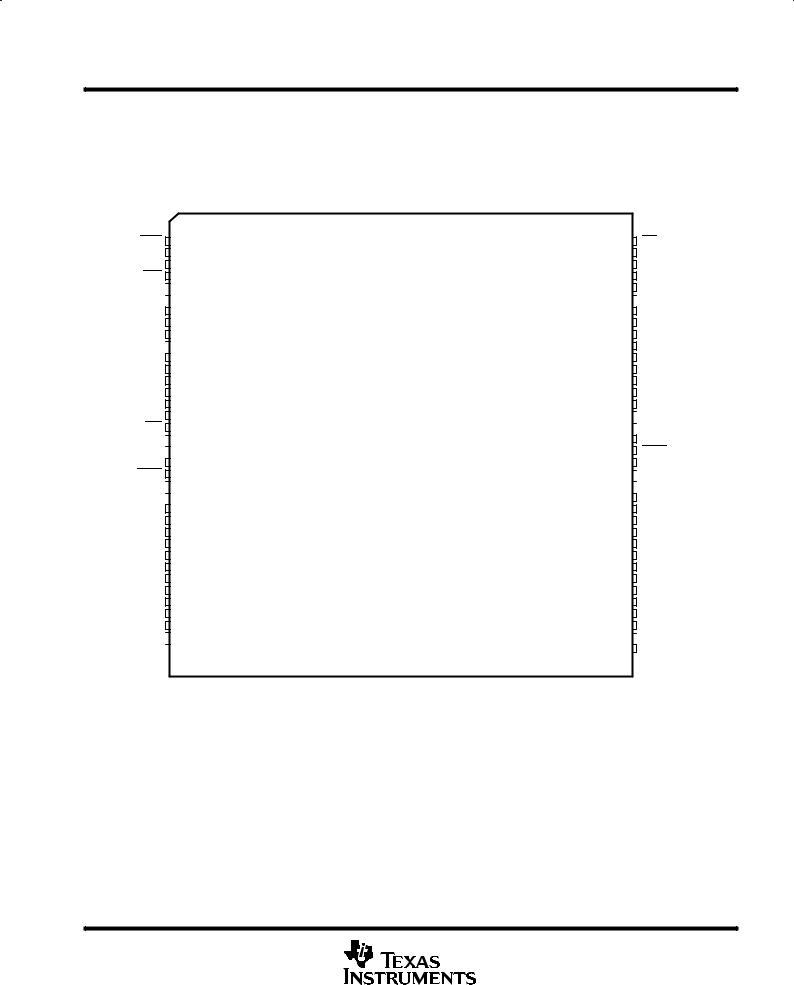
TMS320C5x, TMS320LC5x
DIGITAL SIGNAL PROCESSORS
SPRS030A ± APRIL 1995 ± REVISED APRIL 1996
TMS320C57S, TMS320LC57S
PGE PACKAGE
( TOP VIEW )
V |
|
V |
|
V |
|
NC CLKOUT1 XF |
|
HOLDA BDX DX HD7 |
|
BFSX HD6 |
|
FSX HD5 CLKMD2 |
HD4 V |
V |
|
TDO NC V |
|
X1 X2/CLKIN CLKMD3 NC BR HD3 NC STRB R/W PS |
IS DS |
|
|
HD2 |
V |
V |
|||||||||||||||||||||||||||||||||||||||||||||||||||||||||||||||||||||||||||||||||||||||||||||||||||||||||||||||||
|
|
|
|
|
|
|
|||||||||||||||||||||||||||||||||||||||||||||||||||||||||||||||||||||||||||||||||||||||||||||||||||||||||||||||||||||||||||||||||||
|
DDC |
|
DDI |
|
DDI |
|
|
|
|
|
|
|
|
|
|
|
|
|
|
|
|
|
|
|
|
|
|
|
|
|
|
|
|
|
|
|
|
|
|
|
|
|
|
|
|
|
|
|
|
|
|
|
|
|
|
|
|
|
|
SSI |
|
SSI |
|
|
|
|
|
|
|
|
|
DDC |
|
|
|
|
|
|
|
|
|
|
|
|
|
|
|
|
|
|
|
|
|
|
|
|
|
|
|
|
|
|
|
|
|
|
|
|
|
|
|
|
|
|
|
|
|
|
|
SSC |
|
SSC |
|||||||||||||||
|
|
|
|
|
|
|
|
|
|
|
|
|
|
|
|
|
|
|
|
|
|
|
|
|
|
|
|
|
|
|
|
|
|
|
|
|
|
|
|
|
|
|
|
|
|
|
|
|
|
|
|
|
|
|
|
|
|
|
|
|
|
|
|
|
|
|
|
|
|
|
|
|
|
|
|
|
|
|
|
|
|
|
|
|
|
|
|
|
|
|
|
|
|
|
|
|
|
|
|
|
|
|
|||||||||||||||||||||||||||||||||||
|
|
|
|
|
|
|
|
|
|
|
|
|
|
|
|
|
|
|
|
|
|
|
|
|
|
|
|
|
|
|
|
|
|
|
|
|
|
|
|
|
|
|
|
|
|
|
|
|
|
|
|
|
|
|
|
|
|
|
|
|
|
|
|
|
|
|
|
|
|
|
|
|
|
|
|
|
|
|
|
|
|
|
|
|
|
|
|
|
|
|
|
|
|
|
|||||||||||||||||||||||||||||||||||||||||||
|
|
|
|
|
|
|
|
|
|
|
|
|
|
|
|
|
|
|
|
|
|
|
|
|
|
|
|
|
|
|
|
|
|
|
|
|
|
|
|
|
|
|
|
|
|
|
|
|
|
|
|
|
|
|
|
|
|
|
|
|
|
|
|
|
|
|
|
|
|
|
|
|
|
|
|
|
|
|
|
|
|
|
|
|
|
|
|
|
|
|
|
|
|
|
|
|
|
|
|
|
|
|
|
|
|
|
|
|
|
|
|
|
|
|
|
|
|
|
|
|
|
|
|
|
|
|
|
|
|
|
|
|
|
|
|
|
|
|
|
|
|
|
|
|
|
|
|
|
|
|
|
|
|
|
|
|
|
|
|
|
|
|
|
|
|
|
|
|
|
|
|
|
|
|
|
|
|
|
|
|
|
|
|
|
|
|
|
|
|
|
|
|
|
|
|
|
|
|
|
|
|
|
|
|
|
|
|
|
|
|
|
|
|
|
|
|
|
|
|
|
|
|
|
|
|
|
|
|
|
|
|
|
|
|
|
|
|
|
|
|
|
|
|
|
|
|
|
|
|
|
|
|
|
|
|
|
|
|
|
|
|
|
|
|
|
|
|
|
|
|
|
|
|
|
|
HINT
EMU0
NC
EMU1/OFF VSSC 
VSSC 
TOUT
BCLKX
CLKX
VDDC 
BFSR
BCLKR
RS
READY
HOLD
NC
BIO
VDDC 
VDDC 
IAQ
TRST
VSSI 
VSSI 
MP/MC
D15
D14
D13
NC
D12
D11
D10
D9
NC
D8
VDDD 
VDDD 
1 
2
3
4
5
6
7
8
9
10
11
12
13
14
15
16
17
18
19
20
21
22
23
24
25
26
27
28
29
30
31
32
33
34
35
36
144 |
143 |
142 |
141 |
140 |
139 |
138 |
137 |
136 |
135 |
134 |
133 |
132 |
131 |
130 |
129 |
128 |
127 |
126 |
125 |
124 |
123 |
122 |
121 |
120 |
119 |
118 |
117 |
116 |
115 |
114 |
113 |
112 |
111 |
110 |
109 |
37 |
|
38 |
|
39 |
40 |
41 |
42 |
43 |
|
44 |
45 |
46 |
47 |
48 |
49 |
50 |
51 |
52 |
|
53 |
|
54 |
55 |
|
56 |
|
57 |
58 |
|
59 |
|
60 |
|
61 |
|
62 |
|
63 |
64 |
|
65 |
66 |
67 |
68 |
69 |
|
70 |
|
71 |
|
72 |
|
||||||||||||||||||||
|
|
|
|
|
|
|
|
|
|
|
|
|
|
|
|
|
|
|
|
|
|
|
|
|
|
|
|
|
|
|
|
|
|
|
|
|
|
|
|
|
|
|
|
|
|
|
|
|
|
|
|
|
|
|
|
|
|
|
|
|
|
|
|
|
|
|
|
|
|
|
|
|
|
|
|
|
|
|
|
|
|
|
|
|
|
|
|
|
|
|
|
|
|
|
|
|
|
|
|
|
|
|
|
|
|
|
|
|
|
|
|
|
|
|
|
|
|
|
|
|
|
|
|
|
|
|
|
|
|
|
|
|
|
|
|
|
|
|
|
|
|
|
|
|
|
V |
V |
D7 |
|
D6 |
|
NC |
|
D5 |
|
D4 |
D3 |
|
NC |
|
D2 |
D1 |
|
D0 |
|
HCNTL0 |
|
TMS |
|
HCNTL1 |
|
V |
V |
TCK |
|
V |
V |
NC |
|
HR/W |
INT1 |
INT2 |
INT3 |
INT4 |
HBIL |
|
NMI |
DR |
|
BDR |
|
FSR |
|
CLKR |
|
V |
V |
HAS |
NC |
|||||||||||||||||||
|
SSD |
SSD |
|
|
|
|
|
|
|
|
|
|
|
|
|
|
|
|
|
|
|
|
|
|
|
|
|
|
DDD |
DDD |
|
|
SSD |
SSD |
|
|
|
|
|
|
|
|
|
|
|
|
|
|
|
|
|
|
|
|
|
|
|
|
DDA |
DDA |
|
|
|
|
||||||||
|
|
|
|
|
|
|
|
|
|
|
|
|
|
|
|
|
|
|
|
|
|
|
|
|
|
|
|
|
|
|
|
|
|
|
|
|
|
|
|
|
|
|
|
|
|
|
|
|
|
|
|
|
|
|
|
|
|
|
|
|
|
|
|
|
||||||||
NOTE: NC = No connect (These pins are reserved.)
108 WE
107 HD1
106 RD
105 HD0
104 HRDY
103  VDDA
VDDA
102 A15
101 NC
100 A14
99 A13
98 A12
97 NC
96 A11
95 A10
94 CLKMD1
93  VSSA
VSSA
92  VSSA
VSSA
91 TDI
90 HDS1
89 HDS2
88  VDDI
VDDI
87  VDDI
VDDI
86 A9
85 A8
84 A7
83 NC
82 A6
81 A5
80 A4
79 A3
78 NC
77 A2
76 A1
75 A0
74  VSSA
VSSA
73 HCS
ADVANCE INFORMATION
POST OFFICE BOX 1443 •HOUSTON, TEXAS 77251±1443 |
15 |

TMS320C5x, TMS320LC5x
DIGITAL SIGNAL PROCESSORS
SPRS030A ± APRIL 1995 ± REVISED APRIL 1996
Pin Functions for the TMS320C57S, TMS320LC57S in the PGE Package
|
|
|
|
|
|
|
|
|
|
|
|
|
|
|
|
|
|
SIGNAL |
|
TYPE |
DESCRIPTION |
|
|||||||||
|
|
|
|
|
|
|
|
|
|
|
|
|
|
|
|
|
|
|
|
|
|
|
|
|
|
|
|
|
|
|
|
|
|
|
|
|
|
|
|
|
|
|
|
|
|
|
|
|
|
|
|
|
|
|
|
|
|
|
|
|
|
PARALLEL INTERFACE BUS |
|
|
|
|
|
|
|
|
|
|
|
|
|
|
|
|
|
|
|
|
|
|
|
|
|
|
|
|
|
|
|
|
|
|
A0 ± A15 |
|
I / O / Z |
16-bit external address bus (MSB: A15, LSB: A0) |
|
||||||||||||||||||||||||||
|
|
|
|
|
|
|
|
|
|
|
|
|
|
|
|
|
|
|
|
|
|
|
|
|
|
|
|
|
|
|
|
|
D0 ± D15 |
|
I / O / Z |
16-bit external data bus (MSB: D15, LSB: D0) |
|
||||||||||||||||||||||||||
|
|
|
|
|
|
|
|
|
|
|
|
|
|
|
|
|
|
|
|
|
|
|
|
|
|
|
|
|
|
|
|
|
|
|
|
|
|
|
|
|
|
|
|
|
|
|
|
|
|
|
|
|
|
|
|
|
|
|
|
|
O / Z |
Program, data, and I /O space select outputs, respectively |
|
|
PS, |
|
|
|
|
|
|
DS, |
|
|
|
IS |
|
|
|
|
|||||||||||||||
|
|
|
|
|
|
|
|
|
|
|
|
|
|
|
|
|
|
|
|
|
|
|
|
|
|
|
|
|
|||
|
|
|
|
|
|
|
|
|
|
|
|
|
|
|
|
|
|
|
|
|
|
|
|
|
|
|
|
|
I / O / Z |
Timing strobe for external cycles and external DMA |
|
|
STRB |
|
|
|
|
|
|
|
|
|
|
|
|||||||||||||||||||
|
|
|
|
|
|
|
|
|
|
|
|
|
|
|
|
|
|
|
|
|
|
|
|
|
|
|
|||||
|
R / |
|
|
|
|
|
|
|
|
|
|
|
|
|
|
|
|
|
|
|
|
|
|
|
|
|
|
|
I / O / Z |
Read/ write select for external cycles and external DMA |
|
|
W |
|
|
|
|
|
|
|
|
|
|
|
|
|
|||||||||||||||||
|
|
|
|
|
|
|
|
|
|
|
|
|
|
|
|
|
|
|
|
|
|
|
|
|
|
||||||
|
|
|
|
|
|
|
|
|
|
|
|
|
|
|
|
|
|
|
|
|
|
|
|
|
|
|
|
|
O / Z |
Read and write strobes, respectively, for external cycles |
|
|
RD, |
|
|
|
|
|
|
WE |
|
|
|
|
|
||||||||||||||||||
|
|
|
|
|
|
|
|
|
|
|
|
|
|
|
|
|
|
|
|
|
|
|
|
|
|||||||
|
READY |
|
|
|
|
I |
External bus ready/ wait-state control input |
|
|||||||||||||||||||||||
|
|
|
|
|
|
|
|
|
|
|
|
|
|
|
|
|
|
|
|
|
|
|
|
||||||||
|
|
|
|
|
|
|
|
|
|
|
|
|
|
|
|
|
|
|
|
|
|
|
|
|
|
|
|
|
I / O / Z |
Bus request. Arbitrates global memory and external DMA |
|
|
BR |
|
|
|
|
|
|
|
|
|
|
|
|
|
|
|
|
|
|
|
|
|
|||||||||
|
|
|
|
|
|
|
|
|
|
|
|
|
|
|
|
|
|
|
|
|
|
|
|
|
|
|
|
|
|
|
|
|
|
|
|
|
|
|
|
|
|
|
|
|
|
|
|
|
|
|
|
|
|
|
|
|
|
|
|
|
|
SYSTEM INTERFACE / CONTROL SIGNALS |
|
|
|
|
|
|
|
|
|
|
|
|
|
|
|
|
|
|
|
|
|
|
|
|
|
||||||||
|
RS |
|
|
|
|
|
|
|
|
|
|
|
|
|
|
|
|
|
|
|
|
I |
Reset. Initializes device and sets PC to zero |
|
|||||||
|
|
|
|
|
|
|
|
|
|
|
|
|
|
|
|
|
|
|
|
|
|
||||||||||
|
|
|
|
|
|
|
|
|
|
|
|
|
|
|
|
|
|
|
|
|
|
|
|
|
|
|
|
|
I |
Microprocessor/microcomputer mode select. Enables internal ROM |
|
|
MP/MC |
|
|
|
|
|
|
||||||||||||||||||||||||
|
|
|
|
|
|
|
|
|
|
|
|
|
|
|
|
|
|
|
|
|
|||||||||||
|
|
|
|
|
|
|
|
|
|
|
|
|
|
|
|
|
|
|
|
|
|
|
|
|
|
|
|
|
I |
Puts parallel I/ F bus in high-impedance state after current cycle |
|
|
HOLD |
|
|
|
|
|
|
|
|
|
|||||||||||||||||||||
|
|
|
|
|
|
|
|
|
|
|
|
|
|
|
|
|
|
|
|
||||||||||||
|
|
|
|
|
|
|
|
|
|
|
|
|
|
|
|
|
|
|
|
|
|
|
|
|
|
|
|
|
O / Z |
Hold acknowledge. Indicates external bus in hold state |
|
|
HOLDA |
|
|
|
|
|
|
||||||||||||||||||||||||
|
|
|
|
|
|
|
|
|
|
|
|
|
|
|
|
|
|
|
|
||||||||||||
|
XF |
|
|
|
|
O / Z |
External flag output. Set /cleared through software |
|
|||||||||||||||||||||||
|
|
|
|
|
|
|
|
|
|
|
|
|
|
|
|
|
|
|
|||||||||||||
|
|
|
|
|
|
|
|
|
|
|
|
|
|
|
|
|
|
|
|
|
|
|
|
|
|
|
|
|
I |
I /O branch input. Implements conditional branches |
|
|
BIO |
|
|
|
|
|
|
|
|
|
|
|
|
|
|
|
|
||||||||||||||
|
|
|
|
|
|
|
|
|
|
|
|
|
|
|
|
|
|
|
|||||||||||||
|
TOUT |
|
|
|
|
O / Z |
Timer output signal. Indicates output of internal timer |
|
|||||||||||||||||||||||
|
|
|
|
|
|
|
|
|
|
|
|
|
|
|
|
|
|
||||||||||||||
|
|
|
|
|
|
|
|
|
|
|
|
|
|
|
|
|
|
|
|
|
|
|
|
|
|
|
|
|
O / Z |
Instruction acquisition signal |
|
|
IAQ |
|
|
|
|
|
|
|
|
|
|
|
|
|
|
|
|||||||||||||||
|
|
|
|
|
|
|
|
|
|
|
|
|
|
± |
|
|
|
|
|
|
|
|
|
I |
External interrupt inputs |
|
|||||
|
INT1 |
|
INT4 |
|
|
|
|||||||||||||||||||||||||
|
|
|
|
|
|
|
|
|
|
|
|
|
|
|
|||||||||||||||||
|
|
|
|
|
|
|
|
|
|
|
|
|
|
|
|
|
|
|
|
|
|
|
|
|
|
|
|
|
I |
Nonmaskable external interrupt |
|
|
NMI |
|
|
|
|
|
|
|
|
|
|
|
|
||||||||||||||||||
|
|
|
|
|
|
|
|
|
|
|
|
|
|
|
|
|
|
|
|
|
|
|
|
|
|
|
|
|
|
|
|
|
|
|
|
|
|
|
|
|
|
|
|
|
|
|
|
|
|
|
|
|
|
|
|
|
|
|
|
|
|
SERIAL PORT INTERFACE (SPI) |
|
|
|
|
|
|
|
|
|
|
|
|
|
|
|
|
|||||||||||||||||
|
DR |
|
|
|
|
I |
Serial receive-data input |
|
|||||||||||||||||||||||
|
|
|
|
|
|
|
|
|
|
|
|
|
|
|
|||||||||||||||||
|
DX |
|
|
|
|
O / Z |
Serial transmit-data output. In high-impedance state when not transmitting |
|
|||||||||||||||||||||||
|
|
|
|
|
|
|
|
|
|
|
|
|
|
|
|||||||||||||||||
|
CLKR |
|
|
|
|
I |
Serial receive-data clock input |
|
|||||||||||||||||||||||
|
|
|
|
|
|
|
|
|
|
|
|
|
|
|
|||||||||||||||||
|
CLKX |
|
|
|
|
I / O / Z |
Serial transmit-data clock. Internal or external source |
|
|||||||||||||||||||||||
|
|
|
|
|
|
|
|
|
|
|
|
|
|
|
|||||||||||||||||
|
FSR |
|
|
|
|
I |
Serial receive-frame-synchronization input |
|
|||||||||||||||||||||||
|
|
|
|
|
|
|
|
|
|
|
|
|
|
|
|||||||||||||||||
|
FSX |
|
|
|
|
I / O / Z |
Serial transmit-frame-synchronization signal. Internal or external source |
|
|||||||||||||||||||||||
|
|
|
|
|
|
|
|
|
|
|
|
|
|
|
|
|
|
|
|
|
|
|
|
|
|
|
|
|
|
|
|
|
|
|
|
|
|
|
|
|
|
|
|
|
|
|
|
|
|
|
|
|
|
|
|
|
|
|
|
|
|
HOST PORT INTERFACE (HPI) |
|
|
|
|
|
|
|
|
|
|
|
|
|||||||||||||||||||||
|
HCNTL0 |
|
I |
HPI mode control 1 |
|
||||||||||||||||||||||||||
|
|
|
|
|
|
|
|
|
|
|
|
||||||||||||||||||||
|
HCNTL1 |
|
I |
HPI mode control 2 |
|
||||||||||||||||||||||||||
|
|
|
|
|
|
|
|
|
|
|
|
|
|
||||||||||||||||||
|
|
|
|
|
|
|
|
|
|
|
|
|
|
|
|
|
|
|
|
|
|
|
|
|
|
|
|
|
O / Z |
Host interrupt |
|
|
HINT |
|
|
|
|
|
|
|
|
||||||||||||||||||||||
|
|
|
|
|
|
|
|
|
|
|
|
|
|||||||||||||||||||
|
|
|
|
|
|
|
|
|
|
|
|
|
|
|
|
|
|
|
|
|
|
|
|
|
|
|
|
|
I |
HPI data strobe 1 |
|
|
HDS1 |
|
|
|
|
|
|
|
|||||||||||||||||||||||
|
|
|
|
|
|
|
|
|
|
|
|
|
|||||||||||||||||||
|
|
|
|
|
|
|
|
|
|
|
|
|
|
|
|
|
|
|
|
|
|
|
|
|
|
|
|
|
I |
HPI data strobe 2 |
|
|
HDS2 |
|
|
|
|
|
|
|
|||||||||||||||||||||||
|
|
|
|
|
|
|
|
|
|
|
|||||||||||||||||||||
|
HR / |
|
|
|
|
|
|
|
|
|
|
|
|
|
|
|
|
|
|
|
I |
HPI read / write strobe |
|
||||||||
|
W |
|
|
|
|
|
|
||||||||||||||||||||||||
|
|
|
|
|
|
|
|
|
|
||||||||||||||||||||||
|
|
|
|
|
|
|
|
|
|
|
|
|
|
|
|
|
|
|
|
|
|
|
|
|
|
|
|
|
I |
HPI address strobe |
|
|
HAS |
|
|
|
|
|
|
|
|||||||||||||||||||||||
|
|
|
|
|
|
|
|
|
|
||||||||||||||||||||||
|
HRDY |
|
|
|
|
O / Z |
HPI ready signal |
|
|||||||||||||||||||||||
|
|
|
|
|
|
|
|
|
|||||||||||||||||||||||
|
|
|
|
|
|
|
|
|
|
|
|
|
|
|
|
|
|
|
|
|
|
|
|
|
|
|
|
|
I |
HPI chip select |
|
|
HCS |
|
|
|
|
|
|
||||||||||||||||||||||||
|
|
|
|
|
|
|
|
|
|||||||||||||||||||||||
|
HBIL |
|
|
|
|
I |
HPI byte identification input |
|
|||||||||||||||||||||||
|
|
|
|
|
|
||||||||||||||||||||||||||
|
HD0 ± HD7 |
|
I / O / Z |
HPI data bus |
|
||||||||||||||||||||||||||
LEGEND: |
|
|
|
||||||||||||||||||||||||||||
|
I = |
Input |
|
|
|
||||||||||||||||||||||||||
|
O = |
Output |
|
|
|
||||||||||||||||||||||||||
|
Z = |
High impedance |
|
|
|
||||||||||||||||||||||||||
|
|
|
|
|
|
|
|
|
|
|
|
|
|
|
|
|
|
|
|
|
|
|
|
|
|
|
|
|
|
|
|
|
|
|
|
|
|
|
|
|
|
|
|
|
|
|
|
|
|
|
|
|
|
|
|
|
|
|
|
|
|
|
|
16 |
POST OFFICE BOX 1443 •HOUSTON, TEXAS 77251±1443 |

TMS320C5x, TMS320LC5x
DIGITAL SIGNAL PROCESSORS
SPRS030A ± APRIL 1995 ± REVISED APRIL 1996
Pin Functions for the TMS320C57S, TMS320LC57S in the PGE Package (Continued)
|
|
SIGNAL |
|
TYPE |
DESCRIPTION |
|||
|
|
|
|
|
|
|
|
|
|
|
|
|
|
|
|
|
BUFFERED SERIAL PORT |
|
|
|
|
|
|
|
|
|
|
BDR |
|
|
|
I |
BSP receive data input |
||
|
|
|
|
|
|
|
|
|
|
BDX |
|
|
|
O / Z |
BSP transmit data output; in high-impedance state when not transmitting |
||
|
|
|
|
|
|
|
|
|
|
BCLKR |
|
|
|
I |
BSP receive-data clock input |
||
|
|
|
|
|
|
|
|
|
|
BCLKX |
|
|
|
I / O / Z |
BSP transmit-data clock; internal or external source |
||
|
|
|
|
|
|
|
|
|
|
BFSR |
|
|
|
I |
BSP receive frame-synchronization input |
||
|
|
|
|
|
|
|
|
|
|
BFSX |
|
|
|
I / O / Z |
BSP transmit frame-synchronization signal; internal or external source |
||
|
|
|
|
|
|
|
|
|
|
|
|
|
|
|
|
|
EMULATION/JTAG INTERFACE |
|
|
|
|
|
|
|
|
|
|
TDI |
|
|
|
I |
JTAG-test-port scan data input |
||
|
|
|
|
|
|
|
|
|
|
TDO |
|
|
|
O / Z |
JTAG-test-port scan data output |
||
|
|
|
|
|
|
|
|
|
|
TMS |
|
|
|
I |
JTAG-test-port mode select input |
||
|
|
|
|
|
|
|
|
|
|
TCK |
|
|
|
I |
JTAG-port clock input |
||
|
|
|
|
|
|
|
|
|
|
|
|
|
|
|
|
I |
JTAG-port reset (with pulldown resistor). Disables JTAG when low |
|
TRST |
|
|
|
|
|
||
|
|
|
|
|
|
|
|
|
|
EMU0 |
|
|
|
I / O / Z |
Emulation control 0. Reserved for emulation use |
||
|
|
|
|
|
||||
|
EMU1/ |
|
|
|
|
I / O / Z |
Emulation control 1. Puts outputs in high-impedance state when low |
|
|
OFF |
|
|
|||||
|
|
|
|
|
|
|
|
|
|
|
|
|
|
|
|
|
CLOCK GENERATION AND CONTROL |
|
|
|
|
|
|
|
||
|
X1 |
|
|
|
O |
Oscillator output |
||
|
|
|
|
|
||||
|
X2 / CLKIN |
|
I |
PLL clock input |
||||
|
|
|
|
|
||||
|
CLKMD1, CLKMD2, |
|
I |
Clock-mode select inputs |
||||
|
CLKMD3 |
|
||||||
|
|
|
|
|||||
|
|
|
|
|
||||
|
CLKOUT1 |
|
O / Z |
Device system-clock output |
||||
|
|
|
|
|
|
|
|
|
|
|
|
|
|
|
|
|
POWER SUPPLY CONNECTIONS |
|
|
|
|
|
|
|
||
|
VDDA |
|
|
|
S |
Supply connection, address-bus output |
||
|
VDDD |
|
|
|
S |
Supply connection, data-bus output |
||
|
VDDC |
|
|
|
S |
Supply connection, control output |
||
|
VDDI |
|
|
|
S |
Supply connection, internal logic |
||
|
VSSA |
|
|
|
S |
Supply connection, address-bus output |
||
|
VSSD |
|
|
|
S |
Supply connection, data-bus output |
||
|
VSSC |
|
|
|
S |
Supply connection, control output |
||
|
VSSI |
|
|
|
S |
Supply connection, internal logic |
||
LEGEND: |
|
|
||||||
|
I = |
Input |
|
|
||||
|
O = |
Output |
|
|
||||
|
S = |
Supply |
|
|
||||
|
Z = |
High impedance |
|
|
||||
POST OFFICE BOX 1443 •HOUSTON, TEXAS 77251±1443 |
17 |

TMS320C5x, TMS320LC5x
DIGITAL SIGNAL PROCESSORS
SPRS030A ± APRIL 1995 ± REVISED APRIL 1996
architecture
The 'C5x's advanced Harvard-type architecture maximizes the processing power by maintaining two separate memory bus structures, program and data, for full-speed execution. Instructions support data transfers between the two spaces. This architecture permits coefficients stored in program memory to be read into the RAM, eliminating the need for a separate coefficient ROM. The 'C5x architecture also makes available immediate instructions and subroutines based on computed values. Increased throughput on the 'C5x for many DSP applications is accomplished using single-cycle multiply/accumulate instructions with a data-move option, up to eight auxiliary registers with a dedicated arithmetic unit, a parallel logic unit, and faster I/O necessary for data-intensive signal processing. The architectural design emphasizes overall speed, communication, and flexibility in processor configuration. Control signals and instructions provide floating-point support, block-memory transfers, communication to slower off-chip devices, and multiprocessing implementations as shown in the functional block diagram.
Table 3 explains the symbols that are used in the functional block diagram.
Table 3. Symbols Used in Functional Block Diagram
|
SYMBOL |
DESCRIPTION |
SYMBOL |
DESCRIPTION |
|
|
|
|
|
|
|
|
ABU |
Auto-buffering unit |
IFR |
Interrupt-flag register |
|
|
|
|
|
|
|
|
ACCB |
Accumulator buffer |
IMR |
Interrupt-mask register |
|
|
|
|
|
|
|
|
ACCH |
Accumulator high |
INDX |
Indirect-addressing-index register |
|
|
|
|
|
|
|
|
ACCL |
Accumulator low |
IR |
Instruction register |
|
|
|
|
|
|
|
|
ALU |
Arithmetic logic unit |
MCS |
Microcall stack |
|
|
|
|
|
|
|
|
ARAU |
Auxiliary-register arithmetic unit |
MUX |
Multiplexer |
|
|
|
|
|
|
|
|
ARB |
Auxiliary-register pointer buffer |
PAER |
Block-repeat-address end register |
|
|
|
|
|
|
|
|
ARCR |
Auxiliary-register compare register |
PASR |
Block-repeat-address start register |
|
|
|
|
|
|
|
|
ARP |
Auxiliary-register pointer |
PC |
Program counter |
|
|
|
|
|
|
|
|
ARR |
Address-receive register (ABU) |
PFC |
Prefetch counter |
|
|
|
|
|
|
|
|
AR0±AR7 |
Auxiliary registers |
PLU |
Parallel logic unit |
|
|
|
|
|
|
|
|
AXR |
Address-transmit register (ABU) |
PMST |
Processor-mode-status register |
|
|
|
|
|
|
|
|
BKR |
Receive-buffer-size register (ABU) |
PRD |
Timer-period register |
|
|
|
|
|
|
|
|
BKX |
Transmit-buffer-size register (ABU) |
PREG |
Product register |
|
|
|
|
|
|
|
|
BMAR |
Block-move-address register |
RPTC |
Repeat-counter register |
|
|
|
|
|
|
|
|
BRCR |
Block-repeat-counter register |
SARAM |
Single-access RAM |
|
|
|
|
|
|
|
|
BSP |
Buffered serial port |
SFL |
Left shifter |
|
|
|
|
|
|
|
|
C |
Carry bit |
SFR |
Right shifter |
|
|
|
|
|
|
|
|
CBER1 |
Circular buffer 1 end address |
SPC |
Serial-port interface-control register |
|
|
|
|
|
|
|
|
CBER2 |
Circular buffer 2 end address |
ST0,ST1 |
Status registers |
|
|
|
|
|
|
|
|
CBSR1 |
Circular buffer 1 start address |
TCSR |
TDM channel-select register |
|
|
|
|
|
|
|
|
CBSR2 |
Circular buffer 2 start address |
TCR |
Timer-control register |
|
|
|
|
|
|
|
|
DARAM |
Dual-access RAM |
TDM |
Time-division-multiplexed serial port |
|
|
|
|
|
|
|
|
DBMR |
Dynamic bit manipulation register |
TDXR |
TDM data transmit register |
|
|
|
|
|
|
|
|
DP |
Data memory page pointer |
TIM |
Timer-count register |
|
|
|
|
|
|
|
|
DRR |
Serial-port data receive register |
TRAD |
TDM received-address register |
|
|
|
|
|
|
|
|
DXR |
Serial-port data transmit register |
TRCV |
TDM data-receive register |
|
|
|
|
|
|
|
|
GREG |
Global memory allocation register |
TREG0 |
Temporary register for multiplication |
|
|
|
|
|
|
|
|
HPI |
Host port interface |
TREG1 |
Temporary register for dynamic shift count |
|
|
|
|
|
|
|
|
HPIAH |
HPI-address register (high bytes) |
TREG2 |
Temporary register used as bit pointer in dynamic-bit test |
|
|
|
|
|
|
|
|
HPIAL |
HPI-address register (low bytes) |
TRTA |
TDM receive-/transmit-address register |
|
|
|
|
|
|
|
|
HPICH |
HPI-control register (high bytes) |
TSPC |
TDM serial-port-control register |
|
|
|
|
|
|
|
|
HPICL |
HPI-control register (low bytes) |
|
|
|
|
|
|
|
|
|
|
|
|
|
|
|
|
|
|
|
|
|
18 |
POST OFFICE BOX 1443 •HOUSTON, TEXAS 77251±1443 |

TMS320C5x, TMS320LC5x
DIGITAL SIGNAL PROCESSORS
SPRS030A ± APRIL 1995 ± REVISED APRIL 1996
functional block diagram |
|
|
|
|
|
|
|
|
|
|
|
|
||||
CLKMD1 |
|
|
|
|
|
|
Program Bus |
|
|
|
|
|
|
|
|
|
|
|
|
|
|
|
|
|
|
|
|
|
|
|
|
Serial Port 1 |
|
CLKMD2 |
|
|
|
|
|
|
|
|
|
|
|
|
|
|
Bus |
|
|
|
|
|
|
|
|
|
|
|
|
|
|
|
|
||
IS |
|
|
|
|
16 |
|
|
|
|
|
|
|
|
|
Data |
SPC |
DS |
|
|
|
|
|
|
|
|
|
|
|
|
|
|||
PS |
|
|
|
|
|
|
|
|
|
|
|
|
|
|
|
DXR |
|
|
|
|
|
|
|
|
|
|
|
|
|
|
|
|
|
RW |
|
|
X1 |
|
PFC(16) |
16 |
|
|
|
|
|
|
|
|
|
|
|
|
|
|
|
|
|
|
|
|
|
|
|
|
DRR |
||
STRB |
|
|
CLKOUT1 |
|
|
|
|
PAER(16) |
|
|
|
|
|
|
||
|
|
|
|
|
|
|
16 |
|
|
|
|
|
||||
READY |
|
|
X2/CLKIN |
|
|
|
|
|
16 |
|
|
|
|
|
|
|
|
|
|
|
|
|
|
|
|
|
|
|
|
|
|||
BR |
|
|
CLKIN2/CLKMD3 |
|
|
|
|
|
|
|
|
|
² |
|
||
|
|
|
|
MUX |
|
|
|
|
|
|
|
Serial Port 2 |
||||
XF |
Control |
|
|
|
16 |
|
16 |
Compare |
|
|
|
|
||||
|
|
|
|
|
|
|
|
|
|
|||||||
|
16 |
|
|
|
16 |
|
|
|
|
|
||||||
HOLD |
|
|
|
16 |
16 |
|
16 |
|
|
|
|
|||||
|
|
|
|
|
|
|
|
|
|
|
|
SPC |
||||
HOLDA |
|
|
|
|
|
|
|
|
|
|
|
|
|
IR(16) |
|
|
|
|
|
|
|
|
|
|
|
|
|
|
|
|
|
||
IAQ |
|
|
|
MCS(16) |
|
|
PC(16) |
|
PASR(16) |
|
|
|
BMAR(16) |
|
DXR |
|
BO |
|
|
RD |
|
|
|
|
|
|
|
|
|
|
|
||
|
|
|
|
|
16 |
|
|
|
|
16 |
|
ST0(16) |
|
|
||
RS |
|
|
WE |
|
|
|
|
|
|
|
|
|
|
|||
|
|
|
|
|
|
|
|
|
|
|
|
DRR |
||||
|
|
|
|
|
|
|
|
|
|
|
|
|
|
|||
IACK |
|
|
NMI |
|
|
|
|
|
|
|
|
|
|
ST1(16) |
|
|
|
|
|
|
|
|
|
|
|
|
|
|
|
|
|||
MP/MC |
|
|
|
Address |
|
Stack |
|
16 |
|
|
|
|
PMST(16) |
² |
|
|
|
|
|
|
|
|
|
|
|
|
|
||||||
|
|
|
|
|
|
|
|
|
|
|
|
|
|
TDM |
||
INT(1±4) |
|
|
|
Program |
ROM |
|
(8x16) |
|
|
|
|
|
|
RPTC(16) |
||
4 |
|
|
|
|
|
|
|
|
|
|
|
|||||
|
|
|
'C50 |
2K |
|
|
|
|
|
|
|
|
|
|
|
|
|
|
|
|
|
|
|
|
|
|
|
|
IMR(16) |
|
TSPC |
||
|
|
|
|
'C51 |
8K |
|
|
|
|
|
|
|
|
|
||
|
|
|
|
|
|
|
|
|
|
|
|
IFR(16) |
|
|
||
|
|
|
|
'C52 |
4K |
|
|
|
|
|
|
|
|
|
TDXR |
|
|
|
|
|
|
|
|
|
|
|
|
|
|
|
|||
|
|
|
|
'C53 |
16K |
|
|
|
|
|
|
|
|
GREG(16) |
|
|
|
|
|
|
|
|
|
|
|
|
|
|
|
|
|||
A15±A0 |
|
MUX |
16 |
'C56 |
32K |
|
|
|
16 |
|
|
|
BRCR(16) |
|
TRCV |
|
|
|
'C57 |
32K |
|
|
|
|
|
|
|
||||||
16 |
|
|
|
|
|
|
|
|
|
TREG1(5) |
|
|
||||
|
|
|
|
|
|
|
|
|
|
|
|
|
|
TCSR(8) |
||
|
|
|
16 |
Instruction |
|
|
|
|
|
|
|
|
TREG2(4) |
|
||
|
|
|
|
|
|
|
|
|
|
|
|
|
|
|||
RBIT |
|
|
|
|
16 |
|
|
|
|
16 |
|
|
|
|
TRTA |
|
|
|
|
|
|
|
|
|
|
|
|
|
|
|
|
||
|
|
|
|
|
|
|
|
|
|
|
|
|
Program Bus |
|
TRAD(16) |
|
|
|
MUX |
|
|
|
|
|
|
|
|
|
|
|
|
|
|
D15±D0 |
|
|
|
|
|
|
|
|
|
|
|
|
|
² |
|
|
|
|
|
|
|
|
|
|
|
|
|
|
|
|
|
||
|
16 |
|
|
|
|
|
|
|
|
|
|
|
|
|
BSP |
|
|
|
|
|
16 |
|
|
|
|
|
|
Data Bus |
|
|
|
DXR |
|
|
|
|
|
|
|
|
|
|
|
|
|
|
|
|
|
|
Bus |
|
|
16 |
16 |
|
|
|
|
|
|
|
|
|
|
|
AXR(11) |
|
|
|
|
16 |
|
|
|
|
|
|
|
|
|
|
||
|
|
|
|
|
|
|
|
|
|
|
|
|
|
|
||
|
|
|
|
|
|
|
|
|
|
|
|
|
|
|
|
|
Data |
|
3 |
|
|
|
|
9 |
7 LSB |
|
16 |
16 |
16 |
16 |
16 |
|
BKX(11) |
|
|
|
|
|
|
|
from IR |
|
|
|||||||
|
|
|
|
AR0(16) |
|
|
|
|
|
|
|
|
|
|
|
|
|
|
|
|
AR1(16) |
DP(9) |
|
|
|
|
|
|
|
|
DRR |
||
|
|
|
|
|
|
|
MUX |
|
|
DBMR(16) |
|
|
||||
|
|
|
|
|
|
|
|
|
|
|
|
|
|
|
||
|
|
|
|
AR2(16) |
|
|
|
|
|
|
|
|
|
|
ARR(11) |
|
|
|
|
|
|
|
|
|
|
16 |
16 |
|
16 |
|
|
|
|
|
ARP(3) |
3 |
AR3(16) |
|
|
|
|
|
|
|
|
|||||
|
|
|
|
9 |
|
|
|
|
|
|
|
|
|
|||
|
|
|
|
|
|
|
|
|
|
|
|
|
|
BKR(11) |
||
|
|
|
|
AR4(16) |
|
|
|
|
|
|
|
|
|
|||
|
|
3 |
|
|
|
|
|
|
|
|
|
|
|
|||
|
|
|
|
|
|
|
|
|
|
|
16 |
|
|
|||
|
|
|
|
|
|
|
|
|
|
|
|
|
|
|
|
|
|
|
|
|
AR5(16) |
|
|
|
|
|
TREG0(16) |
|
|
MUX |
|
|
|
|
ARB(3) |
|
AR6(16) |
|
|
|
|
|
|
|
|
|
|
Timer |
||
|
|
|
|
AR7(16) |
|
|
|
|
|
Multiplier |
|
|
|
|
TCR |
|
|
|
|
|
|
|
|
|
|
|
|
|
|
|
|||
|
|
|
|
|
|
|
|
|
|
|
|
|
|
|
|
|
|
3 |
|
|
CBSR1(16) |
|
|
SFL(0±16) |
|
PREG(32) |
|
|
16 |
|
|
||
|
|
|
|
|
|
|
|
|
|
|
|
PRD |
||||
|
|
|
|
CBSR2(16) |
|
|
|
|
|
|
|
|||||
|
|
|
|
|
|
|
|
|
|
|
|
|
|
|||
|
|
|
|
|
16 |
|
|
|
|
|
|
|
|
|
||
|
|
|
|
CBER1(16) |
|
|
|
|
32 |
|
|
|
|
|
||
|
|
|
|
|
|
|
|
|
|
PLU (16) |
|
TIM |
||||
|
|
|
|
|
|
|
|
|
|
|
|
|||||
|
|
|
|
|
|
|
|
|
MUX |
|
|
|
|
|||
|
|
MUX |
|
CBER2(16) |
|
|
|
|
SFL (±6, 0, 1, 4) |
|
|
|
|
|
||
|
|
|
|
|
|
|
|
|
|
|
|
|
|
|
||
|
|
|
|
|
|
|
32 |
|
|
|
|
|
|
² |
|
|
|
|
|
|
INDX(16) |
|
|
|
32 |
32 |
|
|
|
HPI |
|||
|
|
|
|
ARCR(16) |
|
|
|
|
|
|
|
|
||||
|
|
|
|
|
|
|
|
|
|
|
|
|
|
|
||
|
|
|
|
|
16 |
|
SFR(0±16) |
|
|
|
|
|
|
|
HPICL |
|
|
|
|
|
|
|
|
|
|
|
|
|
|
|
|
||
|
|
|
|
|
|
|
|
|
|
|
MUX |
|
|
|
|
|
|
|
|
|
|
|
|
|
|
|
|
|
|
|
|
|
HPIAL |
|
|
|
|
ARAU(16) |
MUX |
|
|
|
|
32 |
|
|
|
|
HPICH |
|
|
|
|
|
|
|
|
|
|
|
|
|
|
|
|
||
|
|
|
|
|
|
|
|
|
|
|
|
|
|
|
|
|
|
|
|
|
|
|
|
|
32 |
|
ALU(32) |
|
32 |
16 |
|
HPIAH |
|
|
Data/Prog |
|
|
|
|
|
|
|
|
|
|
|
|
|||
|
|
|
|
|
|
|
|
|
|
|
|
|
|
|
||
|
SARAM |
|
MUX |
|
MUX |
|
|
|
|
32 |
|
|
|
|
|
|
|
|
|
|
|
|
|
|
|
|
|
|
|
|
|||
|
'C50 |
9K |
|
|
|
|
|
|
|
|
|
|
|
|
||
|
|
|
|
|
|
|
|
|
|
|
|
|
|
|
||
|
'C51 |
1K |
|
|
|
|
|
|
|
|
|
|
|
|
|
|
|
'C53 |
3K |
|
Data/Prog |
|
Data |
|
C |
ACCH(16) |
ACCL(16) |
ACCB(32) |
DataBus |
|
|||
|
'C56 |
6K |
|
DARAM |
|
DARAM |
|
|
|
32 |
|
|
ProgramBus |
|
||
|
'C57 |
6K |
|
B0 (512x16) |
|
B2 (32x16) |
|
|
|
|
|
|
||||
|
|
|
|
|
|
B1 (512x16) |
|
|
|
|
|
|
|
|
|
|
|
|
MUX |
|
MUX |
|
|
16 |
|
|
Shifter(0±7) |
|
|
|
|
|
|
|
|
|
|
|
|
|
|
|
|
|
|
|
|
|||
|
|
|
|
|
|
|
|
16 |
|
|
16 |
|
|
|
|
|
|
|
16 |
|
16 |
|
|
|
|
|
|
|
|
|
|
|
|
|
|
|
|
|
|
|
|
|
|
|
|
|
|
|
|
|
|
|
|
|
|
|
|
|
16 |
|
|
|
|
|
|
|
|
DX
CLKX
FSX
DR
FSR
CLKR
DX2
CLKX2
FSX2
DR2
FSR2
CLKR2
TDX
TFRM
TCLKX
TDR
TADD
TCLKR
BDX
DFSX
BCLKX
BDR
BFSR
BCLKR
TOUT
HD0
HD7
HCNTL1
HCNTL0 HBIL HCS HDS(1±1) HAS
HR/W
HRDY
HINT
² Not available on all devices (see Table 1).
NOTES: A. Signals in shaded text are not available on 100-pin QFP packages.
B. Symbol descriptions appear in Table 3.
POST OFFICE BOX 1443 •HOUSTON, TEXAS 77251±1443 |
19 |

TMS320C5x, TMS320LC5x
DIGITAL SIGNAL PROCESSORS
SPRS030A ± APRIL 1995 ± REVISED APRIL 1996
32-bit ALU/accumulator
The 32-bit ALU and accumulator implement a wide range of arithmetic and logical functions, the majority of which execute in a single cycle. The ALU is a general-purpose arithmetic/logic unit that operates on 16-bit words taken from data memory or derived from immediate instructions. In addition to the usual arithmetic instructions, the ALU can perform Boolean operations, facilitating the bit manipulation ability required of a high-speed controller. One input to the ALU always is supplied by the accumulator, and the other input can be furnished from the product register (PREG) of the multiplier, the accumulator buffer (ACCB), or the output of the scaling shifter [which has been read from data memory or from the accumulator (ACC)]. After the ALU performs the arithmetic or logical operation, the result is stored in the ACC where additional operations, such as shifting, can be performed. Data input to the ALU can be scaled by the scaling shifter. The 32-bit ACC is split into two 16-bit segments for storage in data memory. Shifters at the output of the ACC provide a left shift of 0 to 7 places. This shift is performed while the data is being transferred to the data bus for storage. The contents of the ACC remain unchanged. When the postscaling shifter is used on the high word of the ACC (bits 31±16), the most significant bits (MSBs) are lost and the least significant bits (LSBs) are filled with bits shifted in from the low word (bits 15±0). When the postscaling shifter is used on the low word, the LSBs are filled with zeros.
The 'C5x supports floating-point operations for applications requiring a large dynamic range. By performing left shifts, the normalization instruction (NORM) is used to normalize fixed-point numbers contained in the ACC. The four bits of the TREG1 define a variable shift through the scaling shifter for the ADDT/LACT/SUBT instructions (add to/load to/subtract from ACC with shift specified by TREG1). These instructions are useful in denormalizing a number (converting from floating point to fixed point). They are also useful for executing an automatic gain control (AGC) going into a filter.
The single-cycle 1-bit to 16-bit right shift of the ACC efficiently aligns the ACC's contents. This, coupled with the 32-bit temporary buffer on the ACC, enhances the effectiveness of the ALU in extended-precision arithmetic. The ACCB provides a temporary storage place for a fast save of the ACC. The ACCB also can be used as an input to the ALU. The minimum or maximum value in a string of numbers is found by comparing the contents of the ACCB with the contents of the ACC. The minimum or maximum value is placed in both registers, and, if the condition is met, the carry bit (C) is set to 1. The minimum and maximum functions are executed by the CRLT and CRGT instructions, respectively.
scaling shifters
The 'C5x provides a scaling shifter that has a 16-bit input connected to the data bus and a 32-bit output connected to the ALU. This scaling shifter produces a left shift of 0 to 16 bits on the input data. The shift count is specified by a constant embedded in the instruction word or by the value in TREG1. The LSBs of the output are filled with zeros; the MSBs may be either filled with zeros or sign extended, depending upon the value of the sign-extension mode (SXM) bit of status register ST1.
The 'C5x also contains several other shifters that allow it to perform numerical scaling, bit extraction, extended-precision arithmetic, and overflow prevention. These shifters are connected to the output of the product register and the ACC.
parallel logic unit
The parallel logic unit (PLU) is a second logic unit, additional to the main ALU, that executes logic operations on data without affecting the contents of the ACC. The PLU provides the bit-manipulation ability required of a high-speed controller and simplifies control/status register operations. The PLU provides a direct logic operation path to data memory space and can set, clear, test, or toggle multiple bits directly in a data memory location, a control/status register, or any register that is mapped into data memory space.
20 |
POST OFFICE BOX 1443 •HOUSTON, TEXAS 77251±1443 |
TMS320C5x, TMS320LC5x
DIGITAL SIGNAL PROCESSORS
SPRS030A ± APRIL 1995 ± REVISED APRIL 1996
16 × 16-bit parallel multiplier
The 'C5x uses a 16 × 16-bit hardware multiplier that is capable of computing a signed or an unsigned 32-bit product in a single machine cycle. All multiply instructions, except the MPYU (multiply unsigned) instruction, perform a signed multiply operation in the multiplier. That is, two numbers being multiplied are treated as 2s-complement numbers, and the result is a 32-bit 2s-complement number.
There are two registers associated with the multiplier: TREG0, a 16-bit temporary register that holds one of the operands for the multiplier, and PREG, the 32-bit product register that holds the product. Four product shift modes (PM) are available at the PREG's output. These shift modes are useful for performing multiply/accumulate operations, performing fractional arithmetic, or justifying fractional products. The PM field of status register ST1 specifies the PM shift mode.
The product can be shifted one bit to compensate for the extra sign bit gained in multiplying two 16-bit 2s-complement numbers (MPY). A 4-bit shift is used in conjunction with the MPY instruction with a short immediate value (13 bits or less) to eliminate the four extra sign bits gained in multiplying a 16-bit number by a 13-bit number. Finally, the output of PREG can, instead, be right-shifted 6 bits to enable the execution of up to 128 consecutive multiply/accumulates without the possibility of overflow.
The load-TREG0 (LT) instruction normally loads TREG0 to provide one operand (from the data bus), and the MPY instruction provides the second operand (also from the data bus). A multiplication also can be performed with a short or long immediate operand by using the MPY instruction with an immediate operand. A product is obtained every two cycles except when a long immediate operand is used.
Four multiply/accumulate instructions (MAC, MACD, MADD, and MADS as defined in Table 7) fully utilize the computational bandwidth of the multiplier, allowing both operands to be processed simultaneously. The data for these operations is transferred to the multiplier during each cycle through the program and data buses. This facilitates single-cycle multiply/accumulates when used with repeat (RPT and RPTZ) instructions. In these instructions, the coefficient addresses are generated by the PC, while the data addresses are generated by the ARAU. This allows the repeated instruction to access the values sequentially from the coefficient table and step through the data in any of the indirect addressing modes. The RPTZ instruction also clears the accumulator and the product register to initialize the multiply/accumulate operation.
The MACD and MADD instructions, when repeated, support filter constructs (weighted running averages) so that as the sum-of-products is executed, the sample data is shifted in memory to make room for the next sample and to eliminate the oldest sample. Circular addressing with MAC and MADS instructions also can be used to support filter implementation.
auxiliary registers and auxiliary-register arithmetic unit (ARAU)
The 'C5x provides a register file containing eight auxiliary registers (AR0±AR7). The auxiliary registers are used for indirect addressing of the data memory or for temporary data storage. Indirect auxiliary-register addressing allows placement of the data memory address of an instruction operand into one of the auxiliary registers. These registers are referenced with a 3-bit auxiliary register pointer (ARP) that is loaded with a value from 0 through 7, designated AR0 through AR7, respectively. The auxiliary registers and the ARP can be loaded from data memory, the ACC, the product register, or by an immediate operand defined in the instruction. The contents of these registers can be stored in data memory or used as inputs to the central arithmetic logic unit (CALU). These registers are accessible as memory-mapped locations within the 'C5x data-memory space.
The auxiliary register file (AR0±AR7) is connected to the auxiliary register arithmetic unit (ARAU). The ARAU can autoindex the current auxiliary register while the data memory location is being addressed. Indexing can be performed either by ±1 or by the contents of the INDX register. As a result, accessing tables of information does not require the CALU for address manipulation; thus, the CALU is free for other operations in parallel.
POST OFFICE BOX 1443 •HOUSTON, TEXAS 77251±1443 |
21 |

TMS320C5x, TMS320LC5x
DIGITAL SIGNAL PROCESSORS
SPRS030A ± APRIL 1995 ± REVISED APRIL 1996
memory
The 'C5x implements three separate address spaces for program memory, data memory, and I/O. Each space accommodates a total of 64K 16-bit words (see Figures 1 through 7). Within the 64K words of data space, the 256 to 32K words at the top of the address range can be defined to be external global memory in increments of powers of two, as specified by the contents of the global memory allocation register (GREG). Access to global memory is arbitrated using the global memory bus request (BR) signal.
The 'C5x devices include a considerable amount of on-chip memory to aid in system performance and integration including ROM, single-access RAM (SARAM), and dual-access RAM (DARAM). The amount and types of memory available on each device are shown in Table 1.
On the 'C5x, the first 96 (0±5Fh) data-memory locations are allocated for memory-mapped registers. This memory-mapped register space contains various control and status registers including those for the CPU, serial port, timer, and software wait-state generators. Additionally, the first 16 I/O port locations are mapped into this data-memory space, allowing them to be accessed either as data memory using single-word instructions or as I/O locations with two-word instructions. Two-word instructions allow access to the full 64K words of I/O space.
The mask-programmable ROM is located in program memory space. Customers can arrange to have this ROM programmed with contents unique to to any particular application. The ROM is enabled or disabled by the state of the MP/MC control input upon resetting the device or by manipulating the MP/MC bit in the PMST status register after reset. The ROM occupies the lowest block of program memory when enabled. When disabled, these addresses are located in the device's external program-memory space.
The 'C5x also has a mask-programmable option that provides security protection for the contents of on-chip ROM. When this internal option bit is programmed, no externally-originating instruction can access the on-chip ROM. This feature can be used to provide security for proprietary algorithms.
An optional boot loader is available in the device's on-chip ROM. This boot loader can be used to transfer a program automatically from data memory or the serial port to anywhere in program memory. In data memory, the program can be located on any 1K-word boundary and can be in either byte-wide or 16-bit word format. Once the code is transferred, the boot loader releases control to the program for execution.
The 'C5x devices provide two types of RAM: single-access RAM (SARAM) and dual-access RAM (DARAM). The single-access RAM requires a full machine cycle to perform a read or a write; however, this is not one large RAM block in which only one access per cycle is allowed. It is made up of 2K-word size-independent RAM blocks and each one allows one CPU access per cycle. The CPU can read or write one block while accessing another block at the same time. All 'C5x processors support multiple accesses to its SARAM in one cycle as long as they go to different RAM blocks. If the total SARAM size is not a multiple of two, one block is made smaller than 2K words. With an understanding of this structure, programmers can arrange code and data appropriately to improve code performance. Table 4 shows the sizes of available SARAM on the applicable 'C5x devices.
Table 4. SARAM Block Sizes
DEVICE |
NUMBER OF SARAM BLOCKS |
|
|
'C50 / 'LC50 |
Four 2K blocks and one 1K block |
|
|
'C51/ 'LC51 |
One 1K block |
|
|
'C53/ 'C53S / 'LC53 |
One 2K block and one 1K block |
|
|
'LC56 |
Three 2K blocks |
|
|
'C57S/ 'LC57/'LC57S |
Three 2K blocks |
memory (continued)
The 'C5x dual-access RAM (DARAM) allows writes to, and reads from, the RAM in the same cycle without the address restrictions of the SARAM. The dual-access RAM is configured in three blocks: block 0 (B0), block 1 (B1), and block 2 (B2). Block 1 is 512 words in data memory and block 2 is 32 words in data memory. Block 0
22 |
POST OFFICE BOX 1443 •HOUSTON, TEXAS 77251±1443 |

TMS320C5x, TMS320LC5x
DIGITAL SIGNAL PROCESSORS
SPRS030A ± APRIL 1995 ± REVISED APRIL 1996
is a 512-word block which can be configured as data or program memory. The CLRC CNF (configure B0 as data memory) and SETC CNF (configure B0 as program memory) instructions allow dynamic configuration of the memory maps through software. When using block 0 as program memory, instructions can be downloaded from external program memory into on-chip RAM and then executed.
When using on-chip RAM, ROM, or high-speed external memory, the 'C5x runs at full speed with no wait states. The ability of the DARAM to allow two accesses to be performed in one cycle, coupled with the parallel nature of the 'C5x architecture, enables the device to perform three concurrent memory accesses in any given machine cycle. Externally, the READY line can be used to interface the 'C5x to slower, less expensive external memory. Downloading programs from slow off-chip memory to on-chip RAM can speed processing while cutting system costs.
Hex |
|
Program |
Hex |
|
Program |
Hex |
Data |
||||||
0000 |
|
Interrupts and |
|
0000 |
|
Interrupts and |
|
0000 |
Memory-Mapped |
||||
|
|
Reserved |
|
|
|
Reserved |
|
005F |
Registers |
||||
|
|
(external) |
|
|
|
(on-chip) |
|
|
|||||
003F |
|
|
003F |
|
|
0060 |
On-Chip |
||||||
|
|
|
|
|
|
|
|
|
|
||||
0040 |
|
External |
|
0040 |
|
On-Chip |
|
007F |
DARAM B2 |
||||
|
|
|
|
|
|
|
|||||||
|
|
|
|
|
ROM |
|
|
||||||
07FF |
|
|
|
|
|
07FF |
|
|
0080 |
Reserved |
|||
|
|
|
|
|
|
|
|
|
|
||||
|
|
|
|
|
|
|
|
|
|
|
|||
0800 |
|
|
|
|
|
0800 |
|
|
|
|
|
00FF |
|
|
|
On-Chip SARAM |
|
|
|
On-Chip SARAM |
|
0100 |
On-Chip DARAM B0 |
||||
|
|
|
|
|
|
|
(CNF = 0) |
||||||
|
|
(RAM = 1) |
|
|
|
(RAM = 1) |
|
02FF |
Reserved (CNF = 1) |
||||
|
|
External |
|
|
|
External |
|
||||||
|
|
|
|
|
|
0300 |
On-Chip |
||||||
|
|
(RAM = 0) |
|
|
|
(RAM = 0) |
|
||||||
|
|
|
|
|
|
|
DARAM B1 |
||||||
|
|
|
|
|
|
|
|
|
|
|
|
04FF |
|
2BFF |
|
|
|
|
|
2BFF |
|
|
|
|
|
|
|
|
|
|
|
|
|
|
|
|
|
|
|||
|
|
|
|
|
|
|
|
|
|
0500 |
Reserved |
||
2C00 |
|
|
|
|
|
2C00 |
|
|
|
|
|
|
|
|
|
|
|
|
|
|
|
|
|
|
|
07FF |
|
|
|
|
|
|
|
|
|
|
|
|
|
|
|
|
|
External |
|
|
|
External |
|
0800 |
On-Chip SARAM |
||||
|
|
|
|
|
|
|
(OVLY = 1) |
||||||
|
|
|
|
|
|
|
|
|
|
|
|
|
|
|
|
|
|
|
|
|
|
|
|
|
|
2BFF |
External (OVLY = 0) |
FDFF |
|
|
|
|
|
FDFF |
|
|
|
|
|
|
|
|
|
|
|
|
|
|
|
|
|
2C00 |
|
||
FE00 |
|
On-Chip DARAM B0 |
|
FE00 |
|
On-Chip DARAM B0 |
|
|
External |
||||
|
|
(CNF = 1) |
|
|
|
(CNF = 1) |
|
|
|||||
|
|
|
|
|
|
|
|
||||||
FFFF |
|
External (CNF = 0) |
|
FFFF |
|
External (CNF = 0) |
|
FFFF |
|
||||
|
|
|
|
|
|
|
|
|
|
|
|||
|
|
MP/ |
MC |
= 1 |
|
|
|
MP/ |
MC |
= 0 |
|
|
|
|
(microprocessor mode) |
|
(microcomputer mode) |
|
|
||||||||
Figure 1. TMS320C50 and TMS320LC50 Memory Map
POST OFFICE BOX 1443 •HOUSTON, TEXAS 77251±1443 |
23 |

TMS320C5x, TMS320LC5x
DIGITAL SIGNAL PROCESSORS
SPRS030A ± APRIL 1995 ± REVISED APRIL 1996
Hex |
|
Program |
Hex |
|
Program |
Hex |
|
Data |
||||||||||||||||
0000 |
|
|
Interrupts and |
|
|
0000 |
|
|
Interrupts and |
|
|
0000 |
|
Memory-Mapped |
|
|||||||||
|
|
|
|
|
|
|
|
|
|
|
|
|
||||||||||||
|
|
|
Reserved |
|
|
|
|
|
Reserved |
|
|
005F |
|
|
Registers |
|
||||||||
003F |
|
|
(external) |
|
|
003F |
|
|
(on-chip) |
|
|
0060 |
|
|
On-Chip |
|
||||||||
|
|
|
|
|
|
|
|
|
|
|
|
|
|
|
|
|
|
|
|
|
||||
0040 |
|
|
External |
|
|
0040 |
|
|
On-Chip |
|
|
007F |
|
|
DARAM B2 |
|
||||||||
|
|
|
|
|
|
|
|
|
|
|
|
|
|
|||||||||||
|
|
|
|
|
|
|
|
ROM |
|
|
|
|
|
|
||||||||||
1FFF |
|
|
|
|
|
|
|
|
|
1FFF |
|
|
|
|
0080 |
|
|
Reserved |
|
|||||
|
|
|
|
|
|
|
|
|
|
|
|
|
|
|
|
|
|
|
|
|
||||
|
|
|
|
|
|
|
|
|
|
|
|
|
|
|
|
|
|
|
|
|
|
|||
2000 |
|
|
|
|
|
|
|
|
|
2000 |
|
|
|
|
|
|
|
|
|
00FF |
|
|
|
|
|
|
|
|
|
|
|
|
|
|
|
|
|
|
|
|
|
|
|
|
0100 |
|
On-Chip DARAM |
|
|
|
|
|
On-Chip SARAM |
|
|
|
|
On-Chip SARAM |
|
|
|
|
|
B0 (CNF = 0) |
|
|||||||||
|
|
|
(RAM = 1) |
|
|
|
|
|
(RAM = 1) |
|
|
02FF |
|
Reserved (CNF = 1) |
|
|||||||||
|
|
|
External |
|
|
|
|
|
External |
|
|
0300 |
|
|
On-Chip |
|
||||||||
|
|
|
(RAM = 0) |
|
|
|
|
|
(RAM = 0) |
|
|
|
|
|
|
|||||||||
|
|
|
|
|
|
|
|
|
|
|
|
|
DARAM B1 |
|
||||||||||
|
|
|
|
|
|
|
|
|
|
|
|
|
|
|
|
|
|
|
|
04FF |
|
|
|
|
23FF |
|
|
|
|
|
|
|
|
|
23FF |
|
|
|
|
|
|
|
|
|
|
|
|
|
|
|
|
|
|
|
|
|
|
|
|
|
|
|
|
|
|
|
|
0500 |
|
|
|
|
||
2400 |
|
|
|
|
|
|
|
|
|
2400 |
|
|
|
|
|
|
|
|
|
|
|
|
Reserved |
|
|
|
|
|
|
|
|
|
|
|
|
|
|
|
|
|
|
|
|
|
07FF |
|
|
|
|
|
|
|
External |
|
|
|
|
|
External |
|
|
0800 |
|
On-Chip SARAM |
|
|||||||||
|
|
|
|
|
|
|
|
|
|
|
|
|
(OVLY = 1) |
|
||||||||||
|
|
|
|
|
|
|
|
|
|
|
|
|
|
|
|
|
|
|
|
|
|
|
|
|
|
|
|
|
|
|
|
|
|
|
|
|
|
|
|
|
|
|
|
|
0BFF |
|
External (OVLY = 0) |
|
|
|
|
|
|
|
|
|
|
|
|
|
|
|
|
|
|
|
|
|
|
|
|
|
|
|
FDFF |
|
|
|
|
|
|
|
|
|
FDFF |
|
|
|
|
|
|
|
|
|
0C00 |
|
|
|
|
FE00 |
|
|
On-Chip DARAM |
|
|
FE00 |
|
On-Chip DARAM |
|
|
|
|
|
External |
|
|||||||||
|
|
|
B0 (CNF = 1) |
|
|
|
|
|
B0 (CNF = 1) |
|
|
|
|
|
|
|||||||||
FFFF |
|
External (CNF = 0) |
|
|
FFFF |
|
External (CNF = 0) |
|
|
FFFF |
|
|
|
|
||||||||||
|
|
|
MP/ |
|
|
= 1 |
|
|
|
|
|
MP/ |
|
|
= 0 |
|
|
|
|
|
|
|
||
|
|
|
MC |
|
|
|
|
|
MC |
|
|
|
|
|
|
|
||||||||
(microprocessor mode) |
(microcomputer mode) |
|
|
|
|
|
||||||||||||||||||
|
|
|
|
|
|
|
Figure 2. TMS320C51 and TMS320LC51 Memory Map |
|
|
|
||||||||||||||
Hex |
|
Program |
Hex |
|
Program |
Hex |
|
Data |
||||||||||||||||
0000 |
|
|
Interrupts and |
|
0000 |
|
|
Interrupts and |
|
0000 |
|
|
Memory-Mapped |
|||||||||||
|
|
|
Reserved |
|
|
|
|
Reserved |
|
005F |
|
Registers |
||||||||||||
|
|
|
(external) |
|
|
|
|
(on-chip) |
|
|
|
|
||||||||||||
003F |
|
|
003F |
|
|
0060 |
|
|
On-Chip |
|||||||||||||||
|
|
|
|
|
|
|
|
|
|
|
|
|
|
|
|
|
|
|||||||
0040 |
|
|
|
|
|
|
|
|
|
0040 |
|
|
On-Chip |
|
007F |
|
DARAM B2 |
|||||||
|
|
|
|
|
|
|
|
|
|
|
|
|
|
|
||||||||||
|
|
|
|
|
|
|
|
|
|
|
|
|
|
ROM |
|
|
|
|
||||||
|
|
|
|
|
|
|
|
|
|
0FFF |
|
|
|
0080 |
|
|
Reserved |
|||||||
|
|
|
|
|
|
|
|
|
|
|
|
|
|
|
|
|
|
|
|
|||||
|
|
|
|
|
|
|
|
|
|
|
|
|
|
|
|
|
|
|
|
|
||||
|
|
|
|
|
|
|
|
|
|
1000 |
|
|
|
|
|
|
|
|
|
00FF |
|
|
|
|
|
|
|
|
|
|
|
|
|
|
|
|
|
|
|
|
|
|
|
|
0100 |
|
|
On-Chip DARAM |
|
|
|
|
|
|
|
|
|
|
|
|
|
|
|
|
|
|
|
|
|
|
|
|
B0 (CNF = 0) |
|
|
|
|
External |
|
|
|
|
|
|
|
|
|
|
|
02FF |
|
Reserved (CNF = 1) |
|||||||
|
|
|
|
|
|
|
|
|
|
|
|
|
|
|
|
|
||||||||
|
|
|
|
|
|
|
|
|
|
|
|
|
On-Chip |
|||||||||||
|
|
|
|
|
|
|
|
|
|
|
|
|
External |
|
0300 |
|
|
|||||||
|
|
|
|
|
|
|
|
|
|
|
|
|
|
|
|
|
DARAM B1 |
|||||||
|
|
|
|
|
|
|
|
|
|
|
|
|
|
|
|
|
|
|
|
04FF |
|
|||
|
|
|
|
|
|
|
|
|
|
|
|
|
|
|
|
|
|
|
|
|
|
|
||
|
|
|
|
|
|
|
|
|
|
|
|
|
|
|
|
|
|
|
|
|
|
|
||
|
|
|
|
|
|
|
|
|
|
|
|
|
|
|
|
|
|
|
|
0500 |
|
|
Reserved |
|
|
|
|
|
|
|
|
|
|
|
|
|
|
|
|
|
|
|
|
|
|
|
|
||
|
|
|
|
|
|
|
|
|
|
|
|
|
|
|
|
|
|
|
|
07FF |
|
|
|
|
|
|
|
|
|
|
|
|
|
|
|
|
|
|
|
|
|
|
|
|
|
|
|
||
|
|
|
|
|
|
|
|
|
|
|
|
|
|
|
|
|
|
|
|
0800 |
|
|
|
|
FDFF |
|
|
|
|
|
|
|
|
FDFF |
|
|
|
|
|
|
|
|
|
|
|
External |
|||
|
|
|
|
|
|
|
|
FE00 |
|
|
|
|
|
|
|
|
|
|
|
|||||
FE00 |
|
On-Chip DARAM |
|
|
On-Chip DARAM |
|
|
|
|
|||||||||||||||
|
|
|
|
|
|
|
|
|
|
|
||||||||||||||
|
|
|
|
|
|
|
|
|
|
|
|
|
||||||||||||
|
|
|
B0 (CNF = 1) |
|
|
|
|
B0 (CNF = 1) |
|
|
|
|
|
|
||||||||||
FFFF |
|
External (CNF = 0) |
|
FFFF |
|
External (CNF = 0) |
|
FFFF |
|
|
|
|||||||||||||
|
|
|
|
|
|
|
|
|
|
|
|
|
|
|
|
|
|
|
||||||
|
MP/ |
|
|
= 1 |
|
|
|
|
|
|
|
|
|
|
|
|
||||||||
|
|
|
MC |
|
|
|
|
MP/ |
MC |
= 0 |
|
|
|
|
|
|
||||||||
|
|
(microprocessor mode) |
|
|
(microcomputer mode) |
|
|
|
|
|
||||||||||||||
Figure 3. TMS320C52 and TMS320LC52 Memory Map
24 |
POST OFFICE BOX 1443 •HOUSTON, TEXAS 77251±1443 |

TMS320C5x, TMS320LC5x
DIGITAL SIGNAL PROCESSORS
SPRS030A ± APRIL 1995 ± REVISED APRIL 1996
Hex |
|
Program |
Hex |
|
Program |
Hex |
Data |
||||||
0000 |
|
Interrupts and |
|
0000 |
|
Interrupts and |
|
0000 |
Memory-Mapped |
||||
|
|
|
|
|
|
|
|||||||
|
|
Reserved |
|
|
|
Reserved |
|
005F |
Registers |
||||
|
|
(external) |
|
|
|
(on-chip) |
|
|
|||||
003F |
|
|
003F |
|
|
0060 |
On-Chip |
||||||
|
|
|
|
|
|
|
|
|
|
||||
0040 |
|
External |
|
0040 |
|
On-Chip |
|
007F |
DARAM B2 |
||||
|
|
|
|
|
|
|
|||||||
|
|
|
|
|
ROM |
|
|
||||||
3FFF |
|
|
|
|
|
3FFF |
|
|
0080 |
|
|||
|
|
|
|
|
|
|
|
|
|
Reserved |
|||
4000 |
|
|
|
|
|
4000 |
|
|
|
|
|
00FF |
|
|
|
|
|
|
|
|
|
|
|
|
|||
|
|
|
|
|
|
|
|
|
|
|
|
|
|
|
|
|
|
|
|
|
|
|
|
|
|
On-Chip DARAM |
|
|
|
On-Chip SARAM |
|
|
|
On-Chip SARAM |
|
0100 |
|||||
|
|
|
|
|
|
|
B0 (CNF = 0) |
||||||
|
|
(RAM = 1) |
|
|
|
(RAM = 1) |
|
02FF |
Reserved (CNF = 1) |
||||
|
|
External |
|
|
|
External |
|
||||||
|
|
|
|
|
|
0300 |
On-Chip |
||||||
|
|
(RAM = 0) |
|
|
|
(RAM = 0) |
|
||||||
|
|
|
|
|
|
|
DARAM B1 |
||||||
|
|
|
|
|
|
|
|
|
|
|
|
04FF |
|
4BFF |
|
|
|
|
|
4BFF |
|
|
|
|
|
|
|
|
|
|
|
|
|
|
|
|
|
|
|||
|
|
|
|
|
|
|
|
|
|
0500 |
Reserved |
||
4C00 |
|
|
|
|
|
4C00 |
|
|
|
|
|
|
|
|
|
|
|
|
|
|
|
|
|
|
|
07FF |
|
|
|
|
|
|
|
|
|
|
|
|
|
|
|
|
|
External |
|
|
|
External |
|
0800 |
On-Chip SARAM |
||||
|
|
|
|
|
|
|
(OVLY = 1) |
||||||
|
|
|
|
|
|
|
|
|
|
|
|
|
|
|
|
|
|
|
|
|
|
|
|
|
|
13FF |
External (OVLY = 0) |
FDFF |
|
|
|
|
|
|
|
|
|
|
|
|
|
|
|
|
|
|
FDFF |
|
|
|
|
|
1400 |
|
|
FE00 |
|
On-Chip DARAM |
|
FE00 |
|
On-Chip DARAM |
|
|
External |
||||
|
|
B0 (CNF = 1) |
|
|
|
B0 (CNF = 1) |
|
|
|||||
|
|
|
|
|
|
|
|
||||||
FFFF |
|
External (CNF = 0) |
|
FFFF |
|
External (CNF = 0) |
|
FFFF |
|
||||
|
|
|
|
|
|
|
|
|
|
|
|||
|
|
MP/ |
MC |
= 1 |
|
|
MP/ |
MC |
= 0 |
|
|
|
|
|
(microprocessor mode) |
|
(microcomputer mode) |
|
|
||||||||
Figure 4. TMS320C53, TMS320C53S, TMS320LC53, and TMS320LC53S Memory Map
POST OFFICE BOX 1443 •HOUSTON, TEXAS 77251±1443 |
25 |

TMS320C5x, TMS320LC5x
DIGITAL SIGNAL PROCESSORS
SPRS030A ± APRIL 1995 ± REVISED APRIL 1996
Hex |
Program |
||
0000 |
Interrupts and Reservrd |
||
|
|||
|
(external) |
||
003F |
|
|
|
0040 |
|
|
|
|
External |
||
7FFF |
|
|
|
8000 |
On-Chip SARAM Blk0 |
||
|
|||
|
(RAM = 1) |
||
|
External (RAM = 0) |
||
87FF |
|
|
|
8800 |
On-Chip SARAM Blk1 |
||
|
|||
|
(RAM = 1) |
||
|
External (RAM = 0) |
||
8FFF |
|
|
|
9000 |
On-Chip SARAM Blk2 |
||
|
|||
|
(RAM = 1) |
||
|
External (RAM = 0) |
||
97FF |
|
|
|
9800 |
External |
||
|
|||
FDFF |
|
|
|
FE00 |
On-Chip DARAM B0 |
||
|
|||
|
(CNF = 1) |
||
FFFF |
External (CNF = 0) |
||
|
|
|
|
|
MP/ |
|
= 1 |
|
MC |
||
Hex |
Program |
||
0000 |
Interrupts and Reserved |
||
|
|||
|
(on-chip) |
||
003F |
|
|
|
0040 |
|
|
|
|
On-Chip ROM |
||
7FFF |
|
|
|
8000 |
On-Chip SARAM Blk0 |
||
|
|||
|
(RAM = 1) |
||
|
External (RAM = 0) |
||
87FF |
|
|
|
8800 |
On-Chip SARAM Blk1 |
||
|
|||
|
(RAM = 1) |
||
|
External (RAM = 0) |
||
8FFF |
|
|
|
9000 |
On-Chip SARAM Blk2 |
||
|
|||
|
(RAM = 1) |
||
|
External (RAM = 0) |
||
97FF |
|
|
|
9800 |
External |
||
|
|||
FDFF |
|
|
|
FE00 |
On-Chip DARAM B0 |
||
|
|||
|
(CNF = 1) |
||
FFFF |
External (CNF = 0) |
||
|
|
|
|
|
MP/ |
|
= 0 |
|
MC |
||
Hex
0000
005F
0060
007F
0080
00FF
0100
02FF
0300
04FF
0500
07FF
0800
0FFF
1000
17FF
1800
1FFF
2000
FFFF
Data
Memory-Mapped
Registers
On-Chip DARAM B2
Reserved
On-Chip DARAM B0 (CNF = 0)
Reserved (CNF = 1)
On-Chip DARAM B1
Reserved
On-Chip SARAM Blk0
BSP Block (OVLY = 1)
External (OVLY = 0)
On-Chip SARAM Blk1
(OVLY = 1)
External (OVLY = 0)
On-Chip SARAM Blk2
(OVLY = 1)
External (OVLY = 0)
External
Figure 5. TMS320LC56 Memory Map
26 |
POST OFFICE BOX 1443 •HOUSTON, TEXAS 77251±1443 |

TMS320C5x, TMS320LC5x
DIGITAL SIGNAL PROCESSORS
SPRS030A ± APRIL 1995 ± REVISED APRIL 1996
Hex |
Program |
||
0000 |
Interrupts and Reservrd |
||
|
|||
|
(external) |
||
003F |
|
|
|
0040 |
|
|
|
|
External |
||
7FFF |
|
|
|
8000 |
On-Chip SARAM Blk0 |
||
|
|||
|
(RAM = 1) |
||
|
External (RAM = 0) |
||
87FF |
|
|
|
8800 |
On-Chip SARAM Blk1 |
||
|
|||
|
(RAM = 1) |
||
|
External (RAM = 0) |
||
8FFF |
|
|
|
9000 |
On-Chip SARAM Blk2 |
||
|
|||
|
(RAM = 1) |
||
|
External (RAM = 0) |
||
97FF |
|
|
|
9800 |
External |
||
|
|||
FDFF |
|
|
|
FE00 |
On-Chip DARAM B0 |
||
|
|||
|
(CNF = 1) |
||
FFFF |
External (CNF = 0) |
||
|
|
|
|
|
MP/ |
|
= 1 |
|
MC |
||
Hex |
Program |
||
0000 |
Interrupts and Reserved |
||
|
|||
|
(on-chip) |
||
003F |
|
|
|
0040 |
|
|
|
|
On-Chip ROM |
||
7FFF |
|
|
|
8000 |
On-Chip SARAM Blk0 |
||
|
|||
|
(RAM = 1) |
||
|
External (RAM = 0) |
||
87FF |
|
|
|
8800 |
On-Chip SARAM Blk1 |
||
|
|||
|
(RAM = 1) |
||
|
External (RAM = 0) |
||
8FFF |
|
|
|
9000 |
On-Chip SARAM Blk2 |
||
|
|||
|
(RAM = 1) |
||
|
External (RAM = 0) |
||
97FF |
|
|
|
9800 |
External |
||
|
|||
FDFF |
|
|
|
FE00 |
On-Chip DARAM B0 |
||
|
|||
|
(CNF = 1) |
||
FFFF |
External (CNF = 0) |
||
|
|
|
|
|
MP/ |
|
= 0 |
|
MC |
||
Hex
0000
005F
0060
007F
0080
00FF
0100
02FF
0300
04FF
0500
0501
07FF
0800
0FFF
1000
17FF
1800
1FFF
2000
FFFF
Data
Memory-Mapped
Registers
On-Chip DARAM B2
Reserved
On-Chip DARAM (CNF = 0)
Reserved (CNF = 1)
On-Chip DARAM B1
HPI Control Register
Reserved
On-Chip SARAM Blk0
BSP Block (OVLY = 1)
External (OVLY = 0)
On-Chip SARAM Blk1
HPI Block (OVLY = 1)
External (OVLY = 0)
On-Chip SARAM Blk2
(OVLY = 1)
External (OVLY = 0)
External
Figure 6. TMS320LC57 Memory Map
POST OFFICE BOX 1443 •HOUSTON, TEXAS 77251±1443 |
27 |
 Loading...