


 Loading...
TPS70145, TPS70148
TPS70151, TPS70158
TPS70102
www.ti.com |
SLVS222I –DECEMBER 1999–REVISED AUGUST 2010 |
Dual-Output Low Dropout Voltage Regulators
with Power-Up Sequencing for Split-Voltage DSP Systems
Check for Samples: TPS70145, TPS70148, TPS70151, TPS70158, TPS70102
FEATURES
•Dual Output Voltages for Split-Supply Applications
•Selectable Power-Up Sequencing for DSP Applications
•Output Current Range of 500mA on Regulator 1 and 250mA on Regulator 2
•Fast Transient Response
•Voltage Options: 3.3V/2.5V, 3.3V/1.8V, 3.3V/1.5V, 3.3V/1.2V, and Dual Adjustable Outputs
•Open Drain Power-On Reset with 120ms Delay
•Open Drain Power Good for Regulator 1
•Ultra Low 190mA (typ) Quiescent Current
•1mA Input Current During Standby
•Low Noise: 65mVRMS Without Bypass Capacitor
•Quick Output Capacitor Discharge Feature
•Two Manual Reset Inputs
•2% Accuracy Over Load and Temperature
•Undervoltage Lockout (UVLO) Feature
• 20-Pin PowerPAD™ TSSOP Package
•Thermal Shutdown Protection
DESCRIPTION
TPS701xx family devices are designed to provide a complete power management solution for the TMS320™ DSP family, processor power, ASIC, FPGA, and digital applications where dual output voltage regulators are required. Easy programmability of the sequencing function makes the TPS701xx family ideal for any TMS320 DSP applications with power sequencing requirements. Differentiated features, such as accuracy, fast transient response, SVS supervisory circuit, manual reset inputs, and an enable function, provide a complete system solution.
The TPS701xx family of voltage regulators offer very low dropout voltage and dual outputs with power-up sequence control, which is designed primarily for DSP applications. These devices have extremely low noise output performance without using any added filter bypass capacitors and are designed to have a fast transient response and be stable with 10mF low ESR capacitors.
These devices have fixed 3.3V/2.5V, 3.3V/1.8V, 3.3V/1.5V, 3.3V/1.2V, and adjustable/adjustable voltage options. Regulator 1 can support up to 500mA, and regulator 2 can support up to 250mA. Separate voltage inputs allow the designer to configure the source power.
PWP PACKAGE
(TOP VIEW)
|
NC |
|
|
1 |
20 |
|
|
|
NC |
||||
|
|
|
|
||||||||||
|
VIN1 |
|
2 |
19 |
|
|
|
VOUT1 |
|||||
|
|
|
|
||||||||||
|
|
|
|||||||||||
|
VIN1 |
|
3 |
18 |
|
|
|
VOUT1 |
|||||
|
|
|
|
||||||||||
|
4 |
17 |
|
|
|||||||||
|
MR1 |
|
|
|
|
|
|
VSENSE1/FB1 |
|||||
|
|
|
|||||||||||
|
MR2 |
|
|
|
5 |
16 |
|
|
|
PG1 |
|||
|
|
|
|||||||||||
|
|
EN |
|
|
|
6 |
15 |
|
|
|
|
|
|
|
|
|
|
|
|
|
|
RESET |
|||||
|
|
|
|||||||||||
SEQ |
|
|
7 |
14 |
|
|
|
VSENSE2/FB2 |
|||||
|
|
|
|||||||||||
GND |
|
|
8 |
13 |
|
|
|
VOUT2 |
|||||
|
|
|
|||||||||||
|
VIN2 |
|
|
9 |
12 |
|
|
|
VOUT2 |
||||
|
|
|
|||||||||||
|
VIN2 |
|
|
10 |
11 |
|
|
|
NC |
||||
|
|
|
|||||||||||
Please be aware that an important notice concerning availability, standard warranty, and use in critical applications of Texas
 Instruments semiconductor products and disclaimers thereto appears at the end of this data sheet. PowerPAD, TMS320 are trademarks of Texas Instruments.
All other trademarks are the property of their respective owners.
PRODUCTION DATA information is current as of publication date. |
Copyright © 1999–2010, Texas Instruments Incorporated |
Products conform to specifications per the terms of the Texas |
|
Instruments standard warranty. Production processing does not |
|
necessarily include testing of all parameters. |
|

TPS70145, TPS70148
TPS70151, TPS70158
TPS70102
SLVS222I –DECEMBER 1999–REVISED AUGUST 2010 www.ti.com
|
|
TPS70151 PWP |
|
|
|
DSP |
I/O |
|
|
|
|
|
|
|
3.3 V |
||
|
|
|
VOUT1 |
|
|
|
||
5 V |
VIN1 |
|
|
|
|
|||
|
|
|
|
|
||||
|
|
0.1 μF |
VSENSE1 |
|
10 μF |
|
|
|
|
|
|
|
|
250 kΩ |
|
|
|
|
|
|
|
|
|
|
|
|
|
|
|
PG1 |
|
|
PG1 |
|
|
|
|
|
|
|
|
|
|
|
|
|
VIN2 |
MR2 |
MR2 |
>2 V |
|
|
|
|
|
|
|
|
|
|||
|
|
|
|
<0.7 V |
250 kΩ |
|
|
|
|
|
|
|
|
|
|
||
|
|
0.1 μF |
RESET |
|
|
|
RESET |
|
|
|
|
|
|
|
|
||
>2 V |
EN |
EN |
MR1 |
MR1 >2 V |
|
|
|
|
|
|
|
|
<0.7 V |
|
|
||
|
<0.7 V |
|
|
|
|
|
||
|
|
|
VSENSE2 |
|
|
|
|
|
|
|
SEQ |
|
|
|
1.8 V |
|
|
|
|
|
VOUT2 |
|
|
Core |
|
|
|
|
|
|
|
|
|
||
|
|
|
|
|
10 μF |
|
|
|
Because the PMOS device behaves as a low-value resistor, the dropout voltage is very low (typically 170mV on regulator 1) and is directly proportional to the output current. Additionally, since the PMOS pass element is a voltage-driven device, the quiescent current is very low and independent of output loading (maximum of 230mA over the full range of output current). This LDO family also features a sleep mode; applying a high signal to EN (enable) shuts down both regulators, reducing the input current to 1mA at TJ = +25°C.
The device is enabled when the EN pin is connected to a low-level input voltage. The output voltages of the two regulators are sensed at the VSENSE1 and VSENSE2 pins, respectively.
The input signal at the SEQ pin controls the power-up sequence of the two regulators. When the device is
enabled and the SEQ terminal is pulled high or left open, VOUT2 turns on first and VOUT1 remains off until VOUT2 reaches approximately 83% of its regulated output voltage. At that time VOUT1 is turned on. If VOUT2 is pulled
below 83% (for example, an overload condition), VOUT1 is turned off. Pulling the SEQ terminal low reverses the power-up order and VOUT1 is turned on first. The SEQ pin is connected to an internal pull-up current source.
For each regulator, there is an internal discharge transistor to discharge the output capacitor when the regulator is turned off (disabled).
The PG1 pin reports the voltage conditions at VOUT1, which can be used to implement an SVS for the circuitry supplied by regulator 1.
The TPS701xx features a RESET (SVS, POR, or Power-On Reset). RESET output initiates a reset in DSP systems and related digital applications in the event of an undervoltage condition. RESET indicates the status of VOUT2 and both manual reset pins (MR1 and MR2). When VOUT2 reaches 95% of its regulated voltage and MR1
and MR2 are in the logic high state, RESET goes to a high impedance state after a 120ms delay. RESET goes
to the logic low state when the VOUT2 regulated output voltage is pulled below 95% (for example, an overload condition) of its regulated voltage. To monitor VOUT1, the PG1 output pin can be connected to MR1 or MR2.
The device has an undervoltage lockout (UVLO) circuit that prevents the internal regulators from turning on until VIN1 reaches 2.5V.
2 |
Submit Documentation Feedback |
Copyright © 1999–2010, Texas Instruments Incorporated |

TPS70145, TPS70148
TPS70151, TPS70158
TPS70102
www.ti.com |
SLVS222I –DECEMBER 1999–REVISED AUGUST 2010 |
This integrated circuit can be damaged by ESD. Texas Instruments recommends that all integrated circuits be handled with appropriate precautions. Failure to observe proper handling and installation procedures can cause damage.
ESD damage can range from subtle performance degradation to complete device failure. Precision integrated circuits may be more susceptible to damage because very small parametric changes could cause the device not to meet its published specifications.
ORDERING INFORMATION(1)
|
VOLTAGE (V)(2) |
PACKAGE- |
SPECIFIED |
|
|
||
|
|
|
LEAD |
TEMPERATURE |
ORDERING |
TRANSPORT |
|
|
|
|
|||||
PRODUCT |
VOUT1 |
VOUT2 |
(DESIGNATOR) |
RANGE (TJ) |
NUMBER |
MEDIA, QUANTITY |
|
TPS70102 |
Adjustable |
Adjustable |
HTSSOP-20 (PWP) |
-40°C to +125°C |
TPS70102PWP |
Tube, 70 |
|
|
|
||||||
TPS70102PWPR |
Tape and Reel, 2000 |
||||||
|
|
|
|
|
|||
|
|
|
|
|
|
|
|
TPS70145 |
3.3 V |
1.2 V |
HTSSOP-20 (PWP) |
-40°C to +125°C |
TPS70145PWP |
Tube, 70 |
|
|
|
||||||
TPS70145PWPR |
Tape and Reel, 2000 |
||||||
|
|
|
|
|
|||
|
|
|
|
|
|
|
|
TPS70148 |
3.3 V |
1.5 V |
HTSSOP-20 (PWP) |
-40°C to +125°C |
TPS70148PWP |
Tube, 70 |
|
|
|
||||||
TPS70148PWPR |
Tape and Reel, 2000 |
||||||
|
|
|
|
|
|||
|
|
|
|
|
|
|
|
TPS70151 |
3.3 V |
1.8 V |
HTSSOP-20 (PWP) |
-40°C to +125°C |
TPS70151PWP |
Tube, 70 |
|
|
|
||||||
TPS70151PWPR |
Tape and Reel, 2000 |
||||||
|
|
|
|
|
|||
|
|
|
|
|
|
|
|
TPS70158 |
3.3 V |
2.5 V |
HTSSOP-20 (PWP) |
-40°C to +125°C |
TPS70158PWP |
Tube, 70 |
|
|
|
||||||
TPS70158PWPR |
Tape and Reel, 2000 |
||||||
|
|
|
|
|
|||
|
|
|
|
|
|
|
|
(1)For the most current package and ordering information see the Package Option Addendum located at the end of this document, or see the TI web site at www.ti.com.
(2)For fixed 1.20V operation, tie FB to OUT.
ABSOLUTE MAXIMUM RATINGS(1)
Over operating free-air temperature range (unless otherwise noted).
|
|
|
|
|
|
|
|
TPS701xx |
UNIT |
|
|
|
|||||||
(2) |
–0.3 to +7 |
V |
|||||||
Input voltage range: VIN1, VIN2 |
|||||||||
Voltage range at |
|
|
|
–0.3 to +7 |
V |
||||
EN |
|||||||||
Output voltage range (VOUT1, VSENSE1) |
5.5 |
V |
|||||||
Output voltage range (VOUT2, VSENSE2) |
5.5 |
V |
|||||||
Maximum |
|
|
|
|
PG1 voltage |
7 |
V |
||
RESET, |
|||||||||
Maximum |
|
|
|
|
|
|
and SEQ voltage |
VIN1 |
V |
MR1, |
MR2, |
||||||||
Peak output current |
Internally limited |
— |
|||||||
|
|
|
|
|
|
|
|
|
|
Continuous total power dissipation |
See Thermal Information Table |
— |
|||||||
|
|
|
|
|
|
|
|
|
|
Junction temperature range, TJ |
–40 to +150 |
°C |
|||||||
Storage temperature range, Tstg |
–65 to +150 |
°C |
|||||||
ESD rating, HBM |
2 |
kV |
|||||||
|
|
|
|
|
|
|
|
|
|
(1)Stresses beyond those listed under absolute maximum ratings may cause permanent damage to the device. These are stress ratings only, and functional operation of the device at these or any other conditions beyond those indicated under recommended operating conditions is not implied. Exposure to absolute-maximum-rated conditions for extended periods may affect device reliability.
(2)All voltages are tied to network ground.
Copyright © 1999–2010, Texas Instruments Incorporated |
Submit Documentation Feedback |
3 |

TPS70145, TPS70148
TPS70151, TPS70158
TPS70102
SLVS222I –DECEMBER 1999–REVISED AUGUST 2010 www.ti.com
THERMAL INFORMATION
|
THERMAL METRIC(1) (2) |
TPS701xx |
UNITS |
|
|
|
|||
|
PWP (20 PINS) |
|||
|
|
|
||
|
|
|
|
|
qJA |
Junction-to-ambient thermal resistance |
74.1 |
|
|
qJCtop |
Junction-to-case (top) thermal resistance |
43.1 |
|
|
qJB |
Junction-to-board thermal resistance |
19.7 |
°C/W |
|
yJT |
Junction-to-top characterization parameter |
2.9 |
||
|
||||
yJB |
Junction-to-board characterization parameter |
17.3 |
|
|
qJCbot |
Junction-to-case (bottom) thermal resistance |
1.4 |
|
(1)For more information about traditional and new thermal metrics, see the IC Package Thermal Metrics application report, SPRA953.
(2)For thermal estimates of this device based on PCB copper area, see the TI PCB Thermal Calculator.
RECOMMENDED OPERATING CONDITIONS
Over operating temperature range (unless otherwise noted)
|
MIN |
MAX |
UNIT |
|
|
|
|
Input voltage, V (1)(regulator 1 and 2) |
2.7 |
6 |
V |
I |
|
|
|
Output current, IO (regulator 1) |
0 |
500 |
mA |
Output current, IO (regulator 2) |
0 |
250 |
mA |
Output voltage range (for adjustable option) |
1.22 |
5.5 |
V |
|
|
|
|
Operating junction temperature, TJ |
–40 |
+125 |
°C |
(1)To calculate the minimum input voltage for maximum output current, use the following equation: VI(min) = VO(max) + VDO(max load).
ELECTRICAL CHARACTERISTICS
Over recommended operating junction temperature range (TJ = –40°C to +125°C), VIN1 or VIN2 = VOUT(nom) + 1V, IO = 1mA,
EN = 0V, CO = 33mF, (unless otherwise noted).
|
PARAMETER |
|
|
|
|
TEST CONDITIONS |
|
|
|
|
MIN |
TYP |
MAX |
UNIT |
||||
|
|
|
|
|
|
|
|
|
|
|
|
|
|
|
|
|||
|
|
|
Reference |
|
2.7V < VI < 6V, |
FB connected to VO |
|
|
|
1.22 |
|
|
||||||
|
|
|
voltage |
|
|
TJ = +25°C |
|
|
|
|
|
|||||||
|
|
|
|
|
|
|
|
|
|
|
|
|
|
|
||||
|
|
|
|
|
|
|
|
2.7V < VI < 6V, |
FB connected to VO |
|
1.196 |
|
1.244 |
|
||||
|
|
|
1.2V Output |
|
2.7V < VI < 6V, |
TJ = +25°C |
|
|
|
|
|
1.2 |
|
|
||||
|
|
|
|
|
|
|
|
2.7V < VI < 6V, |
|
|
|
|
|
1.176 |
|
1.224 |
|
|
|
Output |
|
1.5V Output |
|
2.7V < VI < 6V, |
TJ = +25°C |
|
|
|
|
|
1.5 |
|
|
||||
|
|
|
|
|
|
|
2.7V < VI < 6V, |
|
|
|
|
|
1.47 |
|
1.53 |
|
||
VO |
voltage(1) , |
|
|
|
|
|
|
|
|
|
|
|
|
V |
||||
|
(2) |
|
1.8V Output |
|
2.7V < VI < 6V, |
TJ = +25°C |
|
|
|
|
|
1.8 |
|
|
||||
|
|
|
|
|
|
|
|
|
|
|
||||||||
|
|
|
|
|
|
|
|
2.7V < VI < 6V, |
|
|
|
|
|
1.764 |
|
1.836 |
|
|
|
|
|
2.5V Output |
|
2.7V < VI < 6V, |
TJ = +25°C |
|
|
|
|
|
2.5 |
|
|
||||
|
|
|
|
|
|
|
|
2.7V < VI < 6V, |
|
|
|
|
|
2.45 |
|
2.55 |
|
|
|
|
|
3.3V Output |
|
2.7V < VI < 6V, |
TJ = +25°C |
|
|
|
|
|
3.3 |
|
|
||||
|
|
|
|
|
|
|
|
2.7V < VI < 6V, |
|
|
|
|
|
3.234 |
|
3.366 |
|
|
Quiescent current (GND current) for |
|
|
(2) |
TJ = +25°C |
|
|
|
|
|
190 |
|
|
||||||
(1) |
|
|
|
|
|
|
|
|
mA |
|||||||||
regulator 1 and regulator 2, EN = 0V |
|
(2) |
|
|
|
|
|
|
|
|
230 |
|||||||
|
|
|
|
|
|
|
|
|
|
|
||||||||
|
|
|
|
|
|
|
|
|
|
|
|
|||||||
|
|
|
|
|
|
|
|
|
|
|||||||||
Output voltage line regulation (∆VO/VO) |
VO + 1V < VI ≤ 6V, |
TJ = +25°C(1) |
|
|
|
0.01% |
|
V |
||||||||||
for regulator 1 and regulator 2 |
(3) |
|
|
VO + 1V < VI ≤ 6V |
(1) |
|
|
|
|
|
|
|
0.1% |
|||||
|
|
|
|
|
|
|
|
|
|
|
||||||||
|
|
|
|
|
|
|
|
|
|
|
|
|||||||
Load regulation for VOUT 1 and VOUT2 |
|
TJ = +25°C |
(2) |
|
|
|
|
|
|
1 |
|
mV |
||||||
|
|
|
|
|
|
|
|
|
||||||||||
(1) Minimum input operating voltage is 2.7V or VO(typ) + 1V, whichever is greater. Maximum input voltage = 6V, minimum output |
|
|||||||||||||||||
current = 1mA. |
|
|
|
|
|
|
|
|
|
|
|
|
|
|
|
|
|
|
(2) IO = 1mA to 250mA for Regulator 1 and 1mA to 125mA for Regulator 2. |
VImax*2.7V |
|
|
|
|
|
|
|||||||||||
|
|
|
|
|
|
|
= 2.7V: Line Reg. (mV) + (% V) VO |
1000 |
|
|
|
|
||||||
(3) If V |
< 1.8V then V |
|
|
= 6V, V |
|
|
100 |
|
|
|
|
|
||||||
O |
Imax |
|
Imin |
|
|
|
|
VImax* VO)1V |
|
|
|
|||||||
|
|
|
|
|
|
|
|
|
|
|
|
|
|
|||||
|
|
|
|
|
|
= V + 1V: Line Reg. (mV) + (% V) VO |
|
|
|
1000 |
|
|
|
|||||
If V |
> 2.5V then V |
Imax |
= 6V, V |
|
100 |
|
|
|
|
|
||||||||
O |
|
|
Imin |
|
O |
|
|
|
|
|
|
|
|
|
|
|||
4 |
Submit Documentation Feedback |
Copyright © 1999–2010, Texas Instruments Incorporated |

TPS70145, TPS70148
TPS70151, TPS70158
TPS70102
www.ti.com |
SLVS222I –DECEMBER 1999–REVISED AUGUST 2010 |
ELECTRICAL CHARACTERISTICS (continued)
Over recommended operating junction temperature range (TJ = –40°C to +125°C), VIN1 or VIN2 = VOUT(nom) + 1V, IO = 1mA,
EN = 0V, CO = 33mF, (unless otherwise noted).
|
|
|
|
|
|
|
|
|
|
|
PARAMETER |
|
|
|
TEST CONDITIONS |
MIN |
TYP |
MAX |
UNIT |
||||||||
|
|
|
|
|
|
|
|
|
|
|
|
|
|
|
|
|
|
|
|
|
|||||||
|
Vn |
|
|
Output noise |
Regulator 1 |
|
BW 300Hz to 50kHz, |
CO = 33mF, TJ = +25°C |
|
65 |
|
mVRMS |
|||||||||||||||
|
|
|
voltage |
Regulator 2 |
|
|
65 |
|
|||||||||||||||||||
|
|
|
|
|
|
|
|
|
|
|
|
|
|
|
|
|
|
||||||||||
|
|
|
|
|
|
|
|
|
|
|
|
|
|
|
|
|
|
|
|
|
|
|
|
|
|
||
|
Output current limit |
Regulator 1 |
|
VOUT = 0V |
|
|
1.6 |
1.9 |
A |
||||||||||||||||||
|
|
|
|
|
|
|
|
|
|||||||||||||||||||
|
Regulator 2 |
|
|
|
0.750 |
1 |
|||||||||||||||||||||
|
|
|
|
|
|
|
|
|
|
|
|
|
|
|
|
|
|
|
|
|
|
|
|||||
|
|
|
|
|
|
|
|
|
|
|
|
||||||||||||||||
|
Thermal shutdown junction temperature |
|
|
|
|
|
|
+150 |
|
°C |
|||||||||||||||||
|
|
|
|
|
|
|
|
|
|
|
|
|
|
|
|
|
|
|
|
|
|
|
|
|
|
|
|
|
|
|
|
|
|
|
|
|
|
|
|
|
|
|
|
Regulator 1 |
|
EN |
= VI, |
TJ = +25°C |
|
|
1 |
mA |
|||
|
|
|
|
|
|
|
|
|
|
|
|
|
|
|
|
|
|
|
|
|
|
|
|
||||
|
II |
|
|
Standby |
|
|
|
|
EN = VI |
|
|
|
3 |
|
|||||||||||||
|
(standby) |
|
|
current |
|
|
|
|
|
= VI, |
TJ = +25°C |
|
|
1 |
|
||||||||||||
|
|
|
Regulator 2 |
|
EN |
|
|
mA |
|||||||||||||||||||
|
|
|
|
|
|
|
|
|
|
|
|
|
|
|
|
|
|
|
|
|
|
|
|
||||
|
|
|
|
|
|
|
|
|
|
|
|
|
|
|
|
|
EN = VI |
|
|
|
3 |
||||||
|
|
|
|
|
|
|
|
|
|
|
|
|
|
|
|
|
|
|
|
|
|
|
|
||||
|
PSRR |
|
|
Power-supply ripple |
|
f = 1kHz, C = 33mF, |
T = +25°C(1) |
|
60 |
|
dB |
||||||||||||||||
|
|
|
rejection |
|
|
|
|
|
|
O |
J |
|
|
|
|||||||||||||
|
|
|
|
|
|
|
|
|
|
|
|
|
|
|
|
|
|
|
|
|
|
||||||
|
|
|
|
|
|
|
|
|
|
|
|
|
|
|
|||||||||||||
|
RESET Terminal |
|
|
|
|
|
|
|
|
|
|
|
|
||||||||||||||
|
|
|
|
|
|
|
|
|
|
|
|
|
|
|
|
|
|
|
|||||||||
|
Minimum input voltage for valid |
RESET |
|
|
IRESET = 300mA, |
V(RESET) ≤ 0.8V |
|
1.0 |
1.3 |
V |
|||||||||||||||||
|
Trip threshold voltage |
|
|
|
|
VO decreasing |
|
92% |
95% |
98% |
VOUT |
||||||||||||||||
|
Hysteresis voltage |
|
|
|
|
Measured at VO |
|
|
0.5% |
|
VOUT |
||||||||||||||||
|
t |
|
|
|
|
|
|
|
|
|
|
|
|
|
|
|
|
|
RESET pulse duration |
|
80 |
120 |
160 |
ms |
|||
|
(RESET) |
|
|
|
|
|
|
|
|
|
|
|
|
||||||||||||||
|
tr |
|
|
|
|
|
|
|
|
|
|
|
|
|
|
|
|
|
Rising edge deglitch |
|
|
30 |
|
ms |
|||
|
(RESET) |
|
|
|
|
|
|
|
|
|
|
|
|
|
|
||||||||||||
|
Output low voltage |
|
|
|
|
VI = 3.5V, |
IO(RESET) = 1mA |
|
0.15 |
0.4 |
V |
||||||||||||||||
|
Leakage current |
|
|
|
|
V(RESET) = 6V |
|
|
|
1 |
mA |
||||||||||||||||
|
PG1 Terminal |
|
|
|
|
|
|
|
|
|
|
|
|
||||||||||||||
|
|
|
|
|
|
|
|
|
|
|
|
|
|
|
|
|
|
|
|||||||||
|
Minimum input voltage for valid PG1 |
|
I(PG1) = 300mA, |
V(PG1) ≤ 0.8V |
|
1.0 |
1.3 |
V |
|||||||||||||||||||
|
Trip threshold voltage |
|
|
|
|
VO decreasing |
|
92% |
95% |
98% |
VOUT |
||||||||||||||||
|
Hysteresis voltage |
|
|
|
|
Measured at VO |
|
|
0.5% |
|
VOUT |
||||||||||||||||
|
tr(PG1) |
|
|
|
|
|
|
|
|
|
|
|
|
Rising edge deglitch |
|
|
30 |
|
ms |
||||||||
|
Output low voltage |
|
|
|
|
VI = 2.7V, |
IO(PG1) = 1mA |
|
0.15 |
0.4 |
V |
||||||||||||||||
|
Leakage current |
|
|
|
|
V(PG1) = 6V |
|
|
|
1 |
mA |
||||||||||||||||
|
EN Terminal |
|
|
|
|
|
|
|
|
|
|
|
|
||||||||||||||
|
|
|
|
|
|
|
|
|
|
|
|
|
|
|
|
|
|
|
|
|
|
|
|
||||
|
High level |
EN |
input voltage |
|
|
|
|
|
2 |
|
|
V |
|||||||||||||||
|
Low level |
|
|
|
|
|
input voltage |
|
|
|
|
|
|
|
0.7 |
V |
|||||||||||
|
EN |
|
|
|
|
|
|
|
|||||||||||||||||||
|
Input current |
|
|
|
|
|
|
|
|
|
|
–1 |
|
1 |
mA |
||||||||||||
|
(EN) |
|
|
|
|
|
|
|
|
|
|||||||||||||||||
|
Falling edge deglitch |
|
|
|
|
Measured at VO |
|
|
140 |
|
ms |
||||||||||||||||
|
SEQ Terminal |
|
|
|
|
|
|
|
|
|
|
|
|
||||||||||||||
|
|
|
|
|
|
|
|
|
|
|
|
|
|
|
|
|
|
|
|
|
|
|
|
||||
|
High level SEQ input voltage |
|
|
|
|
|
2 |
|
|
V |
|||||||||||||||||
|
|
|
|
|
|
|
|
|
|
|
|
|
|
|
|
|
|
|
|
|
|
|
|
||||
|
Low level SEQ input voltage |
|
|
|
|
|
|
|
0.7 |
V |
|||||||||||||||||
|
|
|
|
|
|
|
|
|
|
|
|
|
|
|
|
|
|
|
|
|
|
|
|
||||
|
SEQ pull-up current source |
|
|
|
|
|
|
6 |
|
mA |
|||||||||||||||||
|
|
|
|
|
|
|
|
|
|
|
|
|
|
|
|
|
|
|
|
|
|
|
|
|
|
|
|
|
|
|
|
/ |
|
|
|
|
|
|
Terminals |
|
|
|
|
|
|
|
|
|
|
|
|
||||
|
MR1 |
MR2 |
|
|
|
|
|
|
|
|
|
|
|
|
|||||||||||||
|
High level input voltage |
|
|
|
|
|
|
|
|
2 |
|
|
V |
||||||||||||||
|
|
|
|
|
|
|
|
|
|
|
|
|
|
|
|
|
|
|
|
|
|
|
|
|
|
|
|
|
Low level input voltage |
|
|
|
|
|
|
|
|
|
|
0.7 |
V |
||||||||||||||
|
|
|
|
|
|
|
|
|
|
|
|
|
|
|
|
|
|
|
|
|
|
|
|
|
|
|
|
|
Pull-up current source |
|
|
|
|
|
|
|
|
|
6 |
|
mA |
||||||||||||||
|
|
|
|
|
|
|
|
|
|
|
|
|
|
|
|
|
|
|
|
|
|
|
|
|
|
|
|
|
VOUT2 Terminal |
|
|
|
|
|
|
|
|
|
|
|
|
||||||||||||||
|
VOUT2 UV comparator: Positive-going |
|
|
|
|
|
|
|
|
|
|||||||||||||||||
|
input threshold voltage of VOUT2 UV |
|
|
|
|
|
80% VO |
83% VO |
86% VO |
V |
|||||||||||||||||
|
comparator |
|
|
|
|
|
|
|
|
|
|
|
|
||||||||||||||
|
VOUT2 UV comparator: Hysteresis |
|
|
|
|
|
|
0.5% VO |
|
mV |
|||||||||||||||||
|
VOUT2 UV comparator: Falling edge |
|
VSENSE_2 decreasing below threshold |
|
140 |
|
ms |
||||||||||||||||||||
|
deglitch |
|
|
|
|
|
|
|
|
|
|
|
|
|
|
||||||||||||
|
Peak output current |
|
|
|
|
2ms pulse width |
|
|
375 |
|
mA |
||||||||||||||||
|
|
|
|
|
|
|
|
|
|
|
|
|
|
|
|
|
|
|
|
|
|
|
|
|
|
|
|
|
|
|
|
|
|
|
|
|
|
|
|
|
|
|
|
|
|
|
|
|
|
|
|
|
|
|
|
Copyright © 1999–2010, Texas Instruments Incorporated |
Submit Documentation Feedback |
5 |

TPS70145, TPS70148
TPS70151, TPS70158
TPS70102
SLVS222I –DECEMBER 1999–REVISED AUGUST 2010 |
www.ti.com |
ELECTRICAL CHARACTERISTICS (continued)
Over recommended operating junction temperature range (TJ = –40°C to +125°C), VIN1 or VIN2 = VOUT(nom) + 1V, IO = 1mA,
EN = 0V, CO = 33mF, (unless otherwise noted).
PARAMETER |
|
TEST CONDITIONS |
MIN |
TYP |
MAX |
UNIT |
|||
|
|
|
|
|
|
|
|
|
|
Discharge transistor current |
VOUT2 = 1.5V |
|
|
|
|
7.5 |
|
mA |
|
VOUT1 Terminal |
|
|
|
|
|
|
|
|
|
VOUT1 UV comparator: Positive-going |
|
|
|
|
|
|
|
|
|
input threshold voltage of VOUT1 UV |
|
|
|
|
|
80% VO |
83% VO |
86% VO |
V |
comparator |
|
|
|
|
|
|
|
|
|
VOUT1 UV comparator: Hysteresis |
|
|
|
|
|
|
0.5% VO |
|
mV |
VOUT1 UV comparator: Falling edge |
VSENSE_1 decreasing below threshold |
|
140 |
|
ms |
||||
deglitch |
|
|
|||||||
VOUT1 Terminal, continued |
|
|
|
|
|
|
|
|
|
Dropout voltage(4) |
I |
= 500mA, T = +25°C |
V |
IN1 |
= 3.2V |
|
170 |
|
mV |
|
O |
J |
|
|
|
|
|
|
|
Dropout voltage(4) |
I |
= 500mA, |
V |
IN1 |
= 3.2V |
|
|
275 |
mV |
|
O |
|
|
|
|
|
|
|
|
Peak output current(4) |
2ms pulse width |
|
|
|
|
750 |
|
mA |
|
Discharge transistor current |
VOUT1 = 1.5V |
|
|
|
|
7.5 |
|
mA |
|
VIN1 UVLO threshold |
|
|
|
|
|
2.4 |
|
2.65 |
V |
FB Terminal |
|
|
|
|
|
|
|
|
|
|
|
|
|
|
|
|
|
|
|
Input current: TPS70102 |
FB = 1.8V |
|
|
|
|
1 |
|
mA |
|
|
|
|
|
|
|
|
|
|
|
(4)Input voltage (VIN1 or VIN2) = VO(typ) – 100mV. For 1.5V, 1.8V and 2.5V regulators, the dropout voltage is limited by input voltage range. The 3.3V regulator input is set to 3.2V to perform this test.
6 |
Submit Documentation Feedback |
Copyright © 1999–2010, Texas Instruments Incorporated |
TPS70145, TPS70148
TPS70151, TPS70158
TPS70102
www.ti.com |
SLVS222I –DECEMBER 1999–REVISED AUGUST 2010 |
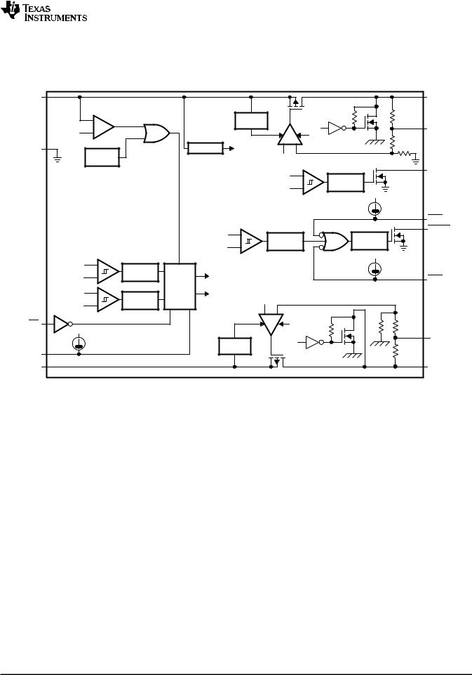
DEVICE INFORMATION
|
|
|
|
Fixed Voltage Version |
|
|
|||
VIN1 (2 Pins) |
|
|
|
|
|
|
|
|
VOUT1 (2 Pins) |
|
|
UVLO1 |
|
|
|
|
|
|
|
|
− |
Comp |
|
|
|
Current |
|
|
10 kΩ |
|
|
|
|
|
|
|
|
|
|
|
|
|
|
|
|
Sense |
|
ENA_1 |
VSENSE1 |
2.5 V |
+ |
|
|
|
|
|
|
|
(see Note A) |
|
|
|
|
|
|
|
− + ENA_1 |
|
|
GND |
Thermal |
|
|
Reference |
Vref |
|
|
FB1 |
|
|
|
|
|
|
Vref |
|
|
||
|
Shutdown |
|
|
|
|
|
|
||
|
|
|
|
|
|
|
|
||
|
|
|
|
|
|
|
FB1 |
− |
PG1 |
|
|
|
|
|
|
|
Rising Edge |
||
|
|
|
|
|
|
|
|
||
|
|
|
|
|
|
|
|
|
|
|
|
|
|
|
|
0.95 x Vref |
+ |
Deglitch |
|
|
|
|
|
|
|
VIN1 |
|||
|
|
|
|
|
|
|
|
PG |
|
|
|
|
|
|
|
|
|
|
|
|
|
|
|
|
|
|
|
Comp |
|
|
|
|
|
|
|
Reset |
|
|
MR2 |
|
|
|
|
|
|
|
|
|
|
|
|
|
|
|
|
Comp |
|
|
RESET |
|
|
|
|
|
FB2 |
− |
Rising Edge |
|
120ms |
|
|
|
|
|
|
|
|||
|
|
|
|
|
|
|
|
||
|
|
|
|
|
0.95 x Vref |
+ |
Deglitch |
|
Delay |
VOUT2 UV Comp |
|
|
|
|
|
||||
|
|
|
|
|
|
VIN1 |
|||
|
|
|
|
|
|
|
|
|
|
FB2 |
|
− |
|
|
|
|
|
|
|
|
|
Falling Edge |
|
|
|
|
|
|
|
|
|
|
|
|
|
|
|
|
|
0.83 x Vref |
|
+ |
Deglitch |
Power |
ENA_1 |
|
|
MR1 |
|
|
|
|
|
|
|
|
|||
|
|
|
|
Sequence |
|
|
|
|
|
FB1 |
|
− |
Falling Edge |
Logic |
ENA_2 |
|
|
|
|
|
|
|
|
|
|||||
|
|
|
|
|
Vref |
|
|
|
|
|
|
+ |
Deglitch |
|
|
|
|
|
|
0.83 x Vref |
|
|
|
|
|
|
|
||
|
|
|
|
|
|
|
|
|
|
VOUT1 UV Comp |
|
|
|
− |
+ |
|
|
||
EN |
|
|
|
|
|
|
ENA_2 |
|
|
VIN1 |
|
|
|
|
|
|
|
|
VSENSE2 |
|
|
|
|
|
|
|
|
|
|
|
|
|
|
|
|
Current |
ENA_2 |
|
(see Note A) |
SEQ |
|
|
|
|
|
Sense |
|
|
10 kΩ |
(see Note B) |
|
|
|
|
|
|
|
|
|
VIN2 (2 Pins) |
|
|
|
|
|
|
|
|
VOUT2 (2 Pins) |
A.For most applications, VSENSE1 and VSENSE2 should be externally connected to VOUT as close as possible to the device. For other implementations, refer to SENSE terminal connection discussion in the Application Information section.
B.If the SEQ terminal is floating at the input, VOUT2 powers up first.
Copyright © 1999–2010, Texas Instruments Incorporated |
Submit Documentation Feedback |
7 |

TPS70145, TPS70148
TPS70151, TPS70158
TPS70102
SLVS222I –DECEMBER 1999–REVISED AUGUST 2010 |
www.ti.com |
Adjustable Voltage Version
VIN1 (2 Pins)
|
UVLO |
|
|
|
|
|
|
Comp |
Current |
|
|
|
|
|
− |
|
|
|
|
|
|
|
Sense |
|
|
ENA_1 |
|
|
|
|
|
|
|
|
2.5 V |
+ |
|
|
|
|
|
|
|
|
− |
+ |
ENA_1 |
|
GND |
Reference |
Vref |
|
|
|
|
|
Thermal |
|
Vref |
|
|
|
|
Shutdown |
|
|
|
|
|
|
|
|
|
|
|
|
|
|
|
FB1 |
|
− |
Rising Edge |
|
|
|
|
|
|
|
|
|
|
0.95 x Vref |
|
+ |
Deglitch |
|
|
|
|
VIN1 |
||
|
|
|
|
|
PG |
|
|
|
|
|
|
Comp |
|
|
|
Reset |
|
|
|
|
|
|
Comp |
|
|
|
|
|
FB2 |
− |
Rising Edge |
|
120ms |
|
|
0.95 x Vref |
+ |
Deglitch |
|
Delay |
|
|
|
|
|
|
||
|
VOUT2 UV Comp |
|
|
|
|
VIN1 |
|
|
|
|
|
|
|
|
|
FB2 |
− |
|
|
|
|
|
|
|
|
|
|
|
|||||||
|
|
|
|
|
|
|
|
|
|
|
|
Falling Edge |
|
|
|
|
ENA_1 |
||||
|
|
|
|
+ |
|
|
|
|
|
|
Deglitch |
|
|
|
|
||||||
|
|
|
|
|
|
|
|
||||||||||||||
|
|
0.83 x Vref |
|
|
|
Power |
|
||||||||||||||
|
|
|
|
|
|
|
|
|
|
|
|
|
|
Sequence |
|
|
|
|
|
|
|
|
|
FB1 |
− |
|
|
|
|
Logic |
|
ENA_2 |
|||||||||||
|
|
|
|
|
|
|
|
|
|
|
|
Falling Edge |
|
|
|
|
|
Vref |
|||
|
|
0.83 x Vref |
|
+ |
|
|
|
|
|
|
Deglitch |
|
|
|
|
|
|||||
|
|
|
|
|
|
|
|
|
|
|
|
|
|
|
|
|
|
|
|
|
|
|
|
|
|
|
|
|
|
|
|
|
|
|
|
|
|
|
|
|
|
|
|
|
|
VOUT1 UV Comp |
|
|
|
|
|
|
|
− + |
|||||||||||
EN |
|
|
|
|
|
|
|
||||||||||||||
|
|
|
|
|
|
|
|
|
|
|
|
|
|
|
|
|
|
ENA_2 |
|||
VIN1 |
|
|
|
|
|
|
|
|
|
|
|
|
|
|
|
|
|
||||
|
|
|
|
|
|
|
|
|
|
|
|
|
|
|
|
|
|
|
|
||
|
Current |
ENA_2 |
SEQ |
Sense |
|
(see Note B) |
|
|
VIN2 (2 Pins) |
|
|
VOUT1 (2 Pins)
FB1
(see Note A)
PG1
MR2
RESET
MR1
FB2
(see Note A)
VOUT2 (2 Pins)
A.For most applications, FB1 and FB2 should be externally connected to resistor dividers as close as possible to the device. For other implementations, refer to FB terminals connection discussion in the Application Information section.
B.If the SEQ terminal is floating at the input, VOUT2 powers up first
8 |
Submit Documentation Feedback |
Copyright © 1999–2010, Texas Instruments Incorporated |

TPS70145, TPS70148
TPS70151, TPS70158
TPS70102
www.ti.com |
SLVS222I –DECEMBER 1999–REVISED AUGUST 2010 |
|
RESET Timing Diagram (with VIN1 Powered Up) |
|||||
VIN2 |
|
|
|
|
|
|
VRES |
|
|
|
|
|
VRES |
(see Note A) |
|
|
|
|
|
t |
|
|
|
|
|
|
|
VOUT2 |
V |
IT + |
(see Note B) |
V |
IT + |
(see Note B) |
Threshold |
|
|
|
|
|
|
Voltage |
|
|
|
|
|
|
|
|
|
VIT − |
|
|
VIT − |
|
|
|
(see Note B) |
|
|
(see Note B) |
|
|
t |
RESET |
120 ms |
120 ms |
Output |
||
|
Delay |
Delay |
Output |
|
Output |
Undefined |
|
Undefined |
|
|
t |
NOTES: A. VRES is the minimum input voltage for a valid RESET. The symbol VRES is not currently listed within EIA or JEDEC standards for semiconductor symbology
B. VIT −T rip voltage is typically 5% lower than the output voltage (95%VO) VIT− to VIT+ is the hysteresis voltage.
PG1 Timing Diagram
VUVLO
VPG1
(see Note A)
VIN1 |
VUVLO |
VPG1 |
t |
VOUT2 |
|
V |
(see Note B) |
|
V (see Note B) |
|
|
||||
|
|
IT + |
|
|
IT+ |
Threshold
Voltage
VIT − |
|
VIT − |
|
||
(see Note B) |
|
(see Note B) |
|
t |
PG1 |
|
Output |
|
Output |
Output |
Undefined |
Undefined |
|
t |
NOTES: A. VPG1 is the minimum input voltage for a valid PG1. The symbol VPG1 is not currently listed within EIA or JEDEC standards for semiconductor symbology.
B. VIT −T rip voltage is typically 5% lower than the output voltage (95%VO) VIT− to VIT+ is the hysteresis voltage.
Copyright © 1999–2010, Texas Instruments Incorporated |
Submit Documentation Feedback |
9 |

TPS70145, TPS70148
TPS70151, TPS70158
TPS70102
SLVS222I –DECEMBER 1999–REVISED AUGUST 2010 www.ti.com
|
|
|
|
|
|
|
Table 1. TERMINAL FUNCTIONS |
|
|
|
|
|
|
|
|
|
|
|
|
TERMINAL |
I/O |
DESCRIPTION |
|
|
|
|
|
|
|
||
|
NAME |
NO. |
|||||
|
|
|
|||||
|
|
|
|
|
|
||
|
|
|
6 |
I |
Active low enable |
||
|
EN |
||||||
|
GND |
8 |
— |
Ground |
|||
|
|
|
|
|
|
|
|
|
|
|
|
4 |
I |
Manual reset input 1, active low, pulled up internally |
|
|
MR1 |
||||||
|
|
|
|
5 |
I |
Manual reset input 2, active low, pulled up internally |
|
|
MR2 |
||||||
|
NC |
1, 11, 20 |
— |
No connection |
|||
|
|
|
|
|
|
|
|
|
PG1 |
16 |
O |
Open drain output, low when VOUT1 voltage is less than 95% of the nominal regulated |
|||
|
|
|
|
|
|
|
voltage |
|
|
|
|
|
15 |
O |
Open drain output, SVS (power-on reset) signal, active low |
|
RESET |
||||||
|
SEQ |
7 |
I |
Power-up sequence control: SEQ = High, VOUT2 powers up first; |
|||
|
|
|
|
|
|
|
SEQ = Low, VOUT1 powers up first, SEQ terminal pulled up internally. |
|
VIN1 |
2, 3 |
I |
Input voltage of regulator 1 |
|||
|
VIN2 |
9, 10 |
I |
Input voltage of regulator 2 |
|||
|
VOUT1 |
18, 19 |
O |
Output voltage of regulator 1 |
|||
|
VOUT2 |
12, 13 |
O |
Output voltage of regulator 2 |
|||
|
VSENSE2/FB2 |
14 |
I |
Regulator 2 output voltage sense/regulator 2 feedback for adjustable |
|||
|
VSENSE1/FB1 |
17 |
I |
Regulator 1 output voltage sense/regulator 1 feedback for adjustable |
|||
Detailed Description
The TPS701xx low dropout regulator family provides dual regulated output voltages for DSP applications that require high-performance power management solutions. These devices provide fast transient response and high accuracy with small output capacitors, while drawing low quiescent current. Programmable sequencing provides a power solution for DSPs without any external component requirements. This architecture reduces the component cost and board space while increasing total system reliability. The TPS701xx family has an enable feature that puts the device in sleep mode reducing the input currents to less than 3mA. Other features are integrated SVS (Power-On Reset, RESET) and Power Good (PG1) that monitor output voltages and provide logic output to the system. These differentiated features provide a complete DSP power solution.
The TPS701xx, unlike many other LDOs, feature very low quiescent current that remains virtually constant even with varying loads. Conventional LDO regulators use a pnp pass element, the base current of which is directly proportional to the load current through the regulator (IB = IC/b). The TPS701xx uses a PMOS transistor to pass current; because the gate of the PMOS is voltage=driven, operating current is low and stable over the full load range.
Pin Functions
Enable
The EN terminal is an input that enables or shuts down the device. If EN is at a voltage high signal, the device is in shutdown mode. When EN goes to voltage low, the device is enabled.
Sequence
The SEQ terminal is an input that programs which output voltage (VOUT1 or VOUT2) is turned on first. When the device is enabled and the SEQ terminal is pulled high or left open, VOUT2 turns on first and VOUT1 remains off until VOUT2 reaches approximately 83% of its regulated output voltage. At that time, VOUT1 is turned on. If VOUT2 is
pulled below 83% (for example, in an overload condition) VOUT1 is turned off. These terminals have a 6-mA pullup current to VIN1.
Pulling the SEQ terminal low reverses the power-up order and VOUT1 is turned on first. For detailed timing diagrams, refer to Figure 40 through Figure 44.
10 |
Submit Documentation Feedback |
Copyright © 1999–2010, Texas Instruments Incorporated |
TPS70145, TPS70148
TPS70151, TPS70158
TPS70102
www.ti.com |
SLVS222I –DECEMBER 1999–REVISED AUGUST 2010 |
Power-Good
The PG1 is an open drain, active high output terminal that indicates the status of the VOUT1 regulator. When the VOUT1 reaches 95% of its regulated voltage, PG1 will go to a high impedance state. It will go to a low impedance state when it is pulled below 95% (for example, during an overload condition) of its regulated voltage. The open
drain output of the PG1 terminal requires a pull-up resistor.
Manual Reset Pins (MR1 and MR2)
MR1 and MR2 are active low input terminals used to trigger a reset condition. When either MR1 or MR2 is pulled to logic low, a POR (RESET) will occur. These terminals have a 6mA pull-up current to VIN1.
Sense (VSENSE1, VSENSE2)
The sense terminals of fixed-output options must be connected to the regulator output, and the connection should be as short as possible. Internally, sense connects to high-impedance, wide-bandwidth amplifiers through a resistor-divider network and noise pickup feeds through to the regulator output. It is essential to route the
sense connection in such a way to minimize or avoid noise pickup. Adding RC networks between the VSENSE terminals and VOUT terminals to filter noise is not recommended because these networks can cause the
regulators to oscillate.
FB1 and FB2
FB1 and FB2 are input terminals used for adjustable-output devices and must be connected to the external feedback resistor divider. FB1 and FB2 connections should be as short as possible. It is essential to route them in such a way as to minimize or avoid noise pickup. Adding RC networks between the FB terminals and VOUT terminals to filter noise is not recommended because these networks cause the regulators to oscillate.
RESET Indicator
The TPS701xx features a RESET (SVS, POR, or Power-On Reset). RESET can be used to drive power-on reset circuitry or a low-battery indicator. RESET is an active low, open drain output that indicates the status of the VOUT2 regulator and both manual reset pins (MR1 and MR2). When VOUT2 exceeds 95% of its regulated voltage,
and MR1 and MR2 are in the high impedance state, RESET will go to a high-impedance state after 120ms delay.
RESET will go to a low-impedance state when VOUT2 is pulled below 95% (for example, an overload condition) of its regulated voltage. To monitor VOUT1, the PG1 output pin can be connected to MR1 or MR2. The open drain
output of the RESET terminal requires a pullup resistor. If RESET is not used, it can be left floating.
VIN1 and VIN2
VIN1 and VIN2 are input to the regulators. Internal bias voltages are powered by VIN1.
VOUT1 and VOUT2
VOUT1 and VOUT2 are output terminals of the LDO.
Copyright © 1999–2010, Texas Instruments Incorporated |
Submit Documentation Feedback |
11 |

TPS70145, TPS70148
TPS70151, TPS70158
TPS70102
SLVS222I –DECEMBER 1999–REVISED AUGUST 2010 |
|
|
www.ti.com |
|
|
TYPICAL CHARACTERISTICS |
|
||
|
|
Table 2. Table of Graphs |
|
|
|
|
|
|
|
|
|
|
|
FIGURE |
|
|
|
|
|
VO |
Output voltage |
|
vs Output current |
Figure 1 to Figure 3 |
|
|
|
||
|
vs Temperature |
Figure 4 to Figure 7 |
||
|
|
|
||
|
|
|
|
|
|
Ground current |
|
vs Junction temperature |
Figure 8 |
|
|
|
|
|
PSRR |
Power-supply rejection ratio |
|
vs Frequency |
Figure 9 to Figure 12 |
|
|
|
|
|
|
Output spectral noise density |
|
vs Frequency |
Figure 13 to Figure 16 |
|
|
|
|
|
ZO |
Output impedance |
|
vs Frequency |
Figure 17 to Figure 20 |
|
Dropout voltage |
|
vs Temperature |
Figure 21 and Figure 22 |
|
|
|
|
|
|
|
vs Input voltage |
Figure 23 and Figure 24 |
|
|
|
|
||
|
|
|
|
|
|
Load transient response |
|
|
Figure 25 and Figure 26 |
|
|
|
|
|
|
Line transient response |
|
|
Figure 27 and Figure 28 |
|
|
|
|
|
VO |
Output voltage and enable voltage |
|
vs Time (start-up) |
Figure 29 and Figure 30 |
|
Equivalent series resistance |
|
vs Output current |
Figure 31 to Figure 38 |
|
|
|
|
|
|
Test circuit for typical regions of stability (equivalent series resistance) performance |
Figure 39 |
||
|
|
|
|
|
<![endif]>VO − Output V oltage − V
TPS70151
OUTPUT VOLTAGE vs
OUTPUT CURRENT
3.300 |
|
|
|
|
|
|
|
|
|
|
|
|
|
|
VIN1 = |
4.3 V |
|
|
|
|
|
|
|
|
|
|
|
|
|
|
|
|
|
|
|
|
|
|
|
||
3.299 |
|
TA = 25°C |
|
|
|
|
|
|
|
|
|
|
|
|
|
VOUT1 |
|
|
|
|
|
|
|
|
|
|
|
3.298 |
|
|
|
|
|
|
|
|
|
|
|
|
|
|
|
|
|
|
|
|
|
|
|
|
|
|
|
3.297 |
|
|
|
|
|
|
|
|
|
|
|
|
|
|
|
|
|
|
|
|
|
|
|
|
|
|
|
3.296 |
|
|
|
|
|
|
|
|
|
|
|
|
|
|
|
|
|
|
|
|
|
|
|
|
|
|
|
3.295 |
|
|
|
|
|
|
|
|
|
|
|
|
|
|
|
|
|
|
|
|
|
|
|
|
|
|
|
3.294 |
|
|
|
|
|
|
|
|
|
|
|
|
|
|
|
|
|
|
|
|
|
|
|
|
|
|
|
3.293 |
|
|
|
|
|
|
|
|
|
|
|
|
|
|
|
|
|
|
|
|
|
|
|
|
|
|
|
3.292 |
|
|
|
|
|
|
|
|
|
|
|
|
|
|
|
|
|
|
|
|
|
|
|
|
|
|
|
0 |
0.1 |
0.2 |
0.3 |
0.4 |
0.5 |
0.6 |
|||||||
IO − Output Current − A
Figure 1.
<![endif]>VO − Output V oltage − V
|
TPS70151 |
|
OUTPUT VOLTAGE |
|
vs |
|
OUTPUT CURRENT |
1.802 |
|
|
VIN2 = 2.8V |
1.801 |
TA = 25°C |
|
VOUT2 |
1.800 |
|
1.799 |
|
1.798 |
|
1.797 |
|
1.796 |
|
1.795
0 |
0.05 |
0.1 |
0.15 |
0.2 |
0.25 |
0.3 |
IO − Output Current − A
Figure 2.
12 |
Submit Documentation Feedback |
Copyright © 1999–2010, Texas Instruments Incorporated |

|
TPS70145, TPS70148 |
|
TPS70151, TPS70158 |
|
TPS70102 |
www.ti.com |
SLVS222I –DECEMBER 1999–REVISED AUGUST 2010 |
TPS70145 |
TPS70151 |
<![endif]>VO − Output V oltage − V
OUTPUT VOLTAGE |
OUTPUT VOLTAGE |
|
|
|
vs |
|
|
|
|
|
|
|
|
vs |
|
|
|
|
|
|
|
OUTPUT CURRENT |
|
|
|
|
|
TEMPERATURE |
|
|
|
|
|||||
1.201 |
|
|
|
|
|
|
3.286 |
VIN1 = 4.3 V |
|
|
|
|
|
|
|
|
|
|
|
|
|
VIN2 = 2.7 V |
|
|
|
|
|
|
|
|
|
|
|||
|
|
|
|
TA = 25°C |
|
3.284 |
IO = 1 mA |
|
|
|
|
|
|
|
|
||
1.200 |
|
|
|
VOUT2 |
|
3.282 |
VOUT1 |
|
|
|
|
|
|
|
|
|
|
|
|
|
|
|
|
|
|
|
|
|
|
|
|
|
|
|
|
1.199 |
|
|
|
|
|
<![if ! IE]> <![endif]>− V |
3.280 |
|
|
|
|
|
|
|
|
|
|
|
|
|
|
|
<![if ! IE]> <![endif]>oltage |
|
|
|
|
|
|
|
|
|
|
||
|
|
|
|
|
|
3.278 |
|
|
|
|
|
|
|
|
|
|
|
1.198 |
|
|
|
|
|
<![if ! IE]> <![endif]>V |
|
|
|
|
|
|
|
|
|
|
|
|
|
|
|
|
<![if ! IE]> <![endif]>Output− |
3.276 |
|
|
|
|
|
|
|
|
|
|
|
|
|
|
|
|
|
|
|
|
|
|
|
|
|
|
|
||
|
|
|
|
|
|
|
|
|
|
|
|
|
|
|
|
|
|
1.197 |
|
|
|
|
|
<![if ! IE]> <![endif]>O |
3.274 |
|
|
|
|
|
|
|
|
|
|
|
|
|
|
|
|
|
|
|
|
|
|
|
|
|
|
|
|
|
|
|
|
|
|
<![if ! IE]> <![endif]>V |
|
|
|
|
|
|
|
|
|
|
|
|
|
|
|
|
|
|
3.272 |
|
|
|
|
|
|
|
|
|
|
1.196 |
|
|
|
|
|
|
3.270 |
|
|
|
|
|
|
|
|
|
|
|
|
|
|
|
|
|
|
|
|
|
|
|
|
|
|
|
|
1.195 |
|
|
|
|
|
|
3.268 |
|
|
|
|
|
|
|
|
|
|
0 |
0.05 |
0.1 |
0.15 |
0.2 |
0.25 |
0.3 |
−40 −25 −10 |
5 |
20 |
35 |
50 |
65 |
80 |
95 |
110 |
125 |
|
|
|
IO − Output Current − A |
|
|
|
|
|
T − T emperature − °C |
|
|
|
||||||
Figure 3. |
Figure 4. |
TPS70151
OUTPUT VOLTAGE vs TEMPERATURE
|
3.288 |
|
|
|
|
|
VIN1 = 4.3 V |
|
||
|
|
|
|
|
|
|
|
|||
|
3.286 |
|
|
|
|
|
IO = 500 mA |
|
||
|
|
|
|
|
|
|
VOUT1 |
|
|
|
|
3.284 |
|
|
|
|
|
|
|
|
|
| <![if ! IE]> <![endif]>− V |
3.282 |
|
|
|
|
|
|
|
|
|
| <![if ! IE]> <![endif]>oltage |
|
|
|
|
|
|
|
|
|
|
3.280 |
|
|
|
|
|
|
|
|
|
|
| <![if ! IE]> <![endif]>V |
|
|
|
|
|
|
|
|
|
|
| <![if ! IE]> <![endif]>− Output |
3.278 |
|
|
|
|
|
|
|
|
|
3.276 |
|
|
|
|
|
|
|
|
|
|
| <![if ! IE]> <![endif]>O |
|
|
|
|
|
|
|
|
|
|
|
|
|
|
|
|
|
|
|
|
|
| <![if ! IE]> <![endif]>V |
3.274 |
|
|
|
|
|
|
|
|
|
|
|
|
|
|
|
|
|
|
|
|
|
3.272 |
|
|
|
|
|
|
|
|
|
|
3.270 |
|
|
|
|
|
|
|
|
|
|
−40 −25 −10 |
5 |
20 |
35 |
50 |
65 |
80 |
95 |
110 |
125 |
|
|
|
T − T emperature − °C |
|
|
|
||||
Figure 5.
TPS70151
OUTPUT VOLTAGE vs TEMPERATURE
|
1.800 |
|
|
|
|
|
|
|
|
|
|
|
|
VIN2 = 2.8 V |
|
|
|
|
|
|
|
|
|
|
1.798 |
IO = 1 mA |
|
|
|
|
|
|
|
|
|
|
VOUT2 |
|
|
|
|
|
|
|
|
|
|
| <![if ! IE]> <![endif]>V |
1.796 |
|
|
|
|
|
|
|
|
|
|
| <![if ! IE]> <![endif]>− |
|
|
|
|
|
|
|
|
|
|
|
| <![if ! IE]> <![endif]>V oltage |
1.794 |
|
|
|
|
|
|
|
|
|
|
|
|
|
|
|
|
|
|
|
|
|
|
| <![if ! IE]> <![endif]>− Output |
1.792 |
|
|
|
|
|
|
|
|
|
|
|
|
|
|
|
|
|
|
|
|
|
|
| <![if ! IE]> <![endif]>O |
1.790 |
|
|
|
|
|
|
|
|
|
|
| <![if ! IE]> <![endif]>V |
|
|
|
|
|
|
|
|
|
|
|
|
|
|
|
|
|
|
|
|
|
|
|
|
1.788 |
|
|
|
|
|
|
|
|
|
|
|
1.786 |
|
|
|
|
|
|
|
|
|
|
|
−40 −25 −10 |
5 |
20 |
35 |
50 |
65 |
80 |
95 |
110 |
125 |
|
|
|
|
|
T − T emperature − °C |
|
|
|
||||
Figure 6.
Copyright © 1999–2010, Texas Instruments Incorporated |
Submit Documentation Feedback |
13 |
Loading...