


 Loading...
Texas Instruments TPS2020D, TPS2021D, TPS2021P, TPS2022D, TPS2023D Schematic [ru]
...TPS2020, TPS2021
TPS2022, TPS2023, TPS2024
www.ti.com
SLVS175C –DECEMBER 1998–REVISED SEPTEMBER 2007
POWER-DISTRIBUTION SWITCHES
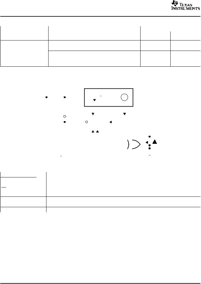
FEATURES |
∙ UL Listed - File No. E169910 |
∙33-mΩ (5-V Input) High-Side MOSFET Switch
∙ |
Short-Circuit and Thermal Protection |
|
D OR P PACKAGE |
||||||||
|
|
|
|
(TOP VIEW) |
|
|
|
|
|||
∙ |
Overcurrent Logic Output |
GND |
|
|
|
|
OUT |
||||
|
1 |
8 |
|
||||||||
∙ |
Operating Range . . . 2.7 V to 5.5 V |
|
|
||||||||
|
IN |
|
2 |
7 |
|
OUT |
|||||
∙ |
Logic-Level Enable Input |
|
|
|
|||||||
|
IN |
|
|
|
|
OUT |
|||||
|
|
3 |
6 |
|
|||||||
∙ |
Typical Rise Time . . . 6.1 ms |
|
|
|
|||||||
|
|
|
|
4 |
5 |
|
|
|
|
||
|
EN |
|
|
|
|
OC |
|
||||
∙Undervoltage Lockout
∙Maximum Standby Supply Current . . . 10 μA
∙No Drain-Source Back-Gate Diode
∙Available in 8-Pin SOIC and PDIP Packages
∙Ambient Temperature Range, –40°C to 85°C
∙2-kV Human-Body-Model, 200-V Machine-Model ESD Protection
DESCRIPTION
The TPS202x family of power distribution switches is intended for applications where heavy capacitive loads and short circuits are likely to be encountered. These devices are 50-mΩ N-channel MOSFET high-side power switches. The switch is controlled by a logic enable compatible with 5-V logic and 3-V logic. Gate drive is provided by an internal charge pump designed to control the power-switch rise times and fall times to minimize current surges during switching. The charge pump requires no external components and allows operation from supplies as low as 2.7 V.
When the output load exceeds the current-limit threshold or a short is present, the TPS202x limits the output current to a safe level by switching into a constant-current mode, pulling the overcurrent (OC) logic output low. When continuous heavy overloads and short circuits increase the power dissipation in the switch, causing the junction temperature to rise, a thermal protection circuit shuts off the switch to prevent damage. Recovery from a thermal shutdown is automatic once the device has cooled sufficiently. Internal circuitry ensures the switch remains off until valid input voltage is present.
The TPS202x devices differ only in short-circuit current threshold. The TPS2020 limits at 0.3-A load, the TPS2021 at 0.9-A load, the TPS2022 at 1.5-A load, the TPS2023 at 2.2-A load, and the TPS2024 at 3-A load (see Available Options). The TPS202x is available in an 8-pin small-outline integrated-circuit (SOIC) package and in an 8-pin dual in-line package (DIP) and operates over a junction temperature range of –40°C to 125°C.
Please be aware that an important notice concerning availability, standard warranty, and use in critical applications of Texas Instruments semiconductor products and disclaimers thereto appears at the end of this data sheet.
PRODUCTION DATA information is current as of publication date. |
Copyright © 1998–2007, Texas Instruments Incorporated |
|
Products conform to specifications per the terms of the Texas |
||
|
||
Instruments standard warranty. Production processing does not |
|
|
necessarily include testing of all parameters. |
|
TPS2020, |
TPS2021 |
TPS2022, |
TPS2023, TPS2024 |
www.ti.com
SLVS175C –DECEMBER 1998–REVISED SEPTEMBER 2007
Table 1. AVAILABLE OPTIONS
|
|
RECOMMENDED MAXIMUM |
TYPICAL SHORT-CIRCUIT |
PACKAGED DEVICES |
|
TA |
ENABLE |
CONTINUOUS LOAD |
CURRENT LIMIT AT 25°C |
SMALL OUTLINE |
PLASTIC DIP |
|
|
CURRENT (A) |
(A) |
(D)(1) |
(P) |
|
|
0.2 |
0.3 |
TPS2020D |
TPS2020P |
|
|
0.6 |
0.9 |
TPS2021D |
TPS2021P |
–40°C to 85°C |
Active low |
1 |
1.5 |
TPS2022D |
TPS2022P |
|
|
1.5 |
2.2 |
TPS2023D |
TPS2023P |
|
|
2 |
3 |
TPS2024D |
TPS2024P |
(1)The D package is available taped and reeled. Add an R suffix to device type (e.g., TPS2020DR)
TPS2020 FUNCTIONAL BLOCK DIAGRAM
|
|
|
|
|
|
|
|
|
|
|
|
|
|
|
Power Switch |
|
|
|
|
|
|
|
|
|
|
|
|
|
|
|
|
|
|
|
|
|
|
|
|||||||||||||
|
|
|
|
|
|
|
|
|
|
|
|
|
|
|
|
|
|
|
|
|
|
|
|
|
|
|
|
|
|
|
|
† |
|
|
|
|
|
|
|
|
|
|
|
|
|
|
|||||
|
|
|
|
|
|
|
|
|
|
|
|
|
|
|
|
|
|
|
|
|
|
|
|
|
|
|
|
|
|
|
|
|
|
|
|
|
|
|
|
|
|
|
|
|
|
||||||
|
|
|
|
|
|
|
|
|
|
|
|
|
|
|
|
|
|
|
|
|
|
|
|
|
|
|
|
|
|
|
|
|
|
|
|
|
|
|
|
|
|
|
|
|
|
||||||
|
|
|
|
IN |
|
|
|
|
|
|
|
|
|
|
|
|
|
|
|
|
|
|
|
|
|
|
|
|
|
CS |
|
|
|
|
|
|
|
|
|
|
|
|
|
|
|
|
|
OUT |
|||
|
|
|
|
|
|
|
|
|
|
|
|
|
|
|
|
|
|
|
|
|
|
|
|
|
|
|
|
|
|
|
|
|
|
|
|
|
|
|
|
|
|
|
|
|
|||||||
|
|
|
|
|
|
|
|
|
|
|
|
|
|
|
|
|
|
|
|
|
|
|
|
|
|
|
|
|
|
|
|
|
|
|
|
|
|
|
|
|
|
|
|
|
|
|
|
|
|||
|
|
|
|
|
|
|
|
|
|
|
|
|
|
|
|
|
|
|
|
|
|
|
|
|
|
|
|
|
|
|
|
|
|
|
|
|
|
|
|
|
|
|
|
|
|
|
|
|
|
|
|
|
|
|
|
|
|
|
|
|
|
|
|
|
|
|
|
|
|
|
|
|
|
|
|
|
|
|
|
|
|
|
|
|
|
|
|
|
|
|
|
|
|
|
|
|
|
|
|
|
|
|
|
|
|
|
|
|
|
|
|
|
Charge |
|
|
|
|
|
|
|
|
|
|
|
|
|
|
|
|
|
|
|
|
|
|
|
|
|
|
|
|
|
|
|
|
||||||||||
|
|
|
|
|
|
|
|
|
|
Pump |
|
|
|
|
|
|
|
|
|
|
|
|
|
|
|
|
|
|
|
|
|
|
|
|
|
|
|
|
|
|
|
|
|||||||||
|
|
|
|
|
|
|
|
|
|
|
|
|
|
|
|
|
|
|
|
|
|
|
|
|
|
|
|
|
|
|
|
|
|
|
|
|
|
|
|
|
|
|
|
|
|
|
|||||
|
|
|
|
|
|
|
|
|
|
|
|
|
|
|
|
|
|
|
|
|
|
|
|
|
|
|
|
|
|
|
|
|
|
|
|
|
|
|
|
|
|
|
|
|
|
|
|
|
|
|
|
|
|
|
|
|
|
|
|
|
|
|
|
|
|
|
|
|
|
|
|
|
|
|
|
|
|
|
|
|
|
Current |
|
|
|
|
|
|
|
|
|
|
|
|
|
|
|
|
|||||
|
|
|
|
EN |
|
|
|
|
|
|
|
|
|
|
|
|
|
Driver |
|
|
|
|
|
|
|
|
|
|
|
|
|
|
|||||||||||||||||||
|
|
|
|
|
|
|
|
|
|
|
|
|
|
|
|
|
|
Limit |
|
|
|
|
|
|
|
|
|
|
|
|
|
|
|
|
|||||||||||||||||
|
|
|
|
|
|
|
|
|
|
|
|
|
|
|
|
|
|
|
|
|
|
|
|
|
|
|
|
|
|
|
|
|
|
|
|
|
|
|
|
|
|
|
|
|
|
||||||
|
|
|
|
|
|
|
|
|
|
|
|
|
|
|
|
|
|
|
|
|
|
|
|
|
|
|
|
|
|
|
|
|
|
|
|
|
|
|
|
|
|
|
|
|
|
|
|
|
|
|
|
|
|
|
|
|
|
|
|
|
|
UVLO |
|
|
|
|
|
|
|
|
|
|
|
|
|
|
|
|
|
|
|
|
|
|
|
|
|
|
|
|
|
|
|
|
|
|
|
OC |
|
||||
|
|
|
|
|
|
|
|
|
|
|
|
|
|
|
|
|
|
|
|
|
|
|
|
|
|
|
|
|
|
|
|
|
|
|
|
|
|
|
|
|
|
||||||||||
|
|
|
|
|
|
|
|
|
|
|
|
|
|
|
|
|
|
|
|
|
|
|
|
|
|
|
|
|
|
|
|
|
|
|
|
|
|
|
|
|
|
||||||||||
|
|
|
|
|
|
|
|
|
|
|
|
|
|
|
|
|
|
|
|
|
|
|
|
|
|
|
|
|
|
|
|
|
|
|
|
|
|
|
|
|
|
|
|
|
|
|
|
|
|
|
|
|
|
|
GND |
|
|
|
|
|
|
|
|
|
|
|
|
Thermal |
|
|
|
|
|
|
|
|
|
|
|
|
|
|
|
|
|
|
|
|
|
|
|
||||||||||||
|
|
|
|
|
|
|
|
|
|
|
|
|
|
|
|
Sense |
|
|
|
|
|
|
|
|
|
|
|
|
|
|
|
|
|
|
|
|
|
|
|
||||||||||||
|
|
|
|
|
|
|
|
|
|
|
|
|
|
|
|
|
|
|
|
|
|
|
|
|
|
|
|
|
|
|
|
|
|
|
|
|
|
|
|
|
|
|
|
|
|
|
|
||||
|
|
|
|
|
|
|
|
|
|
|
|
|
|
|
|
|
|
|
|
|
|
|
|
|
|
|
|
|
|
|
|
|
|
|
|
|
|
|
|
|
|
|
|
|
|
|
|
|
|
|
|
|
|
|
† Current Sense |
|
|
|
|
|
|
|
|
|
|
|
|
|
|
|
|
|
|
|
|
|
|
|
|||||||||||||||||||||||||
|
|
|
|
|
|
|
|
|
|
|
|
|
|
|
TERMINAL FUNCTIONS |
|
|
|
|
|
|
|
|
|
|
|
|
|
|
||||||||||||||||||||||
|
TERMINAL |
|
|
|
|
|
|
|
|
|
|
|
|
|
|
|
|
|
|
|
|
|
|
|
|
|
|
|
|
|
|
|
|
|
|
|
|
|
|
|
|
|
|
|
|
|
|
|
|
|
|
NAME |
NO. |
|
I/O |
|
|
|
|
|
|
|
|
|
|
|
|
|
|
|
|
|
|
|
|
|
|
DESCRIPTION |
|
|
|
|
|
|
|
|
|
|
|
|
|
|
|||||||||||
D OR P |
|
|
|
|
|
|
|
|
|
|
|
|
|
|
|
|
|
|
|
|
|
|
|
|
|
|
|
|
|
|
|
|
|
|
|
|
|
|
|
|
|
|
|
|
|
|
|
|
|
||
|
|
|
|
|
|
|
|
|
|
|
|
|
|
|
|
|
|
|
|
|
|
|
|
|
|
|
|
|
|
|
|
|
|
|
|
|
|
|
|
|
|
|
|
|
|
|
|
|
|
|
|
EN |
|
4 |
|
|
I |
Enable input. Logic-low turns on power switch. |
|
|
|
|
|
|
|
|
|
|
|
|
|
|
|||||||||||||||||||||||||||||||
GND |
|
1 |
|
|
I |
Ground |
|
|
|
|
|
|
|
|
|
|
|
|
|
|
|
|
|
|
|
|
|
|
|
||||||||||||||||||||||
IN |
|
2, 3 |
|
|
I |
Input voltage |
|
|
|
|
|
|
|
|
|
|
|
|
|
|
|
|
|
|
|
|
|
|
|
||||||||||||||||||||||
OC |
|
5 |
|
O |
Overcurrent. Logic output, active-low |
|
|
|
|
|
|
|
|
|
|
|
|
|
|
|
|
|
|
|
|
|
|
|
|||||||||||||||||||||||
OUT |
|
6, 7, 8 |
|
O |
Power-switch output |
|
|
|
|
|
|
|
|
|
|
|
|
|
|
|
|
|
|
|
|
|
|
|
|||||||||||||||||||||||
2 |
Submit Documentation Feedback |
Copyright © 1998–2007, Texas Instruments Incorporated |
|
Product Folder Link(s): TPS2020 TPS2021 TPS2022 TPS2023 TPS2024 |
|
TPS2020, TPS2021
TPS2022, TPS2023, TPS2024
www.ti.com
SLVS175C –DECEMBER 1998–REVISED SEPTEMBER 2007
DETAILED DESCRIPTION
POWER SWITCH
The power switch is an N-channel MOSFET with a maximum on-state resistance of 50 mΩ (VI(IN) = 5 V). Configured as a high-side switch, the power switch prevents current flow from OUT to IN and IN to OUT when
disabled.
CHARGE PUMP
An internal charge pump supplies power to the driver circuit and provides the necessary voltage to pull the gate of the MOSFET above the source. The charge pump operates from input voltages as low as 2.7 V and requires very little supply current.
DRIVER
The driver controls the gate voltage of the power switch. To limit large current surges and reduce the associated electromagnetic interference (EMI) produced, the driver incorporates circuitry that controls the rise times and fall times of the output voltage. The rise and fall times are typically in the 2-ms to 9-ms range.
ENABLE (EN)
The logic enable disables the power switch, the bias for the charge pump, driver, and other circuitry to reduce the supply current to less than 10 μA when a logic-high is present on EN. A logic-zero input on EN restores bias to the drive and control circuits and turns the power on. The enable input is compatible with both TTL and CMOS logic levels.
OVERCURRENT (OC)
The OC open drain output is asserted (active low) when an overcurrent or overtemperature condition is encountered. The output remains asserted until the overcurrent or overtemperature condition is removed.
CURRENT SENSE
A sense FET monitors the current supplied to the load. The sense FET measures current more efficiently than conventional resistance methods. When an overload or short circuit is encountered, the current-sense circuitry sends a control signal to the driver. The driver, in turn, reduces the gate voltage and drives the power FET into its saturation region, which switches the output into a constant-current mode and holds the current constant while varying the voltage on the load.
THERMAL SENSE
An internal thermal-sense circuit shuts off the power switch when the junction temperature rises to approximately 140°C. Hysteresis is built into the thermal sense circuit. After the device has cooled approximately 20°C, the switch turns back on. The switch continues to cycle off and on until the fault is removed.
UNDERVOLTAGE LOCKOUT
A voltage sense circuit monitors the input voltage. When the input voltage is below approximately 2 V, a control signal turns off the power switch.
Copyright © 1998–2007, Texas Instruments Incorporated |
Submit Documentation Feedback |
3 |
Product Folder Link(s): TPS2020 TPS2021 TPS2022 TPS2023 TPS2024
TPS2020, TPS2021
TPS2022, TPS2023, TPS2024
www.ti.com
SLVS175C –DECEMBER 1998–REVISED SEPTEMBER 2007
ABSOLUTE MAXIMUM RATINGS
over operating free-air temperature range (unless otherwise noted)(1)
 VI(IN) (2)
VO(OUT) (2)
VI(EN)
IO(OUT)
 TJ
TJ
Tstg
Input voltage range |
|
–0.3 V to 6 V |
Output voltage range |
|
–0.3 V to VI(IN) + 0.3 V |
Input voltage range |
|
–0.3 V to 6 V |
Continuous output current |
|
Internally limited |
Continuous total power dissipation |
|
See Dissipation Rating Table |
Operating virtual junction temperature range |
|
–40°C to 125°C |
Storage temperature range |
|
–65°C to 150°C |
Lead temperature soldering 1,6 mm (1/16 inch) from case for 10 seconds |
260°C |
|
Electrostatic discharge (ESD) protection: |
Human body model |
2 kV |
|
Machine model |
200 V |
|
Charged device model (CDM) |
750 V |
(1)Stresses beyond those listed under absolute maximum ratings may cause permanent damage to the device. These are stress ratings only, and functional operation of the device at these or any other conditions beyond those indicated under recommended operating conditions is not implied. Exposure to absolute-maximum-rated conditions for extended periods may affect device reliability.
(2)All voltages are with respect to GND.
DISSIPATION RATING TABLE
PACKAGE |
TA ≤ 25°C |
DERATING FACTOR |
TA = 70°C |
TA = 85°C |
|
POWER RATING |
ABOVE TA = 25°C |
POWER RATING |
POWER RATING |
||
|
|||||
D |
725 mW |
5.8 mW/°C |
464 mW |
377 mW |
|
P |
1175 mW |
9.4 mW/°C |
752 mW |
611 mW |
RECOMMENDED OPERATING CONDITIONS
|
|
|
MIN |
MAX |
UNIT |
VI(IN) |
Input voltage |
|
2.7 |
5.5 |
V |
VI(EN) |
|
0 |
5.5 |
V |
|
|
|
||||
|
|
TPS2020 |
0 |
0.2 |
|
|
|
TPS2021 |
0 |
0.6 |
|
IO |
Continuous output current |
TPS2022 |
0 |
1 |
A |
|
|
TPS2023 |
0 |
1.5 |
|
|
|
TPS2024 |
0 |
2 |
|
TJ |
Operating virtual junction temperature |
|
–40 |
125 |
°C |
4 |
Submit Documentation Feedback |
Copyright © 1998–2007, Texas Instruments Incorporated |
|
Product Folder Link(s): TPS2020 TPS2021 TPS2022 TPS2023 TPS2024 |
|
TPS2020, TPS2021
TPS2022, TPS2023, TPS2024
www.ti.com
SLVS175C –DECEMBER 1998–REVISED SEPTEMBER 2007
ELECTRICAL CHARACTERISTICS
over recommended operating junction temperature range, VI(IN) = 5.5 V, IO = rated current, EN = 0 V (unless otherwise noted)
|
PARAMETER |
TEST CONDITIONS(1) |
MIN TYP |
MAX UNIT |
|
POWER SWITCH |
|
|
|
||
|
|
VI(IN) = 5 V, TJ = 25°C, IO = 1.8 A |
33 |
36 |
|
|
|
VI(IN) = 5 V, TJ = 85°C, IO = 1.8 A |
38 |
46 |
|
|
|
VI(IN) = 5 V, TJ = 125°C, IO = 1.8 A |
44 |
50 |
|
|
|
VI(IN) = 3.3 V, TJ = 25°C, IO = 1.8 A |
37 |
41 |
|
|
|
VI(IN) = 3.3 V, TJ = 85°C, IO = 1.8 A |
43 |
52 |
|
rDS(on) |
Static drain-source on-state |
VI(IN) = 3.3 V, TJ = 125°C, IO = 1.8 A |
51 |
61 |
|
resistance |
VI(IN) = 5 V, TJ = 25°C, IO = 0.18 A |
30 |
mΩ |
||
|
34 |
||||
|
|
VI(IN) = 5 V, TJ = 85°C, IO = 0.18 A |
35 |
41 |
|
|
|
VI(IN) = 5 V, TJ = 125°C, IO = 0.18 A |
39 |
47 |
|
|
|
VI(IN) = 3.3 V, TJ = 25°C, IO = 0.18 A |
33 |
37 |
|
|
|
VI(IN) = 3.3 V, TJ = 85°C, IO = 0.18 A |
39 |
46 |
|
|
|
VI(IN) = 3.3 V, TJ = 125°C, IO = 0.18 A |
44 |
56 |
|
tr |
Rise time, output |
VI(IN) = 5.5 V, CL = 1 μF, TJ = 25°C, RL = 10 Ω |
6.1 |
ms |
|
VI(IN) = 2.7 V, CL = 1 μF, TJ = 25°C, RL = 10 Ω |
8.6 |
||||
|
|
|
|||
tf |
Fall time, output |
VI(IN) = 5.5 V, CL = 1 μF, TJ = 25°C, RL = 10 Ω |
3.4 |
ms |
|
VI(IN) = 2.7 V, CL = 1 μF, TJ = 25°C, RL = 10 Ω |
3 |
||||
|
|
|
|||
ENABLE INPUT (EN) |
|
|
||
VIH |
High-level input voltage |
2.7 V≤ VI(IN) ≤ 5.5 V |
||
VIL |
Low-level input voltage |
4.5 V ≤ VI(IN) ≤ 5.5 V |
||
2.7 V ≤ VI(IN) ≤ 4.5 V |
||||
|
|
|||
II |
Input current |
EN= 0 V or EN = VI(IN) |
||
ton |
Turnon time |
CL = 100 μF, RL= 10 Ω |
||
toff |
Turnoff time |
CL = 100 μF, RL= 10 Ω |
||
CURRENT LIMIT |
|
|
||
|
|
TJ = 25°C, VI = 5.5 V, |
||
IOS |
Short-circuit output current |
OUT connected to GND, |
||
|
|
Device enabled into short circuit |
||
SUPPLY CURRENT |
|
|
||
Supply current, low-level output |
No load on OUT |
EN = VI(IN) |
||
Supply current, high-level output |
No load on OUT |
EN = 0 V |
||
Leakage current |
OUT connected |
EN = VI(IN) |
||
to ground |
||||
UNDERVOLTAGE LOCKOUT |
|
|
||
Low-level input voltage |
|
|
||
Hysteresis |
|
TJ = 25°C |
|
|
TPS2020
TPS2021
TPS2022
TPS2023
TPS2024
TJ = 25°C
–40°C ≤ TJ ≤ 125°C
TJ = 25°C
–40°C ≤ TJ ≤ 125°C
 –40°C ≤ TJ ≤ 125°C
2 |
|
|
V |
|
|
0.8 |
V |
|
|
0.5 |
|
|
|
|
|
–0.5 |
|
0.5 |
μA |
|
|
20 |
ms |
|
|
40 |
|
|
|
|
|
0.22 |
0.3 |
0.4 |
|
0.66 |
0.9 |
1.1 |
|
1.1 |
1.5 |
1.8 |
A |
1.65 |
2.2 |
2.7 |
|
2.2 |
3 |
3.8 |
|
|
0.3 |
1 |
|
|
|
10 |
μA |
|
|
|
|
|
58 |
75 |
|
|
75 |
100 |
μA |
|
|
||
|
10 |
|
μA |
2 |
|
2.5 |
V |
|
100 |
|
mV |
OVERCURRENT (OC) |
|
|
|
Output low voltage |
IO = 10 mA, VOL(OC) |
0.4 |
V |
Off-state current(2) |
VO = 5 V, VO = 3.3 V |
1 |
μA |
(1)Pulse-testing techniques maintain junction temperature close to ambient temperature; thermal effects must be taken into account separately.
(2)Specified by design, not production tested.
Copyright © 1998–2007, Texas Instruments Incorporated |
Submit Documentation Feedback |
5 |
Product Folder Link(s): TPS2020 TPS2021 TPS2022 TPS2023 TPS2024
TPS2020, TPS2021
TPS2022, TPS2023, TPS2024
www.ti.com
SLVS175C –DECEMBER 1998–REVISED SEPTEMBER 2007
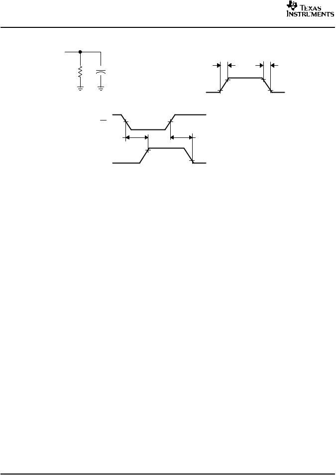
PARAMETER MEASURMENT INFORMATION
OUT
RL |
CL |
|
|
tr |
tf |
|
|
|
|
||
|
|
|
VO(OUT) |
90% |
90% |
|
|
|
|
10% |
10% |
TEST CIRCUIT |
|
|
|
|
|
VI(EN) |
|
50% |
50% |
|
|
|
ton |
|
toff |
|
|
VO(OUT) |
|
|
90% |
|
|
|
|
|
10% |
|
|
VOLTAGE WAVEFORMS
Figure 1. Test Circuit and Voltage Waveforms
6 |
Submit Documentation Feedback |
Copyright © 1998–2007, Texas Instruments Incorporated |
Product Folder Link(s): TPS2020 TPS2021 TPS2022 TPS2023 TPS2024
TPS2020, TPS2021
TPS2022, TPS2023, TPS2024
www.ti.com
SLVS175C –DECEMBER 1998–REVISED SEPTEMBER 2007
PARAMETER MEASURMENT INFORMATION (continued)
TABLE OF TIMING DIAGRAMS
|
FIGURE |
|
Turnon Delay and Rise TIme |
2 |
|
Turnoff Delay and Fall Time |
3 |
|
Turnon Delay and Rise TIme with 1-μF Load |
4 |
|
Turnoff Delay and Rise TIme with 1-μF Load |
5 |
|
Device Enabled into Short |
6 |
|
TPS2020, TPS2021, TPS2022, TPS2023, and TPS2024, Ramped Load on Enabled Device |
7, 8, 9, 10, |
|
11 |
||
|
||
TPS2024, Inrush Current |
12 |
|
7.9-Ω Load Connected to an Enabled TPS2020 Device |
13 |
|
3.7-Ω Load Connected to an Enabled TPS2020 Device |
14 |
|
3.7-Ω Load Connected to an Enabled TPS2021 Device |
15 |
|
2.6-Ω Load Connected to an Enabled TPS2021 Device |
16 |
|
2.6-Ω Load Connected to an Enabled TPS2022 Device |
17 |
|
1.2-Ω Load Connected to an Enabled TPS2022 Device |
18 |
|
1.2-Ω Load Connected to an Enabled TPS2023 Device |
19 |
|
0.9-Ω Load Connected to an Enabled TPS2023 Device |
20 |
|
0.9-Ω Load Connected to an Enabled TPS2024 Device |
21 |
|
0.5-Ω Load Connected to an Enabled TPS2024 Device |
22 |
|
|
|
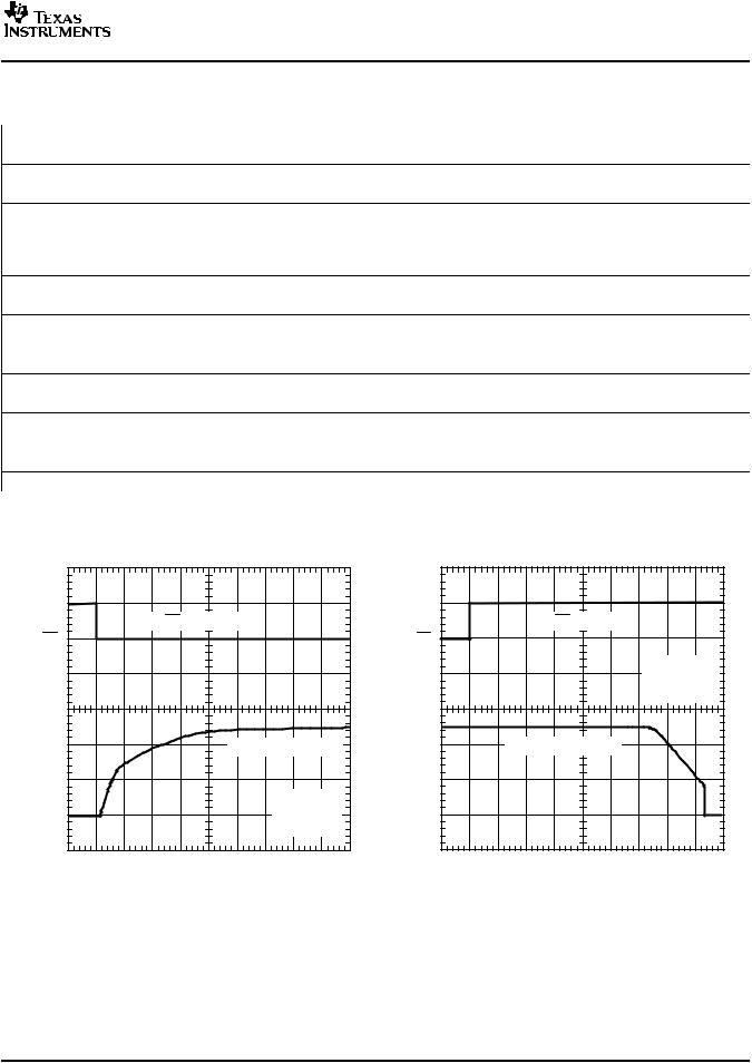
VI(EN) (5 V/div) |
|
|
|
|
|||
VI(EN) |
|
|
|
|
|
|
|
|
|
|
|
|
|
|
|
|
VO(OUT) (2 V/div) |
|
|||
|
|
|
|
|
|
|
|
VIN = 5 V |
|
|
V |
|
|
|
|
|
|
|
RL = 27 Ω |
|
|
O(OUT) |
|
|
|
|
|
|
|
TA = 25°C |
|
|
|
|
|
|
|
|
|
|
|
||
0 |
2 |
4 |
6 |
8 |
10 |
12 |
14 |
16 |
18 |
20 |
|
|
|
|
t − T ime − ms |
|
|
|
|
||
|
|
Figure 2. Turnon Delay and Rise Time |
|
|||||||
|
|
|
|
VI(EN) (5 V/div) |
|
|
|
|
||
VI(EN) |
|
|
|
|
|
|
|
|
|
|
|
|
|
|
|
|
|
|
VI(IN) = 5 V |
|
|
|
|
|
|
|
|
|
|
RL = 27 Ω |
|
|
|
|
|
|
|
|
|
|
TA = 25°C |
|
|
|
|
|
VO(OUT) (2 V/div) |
|
|
|
|
|
||
VO(OUT) |
|
|
|
|
|
|
|
|
|
|
0 |
2 |
4 |
6 |
8 |
10 |
12 |
14 |
16 |
18 |
20 |
|
|
|
|
t − T ime − ms |
|
|
|
|
||
|
|
Figure 3. Turnoff Delay and Fall Time |
|
|||||||
Copyright © 1998–2007, Texas Instruments Incorporated |
Submit Documentation Feedback |
7 |
Product Folder Link(s): TPS2020 TPS2021 TPS2022 TPS2023 TPS2024

TPS2020, TPS2021 |
|
|
|
|
|
|
|
|||
TPS2022, TPS2023, TPS2024 |
|
|
|
|
|
|||||
SLVS175C –DECEMBER 1998–REVISED SEPTEMBER 2007 |
|
|
||||||||
|
|
|
|
VI(EN) (5 V/div) |
|
|
|
|
||
VI(EN) |
|
|
|
|
|
|
|
|
|
|
|
|
|
|
|
VO(OUT) (2 V/div) |
|
|
|||
|
|
|
|
|
|
|
|
VI(IN) = 5 V |
|
|
|
|
|
|
|
|
|
|
CL = 1 µF |
|
|
VO(OUT) |
|
|
|
|
|
|
|
RL = 27 Ω |
|
|
|
|
|
|
|
|
|
|
TA = 25°C |
|
|
0 |
2 |
4 |
6 |
8 |
10 |
12 |
14 |
16 |
18 |
20 |
|
|
|
|
t − T ime − ms |
|
|
|
|
||
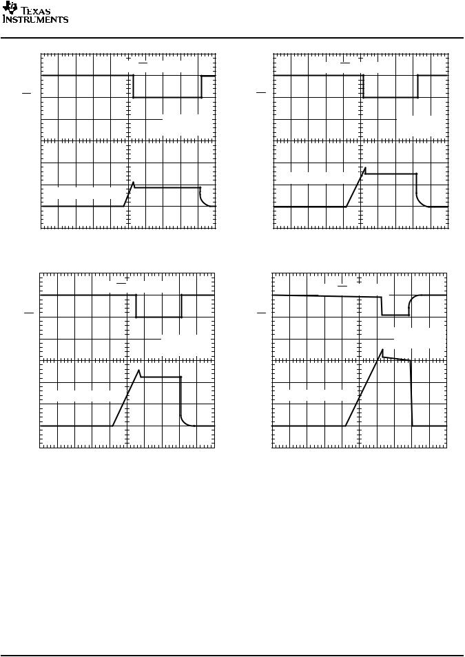
Figure 4. Turnon Delay and Rise Time with 1-μF Load
VI(EN) |
|
|
|
VI(EN) (5 V/div) |
|
|
|
|
||
|
|
|
|
|
|
|
|
|||
|
VI(IN) = 5 V |
|
|
|
|
|
|
|
|
|
|
TA = 25°C |
|
|
|
|
|
TPS2024 |
|
||
|
|
|
|
|
|
|
|
|
||
|
|
|
|
|
|
|
|
TPS2023 |
|
|
|
|
|
|
|
|
|
|
TPS2022 |
|
|
|
|
|
|
|
|
|
|
TPS2021 |
|
|
|
|
|
|
|
|
|
|
TPS2020 |
|
|
IO(OUT) |
|
|
|
|
|
|
|
|
|
|
|
IO(OUT) (1 A/div) |
|
|
|
|
|
|
|
||
0 |
1 |
2 |
3 |
4 |
5 |
6 |
7 |
8 |
9 |
10 |
|
|
|
|
t − T ime − ms |
|
|
|
|
||
|
|
Figure 6. Device Enabled Into Short |
|
|
||||||
|
|
|
|
|
|
|
|
www.ti.com |
||
|
|
|
|
VI(EN) (5 V/div) |
|
|
|
|
||
VI(EN) |
|
|
|
|
|
|
|
|
|
|
|
|
|
|
VO(OUT) (2 V/div) |
|
|
|
|
||
|
VI(IN) = 5 V |
|
|
|
|
|
|
|
||
|
CL = 1 µF |
|
|
|
|
|
|
|
||
V |
RL = 27 Ω |
|
|
|
|
|
|
|
||
O(OUT) |
TA = 25°C |
|
|
|
|
|
|
|
||
|
|
|
|
|
|
|
|
|||
0 |
2 |
4 |
6 |
8 |
10 |
12 |
14 |
16 |
18 |
20 |
|
|
|
|
t − T ime − ms |
|
|
|
|
||
Figure 5. Turnoff Delay and Fall Time with 1-μF Load |
||||||||||
|
|
|
|
VO(OC) (5 V/div) |
|
|
|
|||
VO(OC) |
|
|
|
|
|
|
|
|
|
|
|
|
|
|
|
|
|
VI(IN) = 5 V |
|
||
|
|
|
|
|
|
|
TA = 25°C |
|
||
|
|
|
|
IO(OUT) (500 mA/div) |
|
|
|
|||
IO(OUT) |
|
|
|
|
|
|
|
|
|
|
0 |
20 |
40 |
60 |
80 |
100 |
120 |
140 |
160 |
180 |
200 |
|
|
|
|
t − T ime − ms |
|
|
|
|
||
Figure 7. TPS2020, Ramped Load on Enabled Device
8 |
Submit Documentation Feedback |
Copyright © 1998–2007, Texas Instruments Incorporated |
Product Folder Link(s): TPS2020 TPS2021 TPS2022 TPS2023 TPS2024
www.ti.com |
|
|
|
|
|
|
|
|
|
|
|
|
|
|
|
VO(OC) (5 V/div) |
|
|
|||
VO(OC) |
|
|
|
|
|
|
|
|
|
|
|
|
|
|
|
|
|
VI(IN) = 5 V |
|
||
|
|
|
|
|
|
|
TA = 25°C |
|
||
|
IO(OUT) (1 A/div) |
|
|
|
|
|
|
|||
IO(OUT) |
|
|
|
|
|
|
|
|
|
|
0 |
20 |
40 |
60 |
80 |
100 |
120 |
140 |
160 |
180 |
200 |
|
|
|
|
t − T ime − ms |
|
|
|
|
||
Figure 8. TPS2021, Ramped Load on Enabled Device
|
|
|
|
VO(OC) (5 V/div) |
|
|
|
|||
VO(OC) |
|
|
|
|
|
|
|
|
|
|
|
|
|
|
|
|
|
VI(IN) = 5 V |
|
||
|
|
|
|
|
|
|
TA = 25°C |
|
||
|
IO(OUT) (1 A/div) |
|
|
|
|
|
|
|||
IO(OUT) |
|
|
|
|
|
|
|
|
|
|
0 |
20 |
40 |
60 |
80 |
100 |
120 |
140 |
160 |
180 |
200 |
|
|
|
|
t − T ime − ms |
|
|
|
|
||
Figure 10. TPS2023, Ramped Load on Enabled Device
TPS2020, TPS2021
TPS2022, TPS2023, TPS2024
SLVS175C –DECEMBER 1998–REVISED SEPTEMBER 2007
|
|
|
VO(OC) (5 V/div) |
|
|
|
|
|||
VO(OC) |
|
|
|
|
|
|
|
|
|
|
|
|
|
|
|
|
|
|
VI(IN) = 5 V |
|
|
|
|
|
|
|
|
|
|
TA = 25°C |
|
|
|
IO(OUT) (1 A/div) |
|
|
|
|
|
|
|||
IO(OUT) |
|
|
|
|
|
|
|
|
|
|
0 |
20 |
40 |
60 |
80 |
100 |
120 |
140 |
160 |
180 |
200 |
|
|
|
|
t − T ime − ms |
|
|
|
|
||
Figure 9. TPS2022, Ramped Load on Enabled Device |
||||||||||
|
|
|
VO(OC) (5 V/div) |
|
|
|
|
|||
VO(OC) |
|
|
|
|
|
|
|
|
|
|
|
|
|
|
|
|
|
VI(IN) = 5 V |
|
||
|
|
|
|
|
|
|
TA = 25°C |
|
||
|
IO(OUT) (1 A/div) |
|
|
|
|
|
|
|||
IO(OUT) |
|
|
|
|
|
|
|
|
|
|
0 |
20 |
40 |
60 |
80 |
100 |
120 |
140 |
160 |
180 |
200 |
|
|
|
|
t − T ime − ms |
|
|
|
|
||
Figure 11. TPS2024, Ramped Load on Enabled Device
Copyright © 1998–2007, Texas Instruments Incorporated |
Submit Documentation Feedback |
9 |
Product Folder Link(s): TPS2020 TPS2021 TPS2022 TPS2023 TPS2024
Loading...