


Texas Instruments TMS320F243PGEA, TMS320F243PGE, TMS320F241PGS, TMS320F241PGA, TMS320F241PG Datasheet
...TMS320F243, TMS320F241
DSP CONTROLLERS
SPRS064B ± DECEMBER 1997 ± REVISED FEBRUARY 1999
D High-Performance Static CMOS Technology |
D |
|
D Includes the T320C2xx Core CPU |
D |
|
± Object-Compatible With the TMS320C2xx |
|
|
± Source-Code-Compatible With |
D |
|
TMS320C25 |
||
D |
||
± Upwardly Compatible With TMS320C5x |
||
|
||
± 50-ns Instruction Cycle Time |
|
Controller Area Network (CAN) Module
26 Individually Programmable, Multiplexed
General-Purpose I/O (GPIO) Pins
Six Dedicated GPIO Pins ('F243 only)
Phase-Locked-Loop (PLL)-Based Clock
Module
DCommercial and Industrial Temperature Available
DMemory
±544 Words x 16 Bits of On-Chip Data/Program Dual-Access RAM (DARAM)
±8K Words x 16 Bits of Flash EEPROM
±224K Words x 16 Bits of Total Memory Address Reach ('F243 only)
DExternal Memory Interface ('F243 only)
DEvent-Manager Module
±Eight Compare/Pulse-Width Modulation (PWM) Channels
±Two 16-Bit General-Purpose Timers With Six Modes, Including Continuous Upand Up/Down Counting
±Three 16-Bit Full Compare Units With Deadband
±Three Capture Units (Two With Quadrature Encoder-Pulse Interface Capability)
DSingle 10-Bit Analog-to-Digital Converter (ADC) Module With 8 Multiplexed Input Channels
DWatchdog (WD) Timer Module
DSerial Communications Interface (SCI) Module
D16-Bit Serial Peripheral Interface (SPI) Module
DFive External Interrupts (Power Drive Protection, Reset, NMI, and Two Maskable Interrupts)
DThree Power-Down Modes for Low-Power Operation
DScan-Based Emulation
DDevelopment Tools Available:
±Texas Instruments (TI ) ANSI C
Compiler, Assembler/Linker, and C-Source Debugger
±Full Range of Emulation Products
± Self-Emulation (XDS510 )
±Third-Party Digital Motor Control and Fuzzy-Logic Development Support
D144-Pin QFP PGE Package ('F243)
D68-Pin PLCC FN Package ('F241)
D64-Pin QFP PG Package ('F241)
description
The TMS320F243 and TMS320F241 devices are members of the '24x family of digital signal processor (DSP) controllers based on the TMS320C2xx generation of 16-bit fixed-point DSPs. The 'F243 is a superset of the 'F241. These two devices share similar core and peripherals with some exceptions. For example, the 'F241 does not have an external memory interface. This new family is optimized for digital motor/motion control applications. The DSP controllers combine the enhanced TMS320 architectural design of the 'C2xx core CPU for low-cost, high-performance processing capabilities and several advanced peripherals optimized for motor/motion control applications. These peripherals include the event manager module, which provides general-purpose timers and PWM registers to generate PWM outputs, and a single,10-bit analog-to-digital converter (ADC), which can perform conversion within 1 μs.
Please be aware that an important notice concerning availability, standard warranty, and use in critical applications of Texas Instruments semiconductor products and disclaimers thereto appears at the end of this data sheet.
TI and XDS510 are trademarks of Texas Instruments Incorporated.
PRODUCTION DATA information is current as of publication date. |
Copyright 1999, Texas Instruments Incorporated |
Products conform to specifications per the terms of Texas Instruments |
|
standard warranty. Production processing does not necessarily include |
|
testing of all parameters. |
|
POST OFFICE BOX 1443 •HOUSTON, TEXAS 77251±1443 |
1 |

TMS320F243, TMS320F241
DSP CONTROLLERS
SPRS064B ± DECEMBER 1997 ± REVISED FEBRUARY 1999
Table of Contents
Description . . . . . . . . . . . . . . . . . . . . . . . . . . . . . . . . . . . . . 1 Device Features . . . . . . . . . . . . . . . . . . . . . . . . . . . . . . . . . 3 PGE Package, 144-Pin QFP, 'F243 . . . . . . . . . . . . . . . . 4 FN Package, 68-Pin PLCC, 'F241 . . . . . . . . . . . . . . . . . 5 PG Package, 64-Pin QFP, 'F241 . . . . . . . . . . . . . . . . . . . 6 Terminal Functions - 'F243 PGE Package . . . . . . . . . . . 7 Terminal Functions - 'F241 PG and FN Packages . . . 14 Functional Block Diagram . . . . . . . . . . . . . . . . . . . . . . . 17 Architectural Overview . . . . . . . . . . . . . . . . . . . . . . . . . . 18 System-Level Functions . . . . . . . . . . . . . . . . . . . . . . . . . 18
Device Memory Maps . . . . . . . . . . . . . . . . . . . . . . . . . . 18 Memory Maps . . . . . . . . . . . . . . . . . . . . . . . . . . . . . . . . 19 Peripheral Memory Map . . . . . . . . . . . . . . . . . . . . . . . . 21 Software-Controlled Wait-State Generator . . . . . . . . 22 Digital I/O and Shared Pin Functions . . . . . . . . . . . . . 23 Digital I/O Control Registers . . . . . . . . . . . . . . . . . . . . 26 Device Reset and Interrupts . . . . . . . . . . . . . . . . . . . . 26 Clock Generation . . . . . . . . . . . . . . . . . . . . . . . . . . . . . 34 Low-Power Modes . . . . . . . . . . . . . . . . . . . . . . . . . . . . 34
Functional Block Diagram of the '24x DSP CPU . . . . 37 '24x Legend for the Internal Hardware . . . . . . . . . . . 38 'F243/'F241 DSP Core CPU . . . . . . . . . . . . . . . . . . . . . 39 Internal Memory . . . . . . . . . . . . . . . . . . . . . . . . . . . . . . . . 43 Peripherals . . . . . . . . . . . . . . . . . . . . . . . . . . . . . . . . . . . . 45 External Memory Interface ('F243 only) . . . . . . . . . . 45 Wait-State Generation ('F243 only) . . . . . . . . . . . . . . 46 Event-Manager (EV2) Module . . . . . . . . . . . . . . . . . . 47 Analog-to-Digital Converter (ADC) Module . . . . . . . . 50 A/D Overview . . . . . . . . . . . . . . . . . . . . . . . . . . . . . . . . . 50 Serial Peripheral Interface (SPI) Module . . . . . . . . . . 52 Serial Communications Interface (SCI) Module . . . . 54 Controller Area Network (CAN) Module . . . . . . . . . . 56 Watchdog (WD) Timer Module . . . . . . . . . . . . . . . . . . 60 Scan-Based Emulation . . . . . . . . . . . . . . . . . . . . . . . . . . 62 TMS320x24x Instruction Set . . . . . . . . . . . . . . . . . . . . . 62 Addressing Modes . . . . . . . . . . . . . . . . . . . . . . . . . . . . 62 Repeat Feature . . . . . . . . . . . . . . . . . . . . . . . . . . . . . . . 63 Instruction Set Summary . . . . . . . . . . . . . . . . . . . . . . . 63 Development Support . . . . . . . . . . . . . . . . . . . . . . . . . . . 69 Nomenclature . . . . . . . . . . . . . . . . . . . . . . . . . . . . . . . . 70
Documentation Support . . . . . . . . . . . . . . . . . . . . . . . . . 72 Absolute Maximum Ratings . . . . . . . . . . . . . . . . . . . . . . 73 Recommended Operating Conditions . . . . . . . . . . . . . 73 Electrical Characteristics . . . . . . . . . . . . . . . . . . . . . . . . 73 Parameter Measurement Information . . . . . . . . . . . . . . 74
Signal Transition Levels . . . . . . . . . . . . . . . . . . . . . . . . 74 Timing Parameter Symbology . . . . . . . . . . . . . . . . . . . 75 General Notes on Timing Parameters . . . . . . . . . . . . 75 Clock Characteristics and Timings . . . . . . . . . . . . . . . . 76 Clock Options . . . . . . . . . . . . . . . . . . . . . . . . . . . . . . . . 76 Ext Reference Crystal/Clock w/PLL Circuit Enabled 77 Low-Power Mode Timings . . . . . . . . . . . . . . . . . . . . . . 78 RS Timings . . . . . . . . . . . . . . . . . . . . . . . . . . . . . . . . . . . 79 XF, BIO, and MP/MC Timings . . . . . . . . . . . . . . . . . . . 80 Timing Event Manager Interface . . . . . . . . . . . . . . . . . . 81 PWM Timings . . . . . . . . . . . . . . . . . . . . . . . . . . . . . . . . 81 Capture and QEP Timings . . . . . . . . . . . . . . . . . . . . . . 82 Interrupt Timings . . . . . . . . . . . . . . . . . . . . . . . . . . . . . . 83 General-Purpose Input/Output Timings . . . . . . . . . . . 84 SPI Master Mode Timing Parameters . . . . . . . . . . . . . 85 SPI Slave Mode Timing Parameters . . . . . . . . . . . . . . . 89 External Memory Interface Read Timings . . . . . . . . . . 93 External Memory Interface Write Timings . . . . . . . . . . 95 External Memory Interface Ready-on-Read . . . . . . . . 97 External Memory Interface Ready-on-Write . . . . . . . . 98 10-Bit Dual Analog-to-Digital Converter (ADC) . . . . . . 99 ADC Operating Frequency . . . . . . . . . . . . . . . . . . . . . 99 ADC Input Pin Circuit . . . . . . . . . . . . . . . . . . . . . . . . . 100 Internal ADC Module Timings . . . . . . . . . . . . . . . . . . 101 Flash EEPROM . . . . . . . . . . . . . . . . . . . . . . . . . . . . . . . 102 Programming Operation . . . . . . . . . . . . . . . . . . . . . . . 102 Erase Operation . . . . . . . . . . . . . . . . . . . . . . . . . . . . . 102 Flash-Write Operation . . . . . . . . . . . . . . . . . . . . . . . . 102 Register File Compilation . . . . . . . . . . . . . . . . . . . . . . . 103 Mechanical Data . . . . . . . . . . . . . . . . . . . . . . . . . . . . . . 112
2 |
POST OFFICE BOX 1443 •HOUSTON, TEXAS 77251±1443 |

TMS320F243, TMS320F241
DSP CONTROLLERS
SPRS064B ± DECEMBER 1997 ± REVISED FEBRUARY 1999
device features
Table 1 and Table 2 provide a comparison of the features of the 'F243 and 'F241. See the functional block diagram for '24x peripherals and memory.
Table 1. Hardware Features of the TMS320x24x DSP Controllers
|
ON-CHIP MEMORY (WORDS) |
|
|
|
||
|
|
|
|
|
|
|
|
RAM |
|
EXTERNAL |
POWER |
CYCLE |
|
|
|
|
||||
TMS320x24x |
|
CONFIGURABLE |
SUPPLY |
TIME |
||
DATA SPACE |
MEMORY |
|||||
DEVICES |
DATA / PROG SPACE |
(V) |
(ns) |
|||
|
INTERFACE |
|||||
|
|
|
|
|
||
|
(B1 RAM - 256 WORDS) |
(B0 RAM) |
|
|
|
|
|
(B2 RAM - 32 WORDS) |
|
|
|
||
|
|
|
|
|
||
|
|
|
|
|
|
|
TMS320F243 |
288 |
256 |
√ |
5 |
50 |
|
|
|
|||||
TMS320F241 |
± |
|||||
|
|
|
|
|||
Table 2. Device Specifications of the TMS320x24x DSP Controllers
|
ON-CHIP MEMORY (WORDS) |
|
|
|
|
PACKAGE |
||
TMS320x24x |
|
|
ADC |
PERIPHERALS |
|
|||
|
FLASH |
|
||||||
ROM |
GPIO |
TYPE |
||||||
DEVICES |
EEPROM |
CHANNELS |
|
|
||||
|
|
|
|
PIN COUNT |
||||
|
|
|
|
|
|
|
||
|
PROG |
PROG |
|
CAN |
SPI |
|
|
|
|
|
|
|
|
|
|
|
|
TMS320F243 |
± |
8K |
8 |
√ |
√ |
32 |
PGE |
|
144-PQFP |
||||||||
|
|
|
|
|
|
|
||
|
|
|
|
|
|
|
|
|
TMS320F241 |
± |
8K |
8 |
√ |
√ |
26 |
FN 68-PLCC |
|
PG 64-PQFP |
||||||||
|
|
|
|
|
|
|
||
|
|
|
|
|
|
|
|
|
POST OFFICE BOX 1443 •HOUSTON, TEXAS 77251±1443 |
3 |

TMS320F243, TMS320F241
DSP CONTROLLERS
SPRS064B ± DECEMBER 1997 ± REVISED FEBRUARY 1999
PGE PACKAGE²
(TOP VIEW)
|
|
|
|
|
ADCIN05 |
|
ADCIN06 |
|
V |
|
V |
|
NC |
|
ADCIN07 |
NC V |
|
NC |
|
V |
NC NC |
|
NC |
|
V |
|
T1PWM/T1CMP/IOPB4 |
V |
|
T2PWM/T2CMP/IOPB5 |
|
V |
_VISOE |
|
V |
|
V |
|
CAP1/QEP0/IOPA3 |
STRB |
|
CAP2/QEP1/IOPA4 |
BR |
|
CAP3/IOPA5 |
RD |
|
V |
|
CLKOUT/IOPD0 |
|
CANTX/IOPC6 |
R/W CANRX/IOPC7 |
WE V |
DS V |
|
|
|
|
|||||||||||||||||||||||||||||||||||||||||||||||||||||||||||||||||||||||||||||||||||||
|
|
|
|
|
|
|
|
|
|
|
|
|
REFLO |
|
REFHI |
|
|
|
|
|
|
|
|
|
|
|
|
CCA |
|
|
|
|
|
SSA |
|
|
|
|
|
|
|
|
|
|
|
|
SSO |
|
|
|
|
|
SSO |
|
|
|
|
|
SS |
|
|
|
|
DD SSO |
|
|
|
|
|
|
|
|
|
|
|
|
|
|
|
|
|
|
|
|
|
|
SSO |
|
|
|
|
|
|
|
|
|
|
|
|
|
|
|
|
|
|
|
SSO |
|
|
|
|
DDO |
|
|
|
|
||||||||||||||||||||||||||||
|
|
|
|
|
|
|
|
|
|
|
|
|
|
|
|
|
|
|
|
|
|
|
|
|
|
|
|
|
|
|
|
|
|
|
|
|
|
|
|
|
|
|
|
|
|
|
|
|
|
|
|
|
|
|
|
|
|
|
|
|
|
|
|
|
|
|
|
|
|
|
|
|
|
|
|
|
|
|
|
|
|
|
|
|
|
|
|
|
|
|
|
|
|
|
|
|
|
|
|
|
|
|
|
|
|
|||||||||||||||||||||||||||||||||||||||
|
|
|
|
|
|
|
|
|
|
|
|
|
|
|
|
|
|
|
|
|
|
|
|
|
|
|
|
|
|
|
|
|
|
|
|
|
|
|
|
|
|
|
|
|
|
|
|
|
|
|
|
|
|
|
|
|
|
|
|
|
|
|
|
|
|
|
|
|
|
|
|
|
|
|
|
|
|
|
|
|
|
|
|
|
|
|
|
|
|
|
|
|
|
|
|
|
|
|
|
|
|
|
|
|
|
|
|
|
|
|
|
|
|
|
|
|
|
|
|
|
|
|
|
|
|
|
|
|
|
|
|
|
|
|
|
|
|
|
|
|
|
|
|
|
|
|
144 |
|
143 |
|
|
142 |
|
141 |
|
140 |
|
|
139 |
|
|
138 |
|
|
137 |
|
|
136 |
|
|
135 |
|
|
134 |
|
|
133 |
|
|
132 |
|
|
131 |
|
|
130 |
|
129 |
|
|
128 |
|
127 |
|
|
126 |
|
|
125 |
|
|
124 |
|
|
123 |
|
|
122 |
|
|
121 |
|
|
120 |
|
|
119 |
|
|
118 |
|
|
117 |
|
|
116 |
|
|
115 |
|
|
114 |
|
|
113 |
|
|
112 |
111 |
|
|
110 |
|
|
109 |
|
|
|
|
VSSO |
|||||||||||||||||||||||||||||||||||||||
|
|
|||||||||||||||||||||||||||||||||||||||||||||||||||||||||||||||||||||||||||||||||||||||||||||||||||||||||||||||||||||||||||||||||||||||||||||||
NC |
|
1 |
|
|
|
|
|
|
|
|
|
|
|
|
|
|
|
|
|
|
|
|
|
|
|
|
|
|
|
|
|
|
|
|
|
|
|
|
|
|
|
|
|
|
|
|
|
|
|
|
|
|
|
|
|
|
|
|
|
|
|
|
|
|
|
|
|
|
|
|
|
|
|
|
|
|
|
|
|
|
|
|
|
|
|
|
|
|
|
|
|
|
|
|
|
|
|
|
|
|
|
|
|
|
|
|
|
|
|
|
|
|
|
|
|
|
|
|
|
|
|
|
|
|
|
|
|
|
|
|
|
|
|
|
108 |
|
|
|||||||
|
|
|
|
|
|
|
|
|
|
|
|
|
|
|
|
|
|
|
|
|
|
|
|
|
|
|
|
|
|
|
|
|
|
|
|
|
|
|
|
|
|
|
|
|
|
|
|
|
|
|
|
|
|
|
|
|
|
|
|
|
|
|
|
|
|
|
|
|
|
|
|
|
|
|
|
|
|
|
|
|
|
|
|
|
|
|
|
|
|
|
|
|
|
|
|
|
|
|
|
|
|
|
|
|
|
|
|
|
|
|
|
|
|
|
|
|
|
|
|
|
|
|
|
|
|
|
|
|
|
|
|
|
|
|
||||||||||
|
2 |
|
|
|
|
|
|
|
|
|
|
|
|
|
|
|
|
|
|
|
|
|
|
|
|
|
|
|
|
|
|
|
|
|
|
|
|
|
|
|
|
|
|
|
|
|
|
|
|
|
|
|
|
|
|
|
|
|
|
|
|
|
|
|
|
|
|
|
|
|
|
|
|
|
|
|
|
|
|
|
|
|
|
|
|
|
|
|
|
|
|
|
|
|
|
|
|
|
|
|
|
|
|
|
|
|
|
|
|
|
|
|
|
|
|
|
|
|
|
|
|
|
|
|
|
|
|
|
|
|
|
|
|
|
|
|||||||||
NC |
|
|
|
|
|
|
|
|
|
|
|
|
|
|
|
|
|
|
|
|
|
|
|
|
|
|
|
|
|
|
|
|
|
|
|
|
|
|
|
|
|
|
|
|
|
|
|
|
|
|
|
|
|
|
|
|
|
|
|
|
|
|
|
|
|
|
|
|
|
|
|
|
|
|
|
|
|
|
|
|
|
|
|
|
|
|
|
|
|
|
|
|
|
|
|
|
|
|
|
|
|
|
|
|
|
|
|
|
|
|
|
|
|
|
|
|
|
|
|
|
|
|
|
|
|
|
|
|
|
|
|
|
|
107 |
|
|
PS |
|
|
|||||
ADCIN04 |
|
3 |
|
|
|
|
|
|
|
|
|
|
|
|
|
|
|
|
|
|
|
|
|
|
|
|
|
|
|
|
|
|
|
|
|
|
|
|
|
|
|
|
|
|
|
|
|
|
|
|
|
|
|
|
|
|
|
|
|
|
|
|
|
|
|
|
|
|
|
|
|
|
|
|
|
|
|
|
|
|
|
|
|
|
|
|
|
|
|
|
|
|
|
|
|
|
|
|
|
|
|
|
|
|
|
|
|
|
|
|
|
|
|
|
|
|
|
|
|
|
|
|
|
|
|
|
|
|
|
|
|
|
|
|
106 |
|
|
VDDO |
||||||
ADCIN03 |
|
4 |
|
|
|
|
|
|
|
|
|
|
|
|
|
|
|
|
|
|
|
|
|
|
|
|
|
|
|
|
|
|
|
|
|
|
|
|
|
|
|
|
|
|
|
|
|
|
|
|
|
|
|
|
|
|
|
|
|
|
|
|
|
|
|
|
|
|
|
|
|
|
|
|
|
|
|
|
|
|
|
|
|
|
|
|
|
|
|
|
|
|
|
|
|
|
|
|
|
|
|
|
|
|
|
|
|
|
|
|
|
|
|
|
|
|
|
|
|
|
|
|
|
|
|
|
|
|
|
|
|
|
|
|
105 |
|
|
IS |
|
|
|
|||
NC |
|
5 |
|
|
|
|
|
|
|
|
|
|
|
|
|
|
|
|
|
|
|
|
|
|
|
|
|
|
|
|
|
|
|
|
|
|
|
|
|
|
|
|
|
|
|
|
|
|
|
|
|
|
|
|
|
|
|
|
|
|
|
|
|
|
|
|
|
|
|
|
|
|
|
|
|
|
|
|
|
|
|
|
|
|
|
|
|
|
|
|
|
|
|
|
|
|
|
|
|
|
|
|
|
|
|
|
|
|
|
|
|
|
|
|
|
|
|
|
|
|
|
|
|
|
|
|
|
|
|
|
|
|
|
|
104 |
|
|
A0 |
||||||
ADCIN02 |
|
6 |
|
|
|
|
|
|
|
|
|
|
|
|
|
|
|
|
|
|
|
|
|
|
|
|
|
|
|
|
|
|
|
|
|
|
|
|
|
|
|
|
|
|
|
|
|
|
|
|
|
|
|
|
|
|
|
|
|
|
|
|
|
|
|
|
|
|
|
|
|
|
|
|
|
|
|
|
|
|
|
|
|
|
|
|
|
|
|
|
|
|
|
|
|
|
|
|
|
|
|
|
|
|
|
|
|
|
|
|
|
|
|
|
|
|
|
|
|
|
|
|
|
|
|
|
|
|
|
|
|
|
|
|
103 |
|
|
A1 |
||||||
NC |
|
7 |
|
|
|
|
|
|
|
|
|
|
|
|
|
|
|
|
|
|
|
|
|
|
|
|
|
|
|
|
|
|
|
|
|
|
|
|
|
|
|
|
|
|
|
|
|
|
|
|
|
|
|
|
|
|
|
|
|
|
|
|
|
|
|
|
|
|
|
|
|
|
|
|
|
|
|
|
|
|
|
|
|
|
|
|
|
|
|
|
|
|
|
|
|
|
|
|
|
|
|
|
|
|
|
|
|
|
|
|
|
|
|
|
|
|
|
|
|
|
|
|
|
|
|
|
|
|
|
|
|
|
|
|
102 |
|
|
PWM1/IOPA6 |
||||||
ADCIN01 |
|
8 |
|
|
|
|
|
|
|
|
|
|
|
|
|
|
|
|
|
|
|
|
|
|
|
|
|
|
|
|
|
|
|
|
|
|
|
|
|
|
|
|
|
|
|
|
|
|
|
|
|
|
|
|
|
|
|
|
|
|
|
|
|
|
|
|
|
|
|
|
|
|
|
|
|
|
|
|
|
|
|
|
|
|
|
|
|
|
|
|
|
|
|
|
|
|
|
|
|
|
|
|
|
|
|
|
|
|
|
|
|
|
|
|
|
|
|
|
|
|
|
|
|
|
|
|
|
|
|
|
|
|
|
|
101 |
|
|
A2 |
||||||
NC |
|
9 |
|
|
|
|
|
|
|
|
|
|
|
|
|
|
|
|
|
|
|
|
|
|
|
|
|
|
|
|
|
|
|
|
|
|
|
|
|
|
|
|
|
|
|
|
|
|
|
|
|
|
|
|
|
|
|
|
|
|
|
|
|
|
|
|
|
|
|
|
|
|
|
|
|
|
|
|
|
|
|
|
|
|
|
|
|
|
|
|
|
|
|
|
|
|
|
|
|
|
|
|
|
|
|
|
|
|
|
|
|
|
|
|
|
|
|
|
|
|
|
|
|
|
|
|
|
|
|
|
|
|
|
|
100 |
|
|
PWM2/IOPA7 |
||||||
ADCIN00 |
|
10 |
|
|
|
|
|
|
|
|
|
|
|
|
|
|
|
|
|
|
|
|
|
|
|
|
|
|
|
|
|
|
|
|
|
|
|
|
|
|
|
|
|
|
|
|
|
|
|
|
|
|
|
|
|
|
|
|
|
|
|
|
|
|
|
|
|
|
|
|
|
|
|
|
|
|
|
|
|
|
|
|
|
|
|
|
|
|
|
|
|
|
|
|
|
|
|
|
|
|
|
|
|
|
|
|
|
|
|
|
|
|
|
|
|
|
|
|
|
|
|
|
|
|
|
|
|
|
|
|
|
|
|
99 |
|
|
A3 |
|||||||
NC |
|
11 |
|
|
|
|
|
|
|
|
|
|
|
|
|
|
|
|
|
|
|
|
|
|
|
|
|
|
|
|
|
|
|
|
|
|
|
|
|
|
|
|
|
|
|
|
|
|
|
|
|
|
|
|
|
|
|
|
|
|
|
|
|
|
|
|
|
|
|
|
|
|
|
|
|
|
|
|
|
|
|
|
|
|
|
|
|
|
|
|
|
|
|
|
|
|
|
|
|
|
|
|
|
|
|
|
|
|
|
|
|
|
|
|
|
|
|
|
|
|
|
|
|
|
|
|
|
|
|
|
|
|
|
98 |
|
|
PWM3/IOPB0 |
|||||||
DNC |
|
12 |
|
|
|
|
|
|
|
|
|
|
|
|
|
|
|
|
|
|
|
|
|
|
|
|
|
|
|
|
|
|
|
|
|
|
|
|
|
|
|
|
|
|
|
|
|
|
|
|
|
|
|
|
|
|
|
|
|
|
|
|
|
|
|
|
|
|
|
|
|
|
|
|
|
|
|
|
|
|
|
|
|
|
|
|
|
|
|
|
|
|
|
|
|
|
|
|
|
|
|
|
|
|
|
|
|
|
|
|
|
|
|
|
|
|
|
|
|
|
|
|
|
|
|
|
|
|
|
|
|
|
|
97 |
|
|
DNC |
|||||||
NC |
|
13 |
|
|
|
|
|
|
|
|
|
|
|
|
|
|
|
|
|
|
|
|
|
|
|
|
|
|
|
|
|
|
|
|
|
|
|
|
|
|
|
|
|
|
|
|
|
|
|
|
|
|
|
|
|
|
|
|
|
|
|
|
|
|
|
|
|
|
|
|
|
|
|
|
|
|
|
|
|
|
|
|
|
|
|
|
|
|
|
|
|
|
|
|
|
|
|
|
|
|
|
|
|
|
|
|
|
|
|
|
|
|
|
|
|
|
|
|
|
|
|
|
|
|
|
|
|
|
|
|
|
|
|
96 |
|
|
PWM4/IOPB1 |
|||||||
VSSO |
|
14 |
|
|
|
|
|
|
|
|
|
|
|
|
|
|
|
|
|
|
|
|
|
|
|
|
|
|
|
|
|
|
|
|
|
|
|
|
|
|
|
|
|
|
|
|
|
|
|
|
|
|
|
|
|
|
|
|
|
|
|
|
|
|
|
|
|
|
|
|
|
|
|
|
|
|
|
|
|
|
|
|
|
|
|
|
|
|
|
|
|
|
|
|
|
|
|
|
|
|
|
|
|
|
|
|
|
|
|
|
|
|
|
|
|
|
|
|
|
|
|
|
|
|
|
|
|
|
|
|
|
|
|
95 |
|
|
A4 |
|||||||
VSSO |
|
15 |
|
|
|
|
|
|
|
|
|
|
|
|
|
|
|
|
|
|
|
|
|
|
|
|
|
|
|
|
|
|
|
|
|
|
|
|
|
|
|
|
|
|
|
|
|
|
|
|
|
|
|
|
|
|
|
|
|
|
|
|
|
|
|
|
|
|
|
|
|
|
|
|
|
|
|
|
|
|
|
|
|
|
|
|
|
|
|
|
|
|
|
|
|
|
|
|
|
|
|
|
|
|
|
|
|
|
|
|
|
|
|
|
|
|
|
|
|
|
|
|
|
|
|
|
|
|
|
|
|
|
|
94 |
|
|
PWM5/IOPB2 |
|||||||
VSS |
|
16 |
|
|
|
|
|
|
|
|
|
|
|
|
|
|
|
|
|
|
|
|
|
|
|
|
|
|
|
|
|
|
|
|
|
|
|
|
|
|
|
|
|
|
|
|
|
|
|
|
|
|
|
|
|
|
|
|
|
|
|
|
|
|
|
|
|
|
|
|
|
|
|
|
|
|
|
|
|
|
|
|
|
|
|
|
|
|
|
|
|
|
|
|
|
|
|
|
|
|
|
|
|
|
|
|
|
|
|
|
|
|
|
|
|
|
|
|
|
|
|
|
|
|
|
|
|
|
|
|
|
|
|
93 |
|
|
A5 |
|||||||
|
|
|
|
|
|
|
|
|
|
|
|
|
|
|
|
|
|
|
|
|
|
|
|
|
|
|
|
|
|
|
|
|
|
|
|
|
|
|
|
|
|
|
|
|
|
|
|
|
|
|
|
|
|
|
|
|
|
|
|
|
|
|
|
|
|
|
|
|
|
|
|
|
|
|
|
|
|
|
|
|
|
|
|
|
|
|
|
|
|
|
|
|
|
|
|
|
|
|
|
|
|
|
|
|
|
|
|
|
|
|
|
|
|
|
|
|
|
|
|
|
|
|
|
|
|
|
|
|
|
|
|
|
|
|||||||||||
VDD |
|
17 |
|
|
|
|
|
|
|
|
|
|
|
|
|
|
|
|
|
|
|
|
|
|
|
|
|
|
|
|
|
|
|
|
|
|
|
|
|
|
|
|
|
|
|
|
|
|
|
|
|
|
|
|
|
|
|
|
|
|
TMS320F243 |
|
|
|
|
|
|
|
|
|
|
|
|
|
|
|
|
|
|
|
|
|
|
|
|
|
|
|
|
|
|
|
|
|
|
|
|
|
|
|
|
|
|
|
|
|
|
|
|
|
|
92 |
|
|
A6 |
|||||||||||||||||||||||||||||
ENA_144 |
|
18 |
|
|
|
|
|
|
|
|
|
|
|
|
|
|
|
|
|
|
|
|
|
|
|
|
|
|
|
|
|
|
|
|
|
|
|
|
|
|
|
|
|
|
|
|
|
|
|
|
|
|
|
|
|
|
|
(144-Pin QFP) |
|
|
|
|
|
|
|
|
|
|
|
|
|
|
|
|
|
|
|
|
|
|
|
|
|
|
|
|
|
|
|
|
|
|
|
|
|
|
|
|
|
|
|
|
|
|
91 |
|
|
PWM6/IOPB3 |
||||||||||||||||||||||||||||||||||||
RS |
|
19 |
|
|
|
|
|
|
|
|
|
|
|
|
|
|
|
|
|
|
|
|
|
|
|
|
|
|
|
|
|
|
|
|
|
|
|
|
|
|
|
|
|
|
|
|
|
|
|
|
|
|
|
|
|
|
|
|
|
|
|
|
|
|
|
|
|
|
|
|
|
|
|
|
|
|
|
|
|
|
|
|
|
|
|
|
|
|
|
|
|
|
|
|
|
|
|
|
|
|
|
|
|
90 |
|
|
A7 |
|||||||||||||||||||||||||||||||||||||
|
|
|
|
|
|
|
|
|
|
|
|
|
|
|
|
|
|
|
|
|
|
|
|
|
|
|
|
|
|
|
|
|
|
|
|
|
|
|
|
|
|
|
|
|
|
|
|
|
|
|
|
|
|
|
|
|
|
|
|
|
|
|
|
|
|
|
|
|
|
|
|
|
|
|
|
|
|
|
|
|
|
|
|
|
|
|
|
|
|
|
|
|
|
|
|
|
|
|
|
|
|
|
|
|
|
|
|
|
|
|
|
|
|
|
|
|
|
|
|
|
|
|
|
|
|
|
|
|
|
|
|
|
|
|||||||||||
IOPD2 |
|
20 |
|
|
|
|
|
|
|
|
|
|
|
|
|
|
|
|
|
|
|
|
|
|
|
|
|
|
|
|
|
|
|
|
|
|
|
|
|
|
|
|
|
|
|
|
|
|
|
|
|
|
|
|
|
|
|
|
|
|
|
|
|
|
|
|
|
|
|
|
|
|
|
|
|
|
|
|
|
|
|
|
|
|
|
|
|
|
|
|
|
|
|
|
|
|
|
|
|
|
|
|
|
|
|
|
|
|
|
|
|
|
|
|
|
|
|
|
|
|
|
|
|
|
|
|
|
|
|
|
|
|
|
89 |
|
|
PDPINT |
|
||||||
|
|
|
|
|
|
|
|
|
|
|
|
|
|
|
|
|
|
|
|
|
|
|
|
|
|
|
|
|
|
|
|
|
|
|
|
|
|
|
|
|
|
|
|
|
|
|
|
|
|
|
|
|
|
|
|
|
|
|
|
|
|
|
|
|
|
|
|
|
|
|
|
|
|
|
|
|
|
|
|
|
|
|
|
|
|
|
|
|
|
|
|
|
|
|
|
|
|
|
|
|
|
|
|
|
|
|
|
|
|
|
|
|
|
|
|
|
|
|
|
|
|
|
|
|
|
|
|
|
|
|
|
|
|
|
||||||||||
IOPD3 |
|
21 |
|
|
|
|
|
|
|
|
|
|
|
|
|
|
|
|
|
|
|
|
|
|
|
|
|
|
|
|
|
|
|
|
|
|
|
|
|
|
|
|
|
|
|
|
|
|
|
|
|
|
|
|
|
|
|
|
|
|
|
|
|
|
|
|
|
|
|
|
|
|
|
|
|
|
|
|
|
|
|
|
|
|
|
|
|
|
|
|
|
|
|
|
|
|
|
|
|
|
|
|
|
|
|
|
|
|
|
|
|
|
|
|
|
|
|
|
|
|
|
|
|
|
|
|
|
|
|
|
|
|
|
88 |
|
|
A8 |
|||||||
TCK |
|
22 |
|
|
|
|
|
|
|
|
|
|
|
|
|
|
|
|
|
|
|
|
|
|
|
|
|
|
|
|
|
|
|
|
|
|
|
|
|
|
|
|
|
|
|
|
|
|
|
|
|
|
|
|
|
|
|
|
|
|
|
|
|
|
|
|
|
|
|
|
|
|
|
|
|
|
|
|
|
|
|
|
|
|
|
|
|
|
|
|
|
|
|
|
|
|
|
|
|
|
|
|
|
|
|
|
|
|
|
|
|
|
|
|
|
|
|
|
|
|
|
|
|
|
|
|
|
|
|
|
|
|
|
87 |
|
|
TCLKIN/IOPB7 |
|||||||
IOPD4 |
|
23 |
|
|
|
|
|
|
|
|
|
|
|
|
|
|
|
|
|
|
|
|
|
|
|
|
|
|
|
|
|
|
|
|
|
|
|
|
|
|
|
|
|
|
|
|
|
|
|
|
|
|
|
|
|
|
|
|
|
|
|
|
|
|
|
|
|
|
|
|
|
|
|
|
|
|
|
|
|
|
|
|
|
|
|
|
|
|
|
|
|
|
|
|
|
|
|
|
|
|
|
|
|
|
|
|
|
|
|
|
|
|
|
|
|
|
|
|
|
|
|
|
|
|
|
|
|
|
|
|
|
|
|
86 |
|
|
A9 |
|||||||
TDI |
|
24 |
|
|
|
|
|
|
|
|
|
|
|
|
|
|
|
|
|
|
|
|
|
|
|
|
|
|
|
|
|
|
|
|
|
|
|
|
|
|
|
|
|
|
|
|
|
|
|
|
|
|
|
|
|
|
|
|
|
|
|
|
|
|
|
|
|
|
|
|
|
|
|
|
|
|
|
|
|
|
|
|
|
|
|
|
|
|
|
|
|
|
|
|
|
|
|
|
|
|
|
|
|
|
|
|
|
|
|
|
|
|
|
|
|
|
|
|
|
|
|
|
|
|
|
|
|
|
|
|
|
|
|
85 |
|
|
TDIR/IOPB6 |
|||||||
IOPD5 |
|
25 |
|
|
|
|
|
|
|
|
|
|
|
|
|
|
|
|
|
|
|
|
|
|
|
|
|
|
|
|
|
|
|
|
|
|
|
|
|
|
|
|
|
|
|
|
|
|
|
|
|
|
|
|
|
|
|
|
|
|
|
|
|
|
|
|
|
|
|
|
|
|
|
|
|
|
|
|
|
|
|
|
|
|
|
|
|
|
|
|
|
|
|
|
|
|
|
|
|
|
|
|
|
|
|
|
|
|
|
|
|
|
|
|
|
|
|
|
|
|
|
|
|
|
|
|
|
|
|
|
|
|
|
84 |
|
|
A10 |
|||||||
TDO |
|
26 |
|
|
|
|
|
|
|
|
|
|
|
|
|
|
|
|
|
|
|
|
|
|
|
|
|
|
|
|
|
|
|
|
|
|
|
|
|
|
|
|
|
|
|
|
|
|
|
|
|
|
|
|
|
|
|
|
|
|
|
|
|
|
|
|
|
|
|
|
|
|
|
|
|
|
|
|
|
|
|
|
|
|
|
|
|
|
|
|
|
|
|
|
|
|
|
|
|
|
|
|
|
|
|
|
|
|
|
|
|
|
|
|
|
|
|
|
|
|
|
|
|
|
|
|
|
|
|
|
|
|
|
83 |
|
|
XINT1/IOPA2 |
|||||||
IOPD6 |
|
27 |
|
|
|
|
|
|
|
|
|
|
|
|
|
|
|
|
|
|
|
|
|
|
|
|
|
|
|
|
|
|
|
|
|
|
|
|
|
|
|
|
|
|
|
|
|
|
|
|
|
|
|
|
|
|
|
|
|
|
|
|
|
|
|
|
|
|
|
|
|
|
|
|
|
|
|
|
|
|
|
|
|
|
|
|
|
|
|
|
|
|
|
|
|
|
|
|
|
|
|
|
|
|
|
|
|
|
|
|
|
|
|
|
|
|
|
|
|
|
|
|
|
|
|
|
|
|
|
|
|
|
|
82 |
|
|
A11 |
|||||||
TMS |
|
28 |
|
|
|
|
|
|
|
|
|
|
|
|
|
|
|
|
|
|
|
|
|
|
|
|
|
|
|
|
|
|
|
|
|
|
|
|
|
|
|
|
|
|
|
|
|
|
|
|
|
|
|
|
|
|
|
|
|
|
|
|
|
|
|
|
|
|
|
|
|
|
|
|
|
|
|
|
|
|
|
|
|
|
|
|
|
|
|
|
|
|
|
|
|
|
|
|
|
|
|
|
|
|
|
|
|
|
|
|
|
|
|
|
|
|
|
|
|
|
|
|
|
|
|
|
|
|
|
|
|
|
|
81 |
|
|
XINT2/ADCSOC/IOPD1 |
|||||||
IOPD7 |
|
29 |
|
|
|
|
|
|
|
|
|
|
|
|
|
|
|
|
|
|
|
|
|
|
|
|
|
|
|
|
|
|
|
|
|
|
|
|
|
|
|
|
|
|
|
|
|
|
|
|
|
|
|
|
|
|
|
|
|
|
|
|
|
|
|
|
|
|
|
|
|
|
|
|
|
|
|
|
|
|
|
|
|
|
|
|
|
|
|
|
|
|
|
|
|
|
|
|
|
|
|
|
|
|
|
|
|
|
|
|
|
|
|
|
|
|
|
|
|
|
|
|
|
|
|
|
|
|
|
|
|
|
|
80 |
|
|
A12 |
|||||||
TRST |
|
30 |
|
|
|
|
|
|
|
|
|
|
|
|
|
|
|
|
|
|
|
|
|
|
|
|
|
|
|
|
|
|
|
|
|
|
|
|
|
|
|
|
|
|
|
|
|
|
|
|
|
|
|
|
|
|
|
|
|
|
|
|
|
|
|
|
|
|
|
|
|
|
|
|
|
|
|
|
|
|
|
|
|
|
|
|
|
|
|
|
|
|
|
|
|
|
|
|
|
|
|
|
|
|
|
|
|
|
|
|
|
|
|
|
|
|
|
|
|
|
|
|
|
|
|
|
|
|
|
|
|
|
|
79 |
|
|
NMI |
|||||||
VIS_CLK |
|
31 |
|
|
|
|
|
|
|
|
|
|
|
|
|
|
|
|
|
|
|
|
|
|
|
|
|
|
|
|
|
|
|
|
|
|
|
|
|
|
|
|
|
|
|
|
|
|
|
|
|
|
|
|
|
|
|
|
|
|
|
|
|
|
|
|
|
|
|
|
|
|
|
|
|
|
|
|
|
|
|
|
|
|
|
|
|
|
|
|
|
|
|
|
|
|
|
|
|
|
|
|
|
|
|
|
|
|
|
|
|
|
|
|
|
|
|
|
|
|
|
|
|
|
|
|
|
|
|
|
|
|
|
78 |
|
|
A13 |
|||||||
V |
|
32 |
|
|
|
|
|
|
|
|
|
|
|
|
|
|
|
|
|
|
|
|
|
|
|
|
|
|
|
|
|
|
|
|
|
|
|
|
|
|
|
|
|
|
|
|
|
|
|
|
|
|
|
|
|
|
|
|
|
|
|
|
|
|
|
|
|
|
|
|
|
|
|
|
|
|
|
|
|
|
|
|
|
|
|
|
|
|
|
|
|
|
|
|
|
|
|
|
|
|
|
|
|
|
|
|
|
|
|
|
|
|
|
|
|
|
|
|
|
|
|
|
|
|
|
|
|
|
|
|
|
|
|
77 |
|
|
VCCP/WDDIS |
|||||||
SS |
|
|
|
|
|
|
|
|
|
|
|
|
|
|
|
|
|
|
|
|
|
|
|
|
|
|
|
|
|
|
|
|
|
|
|
|
|
|
|
|
|
|
|
|
|
|
|
|
|
|
|
|
|
|
|
|
|
|
|
|
|
|
|
|
|
|
|
|
|
|
|
|
|
|
|
|
|
|
|
|
|
|
|
|
|
|
|
|
|
|
|
|
|
|
|
|
|
|
|
|
|
|
|
|
|
|
|
|
|
|
|
|
|
|
|
|
|
|
|
|
|
|
|
|
|
|
|
|
|
|
|
|
|
|
|
|
|
|
|
A14 |
||||
D0 |
|
33 |
|
|
|
|
|
|
|
|
|
|
|
|
|
|
|
|
|
|
|
|
|
|
|
|
|
|
|
|
|
|
|
|
|
|
|
|
|
|
|
|
|
|
|
|
|
|
|
|
|
|
|
|
|
|
|
|
|
|
|
|
|
|
|
|
|
|
|
|
|
|
|
|
|
|
|
|
|
|
|
|
|
|
|
|
|
|
|
|
|
|
|
|
|
|
|
|
|
|
|
|
|
|
|
|
|
|
|
|
|
|
|
|
|
|
|
|
|
|
|
|
|
|
|
|
|
|
|
|
|
|
|
76 |
|
|
||||||||
V |
|
34 |
|
|
|
|
|
|
|
|
|
|
|
|
|
|
|
|
|
|
|
|
|
|
|
|
|
|
|
|
|
|
|
|
|
|
|
|
|
|
|
|
|
|
|
|
|
|
|
|
|
|
|
|
|
|
|
|
|
|
|
|
|
|
|
|
|
|
|
|
|
|
|
|
|
|
|
|
|
|
|
|
|
|
|
|
|
|
|
|
|
|
|
|
|
|
|
|
|
|
|
|
|
|
|
|
|
|
|
|
|
|
|
|
|
|
|
|
|
|
|
|
|
|
|
|
|
|
|
|
|
|
|
75 |
|
|
VDDO |
|||||||
DDO |
|
|
|
|
|
|
|
|
|
|
|
|
|
|
|
|
|
|
|
|
|
|
|
|
|
|
|
|
|
|
|
|
|
|
|
|
|
|
|
|
|
|
|
|
|
|
|
|
|
|
|
|
|
|
|
|
|
|
|
|
|
|
|
|
|
|
|
|
|
|
|
|
|
|
|
|
|
|
|
|
|
|
|
|
|
|
|
|
|
|
|
|
|
|
|
|
|
|
|
|
|
|
|
|
|
|
|
|
|
|
|
|
|
|
|
|
|
|
|
|
|
|
|
|
|
|
|
|
|
|
|
|
|
|
|
|
|
|
|
A15 |
||||
D1 |
|
35 |
|
|
|
|
|
|
|
|
|
|
|
|
|
|
|
|
|
|
|
|
|
|
|
|
|
|
|
|
|
|
|
|
|
|
|
|
|
|
|
|
|
|
|
|
|
|
|
|
|
|
|
|
|
|
|
|
|
|
|
|
|
|
|
|
|
|
|
|
|
|
|
|
|
|
|
|
|
|
|
|
|
|
|
|
|
|
|
|
|
|
|
|
|
|
|
|
|
|
|
|
|
|
|
|
|
|
|
|
|
|
|
|
|
|
|
|
|
|
|
|
|
|
|
|
|
|
|
|
|
|
|
74 |
|
|
||||||||
V |
|
36 |
|
|
|
|
|
|
|
|
|
|
|
|
|
|
|
|
|
|
|
|
|
|
|
|
|
|
|
|
|
|
|
|
|
|
|
|
|
|
|
|
|
|
|
|
|
|
|
|
|
|
|
|
|
|
|
|
|
|
|
|
|
|
|
|
|
|
|
|
|
|
|
|
|
|
|
|
|
|
|
|
|
|
|
|
|
|
|
|
|
|
|
|
|
|
|
|
|
|
|
|
|
|
|
|
|
|
|
|
|
|
|
|
|
|
|
|
|
|
|
|
|
|
|
|
|
|
|
|
|
|
|
73 |
|
|
VSSO |
|||||||
SSO |
|
|
|
|
|
|
|
|
|
|
|
|
|
|
|
|
|
|
|
|
|
|
|
|
|
|
|
|
|
|
|
|
|
|
|
|
|
|
|
|
|
|
|
|
|
|
|
|
|
|
|
|
|
|
|
|
|
|
|
|
|
|
|
|
|
|
|
|
|
|
|
|
|
|
|
|
|
|
|
|
|
|
|
|
|
|
|
|
|
|
|
|
|
|
|
|
|
|
|
|
|
|
|
|
|
|
|
|
|
|
|
|
|
|
|
|
|
|
|
|
|
|
|
|
|
|
|
|
|
|
|
|
|
|
|
|
|
|
|
|
|
|
|
|
|
|
37 |
|
|
38 |
|
|
39 |
|
|
40 |
|
|
41 |
|
|
42 |
|
|
43 |
|
|
44 |
|
|
45 |
|
|
46 |
|
|
47 |
|
|
48 |
|
|
49 |
|
|
50 |
|
|
51 |
|
|
52 |
|
|
53 |
|
|
54 |
|
|
55 |
|
|
56 |
|
|
57 |
|
|
58 |
|
|
59 |
|
|
60 |
|
|
61 |
|
|
62 |
|
|
63 |
|
|
64 |
|
|
65 |
|
|
66 |
|
|
67 |
|
|
68 |
|
|
69 |
70 |
|
|
71 |
|
|
72 |
|
|
|
|
|
|
|
|
|||||||||||||||||||||||||||||||
|
|
|
|
|
|
|
|
|
|
|
|
|
|
|
|
|
|
|
|
|
|
|
|
|
|
|
|
|
|
|
|
|
|
|
|
|
|
|
|
|
|
|
|
|
|
|
|
|
|
|
|
|
|
|
|
|
|
|
|
|
|
|
|
|
|
|
|
|
|
|
|
|
|
|
|
|
|
|
|
|
|
|
|
|
|
|
|
|
|
|
|
|
|
|
|
|
|
|
|
|
|
|
|
|
|
|
|
|
|
|
|
|
|
|
|
|
|
|
|
|
|
|
|
|
|
|
|
|
|
|
|
|
|
|
|
|
|
|
|
|
|
|
|
|
|
|
|
|
|
SSO |
|
|
|
|
|
DDO |
|
SSO |
|
XTAL1/CLKIN |
|
|
|
|
MP/MC |
|
|
|
|
|
EMU0 |
|
|
|
|
EMU1/OFF |
|
|
|
|
|
XF/IOPC0 |
|
|
|
|
|
SS |
|
|
|
|
|
DD |
|
|
|
|
BIO/IOPC1 |
|
|
|
|
|
|
|
|
|
|
|
|
|
|
|
|
SPISIMO/IOPC2 |
|
|
|
|
SPISOMI/IOPC3 |
|
|
|
|
SPICLK/IOPC4 |
|
|
|
|
|
SPISTE/IOPC5 |
|
|
|
|
PMT |
|
|
|
|
SSO |
|
|
|
|
DDO |
|
|
|
|
||||||||||||||||||||||||||||||||||||||
|
|
|
|
|
|
|
|
|
|
|
|
|
|
|
|
|
|
|
|
|
|
|
|
|
|
|
|
|
|
|
|
|
|
|
|
|
|
|
|
|
|
|
|
|
|
|
|
|
|
|
|
|
|
|
|
|
|
|
|
|
|
|
|
|
|
|
|
|
|
|
|
|
|
|
|
|
|
|
|
|
|
|
|
|
|
|
|
|
||||||||||||||||||||||||||||||||||||||||||||||||||||||||
|
|
|
|
|
|
|
|
|
|
|
|
|
XTAL2 |
|
READY |
|
|
|
|
|
|
|
|
|
|
|
D5 |
|
|
|
|
|
D6 |
|
|
|
|
|
D7 |
|
SCITXD/IOPA0 |
|
D8 |
|
SCIRXD/IOPA1 |
|
|
|
|
D10 |
|
|
|
|
|
|
D12 |
|
D13 |
|
D14 |
|
|
|
D15 |
|
|
|
|
|
||||||||||||||||||||||||||||||||||||||||||||||||||||||||||||||||||||||||||
|
|
|
|
|
|
D2 |
|
|
|
|
|
|
|
D3 |
|
D4 |
|
|
|
V |
|
V |
|
|
|
|
D9 |
|
|
D11 |
|
|
|
|
|
|
|
|
|
|
|
|
||||||||||||||||||||||||||||||||||||||||||||||||||||||||||||||||||||||||||||||||||||||||||||||||||||||
|
|
|
|
|
V |
|
V |
|
V |
|
|
|
|
|
|
|
|
|
|
|
|
|
|
|
|
|
|
|
|
|
V |
V |
|
|
|
|
||||||||||||||||||||||||||||||||||||||||||||||||||||||||||||||||||||||||||||||||||||||||||||||||||||||||||||
|
|
|
|
|
|
|
|
|
|
|
|
|
|
|
|
|
|
|
|
|
|
|
|
|
|
|
|
|
|
|
|
|
|
|
|
|
|
|
|
|
|
|
|
|
|
|
|
|
|
|
|
|
|
|
|
|
|
|
|
|
|
|
|
|
|
|
|
|
|
|
|
|
|
|
|
|
|
|
|
|
|
|
|
|
|
|
|
|
|
|
|
|
|
|
|
|
|
|
|
|
|
|
|
|
|
|
|
|
||||||||||||||||||||||||||||||||||||
|
|
|
|
|
|
|
|
|
|
|
|
|
|
|
|
|
|
|
|
|
|
|
|
|
|
|
|
|
|
|
|
|
|
|
|
|
|
|
|
|
|
|
|
|
|
|
|
|
|
|
|
|
|
|
|
|
|
|
|
|
|
|
|
|
|
|
|
|
|
|
|
|
|
|
|
|
|
|
|
|
|
|
|
|
|
|
|
|
|
|
|
|
|
|
|
|
|
|
|
|
|
|
|
|
|
|
|
|
|
|
|
|
|
|
|
|
|
|||||||||||||||||||||||||||
² NC = No connection, DNC = Do not connect
4 |
POST OFFICE BOX 1443 •HOUSTON, TEXAS 77251±1443 |

TMS320F243, TMS320F241
DSP CONTROLLERS
SPRS064B ± DECEMBER 1997 ± REVISED FEBRUARY 1999
FN PACKAGE²
(TOP VIEW)
CANRX/IOPC7 10
CANTX/IOPC6 11
CLKOUT/IOPD0 12
CAP3/IOPA5 13
CAP2/QEP1/IOPA4 14
CAP1/QEP0/IOPA3 15
VDD 16
VSS 17
T2CMP/T2PWM/IOPB5 18
T1CMP/T1PWM/IOPB4 19
VSSA 20
VCCA 21
ADCIN07 22
VREFHI 23
VREFLO 24
ADCIN06 25
ADCIN05 26
V |
V |
PWM1/IOPA6 |
PWM2/IOPA7 |
PWM3/IOPB0 |
PWM4/IOPB1 |
PWM5/IOPB2 |
PWM6/IOPB3 |
|
PDPINT |
TCLKIN/IOPB7 |
TDIR/IOPB6 |
XINT1/IOPA2 |
XINT2/ADCSOC/IOPD1 |
|
NMI |
V |
V |
V |
|
|||||||||||||
SSO |
DDO |
|
|
|
|
|
|
|
|
|
|
|
|
|
|
|
|
|
|
|
|
|
|
|
|
/WDDIS |
DDO |
SSO |
|
|||
|
|
|
|
|
|
|
|
|
|
|
|
|
|
|
|
|
|
|
|
|
|
|
|
CCP |
|
|||||||
|
|
|
|
|
|
|
|
|
|
|
|
|
|
|
|
|
|
|
|
|
|
|
|
|
||||||||
|
|
|
|
|
|
|
|
|
|
|
|
|
|
|
|
|
|
|
|
|
|
|
|
|
|
|
|
|
|
|
|
|
|
|
|
|
|
|
|
|
|
|
|
|
|
|
|
|
|
|
|
|
|
|
|
|
|
|
|
|
|
|
|
|
|
|
|
|
|
|
|
|
|
|
|
|
|
|
|
|
|
|
|
|
|
|
|
|
|
|
|
|
|
|
|
|
|
|
9 |
8 |
7 |
6 |
5 |
|
4 |
|
3 |
|
2 |
|
1 |
|
68 |
|
67 |
|
66 |
|
65 |
|
64 |
|
63 |
|
62 |
|
61 |
|
|
||
|
|
|
|
|
|
|
|
|
|
|
|
|
|
|
|
|
|
|
|
|
|
|
|
|
|
|
|
|
|
60 |
|
|
|
|
|
|
|
|
|
|
|
|
|
|
|
|
|
|
|
|
|
|
|
|
|
|
|
|
|
|
|
|
|
||
|
|
|
|
|
|
|
|
|
|
|
|
|
|
|
|
|
|
|
|
|
|
|
|
|
|
|
|
|
|
59 |
|
|
|
|
|
|
|
|
|
|
|
|
|
|
|
|
|
|
|
|
|
|
|
|
|
|
|
|
|
|
|
|
|
||
|
|
|
|
|
|
|
|
|
|
|
|
|
|
|
|
|
|
|
|
|
|
|
|
|
|
|
|
|
|
|
||
|
|
|
|
|
|
|
|
|
|
|
|
|
|
|
|
|
|
|
|
|
|
|
|
|
|
|
|
|
|
58 |
|
|
|
|
|
|
|
|
|
|
|
|
|
|
|
|
|
|
|
|
|
|
|
|
|
|
|
|
|
|
|
|
|
||
|
|
|
|
|
|
|
|
|
|
|
|
|
|
|
|
|
|
|
|
|
|
|
|
|
|
|
|
|
|
|
||
|
|
|
|
|
|
|
|
|
|
|
|
|
|
|
|
|
|
|
|
|
|
|
|
|
|
|
|
|
|
57 |
|
|
|
|
|
|
|
|
|
|
|
|
|
|
|
|
|
|
|
|
|
|
|
|
|
|
|
|
|
|
|
|
|
||
|
|
|
|
|
|
|
|
|
|
|
|
|
|
|
|
|
|
|
|
|
|
|
|
|
|
|
|
|
|
|
||
|
|
|
|
|
|
|
|
|
|
|
|
|
|
|
|
|
|
|
|
|
|
|
|
|
|
|
|
|
|
56 |
|
|
|
|
|
|
|
|
|
|
|
|
|
|
|
|
|
|
|
|
|
|
|
|
|
|
|
|
|
|
|
|
|
||
|
|
|
|
|
|
|
|
|
|
|
|
|
|
|
|
|
|
|
|
|
|
|
|
|
|
|
|
|
|
|
||
|
|
|
|
|
|
|
|
|
|
|
|
|
|
|
|
|
|
|
|
|
|
|
|
|
|
|
|
|
|
55 |
|
|
|
|
|
|
|
|
|
|
|
|
|
|
|
|
|
|
|
|
|
|
|
|
|
|
|
|
|
|
|
|
|
||
|
|
|
|
|
|
|
|
|
|
|
|
|
|
|
|
|
|
|
|
|
|
|
|
|
|
|
|
|
|
|
||
|
|
|
|
|
|
|
|
|
|
|
|
|
|
|
|
|
|
|
|
|
|
|
|
|
|
|
|
|
|
54 |
|
|
|
|
|
|
|
|
|
|
|
|
|
|
|
|
|
|
|
|
|
|
|
|
|
|
|
|
|
|
|
|
|
||
|
|
|
|
|
|
|
|
|
|
|
|
|
|
|
|
|
|
|
|
|
|
|
|
|
|
|
|
|
|
|
||
|
|
|
|
|
|
|
|
TMS320F241 |
|
|
|
|
|
|
|
|
|
|
|
53 |
|
|||||||||||
|
|
|
|
|
|
|
|
|
|
|
|
|
|
|
|
|
|
|
|
|||||||||||||
|
|
|
|
|
|
|
|
|
|
|
|
|
|
|
|
|
|
|
|
|||||||||||||
|
|
|
|
|
|
|
|
|
|
|
|
|
|
|
|
|
|
|
52 |
|
||||||||||||
|
|
|
|
|
|
|
|
|
|
|
|
|
|
|
|
|
|
|
|
|||||||||||||
|
|
|
|
|
|
|
|
(68-Pin PLCC) |
|
|
|
|
|
|
|
|
|
|
|
|
||||||||||||
|
|
|
|
|
|
|
|
|
|
|
|
|
|
|
|
|
|
|
51 |
|
||||||||||||
|
|
|
|
|
|
|
|
|
|
|
|
|
|
|
|
|
|
|
|
|||||||||||||
|
|
|
|
|
|
|
|
|
|
|
|
|
|
|
|
|
|
|
|
|
|
|
|
|
|
|
|
|
|
|
||
|
|
|
|
|
|
|
|
|
|
|
|
|
|
|
|
|
|
|
|
|
|
|
|
|
|
|
|
|
|
50 |
|
|
|
|
|
|
|
|
|
|
|
|
|
|
|
|
|
|
|
|
|
|
|
|
|
|
|
|
|
|
|
|
|
||
|
|
|
|
|
|
|
|
|
|
|
|
|
|
|
|
|
|
|
|
|
|
|
|
|
|
|
|
|
|
|
||
|
|
|
|
|
|
|
|
|
|
|
|
|
|
|
|
|
|
|
|
|
|
|
|
|
|
|
|
|
|
49 |
|
|
|
|
|
|
|
|
|
|
|
|
|
|
|
|
|
|
|
|
|
|
|
|
|
|
|
|
|
|
|
|
|
||
|
|
|
|
|
|
|
|
|
|
|
|
|
|
|
|
|
|
|
|
|
|
|
|
|
|
|
|
|
|
|
||
|
|
|
|
|
|
|
|
|
|
|
|
|
|
|
|
|
|
|
|
|
|
|
|
|
|
|
|
|
|
48 |
|
|
|
|
|
|
|
|
|
|
|
|
|
|
|
|
|
|
|
|
|
|
|
|
|
|
|
|
|
|
|
|
|
||
|
|
|
|
|
|
|
|
|
|
|
|
|
|
|
|
|
|
|
|
|
|
|
|
|
|
|
|
|
|
|
||
|
|
|
|
|
|
|
|
|
|
|
|
|
|
|
|
|
|
|
|
|
|
|
|
|
|
|
|
|
|
47 |
|
|
|
|
|
|
|
|
|
|
|
|
|
|
|
|
|
|
|
|
|
|
|
|
|
|
|
|
|
|
|
|
|
||
|
|
|
|
|
|
|
|
|
|
|
|
|
|
|
|
|
|
|
|
|
|
|
|
|
|
|
|
|
|
|
||
|
|
|
|
|
|
|
|
|
|
|
|
|
|
|
|
|
|
|
|
|
|
|
|
|
|
|
|
|
|
46 |
|
|
|
|
|
|
|
|
|
|
|
|
|
|
|
|
|
|
|
|
|
|
|
|
|
|
|
|
|
|
|
|
|
||
|
|
|
|
|
|
|
|
|
|
|
|
|
|
|
|
|
|
|
|
|
|
|
|
|
|
|
|
|
|
|
||
|
|
|
|
|
|
|
|
|
|
|
|
|
|
|
|
|
|
|
|
|
|
|
|
|
|
|
|
|
|
45 |
|
|
|
|
|
|
|
|
|
|
|
|
|
|
|
|
|
|
|
|
|
|
|
|
|
|
|
|
|
|
|
|
|
||
|
|
|
|
|
|
|
|
|
|
|
|
|
|
|
|
|
|
|
|
|
|
|
|
|
|
|
|
|
|
|
||
|
|
|
|
|
|
|
|
|
|
|
|
|
|
|
|
|
|
|
|
|
|
|
|
|
|
|
|
|
|
44 |
|
|
|
|
|
|
|
|
|
|
|
|
|
|
|
|
|
|
|
|
|
|
|
|
|
|
|
|
|
|
|
|
|
||
|
|
|
|
|
|
|
|
|
|
|
|
|
|
|
|
|
|
|
|
|
|
|
|
|
|
|
|
|
|
|
||
27 |
28 |
29 |
30 |
31 |
|
32 |
|
33 |
|
34 |
|
35 |
|
36 |
|
37 |
|
38 |
|
39 |
|
40 |
|
41 |
|
42 |
|
43 |
|
|
||
|
|
|
|
|
|
|
|
|
|
|
|
|
|
|||||||||||||||||||
|
|
|
|
|
|
|
|
|
|
|
|
|
|
|
|
|
|
|
|
|
|
|
|
|
|
|
|
|
|
|
|
|
NC |
ADCIN04 |
ADCIN03 |
ADCIN02 |
ADCIN01 |
ADCIN00 |
DNC |
SSO |
|
RS |
TCK |
TDI |
TDO |
TMS |
TRST |
SS |
DDO |
SSO |
|
|||||||||||||||||
|
V |
||||||||||||||||
|
|
V |
|
|
|
|
|
|
|
V |
V |
PMT
SPISTE/IOPC5
SPICLK/IOPC4
SPISOMI/IOPC3
SPISIMO/IOPC2
SCIRXD/IOPA1
SCITXD/IOPA0
BIO/IOPC1
VDD
VSS
XF/IOPC0
EMU1
EMU0
XTAL2
XTAL1/CLKIN
VDDO
VSSO
² NC = No connection, DNC = Do not connect
POST OFFICE BOX 1443 •HOUSTON, TEXAS 77251±1443 |
5 |

TMS320F243, TMS320F241
DSP CONTROLLERS
SPRS064B ± DECEMBER 1997 ± REVISED FEBRUARY 1999
PG PACKAGE² (TOP VIEW)
|
V |
V |
PMT |
SPISTE/IOPC5 |
SPICLK/IOPC4 |
SPISOMI/IOPC3 |
SPISIMO/IOPC2 |
SCIRXD/IOPA1 |
SCITXD/IOPA0 BIO/IOPC1 V V |
XF/IOPC0 |
EMU1 |
EMU0 |
XTAL2 |
XTAL1/CLKIN |
V |
V |
|
|
|
|
DDO |
SSO |
|
|
|
|
|
|
|
DD SS |
|
|
|
|
|
DDO SSO |
|
|
|
|
51 50 49 48 47 46 45 44 43 42 41 40 39 38 37 36 35 34 33 |
|
|
||||||||||||||||
VCCP/WDDIS 52 |
|
|
|
|
|
|
|
|
|
|
|
|
|
|
|
32 |
|
||
|
|
|
|
|
|
|
|
|
|
|
|
|
|
|
TRST |
|
|||
NMI |
53 |
|
|
|
|
|
|
|
|
|
|
|
|
|
|
|
31 |
TMS |
|
XINT2/ADCSOC/IOPD1 |
54 |
|
|
|
|
|
|
|
|
|
|
|
|
|
|
|
30 |
TDO |
|
XINT1/IOPA2 |
55 |
|
|
|
|
|
|
|
|
|
|
|
|
|
|
|
29 |
TDI |
|
TDIR/IOPB6 |
56 |
|
|
|
|
|
TMS320F241 |
|
|
|
|
|
|
28 |
TCK |
||||
TCLKIN/IOPB7 |
57 |
|
|
|
|
|
|
|
|
|
|
|
27 |
RS |
|||||
PDPINT |
58 |
|
|
|
|
|
(64-Pin QFP) |
|
|
|
|
|
|
26 |
VSSO |
||||
PWM6/IOPB3 |
59 |
|
|
|
|
|
|
|
|
|
|
|
|
|
|
|
25 |
DNC |
|
PWM5/IOPB2 |
60 |
|
|
|
|
|
|
|
|
|
|
|
|
|
|
|
24 |
ADCIN00 |
|
PWM4/IOPB1 |
61 |
|
|
|
|
|
|
|
|
|
|
|
|
|
|
|
23 |
ADCIN01 |
|
PWM3/IOPB0 |
62 |
|
|
|
|
|
|
|
|
|
|
|
|
|
|
|
22 |
ADCIN02 |
|
PWM2/IOPA7 |
63 |
|
|
|
|
|
|
|
|
|
|
|
|
|
|
|
21 |
ADCIN03 |
|
PWM1/IOPA6 |
64 |
|
|
|
|
|
|
|
|
|
|
|
|
|
|
|
20 |
ADCIN04 |
|
|
1 |
2 |
3 |
4 |
5 |
6 |
7 |
8 |
9 10 11 12 13 14 15 16 17 18 19 |
|
|
||||||||
|
DDO |
SSO |
|
|
|
|
CAP2/QEP1/IOPA4 |
CAP1/QEP0/IOPA3 |
DD SS |
SSA |
CCA |
|
REFHI |
REFLO |
|
|
|
|
|
|
V |
V |
CANRX/IOPC7 |
CANTX/IOPC6 |
CLKOUT/IOPD0 |
CAP3/IOPA5 |
V V T2CMP/T2PWM/IOPB5 T1CMP/T1PWM/IOPB4 |
V |
V |
ADCIN07 |
V |
V |
ADCIN06 |
ADCIN05 |
|
|
|||
² NC = No connection, DNC = Do not connect
6 |
POST OFFICE BOX 1443 •HOUSTON, TEXAS 77251±1443 |

TMS320F243, TMS320F241
DSP CONTROLLERS
|
|
|
|
|
|
|
SPRS064B ± DECEMBER 1997 ± REVISED FEBRUARY 1999 |
|
|
|
|
|
|
|
|
|
|
|
Terminal Functions - 'F243 PGE Package |
||||
|
|
|
|
|
|
|
|
|
|
|
144 |
|
|
RESET |
|
|
|
NAME |
QFP |
TYPE² |
|
DESCRIPTION |
|
|
|
|
³ |
||||
|
|
|
NO. |
|
|
STATE |
|
|
|
|
|
|
|
|
|
|
|
|
|
|
|
|
|
|
|
|
ANALOG-TO-DIGITAL CONVERTER (ADC) INPUTS |
||||
|
|
|
|
|
|
|
|
|
ADCIN00 |
10 |
|
|
|
|
|
|
|
|
|
|
|
|
|
|
ADCIN01 |
8 |
|
|
|
|
|
|
|
|
|
|
|
|
|
|
ADCIN02 |
6 |
|
|
|
|
|
|
|
|
|
|
|
|
|
|
ADCIN03 |
4 |
I |
|
I |
Analog inputs to the ADC |
|
|
|
|
|
|
|||
|
ADCIN04 |
3 |
|
||||
|
|
|
|
|
|||
|
|
|
|
|
|
|
|
|
ADCIN05 |
144 |
|
|
|
|
|
|
|
|
|
|
|
|
|
|
ADCIN06 |
143 |
|
|
|
|
|
|
|
|
|
|
|
|
|
|
ADCIN07 |
139 |
|
|
|
|
|
|
|
|
|
|
|
|
|
|
VCCA |
137 |
± |
|
± |
Analog supply voltage for ADC (5 V). VCCA must be isolated from |
|
|
|
digital supply voltage. |
|||||
|
|
|
|
|
|
|
|
|
|
|
|
|
|
|
|
|
VSSA |
135 |
± |
|
± |
Analog ground reference for ADC |
|
|
VREFHI |
141 |
± |
|
± |
ADC analog high-voltage reference input |
|
|
VREFLO |
142 |
± |
|
± |
ADC analog low-voltage reference input |
|
|
|
|
|
|
EVENT MANAGER |
||
|
|
|
|
|
|
|
|
|
T1PWM/T1CMP/IOPB4 |
130 |
I/O/Z |
|
I |
Timer 1 compare output/general-purpose bidirectional digital I/O |
|
|
|
(GPIO). |
|||||
|
|
|
|
|
|
|
|
|
|
|
|
|
|
|
|
|
T2PWM/T2CMP/IOPB5 |
128 |
I/O/Z |
|
I |
Timer 2 compare output/GPIO |
|
|
|
|
|
|
|
|
|
|
|
|
|
|
|
|
Counting direction for general-purpose (GP) timer/GPIO. If TDIR=1, |
|
TDIR/IOPB6 |
85 |
I/O |
|
I |
upward counting is selected. If TDIR=0, downward counting is |
|
|
|
|
|
|
|
|
selected. |
|
|
|
|
|
|
|
|
|
TCLKIN/IOPB7 |
87 |
I/O |
|
I |
External clock input for GP timer/GPIO. Note that timer can also use |
|
|
|
the internal device clock. |
|||||
|
|
|
|
|
|
|
|
|
|
|
|
|
|
|
|
|
CAP1/QEP0/IOPA3 |
123 |
I/O |
|
I |
Capture input #1/quadrature encoder pulse input #0/GPIO |
|
|
|
|
|
|
|
|
|
|
CAP2/QEP1/IOPA4 |
121 |
I/O |
|
I |
Capture input #2/quadrature encoder pulse input #1/GPIO |
|
|
|
|
|
|
|
|
|
|
CAP3/IOPA5 |
119 |
I/O |
|
I |
Capture input #3/GPIO |
|
|
|
|
|
|
|
|
|
|
PWM1/IOPA6 |
102 |
I/O/Z |
|
I |
Compare/PWM output pin #1 or GPIO |
|
|
|
|
|
|
|
|
|
|
PWM2/IOPA7 |
100 |
I/O/Z |
|
I |
Compare/PWM output pin #2 or GPIO |
|
|
|
|
|
|
|
|
|
|
PWM3/IOPB0 |
98 |
I/O/Z |
|
I |
Compare/PWM output pin #3 or GPIO |
|
|
|
|
|
|
|
|
|
|
PWM4/IOPB1 |
96 |
I/O/Z |
|
I |
Compare/PWM output pin #4 or GPIO |
|
|
|
|
|
|
|
|
|
|
PWM5/IOPB2 |
94 |
I/O/Z |
|
I |
Compare/PWM output pin #5 or GPIO |
|
|
|
|
|
|
|
|
|
|
PWM6/IOPB3 |
91 |
I/O/Z |
|
I |
Compare/PWM output pin #6 or GPIO |
|
|
|
|
|
|
|
|
|
|
|
|
|
|
|
|
Power drive protection interrupt input. This interrupt, when activated, |
|
|
|
|
|
|
|
puts the PWM output pins in the high-impedance state should motor |
|
|
|
|
|
|
|
drive/power converter abnormalities, such as overvoltage or |
|
PDPINT§ |
89 |
I |
|
I |
||
|
|
overcurrent, etc., arise. PDPINT is a falling-edge-sensitive interrupt. |
|||||
|
|
|
|
|
|
|
|
|
|
|
|
|
|
|
After the falling edge, this pin must be held low for two clock cycles |
|
|
|
|
|
|
|
for the core to recognize the interrupt. |
² I = input, O = output, Z = high impedance
³ The reset state indicates the state of the pin at reset. If the pin is an input, indicated by an I, its state is determined by user design. If the pin is an output, its level at reset is indicated.
§ In silicon revisions 2.0-TMX and 2.1-TMS, this pin is level-sensitive and can cause multiple interrupts when held low.
¶Data is in output mode when AVIS is enabled. At reset, the device comes up with AVIS mode enabled. The data bus is in output mode while AVIS is enabled.
NOTE: Bold, italicized pin names indicate pin function after reset.
POST OFFICE BOX 1443 •HOUSTON, TEXAS 77251±1443 |
7 |

TMS320F243, TMS320F241
DSP CONTROLLERS
SPRS064B ± DECEMBER 1997 ± REVISED FEBRUARY 1999
Terminal Functions - 'F243 PGE Package (Continued)
|
|
|
|
|
|
144 |
|
RESET |
|
|
|
|
|
|
|
|
NAME |
QFP |
TYPE² |
|
|
DESCRIPTION |
|
|
|
|
|
|
³ |
|
|
||||
|
|
|
|
|
|
NO. |
|
STATE |
|
|
|
|
|
|
|
|
|
|
|
|
|
|
|
|
|
|
|
|
|
|
|
|
|
|
|
|
|
|
|
|
|
SERIAL PERIPHERAL INTERFACE (SPI) AND BIT I/O PINS |
|||||
|
|
|
|
|
|
|
|
|
|
|
|
|
SPISIMO/IOPC2 |
60 |
I/O |
I |
SPI slave in, master out or GPIO |
||||||
|
|
|
|
|
|
|
|
|
|
|
|
|
SPISOMI/IOPC3 |
62 |
I/O |
I |
SPI slave out, master in or GPIO |
||||||
|
|
|
|
|
|
|
|
|
|
|
|
|
SPICLK/IOPC4 |
64 |
I/O |
I |
SPI clock or GPIO |
||||||
|
|
|
|
|
|
|
|
|
|
|
|
|
SPISTE/IOPC5 |
66 |
I/O |
I |
SPI slave transmit enable (optional) or GPIO |
||||||
|
|
|
|
|
|
|
|
|
|
|
|
|
|
|
|
|
|
SERIAL COMMUNICATIONS INTERFACE (SCI) AND BIT I/O PINS |
|||||
|
|
|
|
|
|
|
|
|
|
|
|
|
SCITXD/IOPA0 |
56 |
I/O |
I |
SCI asynchronous serial port transmit data or GPIO |
||||||
|
|
|
|
|
|
|
|
|
|
|
|
|
SCIRXD/IOPA1 |
58 |
I/O |
I |
SCI asynchronous serial port receive data or GPIO |
||||||
|
|
|
|
|
|
|
|
|
|
|
|
|
|
|
|
|
|
|
CONTROLLER AREA NETWORK (CAN) |
||||
|
|
|
|
|
|
|
|
|
|
|
|
|
CANTX/IOPC6 |
115 |
I/O |
I |
CAN transmit data or GPIO |
||||||
|
|
|
|
|
|
|
|
|
|
|
|
|
CANRX/IOPC7 |
113 |
I/O |
I |
CAN receive data or GPIO |
||||||
|
|
|
|
|
|
|
|
|
|
|
|
|
|
|
|
|
|
INTERRUPT, EXTERNAL ACCESS, AND MISCELLANEOUS SIGNALS |
|||||
|
|
|
|
|
|
|
|
|
|
|
|
|
|
|
|
|
|
|
|
|
Device reset. |
RS |
causes the 'F243/241 to terminate execution and sets |
|
|
|
|
|
|
|
|
|
PC = 0. When RS is brought to a high level, execution begins at location |
||
|
|
|
|
|
|
|
|
|
zero of program memory. RS affects (or sets to zero) various registers |
||
|
RS |
19 |
I/O |
I |
|||||||
|
and status bits. When the watchdog timer overflows, it initiates a system |
||||||||||
|
|
|
|
|
|
|
|
|
|||
|
|
|
|
|
|
|
|
|
reset pulse that is reflected on the RS pin. This pulse is eight clock cycles |
||
|
|
|
|
|
|
|
|
|
wide. |
||
|
|
|
|
|
|
|
|
|
|
||
|
|
|
|
|
|
|
|
|
Nonmaskable interrupt. When NMI is activated, the device is interrupted |
||
|
|
|
|
|
|
|
|
|
regardless of the state of the INTM bit of the status register. NMI is |
||
|
NMI§ |
79 |
I |
I |
|||||||
|
(falling) edgeand low-level-sensitive. To be recognized by the core, this |
||||||||||
|
|
|
|
|
|
|
|
|
|||
|
|
|
|
|
|
|
|
|
pin must be kept low for at least one clock cycle after the falling edge. |
||
|
|
|
|
|
|
|
|
|
|
||
|
|
|
|
|
|
|
|
|
External user interrupt 1 or GPIO. Both XINT1 and XINT2 are edge- |
||
|
XINT1/IOPA2 |
83 |
I/O |
I |
sensitive. To be recognized by the core, these pins must be kept |
||||||
|
high/low for at least one clock cycle after the edge. The edge polarity is |
||||||||||
|
|
|
|
|
|
|
|
|
|||
|
|
|
|
|
|
|
|
|
programmable. |
||
|
|
|
|
|
|
|
|
|
|
||
|
|
|
|
|
|
|
|
|
External user interrupt 2. External ªstart-of-conversionº input for |
||
|
XINT2/ADCSOC/IOPD1 |
81 |
I/O |
I |
ADC/GPIO. Both XINT1 and XINT2 are edge-sensitive. To be |
||||||
|
recognized by the core, these pins must be kept high/low for at least one |
||||||||||
|
|
|
|
|
|
|
|
|
|||
|
|
|
|
|
|
|
|
|
clock cycle after the edge. The edge polarity is programmable. |
||
|
|
|
|
|
|
|
|
|
|
||
|
|
|
|
|
|
|
|
|
Microprocessor/Microcomputer mode select. If this pin is low during |
||
|
|
|
|
|
|
|
|
|
reset, the device is put in microcomputer mode and program execution |
||
|
MP/MC |
|
43 |
I |
I |
begins at 0000h of internal program memory (flash EEPROM). A high |
|||||
|
|
|
|
|
|
|
|
|
value during reset puts the device in microprocessor mode and program |
||
|
|
|
|
|
|
|
|
|
execution begins at 0000h of external program memory. |
||
|
|
|
|
|
|
|
|
|
|
||
|
|
|
|
|
|
|
|
|
READY is pulled low to add wait states for external accesses. READY |
||
|
|
|
|
|
|
|
|
|
indicates that an external device is prepared for a bus transaction to be |
||
|
|
|
|
|
|
|
|
|
completed. If the device is not ready, it pulls the READY pin low. The |
||
|
READY |
44 |
I |
I |
processor waits one cycle and checks READY again. Note that the |
||||||
|
processor performs READY-detection if at least one software wait state |
||||||||||
|
|
|
|
|
|
|
|
|
|||
|
|
|
|
|
|
|
|
|
is programmed. To meet the external READY timings, the wait-state |
||
|
|
|
|
|
|
|
|
|
generator control register (WSGR) should be programmed for at least |
||
|
|
|
|
|
|
|
|
|
one wait state. |
||
|
|
|
|
|
|
|
|
|
|
|
|
² I = input, O = output, Z = high impedance
³ The reset state indicates the state of the pin at reset. If the pin is an input, indicated by an I, its state is determined by user design. If the pin is an output, its level at reset is indicated.
§ In silicon revisions 2.0-TMX and 2.1-TMS, this pin is level-sensitive and can cause multiple interrupts when held low.
¶Data is in output mode when AVIS is enabled. At reset, the device comes up with AVIS mode enabled. The data bus is in output mode while AVIS is enabled.
NOTE: Bold, italicized pin names indicate pin function after reset.
8 |
POST OFFICE BOX 1443 •HOUSTON, TEXAS 77251±1443 |

TMS320F243, TMS320F241
DSP CONTROLLERS
SPRS064B ± DECEMBER 1997 ± REVISED FEBRUARY 1999
Terminal Functions - 'F243 PGE Package (Continued)
144
RESET
NAME QFP TYPE² STATE³ DESCRIPTION
NO.
INTERRUPT, EXTERNAL ACCESS, AND MISCELLANEOUS SIGNALS (CONTINUED)
|
IS |
|
105 |
|
|
I/O, data, and program space strobe select signals. IS, DS, and PS are always high |
||||||||||||||||||||||||
|
|
|
unless low-level asserted for access to the relevant external memory space or I/O. |
|||||||||||||||||||||||||||
|
DS |
110 |
O/Z |
1 |
||||||||||||||||||||||||||
|
They are placed in the high-impedance state during reset, power down, and when |
|||||||||||||||||||||||||||||
|
PS |
107 |
|
|
||||||||||||||||||||||||||
|
|
|
|
|
|
|
|
|
|
|
|
|
|
|
|
|
|
|
|
|
|
|||||||||
|
|
|
EMU1/OFF is active low. |
|||||||||||||||||||||||||||
|
|
|
|
|
|
|
|
|
|
|
|
|||||||||||||||||||
|
|
|
|
|
|
|
|
|
|
|
|
|
|
|
|
|
|
|
|
|
|
|
|
|
|
|
||||
|
|
|
|
|
|
|
|
|
|
|
|
Write enable strobe. The falling edge of |
|
|
|
indicates that the device is driving the |
||||||||||||||
|
|
|
|
|
|
|
|
|
|
|
|
WE |
||||||||||||||||||
|
WE |
|
|
|
|
|
112 |
O/Z |
1 |
external data bus (D15 ± D0). WE is active on all external program, data, and I/O |
||||||||||||||||||||
|
|
|
|
|
|
|
|
|
|
|
|
writes. WE goes in the high-impedance state when EMU1/OFF is active low. |
||||||||||||||||||
|
|
|
|
|
|
|
|
|
|
|
|
|
|
|
|
|
|
|
|
|
|
|
|
|
|
|
||||
|
|
|
|
|
|
|
|
|
|
|
|
|
|
|
|
|
|
|
|
|
|
|
|
|
||||||
|
|
|
|
|
|
|
|
|
|
|
|
Read enable strobe. Read-select indicates an active, external read cycle. |
RD |
is |
||||||||||||||||
|
RD |
|
|
|
|
|
118 |
O |
1 |
active on all external program, data, and I / O reads. RD goes into the |
||||||||||||||||||||
|
|
|
|
|
|
|
|
|
|
|
|
high-impedance state when EMU1/OFF is active low. |
||||||||||||||||||
|
|
|
|
|
|
|
|
|
|
|
|
|
|
|
|
|
|
|
|
|
|
|
||||||||
|
|
|
|
|
|
|
|
|
|
|
|
|
|
|
|
|
indicates transfer direction during communication to an |
|||||||||||||
|
|
|
|
|
|
|
|
|
|
|
|
Read/write signal. R/W |
||||||||||||||||||
|
|
|
|
|
|
|
|
|
|
|
|
external device. It is normally in read mode (high), unless low level is asserted for |
||||||||||||||||||
|
R/W |
114 |
O/Z |
1 |
||||||||||||||||||||||||||
|
performing a write operation. It is placed in the high-impedance state when |
|||||||||||||||||||||||||||||
|
|
|
|
|
|
|
|
|
|
|
|
|||||||||||||||||||
|
|
|
|
|
|
|
|
|
|
|
|
EMU1/OFF is active low and during power down. |
||||||||||||||||||
|
|
|
|
|
|
|
|
|
|
|
|
|
|
|
|
|
|
|
|
|
|
|
||||||||
|
|
|
|
|
|
|
|
|
|
|
|
|
|
|
|
|
|
|
|
|
||||||||||
|
|
|
|
|
|
|
|
|
|
|
|
External memory access strobe. |
STRB |
is always high unless asserted low to |
||||||||||||||||
|
|
|
|
|
|
|
|
|
|
|
|
indicate an external bus cycle. STRB is active for all off-chip accesses. It is placed |
||||||||||||||||||
|
STRB |
122 |
O/Z |
1 |
||||||||||||||||||||||||||
|
in the high-impedance state during power down, and when EMU1/OFF is active |
|||||||||||||||||||||||||||||
|
|
|
|
|
|
|
|
|
|
|
|
|||||||||||||||||||
|
|
|
|
|
|
|
|
|
|
|
|
low. |
||||||||||||||||||
|
|
|
|
|
|
|
|
|
|
|
|
|
|
|
|
|
|
|
|
|
||||||||||
|
|
|
|
|
|
|
|
|
|
|
|
|
|
|
|
|
|
|
||||||||||||
|
|
|
|
|
|
|
|
|
|
|
|
Bus request, global memory strobe. |
BR |
|
is asserted during access of |
|||||||||||||||
|
|
|
|
|
|
|
|
|
|
|
|
external global data memory space. BR can be used to extend the data memory |
||||||||||||||||||
|
BR |
120 |
O/Z |
1 |
||||||||||||||||||||||||||
|
address space by up to 32K words. BR goes in the high-impedance state during |
|||||||||||||||||||||||||||||
|
|
|
|
|
|
|
|
|
|
|
|
|||||||||||||||||||
|
|
|
|
|
|
|
|
|
|
|
|
reset, power down, and when EMU1/OFF is active low. |
||||||||||||||||||
|
|
|
|
|
|
|
|
|
|
|
|
|
|
|
|
|
|
|
||||||||||||
|
VIS_CLK |
31 |
O |
0 |
Visibility clock. Same as CLKOUT, but timing is aligned for external buses in |
|||||||||||||||||||||||||
|
visibility mode. |
|||||||||||||||||||||||||||||
|
|
|
|
|
|
|
|
|
|
|
|
|||||||||||||||||||
|
|
|
|
|
|
|
|
|
|
|
|
|
|
|
|
|
|
|
||||||||||||
|
|
|
|
|
|
|
|
|
|
|
|
Active high to enable external interface signals. If pulled low, the 'F243 behaves like |
||||||||||||||||||
|
ENA_144 |
18 |
I |
I |
an 'F241Ði.e., it has no external memory and generates an illegal address if any |
|||||||||||||||||||||||||
|
|
|
|
|
|
|
|
|
|
|
|
|
|
|
|
|
|
|
|
|||||||||||
|
of the three external spaces are accessed (IS, DS, PS asserted). This pin has an |
|||||||||||||||||||||||||||||
|
|
|
|
|
|
|
|
|
|
|
|
|||||||||||||||||||
|
|
|
|
|
|
|
|
|
|
|
|
internal pulldown. |
||||||||||||||||||
|
|
|
|
|
|
|
|
|
|
|
|
|
|
|
|
|
||||||||||||||
|
|
|
|
|
|
|
|
|
|
|
|
This pin is active (low) whenever the external databus is driving as an output during |
||||||||||||||||||
|
VIS_OE |
|
126 |
O |
0 |
visibility mode. Can be used by external decode logic to prevent data bus |
||||||||||||||||||||||||
|
|
|
|
|
|
|
|
|
|
|
|
contention while running in visibility mode. |
||||||||||||||||||
|
|
|
|
|
|
|
|
|
|
|
|
|
|
|
|
|
||||||||||||||
|
|
|
|
|
|
|
|
|
|
|
|
External flag output (latched software-programmable signal). XF is a |
||||||||||||||||||
|
XF/IOPC0 |
49 |
I/O |
O ± 1 |
general-purpose output pin. It is set/reset by the SETC XF/CLRC XF instruction. |
|||||||||||||||||||||||||
|
This pin is configured as an external flag output by all device resets. It can be used |
|||||||||||||||||||||||||||||
|
|
|
|
|
|
|
|
|
|
|
|
|||||||||||||||||||
|
|
|
|
|
|
|
|
|
|
|
|
as a GPIO, if not used as XF. |
||||||||||||||||||
|
|
|
|
|
|
|
|
|
|
|
|
|
|
|
||||||||||||||||
|
|
|
|
|
|
|
|
|
|
|
|
Branch control input. |
|
|
|
is polled by the BCND pma,BIO instruction. If |
|
is low, |
||||||||||||
|
|
|
|
|
|
|
|
|
|
|
|
BIO |
BIO |
|||||||||||||||||
|
|
|
|
|
|
|
|
|
|
|
|
a branch is executed. If BIO is not used, it should be pulled high. This pin is |
||||||||||||||||||
|
BIO/IOPC1 |
55 |
I/O |
I |
||||||||||||||||||||||||||
|
configured as a branch control input by all device resets. It can be used as a GPIO, |
|||||||||||||||||||||||||||||
|
|
|
|
|
|
|
|
|
|
|
|
|||||||||||||||||||
|
|
|
|
|
|
|
|
|
|
|
|
if not used as a branch control input. |
||||||||||||||||||
² I = input, O = output, Z = high impedance
³ The reset state indicates the state of the pin at reset. If the pin is an input, indicated by an I, its state is determined by user design. If the pin is an output, its level at reset is indicated.
§ In silicon revisions 2.0-TMX and 2.1-TMS, this pin is level-sensitive and can cause multiple interrupts when held low.
¶Data is in output mode when AVIS is enabled. At reset, the device comes up with AVIS mode enabled. The data bus is in output mode while AVIS is enabled.
NOTE: Bold, italicized pin names indicate pin function after reset.
POST OFFICE BOX 1443 •HOUSTON, TEXAS 77251±1443 |
9 |

TMS320F243, TMS320F241
DSP CONTROLLERS
SPRS064B ± DECEMBER 1997 ± REVISED FEBRUARY 1999
Terminal Functions - 'F243 PGE Package (Continued)
|
144 |
|
RESET |
|
|
NAME |
QFP |
TYPE² |
DESCRIPTION |
||
³ |
|||||
|
NO. |
|
STATE |
|
|
|
|
|
|
||
|
|
|
|
|
|
|
INTERRUPT, EXTERNAL ACCESS, AND MISCELLANEOUS SIGNALS (CONTINUED) |
||||
|
|
|
|
|
|
PMT |
68 |
I |
I |
Enables parallel module test (PMT). Do not connect, reserved for test. |
|
|
|
|
|
|
|
|
|
|
|
Flash programming voltage pin and watchdog disable. This is the 5-V supply used |
|
VCCP/WDDIS |
77 |
I |
I |
for flash programming. Flash cannot be programmed if this pin is held at 0 V. This |
|
pin also works as a hardware watchdog disable, when VCCP/WDDIS = +5 V and |
|||||
|
|
|
|
||
|
|
|
|
bit 6 in WDCR is set to 1. |
|
|
|
|
|
|
|
|
|
|
DEDICATED I/O SIGNALS |
||
|
|
|
|
|
|
IOPD2 |
20 |
I/O |
|
Dedicated GPIO ± Port D bit 2 |
|
|
|
|
|
|
|
IOPD3 |
21 |
I/O |
|
Dedicated GPIO ± Port D bit 3 |
|
|
|
|
|
|
|
IOPD4 |
23 |
I/O |
I |
Dedicated GPIO ± Port D bit 4 |
|
|
|
|
|
||
IOPD5 |
25 |
I/O |
Dedicated GPIO ± Port D bit 5 |
||
|
|||||
|
|
|
|
|
|
IOPD6 |
27 |
I/O |
|
Dedicated GPIO ± Port D bit 6 |
|
|
|
|
|
|
|
IOPD7 |
29 |
I/O |
|
Dedicated GPIO ± Port D bit 7 |
|
|
|
|
|
|
|
|
|
|
DATA AND ADDRESS BUS SIGNALS |
||
|
|
|
|
|
|
D0 |
33 |
|
|
|
|
|
|
|
|
|
|
D1 |
35 |
|
|
|
|
|
|
|
|
|
|
D2 |
38 |
|
|
|
|
|
|
|
|
|
|
D3 |
46 |
|
|
|
|
|
|
|
|
|
|
D4 |
48 |
|
|
|
|
|
|
|
|
|
|
D5 |
50 |
|
|
|
|
|
|
|
|
|
|
D6 |
52 |
|
|
|
|
|
|
|
|
|
|
D7 |
54 |
I/O/Z |
O¶ |
Bit x of the 16-bit Data Bus |
|
|
|
||||
D8 |
57 |
||||
|
|
|
|||
|
|
|
|
|
|
D9 |
59 |
|
|
|
|
|
|
|
|
|
|
D10 |
61 |
|
|
|
|
|
|
|
|
|
|
D11 |
63 |
|
|
|
|
|
|
|
|
|
|
D12 |
65 |
|
|
|
|
|
|
|
|
|
|
D13 |
67 |
|
|
|
|
|
|
|
|
|
|
D14 |
69 |
|
|
|
|
|
|
|
|
|
|
D15 |
71 |
|
|
|
|
² I = input, O = output, Z = high impedance
³The reset state indicates the state of the pin at reset. If the pin is an input, indicated by an I, its state is determined by user design. If the pin is an output, its level at reset is indicated.
§ In silicon revisions 2.0-TMX and 2.1-TMS, this pin is level-sensitive and can cause multiple interrupts when held low.
¶ Data is in output mode when AVIS is enabled. At reset, the device comes up with AVIS mode enabled. The data bus is in output mode while AVIS is enabled.
NOTE: Bold, italicized pin names indicate pin function after reset.
10 |
POST OFFICE BOX 1443 •HOUSTON, TEXAS 77251±1443 |
|
|
|
|
|
|
|
|
TMS320F243, TMS320F241 |
|||||
|
|
|
|
|
|
|
|
|
DSP CONTROLLERS |
||||
|
|
|
|
|
|
|
|
SPRS064B ± DECEMBER 1997 ± REVISED FEBRUARY 1999 |
|||||
|
|
|
|
|
|
|
|
|
|
||||
|
|
Terminal Functions - 'F243 PGE Package (Continued) |
|
|
|
|
|||||||
|
|
|
|
|
|
|
|
|
|
|
|
|
|
|
144 |
|
|
RESET |
|
|
|
|
|
|
|
|
|
NAME |
QFP |
|
TYPE² |
|
|
|
DESCRIPTION |
|
|
|
|
||
|
³ |
|
|
|
|
|
|
|
|||||
|
NO. |
|
|
STATE |
|
|
|
|
|
|
|
|
|
|
|
|
|
|
|
|
|
|
|
|
|
|
|
|
|
|
|
|
|
|
|
|
|
|
|||
|
|
|
DATA AND ADDRESS BUS SIGNALS (CONTINUED) |
|
|
|
|
|
|||||
|
|
|
|
|
|
|
|
|
|
|
|
|
|
A0 |
104 |
|
|
|
|
|
|
|
|
|
|
|
|
|
|
|
|
|
|
|
|
|
|
|
|
|
|
A1 |
103 |
|
|
|
|
|
|
|
|
|
|
|
|
|
|
|
|
|
|
|
|
|
|
|
|
|
|
A2 |
101 |
|
|
|
|
|
|
|
|
|
|
|
|
|
|
|
|
|
|
|
|
|
|
|
|
|
|
A3 |
99 |
|
|
|
|
|
|
|
|
|
|
|
|
|
|
|
|
|
|
|
|
|
|
|
|
|
|
A4 |
95 |
|
|
|
|
|
|
|
|
|
|
|
|
|
|
|
|
|
|
|
|
|
|
|
|
|
|
A5 |
93 |
|
|
|
|
|
|
|
|
|
|
|
|
|
|
|
|
|
|
|
|
|
|
|
|
|
|
A6 |
92 |
|
|
|
|
|
|
|
|
|
|
|
|
|
|
|
|
|
|
|
|
|
|
|
|
|
|
A7 |
90 |
|
O |
0 |
Bit x of the 16-bit Address Bus |
|
|
|
|
|
|||
|
|
|
|
|
|
|
|
||||||
A8 |
88 |
|
|
|
|
|
|
||||||
|
|
|
|
|
|
|
|
|
|
|
|
||
|
|
|
|
|
|
|
|
|
|
|
|
|
|
A9 |
86 |
|
|
|
|
|
|
|
|
|
|
|
|
|
|
|
|
|
|
|
|
|
|
|
|
|
|
A10 |
84 |
|
|
|
|
|
|
|
|
|
|
|
|
|
|
|
|
|
|
|
|
|
|
|
|
|
|
A11 |
82 |
|
|
|
|
|
|
|
|
|
|
|
|
|
|
|
|
|
|
|
|
|
|
|
|
|
|
A12 |
80 |
|
|
|
|
|
|
|
|
|
|
|
|
|
|
|
|
|
|
|
|
|
|
|
|
|
|
A13 |
78 |
|
|
|
|
|
|
|
|
|
|
|
|
|
|
|
|
|
|
|
|
|
|
|
|
|
|
A14 |
76 |
|
|
|
|
|
|
|
|
|
|
|
|
|
|
|
|
|
|
|
|
|
|
|
|
|
|
A15 |
74 |
|
|
|
|
|
|
|
|
|
|
|
|
|
|
|
|
|
|
|
|
|
|
|
|
|
|
|
|
|
|
|
CLOCK SIGNALS |
|
|
|
|
|
|
|
|
|
|
|
|
|
|
|
|
|
|
|
|
|
|
XTAL1/CLKIN |
41 |
|
I |
I |
PLL |
oscillator input |
pin. |
Crystal input to |
PLL/clock |
source |
input to |
PLL. |
|
|
XTAL1/CLKIN is tied to one side of a reference crystal. |
|
|
|
|
||||||||
|
|
|
|
|
|
|
|
|
|||||
|
|
|
|
|
|
|
|||||||
XTAL2 |
42 |
|
O |
O |
Crystal output. PLL oscillator output pin. XTAL2 is tied to one side of a reference |
|
|||||||
|
crystal. This pin goes in the high-impedance state when EMU1/OFF is active low. |
|
|||||||||||
|
|
|
|
|
|
||||||||
|
|
|
|
|
|
|
|||||||
|
|
|
|
|
Clock output. This pin outputs either the CPU clock (CLKOUT) or the watchdog |
|
|||||||
CLKOUT/IOPD0 |
116 |
|
I/O |
O |
clock |
(WDCLK). |
The |
selection is |
made by |
the |
CLKSRC |
bit |
|
|
(bit 14) of the System Control and Status Register (SCSR). This pin can be used |
|
|||||||||||
|
|
|
|
|
|
||||||||
|
|
|
|
|
as a GPIO if not used as a clock output pin. |
|
|
|
|
|
|||
|
|
|
|
|
|
|
|
|
|
|
|
|
|
|
|
|
|
|
TEST SIGNALS |
|
|
|
|
|
|
|
|
|
|
|
|
|
|
|
|
|
|
|
|||
TCK |
22 |
|
I |
I |
JTAG test clock with internal pullup |
|
|
|
|
|
|||
|
|
|
|
|
|
|
|||||||
TDI |
24 |
|
I |
I |
JTAG test data input (TDI) with internal pullup. TDI is clocked into the selected |
|
|||||||
|
register (instruction or data) on a rising edge of TCK. |
|
|
|
|
||||||||
|
|
|
|
|
|
|
|
|
|||||
|
|
|
|
|
|
|
|||||||
TDO |
26 |
|
I/O |
I |
JTAG scan out, test data output (TDO). The contents of the selected register |
|
|||||||
|
(instruction or data) is shifted out of TDO on the falling edge of TCK. |
|
|
||||||||||
|
|
|
|
|
|
|
|||||||
|
|
|
|
|
|
|
|||||||
TMS |
28 |
|
I |
I |
JTAG test-mode select (TMS) with internal pullup. This serial control input is |
|
|||||||
|
clocked into the TAP controller on the rising edge of TCK. |
|
|
|
|
||||||||
|
|
|
|
|
|
|
|
|
|||||
|
|
|
|
|
|
|
|
|
|
|
|
|
|
² I = input, O = output, Z = high impedance |
|
|
|
|
|
|
|
|
|
|
|||
³The reset state indicates the state of the pin at reset. If the pin is an input, indicated by an I, its state is determined by user design. If the pin is an output, its level at reset is indicated.
§ In silicon revisions 2.0-TMX and 2.1-TMS, this pin is level-sensitive and can cause multiple interrupts when held low.
¶Data is in output mode when AVIS is enabled. At reset, the device comes up with AVIS mode enabled. The data bus is in output mode while AVIS is enabled.
NOTE: Bold, italicized pin names indicate pin function after reset.
POST OFFICE BOX 1443 •HOUSTON, TEXAS 77251±1443 |
11 |

TMS320F243, TMS320F241
DSP CONTROLLERS
SPRS064B ± DECEMBER 1997 ± REVISED FEBRUARY 1999
Terminal Functions - 'F243 PGE Package (Continued)
|
|
|
|
|
144 |
|
RESET |
|
|
|
|
|
|
|
|
|
NAME |
QFP |
TYPE² |
DESCRIPTION |
|||||
|
|
|
|
³ |
||||||||
|
|
|
|
|
NO. |
|
STATE |
|
|
|
|
|
|
|
|
|
|
|
|
|
|
|
|
|
|
|
|
|
|
|
|
|
|
|
|
|
|
|
|
|
|
|
|
|
TEST SIGNALS (CONTINUED) |
||||||
|
|
|
|
|
|
|
|
|
|
|
|
|
|
|
|
|
|
|
|
|
JTAG test reset with internal pulldown. |
TRST, |
|
when driven high, gives |
|
|
|
|
|
|
|
|
|
the scan system control of the operations of the device. If this signal is |
||||
|
TRST |
30 |
I |
I |
||||||||
|
not connected or driven low, the device operates in its functional mode, |
|||||||||||
|
|
|
|
|
|
|
|
|||||
|
|
|
|
|
|
|
|
and the test reset signals are ignored. |
||||
|
|
|
|
|
|
|
|
|
||||
|
|
|
|
|
|
|
|
Emulator I/O pin 0 with internal pullup. When |
|
is driven high, this |
||
|
|
|
|
|
|
|
|
TRST |
||||
|
EMU0 |
45 |
I/O |
I |
pin is used as an interrupt to or from the emulator system and is defined |
|||||||
|
|
|
|
|
|
|
|
as input/output through the JTAG scan. |
||||
|
|
|
|
|
|
|
|
|
||||
|
|
|
|
|
|
|
|
|
||||
|
|
|
|
|
|
|
|
Emulator I/O pin 1 with internal pullup. When |
TRST |
is driven high, this |
||
|
EMU1/OFF |
|
47 |
I/O |
I |
pin is used as an interrupt to or from the emulator system and is defined |
||||||
|
|
|
|
|
|
|
|
as input/output through JTAG scan. |
||||
|
|
|
|
|
|
|
|
|
|
|
|
|
|
|
|
|
|
|
|
SUPPLY SIGNALS |
|||||
|
|
|
|
|
|
|
|
|
|
|
|
|
|
|
|
|
|
14 |
|
|
|
|
|
|
|
|
|
|
|
|
15 |
|
|
|
|
|
|
|
|
|
|
|
|
36 |
|
|
|
|
|
|
|
|
|
|
|
|
37 |
|
|
|
|
|
|
|
|
|
|
|
|
40 |
|
|
|
|
|
|
|
|
|
|
|
|
70 |
|
|
|
|
|
|
|
|
VSSO |
73 |
± |
± |
Digital logic and buffer ground reference |
|||||||
|
|
|
|
|
108 |
|
|
|
|
|
|
|
|
|
|
|
|
111 |
|
|
|
|
|
|
|
|
|
|
|
|
117 |
|
|
|
|
|
|
|
|
|
|
|
|
124 |
|
|
|
|
|
|
|
|
|
|
|
|
129 |
|
|
|
|
|
|
|
|
|
|
|
|
131 |
|
|
|
|
|
|
|
|
|
|
|
|
|
|
|
|
|
|
|
|
|
|
|
|
|
34 |
|
|
|
|
|
|
|
|
|
|
|
|
39 |
|
|
|
|
|
|
|
|
VDDO |
72 |
± |
± |
Digital logic and buffer supply voltage |
|||||||
|
75 |
|||||||||||
|
|
|
|
|
|
|
|
|
|
|
|
|
|
|
|
|
|
106 |
|
|
|
|
|
|
|
|
|
|
|
|
109 |
|
|
|
|
|
|
|
|
|
|
|
|
|
|
|
|
|
|
|
|
|
|
|
|
|
17 |
|
|
|
|
|
|
|
|
VDD |
53 |
± |
± |
Digital logic supply voltage |
|||||||
|
|
|
|
|
125 |
|
|
|
|
|
|
|
|
|
|
|
|
|
|
|
|
|
|
|
|
|
|
|
|
|
16 |
|
|
|
|
|
|
|
|
VSS |
32 |
± |
± |
Digital logic ground reference |
|||||||
|
51 |
|||||||||||
|
|
|
|
|
|
|
|
|
|
|
|
|
|
|
|
|
|
127 |
|
|
|
|
|
|
|
² I = input, O = output, Z = high impedance
³ The reset state indicates the state of the pin at reset. If the pin is an input, indicated by an I, its state is determined by user design. If the pin is an output, its level at reset is indicated.
§ In silicon revisions 2.0-TMX and 2.1-TMS, this pin is level-sensitive and can cause multiple interrupts when held low.
¶Data is in output mode when AVIS is enabled. At reset, the device comes up with AVIS mode enabled. The data bus is in output mode while AVIS is enabled.
NOTE: Bold, italicized pin names indicate pin function after reset.
12 |
POST OFFICE BOX 1443 •HOUSTON, TEXAS 77251±1443 |

|
|
|
|
TMS320F243, TMS320F241 |
|
|
|
|
|
DSP CONTROLLERS |
|
|
|
|
|
SPRS064B ± DECEMBER 1997 ± REVISED FEBRUARY 1999 |
|
|
|
|
|
|
|
|
Terminal Functions - 'F243 PGE Package (Continued) |
||||
|
|
|
|
|
|
|
144 |
|
RESET |
|
|
NAME |
QFP |
TYPE² |
DESCRIPTION |
|
|
³ |
|
||||
|
NO. |
|
STATE |
|
|
|
|
|
|
|
|
|
|
|
|
|
|
|
|
|
NO CONNECTS |
|
|
|
|
|
|
|
|
DNC |
12 |
± |
± |
Do not connect. Reserved for test. |
|
97 |
|
||||
|
|
|
|
|
|
|
|
|
|
|
|
|
1 |
|
|
|
|
|
2 |
|
|
|
|
|
5 |
|
|
|
|
|
7 |
|
|
|
|
|
9 |
|
|
|
|
|
11 |
|
|
|
|
NC |
13 |
± |
± |
No internal connection made to this pin |
|
|
132 |
|
|
|
|
|
133 |
|
|
|
|
|
134 |
|
|
|
|
|
136 |
|
|
|
|
|
138 |
|
|
|
|
|
140 |
|
|
|
|
² I = input, O = output, Z = high impedance
³The reset state indicates the state of the pin at reset. If the pin is an input, indicated by an I, its state is determined by user design. If the pin is an output, its level at reset is indicated.
§ In silicon revisions 2.0-TMX and 2.1-TMS, this pin is level-sensitive and can cause multiple interrupts when held low.
¶Data is in output mode when AVIS is enabled. At reset, the device comes up with AVIS mode enabled. The data bus is in output mode while AVIS is enabled.
NOTE: Bold, italicized pin names indicate pin function after reset.
POST OFFICE BOX 1443 •HOUSTON, TEXAS 77251±1443 |
13 |

TMS320F243, TMS320F241
DSP CONTROLLERS
SPRS064B ± DECEMBER 1997 ± REVISED FEBRUARY 1999
Terminal Functions - 'F241 PG and FN Packages
|
|
|
64 |
68 |
|
RESET |
|
|
|
NAME |
QFP |
PLCC |
TYPE² |
DESCRIPTION |
|
|
|
³ |
|||||
|
|
|
NO. |
NO. |
|
STATE |
|
|
|
|
|
|
|
||
|
|
|
|
|
|
|
|
|
|
|
|
|
INTERFACE CONTROL SIGNALS |
||
|
|
|
|
|
|
|
|
|
|
|
|
|
|
|
Flash programming voltage supply pin. This is the 5-V supply used for |
|
|
|
|
|
|
|
flash programming. Flash cannot be programmed if this pin is held at 0 V. |
|
VCCP/WDDIS |
52 |
63 |
I |
I |
This pin also works as a hardware watchdog disable, when VCCP/WDDIS |
|
|
|
|
|
|
|
|
= +5 V and bit 6 in WDCR is set to 1. Note that on ROM devices, only the |
|
|
|
|
|
|
|
WDDIS function is valid. |
|
|
|
|
|
|
|
|
|
|
|
|
ANALOG-TO-DIGITAL CONVERTER (ADC) INPUTS |
|||
|
|
|
|
|
|
|
|
|
ADCIN00 |
24 |
32 |
|
|
|
|
|
|
|
|
|
|
|
|
|
ADCIN01 |
23 |
31 |
|
|
|
|
|
|
|
|
|
|
|
|
|
ADCIN02 |
22 |
30 |
|
|
|
|
|
|
|
|
|
|
|
|
|
ADCIN03 |
21 |
29 |
I |
I |
Analog inputs to the ADC |
|
|
|
|
|
|
|||
|
ADCIN04 |
20 |
28 |
||||
|
|
|
|
||||
|
|
|
|
|
|
|
|
|
ADCIN05 |
19 |
26 |
|
|
|
|
|
|
|
|
|
|
|
|
|
ADCIN06 |
18 |
25 |
|
|
|
|
|
|
|
|
|
|
|
|
|
ADCIN07 |
15 |
22 |
|
|
|
|
|
|
|
|
|
|
|
|
|
VCCA |
14 |
21 |
± |
± |
Analog supply voltage for ADC (5 V). VCCA must be isolated from digital |
|
|
supply voltage. |
||||||
|
|
|
|
|
|
|
|
|
|
|
|
|
|
|
|
|
VSSA |
13 |
20 |
± |
± |
Analog ground reference for ADC |
|
|
VREFHI |
16 |
23 |
± |
± |
ADC analog high-voltage reference input |
|
|
VREFLO |
17 |
24 |
± |
± |
ADC analog low-voltage reference input |
|
|
|
|
|
|
|
EVENT MANAGER |
|
|
|
|
|
|
|
|
|
|
T1CMP/T1PWM/IOPB4 |
12 |
19 |
I/O/Z |
|
Timer 1 compare output/general-purpose bidirectional digital I/O (GPIO). |
|
|
|
|
|
|
|
|
|
|
T2CMP/T2PWM/IOPB5 |
11 |
18 |
I/O/Z |
|
Timer 2 compare output/GPIO |
|
|
|
|
|
|
|
|
|
|
TDIR/IOPB6 |
56 |
67 |
I/O |
|
Counting direction for GP timer/GPIO. If TDIR=1, upward counting is |
|
|
|
selected. If TDIR=0, downward counting is selected. |
|||||
|
|
|
|
|
|
|
|
|
|
|
|
|
|
|
|
|
TCLKIN/IOPB7 |
57 |
68 |
I/O |
|
External clock input for GP timer/GPIO. Note that timer can also use the |
|
|
|
internal device clock. |
|||||
|
|
|
|
|
|
|
|
|
|
|
|
|
|
|
|
|
CAP1/QEP0/IOPA3 |
8 |
15 |
I/O |
|
Capture input #1/quadrature encoder pulse input #0/GPIO |
|
|
|
|
|
|
|
|
|
|
CAP2/QEP1/IOPA4 |
7 |
14 |
I/O |
I |
Capture input #2/quadrature encoder pulse input #1/GPIO |
|
|
|
|
|
|
|
|
|
|
CAP3/IOPA5 |
6 |
13 |
I/O |
|
Capture input #3/GPIO |
|
|
|
|
|
|
|
|
|
|
PWM1/IOPA6 |
64 |
7 |
I/O/Z |
|
Compare/PWM output pin #1 or GPIO |
|
|
|
|
|
|
|
|
|
|
PWM2/IOPA7 |
63 |
6 |
I/O/Z |
|
Compare/PWM output pin #2 or GPIO |
|
|
|
|
|
|
|
|
|
|
PWM3/IOPB0 |
62 |
5 |
I/O/Z |
|
Compare/PWM output pin #3 or GPIO |
|
|
|
|
|
|
|
|
|
|
PWM4/IOPB1 |
61 |
4 |
I/O/Z |
|
Compare/PWM output pin #4 or GPIO |
|
|
|
|
|
|
|
|
|
|
PWM5/IOPB2 |
60 |
3 |
I/O/Z |
|
Compare/PWM output pin #5 or GPIO |
|
|
|
|
|
|
|
|
|
|
PWM6/IOPB3 |
59 |
2 |
I/O/Z |
|
Compare/PWM output pin #6 or GPIO |
|
|
|
|
|
|
|
|
|
|
|
|
|
|
|
|
Power drive protection interrupt input. This interrupt, when activated, puts |
|
|
|
|
|
|
|
the PWM output pins in the high-impedance state, should motor |
|
|
|
|
|
|
|
drive/power converter abnormalities, such as overvoltage or overcurrent, |
|
PDPINT§ |
58 |
1 |
I |
I |
||
|
etc., arise. PDPINT is a falling-edge-sensitive interrupt. After the falling |
||||||
|
|
|
|
|
|
|
|
|
|
|
|
|
|
|
edge, this pin must be held low for two clock cycles for the core to |
|
|
|
|
|
|
|
recognize the interrupt. |
² I = input, O = output, Z = high impedance
³ The reset state indicates the state of the pin at reset. If the pin is an input, indicated by an I, its state is determined by user design. If the pin is an output, its level at reset is indicated.
§ In silicon revisions 2.0-TMX and 2.1-TMS, this pin is level-sensitive and can cause multiple interrupts when held low. NOTE: Bold, italicized pin names indicate pin function after reset.
14 |
POST OFFICE BOX 1443 •HOUSTON, TEXAS 77251±1443 |

TMS320F243, TMS320F241
DSP CONTROLLERS
SPRS064B ± DECEMBER 1997 ± REVISED FEBRUARY 1999
Terminal Functions - 'F241 PG and FN Packages (Continued)
|
|
|
|
64 |
|
68 |
|
RESET |
|
|
|
|
|
|
|
|
NAME |
QFP |
|
PLCC |
TYPE² |
DESCRIPTION |
|||||
|
|
|
|
³ |
|||||||||
|
|
|
|
NO. |
|
NO. |
|
STATE |
|
|
|
|
|
|
|
|
|
|
|
|
|
|
|
|
|
||
|
|
|
|
|
|
|
|
|
|
|
|
|
|
|
|
|
|
|
|
SERIAL PERIPHERAL INTERFACE (SPI) AND BIT I/O PINS |
|||||||
|
|
|
|
|
|
|
|
|
|
|
|
|
|
|
SPISIMO/IOPC2 |
45 |
|
56 |
I/O |
|
SPI slave in, master out or GPIO |
||||||
|
|
|
|
|
|
|
|
|
|
|
|
|
|
|
SPISOMI/IOPC3 |
46 |
|
57 |
I/O |
I |
SPI slave out, master in or GPIO |
||||||
|
|
|
|
|
|
|
|
|
|
|
|
|
|
|
SPICLK/IOPC4 |
47 |
|
58 |
I/O |
SPI clock or GPIO |
|||||||
|
|
|
|||||||||||
|
|
|
|
|
|
|
|
|
|
|
|
|
|
|
SPISTE/IOPC5 |
48 |
|
59 |
I/O |
|
SPI slave transmit enable (optional) or GPIO |
||||||
|
|
|
|
|
|
|
|
|
|
|
|
|
|
|
|
|
|
|
SERIAL COMMUNICATIONS INTERFACE (SCI) AND BIT I/O PINS |
||||||||
|
|
|
|
|
|
|
|
|
|
|
|
|
|
|
SCITXD/IOPA0 |
43 |
|
54 |
I/O |
I |
SCI asynchronous serial port transmit data or GPIO |
||||||
|
|
|
|
|
|
|
|
|
|
|
|
|
|
|
SCIRXD/IOPA1 |
44 |
|
55 |
I/O |
SCI asynchronous serial port receive data or GPIO |
|||||||
|
|
|
|||||||||||
|
|
|
|
|
|
|
|
|
|
|
|
|
|
|
|
|
|
|
|
|
CONTROLLER AREA NETWORK (CAN) |
||||||
|
|
|
|
|
|
|
|
|
|
|
|
|
|
|
CANTX/IOPC6 |
4 |
|
11 |
I/O |
I |
CAN transmit data or GPIO |
||||||
|
|
|
|
|
|
|
|
|
|
|
|
|
|
|
CANRX/IOPC7 |
3 |
|
10 |
I/O |
CAN receive data or GPIO |
|||||||
|
|
|
|||||||||||
|
|
|
|
|
|
|
|
|
|
|
|
|
|
|
|
|
|
INTERRUPT, EXTERNAL ACCESS, AND MISCELLANEOUS SIGNALS |
|||||||||
|
|
|
|
|
|
|
|
|
|
|
|
|
|
|
|
|
|
|
|
|
|
|
Device reset. |
RS |
causes the 'F243/241 to terminate execution and sets |
||
|
|
|
|
|
|
|
|
|
PC = 0. When RS is brought to a high level, execution begins at location |
||||
|
|
|
|
|
|
|
|
|
zero of program memory. RS affects (or sets to zero) various registers |
||||
|
RS |
27 |
|
35 |
I/O |
I |
|||||||
|
|
and status bits. When the watchdog timer overflows, it initiates a system |
|||||||||||
|
|
|
|
|
|
|
|
|
|||||
|
|
|
|
|
|
|
|
|
reset pulse that is reflected on the RS pin. This pulse is eight clock cycles |
||||
|
|
|
|
|
|
|
|
|
wide. |
||||
|
|
|
|
|
|
|
|
|
|
|
|
||
|
|
|
|
|
|
|
|
|
Nonmaskable interrupt. When NMI is activated, the device is interrupted |
||||
|
|
|
|
|
|
|
|
|
regardless of the state of the INTM bit of the status register. NMI is |
||||
|
NMI§ |
53 |
|
64 |
I |
I |
|||||||
|
|
(falling) edgeand low-level-sensitive. To be recognized by the core, this |
|||||||||||
|
|
|
|
|
|
|
|
|
|||||
|
|
|
|
|
|
|
|
|
pin must be kept low for at least one clock cycle after the falling edge. |
||||
|
|
|
|
|
|
|
|
|
|
|
|
||
|
|
|
|
|
|
|
|
|
External user interrupt 1 or GPIO. Both XINT1 and XINT2 are edge- |
||||
|
XINT1/IOPA2 |
55 |
|
66 |
I/O |
I |
sensitive. To be recognized by the core, these pins must be kept low/high |
||||||
|
|
for at least one clock cycle after the edge. The edge polarity is |
|||||||||||
|
|
|
|
|
|
|
|
|
|||||
|
|
|
|
|
|
|
|
|
programmable. |
||||
|
|
|
|
|
|
|
|
|
|
|
|
||
|
|
|
|
|
|
|
|
|
External user interrupt 2. External ªstart-of-conversionº input for |
||||
|
XINT2/ADCSOC/IOPD1 |
54 |
|
65 |
I/O |
I |
ADC/GPIO. Both XINT1 and XINT2 are edge-sensitive. To be |
||||||
|
|
recognized by the core, these pins must be kept low/high for at least one |
|||||||||||
|
|
|
|
|
|
|
|
|
|||||
|
|
|
|
|
|
|
|
|
clock cycle after the edge. The edge polarity is programmable. |
||||
|
|
|
|
|
|
|
|
|
|
|
|
||
|
|
|
|
|
|
|
|
|
External flag output (latched software-programmable signal). XF is a |
||||
|
XF/IOPC0 |
39 |
|
50 |
I/O |
O ± 1 |
general-purpose output pin. It is set/reset by the SETC XF/CLRC XF |
||||||
|
|
instruction. This pin is configured as an external flag output by all device |
|||||||||||
|
|
|
|
|
|
|
|
|
|||||
|
|
|
|
|
|
|
|
|
resets. It can be used as a GPIO, if not used as XF. |
||||
|
|
|
|
|
|
|
|
|
|
|
|
||
|
|
|
|
|
|
|
|
|
|
||||
|
|
|
|
|
|
|
|
|
Branch control input. |
BIO |
is polled by the BCND pma,BIO instruction. If |
||
|
|
|
|
|
|
|
|
|
BIO is low, a branch is executed. If BIO is not used, it should be pulled |
||||
|
BIO/IOPC1 |
42 |
|
53 |
I/O |
I |
|||||||
|
|
high. This pin is configured as a branch control input by all device resets. |
|||||||||||
|
|
|
|
|
|
|
|
|
|||||
|
|
|
|
|
|
|
|
|
It can be used as a GPIO, if not used as a branch control input. |
||||
|
|
|
|
|
|
|
|
||||||
|
PMT |
49 |
|
60 |
I |
I |
Enables parallel module test (PMT). Do not connect, reserved for test. |
||||||
|
|
|
|
|
|
|
|
|
|
|
|
|
|
|
|
|
|
|
|
|
|
CLOCK SIGNALS |
|||||
|
|
|
|
|
|
|
|
|
|
||||
|
XTAL1/CLKIN |
35 |
|
46 |
I |
I |
PLL oscillator input pin. Crystal input to PLL/clock source input to PLL. |
||||||
|
|
XTAL1/CLKIN is tied to one side of a reference crystal. |
|||||||||||
|
|
|
|
|
|
|
|
|
|||||
|
|
|
|
|
|
|
|
|
|
||||
|
|
|
|
|
|
|
|
|
Crystal output. PLL oscillator output pin. XTAL2 is tied to one side of a |
||||
|
XTAL2 |
36 |
|
47 |
O |
O |
reference crystal. This pin goes in the high-impedance state when |
||||||
|
|
|
|
|
|
|
|
|
EMU1/OFF is active low. |
||||
|
|
|
|
|
|
|
|
|
|
|
|
|
|
² I = input, O = output, Z = high impedance |
|
|
|
|
|
|
|
||||||
³The reset state indicates the state of the pin at reset. If the pin is an input, indicated by an I, its state is determined by user design. If the pin is an output, its level at reset is indicated.
§ In silicon revisions 2.0-TMX and 2.1-TMS, this pin is level-sensitive and can cause multiple interrupts when held low. NOTE: Bold, italicized pin names indicate pin function after reset.
POST OFFICE BOX 1443 •HOUSTON, TEXAS 77251±1443 |
15 |

TMS320F243, TMS320F241
DSP CONTROLLERS
SPRS064B ± DECEMBER 1997 ± REVISED FEBRUARY 1999
Terminal Functions - 'F241 PG and FN Packages (Continued)
|
|
|
64 |
68 |
|
|
RESET |
|
|
|
|
|
|
|
NAME |
QFP |
PLCC |
TYPE² |
|
DESCRIPTION |
|||||
|
|
|
³ |
|||||||||
|
|
|
NO. |
NO. |
|
|
STATE |
|
|
|
|
|
|
|
|
|
|
|
|
|
|
|
|
||
|
|
|
|
|
|
|
|
|
|
|
|
|
|
|
|
|
|
|
CLOCK SIGNALS (CONTINUED) |
||||||
|
|
|
|
|
|
|
|
|
|
|
|
|
|
|
|
|
|
|
|
|
Clock output. This pin outputs either the CPU clock (CLKOUT) or the |
||||
|
CLKOUT/IOPD0 |
5 |
12 |
I/O |
|
O |
watchdog clock (WDCLK). The selection is made by the CLKSRC bit (bit 14) |
|||||
|
|
of the System Status and Control Register (SSCR). This pin can be used as |
||||||||||
|
|
|
|
|
|
|
|
|||||
|
|
|
|
|
|
|
|
a GPIO if not used as a clock output pin. |
||||
|
|
|
|
|
|
|
|
|
|
|
|
|
|
|
|
|
|
|
|
TEST SIGNALS |
|||||
|
|
|
|
|
|
|
|
|
|
|
|
|
|
TCK |
28 |
36 |
I |
|
I |
JTAG test clock with internal pullup |
|||||
|
|
|
|
|
|
|
|
|
|
|
|
|
|
TDI |
29 |
37 |
I |
|
I |
JTAG test data input (TDI) with internal pullup. TDI is clocked into the selected |
|||||
|
|
register (instruction or data) on a rising edge of TCK. |
||||||||||
|
|
|
|
|
|
|
|
|||||
|
|
|
|
|
|
|
|
|
|
|
|
|
|
TDO |
30 |
38 |
O |
|
I |
JTAG scan out, test data output (TDO). The contents of the selected register |
|||||
|
|
(instruction or data) is shifted out of TDO on the falling edge of TCK. |
||||||||||
|
|
|
|
|
|
|
|
|||||
|
|
|
|
|
|
|
|
|
|
|
|
|
|
TMS |
31 |
39 |
I |
|
I |
JTAG test-mode select (TMS) with internal pullup. This serial control input is |
|||||
|
|
clocked into the TAP controller on the rising edge of TCK. |
||||||||||
|
|
|
|
|
|
|
|
|||||
|
|
|
|
|
|
|
|
|
|
|
|
|
|
|
|
|
|
|
|
|
|
|
|
||
|
|
|
|
|
|
|
|
JTAG test reset with internal pulldown. |
TRST, |
when driven high, gives the |
||
|
|
|
|
|
|
|
|
scan system control of the operations of the device. If this signal is not |
||||
|
TRST |
32 |
40 |
I |
|
I |
||||||
|
|
connected or driven low, the device operates in its functional mode, and the |
||||||||||
|
|
|
|
|
|
|
|
|||||
|
|
|
|
|
|
|
|
test reset signals are ignored. |
||||
|
|
|
|
|
|
|
|
|
|
|
||
|
|
|
|
|
|
|
|
|
||||
|
|
|
|
|
|
|
|
Emulator I/O pin 0 with internal pullup. When |
TRST |
is driven high, this pin is |
||
|
EMU0 |
37 |
48 |
I/O |
|
I |
used as an interrupt to or from the emulator system and is defined as |
|||||
|
|
|
|
|
|
|
|
input/output through the JTAG scan. |
||||
|
|
|
|
|
|
|
|
|
||||
|
|
|
|
|
|
|
|
Emulator I/O pin 1 with internal pullup. When |
|
|
is driven high, this pin is |
|
|
|
|
|
|
|
|
|
TRST |
||||
|
EMU1 |
38 |
49 |
I/O |
|
I |
used as an interrupt to or from the emulator system and is defined as |
|||||
|
|
|
|
|
|
|
|
input/output through JTAG scan. |
||||
|
|
|
|
|
|
|
|
|
|
|
|
|
|
|
|
|
|
|
|
SUPPLY SIGNALS |
|||||
|
|
|
|
|
|
|
|
|
|
|
|
|
|
VDD |
9 |
16 |
± |
|
± |
Digital logic supply voltage (5 V) |
|||||
|
|
|
|
|
|
|||||||
|
41 |
52 |
± |
|
± |
|||||||
|
|
|
|
|
|
|
|
|
||||
|
|
|
|
|
|
|
|
|
|
|
|
|
|
|
|
± |
42 |
± |
|
± |
|
|
|
|
|
|
|
|
|
|
|
|
|
|
|
|
|
|
|
VDDO |
1 |
8 |
± |
|
± |
Digital logic and buffer supply voltage (5 V) |
|||||
|
|
|
|
|
|
|||||||
|
34 |
45 |
± |
|
± |
|||||||
|
|
|
|
|
|
|
|
|
||||
|
|
|
|
|
|
|
|
|
|
|
|
|
|
|
|
51 |
62 |
± |
|
± |
|
|
|
|
|
|
|
|
|
|
|
|
|
|
|
|
|
|
|
|
|
± |
41 |
± |
|
± |
|
|
|
|
|
|
VSS |
|
|
|
|
|
Digital logic ground reference |
|||||
|
10 |
17 |
± |
|
± |
|||||||
|
|
|
40 |
51 |
± |
|
± |
|
|
|
|
|
|
|
|
|
|
|
|
|
|
|
|
|
|
|
|
|
± |
43 |
± |
|
± |
|
|
|
|
|
|
|
|
|
|
|
|
|
|
|
|
|
|
|
|
|
2 |
9 |
± |
|
± |
|
|
|
|
|
|
VSSO |
|
|
|
|
|
Digital logic and buffer ground reference |
|||||
|
26 |
34 |
± |
|
± |
|||||||
|
|
|
33 |
44 |
± |
|
± |
|
|
|
|
|
|
|
|
|
|
|
|
|
|
|
|
|
|
|
|
|
50 |
61 |
± |
|
± |
|
|
|
|
|
|
|
|
|
|
|
|
|
|
||||
|
|
|
|
|
|
|
NO CONNECT |
|||||
|
|
|
|
|
|
|
|
|||||
|
NC |
± |
27 |
|
|
|
No internal connection made to this pin |
|||||
|
|
|
|
|
|
|
|
|||||
|
DNC |
25 |
33 |
± |
|
± |
Do not connect. Reserved for test. |
|||||
² I = input, O = output, Z = high impedance
³ The reset state indicates the state of the pin at reset. If the pin is an input, indicated by an I, its state is determined by user design. If the pin is an output, its level at reset is indicated.
§ In silicon revisions 2.0-TMX and 2.1-TMS, this pin is level-sensitive and can cause multiple interrupts when held low. NOTE: Bold, italicized pin names indicate pin function after reset.
16 |
POST OFFICE BOX 1443 •HOUSTON, TEXAS 77251±1443 |
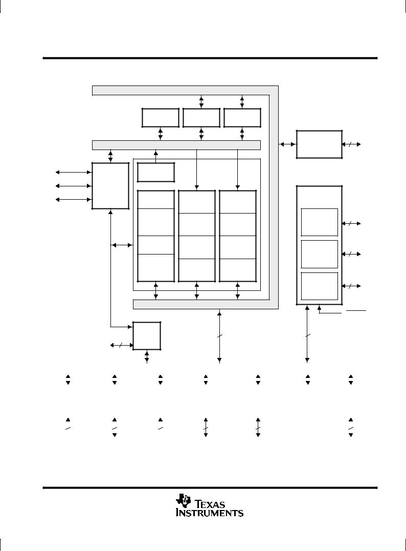
TMS320F243, TMS320F241
DSP CONTROLLERS
SPRS064B ± DECEMBER 1997 ± REVISED FEBRUARY 1999
functional block diagram of the '24x DSP controller
Data Bus
|
Flash |
DARAM |
DARAM |
|
|
|
EEPROM |
B0 |
B1/B2 |
|
|
|
Program Bus |
|
|
Test/ |
7 |
|
|
|
|
||
|
|
|
|
Emulation |
|
Memory² |
|
|
'C2xx |
|
|
Control |
|
|
|
|
|
Instruction |
|
CPU |
|
|
|
|
|
|
|
||
Interrupts |
Register |
|
|
|
|
Program |
|
|
|
|
|
|
|
|
|
|
|
Initialization |
Controller |
|
|
Event |
|
|
Input |
|
|
||
|
|
Manager |
|
||
|
ARAU |
Multiplier |
|
||
|
Shifter |
|
|||
|
|
|
|||
|
|
|
|
|
|
|
Status/ |
|
|
General- |
2 |
|
Control |
ALU |
TREG |
Purpose |
|
|
|
||||
|
Registers |
Timers |
|
||
|
|
|
|
||
|
Auxiliary |
Accumulator |
PREG |
|
|
|
Registers |
Compare |
8 |
||
|
|
|
|||
|
|
|
|
|
|
|
Memory |
|
|
Units |
|
|
|
|
|
|
|
|
Mapped |
Output |
Product |
|
|
|
Registers |
Shifter |
Shifter |
Capture/ |
|
|
|
|
|
3 |
|
|
|
|
|
Quadrature |
|
|
|
|
|
|
|
|
|
|
|
Encoder |
|
|
|
|
|
Pulse (QEP) |
|
PDPINT
|
Clock |
16 |
16 |
2 |
Module |
|
|
|
|
|
Peripheral Bus
|
|
|
|
|
|
|
|
|
|
|
|
|
|
|
|
|
|
|
|
|
|
|
|
|
|
|
|
|
|
|
|
|
|
|
|
|
|
|
|
|
|
|
|
|
|
|
|
General- |
|
Single |
10-Bit |
|
Serial- |
|
Serial- |
|
|
|
|
|
|
|
|||
|
Interrupts |
|
|
Analog- |
|
|
|
Watchdog |
|
|
|
|
|||||||||
|
|
Purpose |
|
|
Peripheral |
|
Communications |
|
|
CAN Module |
|
||||||||||
|
|
|
to-Digital |
|
|
|
Timer |
|
|
||||||||||||
|
Resets |
|
I/O Pins |
|
|
Interface |
|
Interface |
|
|
|
|
|
||||||||
|
|
|
|
|
Converter |
|
|
|
|
|
|
|
|
|
|||||||
|
|
|
|
|
|
|
|
|
|
|
|
|
|
|
|
|
|
|
|
||
|
|
|
|
|
|
|
|
|
|
|
|
|
|
|
|
|
|
|
|
|
|
|
|
4 |
|
|
32³ |
|
|
8 |
|
4 |
|
2 |
|
|
|
|
|
2 |
|
||
|
|
|
|
|
|
|
|
|
|
|
|
|
|
||||||||
² 'F243 only ³ 26 in 'F241
POST OFFICE BOX 1443 •HOUSTON, TEXAS 77251±1443 |
17 |

TMS320F243, TMS320F241
DSP CONTROLLERS
SPRS064B ± DECEMBER 1997 ± REVISED FEBRUARY 1999
architectural overview
The functional block diagram provides a high-level description of each component in the 'F243/'F241 DSP controllers. The TMS320x24x devices are composed of three main functional units: a 'C2xx DSP core, internal memory, and peripherals. In addition to these three functional units, there are several system-level features of the 'F243/'F241 that are distributed. These system features include the memory map, device reset, interrupts, digital input/output (I/O), clock generation, and low-power operation.
system-level functions
device memory maps
The 'F243/'F241 devices implement three separate address spaces for program memory, data memory, and I/O space. On the 'F243/'F241, the first 96 (0±5Fh) data memory locations are either allocated for memory-mapped registers or reserved. This memory-mapped register space contains various control and status registers, including those for the CPU.
All the on-chip peripherals of the 'F243/'F241 devices are mapped into data memory space. Access to these registers is made by the CPU instructions addressing their data memory locations. Figure 1 shows the 'F243 memory map and Figure 2 shows the 'F241 memory map.
18 |
POST OFFICE BOX 1443 •HOUSTON, TEXAS 77251±1443 |
TMS320F243, TMS320F241
DSP CONTROLLERS
SPRS064B ± DECEMBER 1997 ± REVISED FEBRUARY 1999
memory maps
Hex 0000
002F
0030
1FFF
2000
FDFF FE00
FEFF FF00
FFFF
Program
Interrupts
Unused
External
Reserved²
(CNF = 1)
External (CNF = 0)
On-Chip DARAM
(B0)² (CNF = 1)
External (CNF = 0)
Hex 0000
005F
0060
007F
0080
01FF
0200
02FF
0300
03FF
0400
6FFF
7000
73FF
7400
743F
7440
7FFF
8000
FFFF
Data
Memory-Mapped
Registers/Reserved
Addresses
On-Chip
DARAM B2
Reserved/
Illegal
On-Chip DARAM
(B0)³ (CNF = 0)
Reserved (CNF = 1)
On-Chip
DARAM (B1)§
Reserved/
Illegal
Peripheral Memory-
Mapped Registers
(System,WD, ADC,
SCI, SPI, CAN, I/O,
Interrupts)
Peripheral
Memory-Mapped
Registers
(Event Manager)
Illegal
External
Hex |
I/O |
0000 |
|
External
FEFF
FF00
|
|
Reserved/ |
||
|
|
Illegal |
||
FF0E |
|
|
|
|
FF0F |
Flash Control |
|||
|
|
Mode Register |
||
FF10 |
|
|
||
Reserved |
||||
|
|
|||
FFFE |
|
|
||
FFFF |
Wait-State Generator |
|||
Control Register |
||||
|
|
(On-Chip) |
||
On-Chip FLASH memory, (8K) ± if MP/MC = 0
External Program Memory ± if MP/MC = 1
²When CNF = 1, addresses FE00h±FEFFh and FF00h±FFFFh are mapped to the same physical block (B0) in program-memory space. For example, a write to FE00h will have the same effect as a write to FF00h. For simplicity, addresses FE00h±FEFFh are referred to as reserved
when CNF = 1.
³When CNF = 0, addresses 0100h±01FFh and 0200h±02FFh are mapped to the same physical block (B0) in data-memory space. For example, a write to 0100h will have the same effect as a write to 0200h. For simplicity, addresses 0100h±01FFh are referred to as reserved.
§Addresses 0300h±03FFh and 0400h±04FFh are mapped to the same physical block (B1) in data-memory space. For example, a write to 0400h has the same effect as a write to 0300h. For simplicity, addresses 0400h±04FFh are referred to as reserved.
Figure 1. TMS320F243 Memory Map
POST OFFICE BOX 1443 •HOUSTON, TEXAS 77251±1443 |
19 |
TMS320F243, TMS320F241
DSP CONTROLLERS
SPRS064B ± DECEMBER 1997 ± REVISED FEBRUARY 1999
memory maps (continued)
Hex 0000
002F
0030
1FFF
2000
FDFF FE00
FEFF FF00
FFFF
Program
Interrupts
Unused
Reserved
Reserved²
(CNF = 1)
External (CNF = 0)
On-Chip DARAM
B0² (CNF = 1)
External (CNF = 0)
Hex 0000
005F
0060
007F
0080
01FF
0200
02FF
0300
03FF
0400
6FFF
7000
73FF
7400
743F
7440
7FFF
8000
FFFF
Data
Memory-Mapped
Registers/Reserved
Addresses
On-Chip
DARAM B2
Reserved/
Illegal
On-Chip DARAM
(B0)³ (CNF = 0)
Reserved (CNF = 1)
On-Chip
DARAM (B1)§
Reserved/
Illegal
Peripheral Memory-
Mapped Registers
(System,WD, ADC,
SCI, SPI, CAN, I/O,
Interrupts)
Peripheral
Memory-Mapped
Registers
(Event Manager)
Illegal
Reserved
Hex 0000
FF0E
FF0F
FF10
FFFF
I/O
Reserved
Flash Control
Mode Register
Reserved
On-Chip FLASH memory, (8K) ± if MP/MC = 0
External Program Memory ± if MP/MC = 1
²When CNF = 1, addresses FE00h±FEFFh and FF00h±FFFFh are mapped to the same physical block (B0) in program-memory space. For example, a write to FE00h will have the same effect as a write to FF00h. For simplicity, addresses FE00h±FEFFh are referred to as reserved when CNF = 1.
³When CNF = 0, addresses 0100h±01FFh and 0200h±02FFh are mapped to the same physical block (B0) in data-memory space. For example, a write to 0100h will have the same effect as a write to 0200h. For simplicity, addresses 0100h±01FFh are referred to as reserved.
§Addresses 0300h±03FFh and 0400h±04FFh are mapped to the same physical block (B1) in data-memory space. For example, a write to 0400h has the same effect as a write to 0300h. For simplicity, addresses 0400h±04FFh are referred to as reserved.
NOTE A: There is no external memory space for program, data, or I/O in the 'F241.
Figure 2. TMS320F241 Memory Map
20 |
POST OFFICE BOX 1443 •HOUSTON, TEXAS 77251±1443 |
TMS320F243, TMS320F241
DSP CONTROLLERS
SPRS064B ± DECEMBER 1997 ± REVISED FEBRUARY 1999
peripheral memory map
The system and peripheral control register frame contains all the data, status, and control bits to operate the system and peripheral modules on the device (excluding the event manager). The register frame is mapped in the data memory space.
Hex
0000
005F
0060
007F
0080
01FF
0200
02FF
0300
03FF
0400
07FF
0800
6FFF
7000
73FF
7400
743F
7440
77FF
7800
7FFF
8000
FFFF
Memory-Mapped Registers
and Reserved
On-Chip DARAM B2
Reserved
On-Chip DARAM B0
On-Chip DARAM B1
Reserved
Illegal
Peripheral Frame 1 (PF1)
Peripheral Frame 2 (PF2)
Reserved
Illegal
External²
Reserved
Interrupt-Mask Register
Global-Memory Allocation
Register
Interrupt Flag Register
Emulation Registers
and Reserved
Illegal
System Configuration and
Control Registers
Watchdog Timer Registers
ADC Control Registers
SPI
SCI
Illegal
External-Interrupt Registers
Illegal
Digital-I/O Control Registers
Illegal
CAN Control Registers
Illegal
General-Purpose
Timer Registers
Compare, PWM, and
Deadband Registers
Capture & QEP Registers
Interrupt Mask, Vector and
Flag Registers
Reserved
² Reserved in the 'F241
Figure 3. Peripheral Memory Map for 'F243/'F241
Hex
0000
0003
0004
0005
0006
0007
005F
7000 ± 700F
7010 ± 701F
7020 ± 702F
7030 ± 703F
7040 ± 704F
7050 ± 705F
7060 ± 706F
7070 ± 707F
7080 ± 708F
7090 ± 709F 70A0±70FF 7100±722F 7230±73FF
7400 ± 7408
7411 ± 7419
7420 ± 7429
742C ± 7431
7432 ± 743F
POST OFFICE BOX 1443 •HOUSTON, TEXAS 77251±1443 |
21 |

TMS320F243, TMS320F241
DSP CONTROLLERS
SPRS064B ± DECEMBER 1997 ± REVISED FEBRUARY 1999
software-controlled wait-state generator
Due to the fast cycle time of the 'F243 devices, it is often necessary to operate with wait states to interface with external logic or memory. For many systems, one wait state is adequate.
The software wait-state generator can be programmed to generate between 0 and 7 wait states for a given space. Software wait states are configured through the wait-state generator register (WSGR). The WSGR includes three 3-bit fields to configure wait states for the following external memory spaces: data space (DSWS), program space (PSWS), and I/O space (ISWS). The wait-state generator enables wait states for a given memory space based on the value of the corresponding three bits, regardless of the condition of the READY signal. The READY signal can be used to generate additional wait states. All bits of the WSGR are set to 1 at reset so that the device can operate from slow memory at reset. The WSGR register (shown in Table 3, Table 4 and Table 5) resides at I/O location FFFFh. This register should not be accessed in the 'F241.
Table 3. Wait-State Generator Control Register (WSGR)
15 |
12 |
11 |
10 |
9 |
8 |
6 |
5 |
3 |
2 |
0 |
Reserved |
|
|
|
BVIS |
ISWS |
|
DSWS |
|
|
PSWS |
|
|
|
|
|
|
|
|
|
|
|
0 |
|
|
R/W±11 |
R/W±111 |
|
R/W±111 |
|
|
R/W±111 |
|
LEGEND: |
|
|
|
|
|
|
|
|
|
|
0 = Always read as zeros, R = Read Access, W= Write Access, ± n = Value after reset
Table 4. Wait-State(s) Programming
PSWS, DSWS, ISWS BITS |
WAIT STATES FOR PROGRAM, DATA, OR I / O |
|
|
000 |
0 |
|
|
001 |
1 |
|
|
010 |
2 |
|
|
011 |
3 |
|
|
100 |
4 |
|
|
101 |
5 |
|
|
110 |
6 |
|
|
111 |
7 |
|
|
Table 5. Wait-State Generator Control Register (WSGR) |
|
||
|
|
|
|
|
|
BITS |
NAME |
DESCRIPTION |
|
||
|
|
|
|
|
|
|
|
External program space wait states. PSWS determines that between 0 to 7 wait states are applied to all reads |
|
||
2 ± 0 |
PSWS |
and writes to off-chip program space address. The memory cycle can be further extended by using the READY |
|
||
signal. The READY signal does not override the wait states generated by PSWS. These bits are set to 1 (active) |
|
||||
|
|
|
|||
|
|
by reset (RS). |
|
||
|
|
|
|
|
|
|
|
External data space wait states. DSWS determines that between 0 to 7 wait states are applied to all reads and |
|
||
5 ± 3 |
DSWS |
writes to off-chip data space. The memory cycle can be further extended by using the READY signal. The READY |
|
||
|
|
signal does not override the wait states generated by DSWS. These bits are set to 1 (active) by reset (RS). |
|
||
|
|
|
|
||
|
|
External input / output space wait state. ISWS determines that between 0 to 7 wait states are applied to all reads |
|
||
8 ± 6 |
ISWS |
and writes to off-chip I / O space. The memory cycle can be further extended by using the READY signal. The |
|
||
|
|
READY signal does not override the wait states generated by ISWS. These bits are set to 1 (active) by reset |
(RS) |
. |
|
|
|
|
|
||
|
|
Bus visibility modes. Bits 10 and 9 allow selection of various bus visibility modes while running from internal |
|
||
10± 9 |
BVIS |
program and/or data memory. These modes provide a method of tracing internal bus activity. These bits are set |
|
||
to 11b by reset (RS), causing internal program address and program data to be output on the external address |
|
||||
|
|
|
|||
|
|
and data pins. See Table 6. |
|
||
|
|
|
|
||
15± 11 |
± |
Reserved |
|
||
|
|
|
|
|
|
|
|
|
|
|
|
22 |
POST OFFICE BOX 1443 •HOUSTON, TEXAS 77251±1443 |

|
|
|
TMS320F243, TMS320F241 |
||
|
|
|
DSP CONTROLLERS |
||
|
|
|
SPRS064B ± DECEMBER 1997 ± REVISED FEBRUARY 1999 |
||
|
|
|
|
|
|
software-controlled wait-state generator (continued) |
|||||
|
|
Table 6. Visibility Modes |
|||
|
|
|
|
|
|
|
BIT 10 |
BIT 9 |
VISIBILITY MODE |
|
|
|
|
|
|
|
|
|
0 |
0 |
Bus visibility OFF (reduces power consumption and noise) |
|
|
|
|
|
|
|
|
|
0 |
1 |
Bus visibility OFF (reduces power consumption and noise) |
|
|
|
|
|
|
|
|
|
1 |
0 |
Data-address bus output to external address bus. |
|
|
|
Data-data bus output to external data bus. |
|
|
||
|
|
|
|
||
|
|
|
|
|
|
|
1 |
1 |
Program-address bus output to external address bus. |
|
|
|
Program-data bus output to external data bus. |
|
|
||
|
|
|
|
||
|
|
|
|
|
|
digital I/O and shared pin functions
The 'F243 has a total of 32 general-purpose, bidirectional, digital I/O (GPIO) pins that function as follows: six pins are dedicated I/O pins (see Table 7) and 26 pins are shared between primary functions and I/O. The 'F241 has 26 I/O pins; all are shared with other functions. The digital I/O ports module provides a flexible method for controlling both dedicated I/O and shared pin functions. All I/O and shared pin functions are controlled using eight 16-bit registers. These registers are divided into two types:
DOutput Control Registers Ð used to control the multiplexer selection that chooses between the primary function of a pin or the general-purpose I/O function.
DData and Control Registers Ð used to control the data and data direction of bidirectional I/O pins.
Table 7. Dedicated I/O Pins ('F243 Only)
'F243 PIN NUMBER |
PIN NAME |
|
|
20 |
IOPD2 |
|
|
21 |
IOPD3 |
|
|
23 |
IOPD4 |
|
|
25 |
IOPD5 |
|
|
27 |
IOPD6 |
|
|
29 |
IOPD7 |
description of shared I/O pins
The control structure for shared I/O pins is shown in Figure 4, where each pin has three bits that define its operation:
DMux control bit Ð this bit selects between the primary function (1) and I/O function (0) of the pin.
DI/O direction bit Ð if the I/O function is selected for the pin (mux control bit is set to 0), this bit determines whether the pin is an input (0) or an output (1).
DI/O data bit Ð if the I/O function is selected for the pin (mux control bit is set to 0) and the direction selected is an input, data is read from this bit; if the direction selected is an output, data is written to this bit.
The mux control bit, I/O direction bit, and I/O data bit are in the I/O control registers.
POST OFFICE BOX 1443 •HOUSTON, TEXAS 77251±1443 |
23 |
TMS320F243, TMS320F241
DSP CONTROLLERS
SPRS064B ± DECEMBER 1997 ± REVISED FEBRUARY 1999
description of shared I/O pins (continued)
IOP Data Bit |
Primary |
(Read/Write) |
|
|
Function |
IOP DIR Bit
0 = Input
1 = Output
In |
Out |
Note: When the MUX control bit = 1, the primary function is selected in all cases except for the following pins:
1. XF/IOPC0 (0 = Primary Function)
2. BIO/IOPC1 (0 = Primary Function)
3. CLKOUT/IOPD0 (0 = Primary Function)
0 |
1 |
MUX Control Bit |
|
|
0 = I/O Function |
|
|
1 = Primary Function |
Primary Function Pin or I/O Pin
Figure 4. Shared Pin Configuration
A summary of shared pin configurations and associated bits is shown in Table 8.
24 |
POST OFFICE BOX 1443 •HOUSTON, TEXAS 77251±1443 |

|
|
|
|
|
|
|
|
|
|
TMS320F243, TMS320F241 |
|||
|
|
|
|
|
|
|
|
|
|
|
DSP CONTROLLERS |
||
|
|
|
|
|
|
|
|
SPRS064B ± DECEMBER 1997 ± REVISED FEBRUARY 1999 |
|||||
|
|
|
|
|
|
|
|
|
|
|
|
|
|
description of shared I/O pins (continued) |
|
|
|
|
|
|
|
|
|||||
|
|
|
|
Table 8. Shared Pin Configurations |
|
|
|
|
|||||
|
|
|
|
|
|
|
|
|
|
|
|||
|
PIN # |
|
MUX CONTROL |
|
PIN FUNCTION SELECTED |
|
I/O PORT DATA AND DIRECTION² |
|
|||||
144 |
68 |
64 |
REGISTER |
|
(OCRx.n = 1) |
(OCRx.n = 0) |
|
REGISTER |
DATA BIT #³ |
DIR BIT #§ |
|
||
PQFP |
PLCC |
QFP |
(name.bit #) |
|
|
|
|||||||
|
|
|
|
|
|
|
|
|
|
||||
|
|
|
|
|
|
|
|
|
|
|
|
|
|
'F243 |
'F241 |
|
|
|
|
|
|
|
|
|
|
|
|
|
|
|
|
|
|
|
|
|
|
|
|
|
|
56 |
54 |
43 |
OCRA.0 |
|
SCITXD |
IOPA0 |
|
PADATDIR |
0 |
8 |
|
||
|
|
|
|
|
|
|
|
|
|
|
|
|
|
58 |
55 |
44 |
OCRA.1 |
|
SCIRXD |
IOPA1 |
|
PADATDIR |
1 |
9 |
|
||
|
|
|
|
|
|
|
|
|
|
|
|
|
|
83 |
66 |
55 |
OCRA.2 |
|
XINT1 |
IOPA2 |
|
PADATDIR |
2 |
10 |
|
||
|
|
|
|
|
|
|
|
|
|
|
|
|
|
123 |
15 |
8 |
OCRA.3 |
|
CAP1/QEP0 |
IOPA3 |
|
PADATDIR |
3 |
11 |
|
||
|
|
|
|
|
|
|
|
|
|
|
|
|
|
121 |
14 |
7 |
OCRA.4 |
|
CAP2/QEP1 |
IOPA4 |
|
PADATDIR |
4 |
12 |
|
||
|
|
|
|
|
|
|
|
|
|
|
|
|
|
119 |
13 |
6 |
OCRA.5 |
|
CAP3 |
IOPA5 |
|
PADATDIR |
5 |
13 |
|
||
|
|
|
|
|
|
|
|
|
|
|
|
|
|
102 |
7 |
64 |
OCRA.6 |
|
PWM1 |
IOPA6 |
|
PADATDIR |
6 |
14 |
|
||
|
|
|
|
|
|
|
|
|
|
|
|
|
|
100 |
6 |
63 |
OCRA.7 |
|
PWM2 |
IOPA7 |
|
PADATDIR |
7 |
15 |
|
||
|
|
|
|
|
|
|
|
|
|
|
|
|
|
|
|
|
|
|
|
|
|
|
|
|
|
|
|
98 |
5 |
62 |
OCRA.8 |
|
PWM3 |
IOPB0 |
|
PBDATDIR |
0 |
8 |
|
||
|
|
|
|
|
|
|
|
|
|
|
|
|
|
96 |
4 |
61 |
OCRA.9 |
|
PWM4 |
IOPB1 |
|
PBDATDIR |
1 |
9 |
|
||
|
|
|
|
|
|
|
|
|
|
|
|
|
|
94 |
3 |
60 |
OCRA.10 |
|
PWM5 |
IOPB2 |
|
PBDATDIR |
2 |
10 |
|
||
|
|
|
|
|
|
|
|
|
|
|
|
|
|
91 |
2 |
59 |
OCRA.11 |
|
PWM6 |
IOPB3 |
|
PBDATDIR |
3 |
11 |
|
||
|
|
|
|
|
|
|
|
|
|
|
|
|
|
130 |
19 |
12 |
OCRA.12 |
|
T1PWM/T1CMP |
IOPB4 |
|
PBDATDIR |
4 |
12 |
|
||
|
|
|
|
|
|
|
|
|
|
|
|
|
|
128 |
18 |
11 |
OCRA.13 |
|
T2PWM/T2CMP |
IOPB5 |
|
PBDATDIR |
5 |
13 |
|
||
|
|
|
|
|
|
|
|
|
|
|
|
|
|
85 |
67 |
56 |
OCRA.14 |
|
TDIR |
IOPB6 |
|
PBDATDIR |
6 |
14 |
|
||
|
|
|
|
|
|
|
|
|
|
|
|
|
|
87 |
68 |
57 |
OCRA.15 |
|
TCLKIN |
IOPB7 |
|
PBDATDIR |
7 |
15 |
|
||
|
|
|
|
|
|
|
|
|
|
|
|
|
|
|
|
|
|
|
|
|
|
|
|
|
|
|
|
49 |
50 |
39 |
OCRB.0 |
|
IOPC0 |
|
XF |
|
PCDATDIR |
0 |
8 |
|
|
|
|
|
|
|
|
|
|
|
|
|
|
|
|
55 |
53 |
42 |
OCRB.1 |
|
IOPC1 |
|
|
|
|
PCDATDIR |
1 |
9 |
|
|
|
BIO |
|
|
|
||||||||
|
|
|
|
|
|
|
|
|
|
|
|
||
60 |
56 |
45 |
OCRB.2 |
|
SPISIMO |
IOPC2 |
|
PCDATDIR |
2 |
10 |
|
||
|
|
|
|
|
|
|
|
|
|
|
|
||
62 |
57 |
46 |
OCRB.3 |
|
SPISOMI |
IOPC3 |
|
PCDATDIR |
3 |
11 |
|
||
|
|
|
|
|
|
|
|
|
|
|
|
||
64 |
58 |
47 |
OCRB.4 |
|
SPICLK |
IOPC4 |
|
PCDATDIR |
4 |
12 |
|
||
|
|
|
|
|
|
|
|
|
|
|
|
||
66 |
59 |
48 |
OCRB.5 |
|
SPISTE |
IOPC5 |
|
PCDATDIR |
5 |
13 |
|
||
|
|
|
|
|
|
|
|
|
|
|
|
||
115 |
11 |
4 |
OCRB.6 |
|
CANTX |
IOPC6 |
|
PCDATDIR |
6 |
14 |
|
||
|
|
|
|
|
|
|
|
|
|
|
|
||
113 |
10 |
3 |
OCRB.7 |
|
CANRX |
IOPC7 |
|
PCDATDIR |
7 |
15 |
|
||
|
|
|
|
|
|
|
|
|
|
|
|
||
|
|
|
|
|
|
|
|
|
|
|
|
||
116 |
12 |
5 |
OCRB.8 |
|
IOPD0 |
CLKOUT |
|
PDDATDIR |
0 |
8 |
|
||
|
|
|
|
|
|
|
|
|
|
|
|
||
81 |
65 |
54 |
OCRB.9 |
|
XINT2/ADCSOC |
IOPD1 |
|
PDDATDIR |
1 |
9 |
|
||
² Valid only if the I/O function is selected on the pin.
³ If the GPIO pin is configured as an output, these bits can be written to. If the pin is configured as an input, these bits are read from. § If the DIR bit is 0, the GPIO pin functions as an input. For a value of 1, the pin is configured as an output.
NOTE: GPIO pins IOPD2 to IOPD7 are dedicated I/O pins in 'F243. These pins are not available in the 'F241.
POST OFFICE BOX 1443 •HOUSTON, TEXAS 77251±1443 |
25 |

TMS320F243, TMS320F241
DSP CONTROLLERS
SPRS064B ± DECEMBER 1997 ± REVISED FEBRUARY 1999
digital I/O control registers
Table 9 lists the registers available in the digital I/O module. As with other 'F243/'F241 peripherals, the registers are memory-mapped to the data space.
Table 9. Addresses of Digital I/O Control Registers
ADDRESS |
REGISTER |
NAME |
|
|
|
7090h |
OCRA |
I/O mux control register A |
|
|
|
7092h |
OCRB |
I/O mux control register B |
|
|
|
7098h |
PADATDIR |
I/O port A data and direction register |
|
|
|
709Ah |
PBDATDIR |
I/O port B data and direction register |
|
|
|
709Ch |
PCDATDIR |
I/O port C data and direction register |
|
|
|
709Eh |
PDDATDIR |
I/O port D data and direction register |
device reset and interrupts
The TMS320x24x software-programmable interrupt structure supports flexible on-chip and external interrupt configurations to meet real-time interrupt-driven application requirements. The 'F243/'F241 recognizes three types of interrupt sources:
DReset (hardwareor software-initiated) is unarbitrated by the CPU and takes immediate priority over any other executing functions. All maskable interrupts are disabled until the reset service routine enables them.
The 'F243/'F241 devices have two sources of reset: an external reset pin and a watchdog timer timeout (reset).
DHardware-generated interrupts are requested by external pins or by on-chip peripherals. There are two types:
±External interrupts are generated by one of four external pins corresponding to the interrupts XINT1, XINT2, PDPINT, and NMI. The first three can be masked both by dedicated enable bits and by the CPU's interrupt mask register (IMR), which can mask each maskable interrupt line at the DSP core. NMI, which is not maskable, takes priority over peripheral interrupts and software-generated interrupts. It can be locked out only by an already executing NMI or a reset.
±Peripheral interrupts are initiated internally by these on-chip peripheral modules: the event manager, SPI, SCI, WD, CAN, and ADC. They can be masked both by enable bits for each event in each peripheral and by the CPU's IMR, which can mask each maskable interrupt line at the DSP core.
DSoftware-generated interrupts for the 'F243/'F241 devices include:
±The INTR instruction. This instruction allows initialization of any 'F243/'F241 interrupt with software. Its operand indicates the interrupt vector location to which the CPU branches. This instruction globally disables maskable interrupts (sets the INTM bit to 1).
±The NMI instruction. This instruction forces a branch to interrupt vector location 24h, the same location used for the nonmaskable hardware interrupt NMI. NMI can be initiated by driving the NMI pin low or by executing an NMI instruction. This instruction globally disables maskable interrupts.
±The TRAP instruction. This instruction forces the CPU to branch to interrupt vector location 22h. The TRAP instruction does not disable maskable interrupts (INTM is not set to 1); therefore, when the CPU branches to the interrupt service routine, that routine can be interrupted by the maskable hardware interrupts.
±An emulator trap. This interrupt can be generated with either an INTR instruction or a TRAP instruction.
26 |
POST OFFICE BOX 1443 •HOUSTON, TEXAS 77251±1443 |

TMS320F243, TMS320F241
DSP CONTROLLERS
SPRS064B ± DECEMBER 1997 ± REVISED FEBRUARY 1999
reset
The reset operation ensures an orderly startup sequence for the device. There are two possible causes of a reset, as shown in Figure 5.
|
Reset |
Watchdog Timer Reset |
Signal |
External Reset (RS) Pin Active |
System Reset |
|
Figure 5. Reset Signals
The two possible reset signals are generated as follows:
DWatchdog timer reset. A watchdog-timer-generated reset occurs if the watchdog timer overflows or an improper value is written to either the watchdog key register or the watchdog control register. (Note that when the device is powered on, the watchdog timer is automatically active.) The watchdog timer reset is reflected on the external RS pin also.
DReset pin active. To generate an external reset pulse on the RS pin, a low-level pulse duration of at least one CPUCLK cycle is necessary to ensure that the device recognizes the reset signal.
Once watchdog reset is activated, the external RS pin is driven (active) low for a minimum of eight CPUCLK cycles. This allows the TMS320x24x device to reset external system components.
The occurrence of a reset condition causes the TMS320x24x to terminate program execution and affects various registers and status bits. During a reset, RAM contents remain unchanged, and all control bits that are affected by a reset are initialized to their reset state.
hardware-generated interrupts
The '24x CPU supports one nonmaskable interrupt (NMI) and six maskable prioritized interrupt requests. The '24x devices have many peripherals, and each peripheral is capable of generating one or more interrupts in response to many events. The '24x CPU does not have sufficient interrupt requests to handle all these peripheral interrupt requests; therefore, a centralized interrupt controller is provided to arbitrate the interrupt requests from all the different sources. Throughout this section, refer to Figure 6 .
POST OFFICE BOX 1443 •HOUSTON, TEXAS 77251±1443 |
27 |

TMS320F243, TMS320F241
DSP CONTROLLERS
SPRS064B ± DECEMBER 1997 ± REVISED FEBRUARY 1999
hardware-generated interrupts (continued)
PDPINT |
IRQ |
IMR |
|
Pulse |
|
||
ADCINT |
|
||
Gen |
IFR |
||
XINT1 |
|||
Unit |
|||
|
|||
XINT2 |
Level 1 |
|
|
SPIINT |
|
||
IRQ GEN |
|
||
RXINT |
|
||
|
INT1 |
||
TXINT |
|
||
|
|
||
CANMBINT |
|
|
|
CANERINT |
|
|
|
CMP1INT |
|
INT2 |
|
CMP2INT |
|
|
|
CMP3INT |
Level 2 |
|
|
TPINT1 |
|
||
IRQ GEN |
|
||
TCINT1 |
|
||
|
|
||
TUFINT1 |
|
|
|
TOFINT1 |
|
CPU |
|
|
|
||
TPINT2 |
|
INT3 |
|
TCINT2 |
Level 3 |
||
TUFINT2 |
IRQ GEN |
|
|
|
|
||
TOFINT2 |
|
|
|
CAPINT1 |
Level 4 |
INT4 |
|
CAPINT2 |
|
||
IRQ GEN |
|
||
CAPINT3 |
|
||
|
|
||
SPIINT |
|
|
|
RXINT |
Level 5 |
INT5 |
|
TXINT |
|||
IRQ GEN |
|
||
CANMBINT |
|
||
|
|
||
CANERINT |
|
|
|
ADCINT |
Level 6 |
INT6 |
|
XINT1 |
|
||
IRQ GEN |
|
||
XINT2 |
IACK |
||
|
|||
|
PIVR & logic |
|
|
|
PIRQR# |
|
|
|
PIACK# |
|
|
|
Data |
Addr |
|
|
Bus |
Bus |
Figure 6. Peripheral Interrupt Expansion Block Diagram
interrupt hierarchy
The number of interrupt requests available is expanded by having two levels of hierarchy in the interrupt request system. There are two levels of hierarchy in both the interrupt request/acknowledge hardware and in the interrupt service routine software.
28 |
POST OFFICE BOX 1443 •HOUSTON, TEXAS 77251±1443 |

TMS320F243, TMS320F241
DSP CONTROLLERS
SPRS064B ± DECEMBER 1997 ± REVISED FEBRUARY 1999
interrupt request structure
1.At the lower level of the hierarchy, the peripheral interrupt requests (PIRQs) from several peripherals to the interrupt controller are ORed together to generate a request to the CPU. There is an interrupt flag bit and an interrupt enable bit located in the peripheral for each event that can cause a peripheral interrupt request. There is also one PIRQ for each event. If an interrupt-causing event occurs in a peripheral, and the corresponding interrupt enable bit is set, the interrupt request from the peripheral to the interrupt controller is asserted. This interrupt request simply reflects the status of the peripheral's interrupt flag gated with the interrupt enable bit. When the interrupt flag is cleared, the interrupt request is cleared. Some peripherals have the capability to make either a high-priority or a low-priority interrupt request. If a peripheral has this capability, the value of its interrupt priority bit is transmitted to the interrupt controller. The interrupt request continues to be asserted until it is either automatically cleared by an interrupt acknowledge or cleared by software.
2.At the upper level of the hierarchy, the ORed PIRQs generate interrupt (INT) requests to the CPU. The request to the '24x CPU is a low-going pulse of 2 CPU clock cycles. The Peripheral Interrupt Expansion (PIE) controller generates an INT pulse when any of the PIRQs controlling that INT go active. If any of the PIRQs capable of asserting that CPU interrupt request are still active in the cycle following an interrupt acknowledge for that INT, another INT pulse is generated (an interrupt acknowledge clears the highest-priority pending PIRQ). Which CPU interrupt requests get asserted by which peripheral interrupt requests, and the relative priority of each peripheral interrupt request, is defined in the interrupt controller and is not part of any of the peripherals. This is shown in Table 10.
POST OFFICE BOX 1443 •HOUSTON, TEXAS 77251±1443 |
29 |

TMS320F243, TMS320F241
DSP CONTROLLERS
SPRS064B ± DECEMBER 1997 ± REVISED FEBRUARY 1999
interrupt request structure (continued)
Table 10. 'F243/'F241 Interrupt Source Priority and Vectors
|
|
CPU |
BIT |
PERIPHERAL |
|
|
|
|
|
|
|
|
INTERRUPT |
|
SOURCE |
|
|||||
INTERRUPT |
OVERALL |
POSITION IN |
INTERRUPT |
|
|
|||||
AND |
MASKABLE? |
PERIPHERAL |
DESCRIPTION |
|||||||
NAME |
PRIORITY |
PIRQRx AND |
VECTOR |
|||||||
VECTOR |
|
MODULE |
|
|||||||
|
|
PIACKRx |
(PIV) |
|
|
|||||
|
|
ADDRESS |
|
|
|
|
|
|||
|
|
|
|
|
|
|
|
|
||
|
|
|
|
|
|
|
|
|||
|
|
RSN |
|
|
|
|
|
pin, |
Reset from pin, watchdog |
|
Reset |
1 |
|
N/A |
N |
|
RS |
||||
0000h |
|
Watchdog |
timeout |
|||||||
|
|
|
|
|
||||||
|
|
|
|
|
|
|
|
|
|
|
Reserved |
2 |
± |
|
N/A |
N |
|
CPU |
Emulator Trap |
||
0026h |
|
|
||||||||
|
|
|
|
|
|
|
|
|
||
|
|
|
|
|
|
|
|
|||
NMI |
3 |
NMI |
|
N/A |
N |
Nonmaskable |
Nonmaskable interrupt |
|||
0024h |
|
Interrupt |
||||||||
|
|
|
|
|
|
|||||
|
|
|
|
|
|
|
|
|
|
|
PDPINT |
4 |
|
0.0 |
0020h |
Y |
|
EV |
Power device protection |
||
|
|
interrupt pin |
||||||||
|
|
|
|
|
|
|
|
|
||
|
|
|
|
|
|
|
|
|
|
|
ADCINT |
5 |
|
0.1 |
0004h |
Y |
|
ADC |
ADC interrupt in |
||
|
|
high-priority mode |
||||||||
|
|
|
|
|
|
|
|
|
||
|
|
|
|
|
|
|
|
|||
XINT1 |
6 |
|
0.2 |
0001h |
Y |
External |
External interrupt pins in |
|||
|
Interrupt Logic |
high priority |
||||||||
|
|
|
|
|
|
|||||
|
|
|
|
|
|
|
|
|||
XINT2 |
7 |
INT1 |
0.3 |
0011h |
Y |
External |
External interrupt pins in |
|||
Interrupt Logic |
high priority |
|||||||||
|
|
|
|
|
||||||
|
|
0002h |
|
|
|
|
|
|
|
|
SPIINT |
8 |
|
|
|
|
|
|
|
||
|
|
|
|
|
|
|
|
|||
|
|
|
|
|
|
|
|
|
|
|
RXINT |
9 |
|
0.5 |
0006h |
Y |
|
SCI |
SCI receiver interrupt in |
||
|
|
high-priority mode |
||||||||
|
|
|
|
|
|
|
|
|
||
|
|
|
|
|
|
|
|
|
|
|
TXINT |
10 |
|
0.6 |
0007h |
Y |
|
SCI |
SCI transmitter interrupt in |
||
|
|
high-priority mode |
||||||||
|
|
|
|
|
|
|
|
|
||
|
|
|
|
|
|
|
|
|
|
|
CANMBINT |
11 |
|
|
|
|
|
|
|
|
|
|
|
|
|
|
|
|
|
|
|
|
CANERINT |
12 |
|
|
|
|
|
|
|
|
|
|
|
|
|
|
|
|
|
|
||
CMP1INT |
13 |
|
0.9 |
0021h |
Y |
|
EV |
Compare 1 interrupt |
||
|
|
|
|
|
|
|
|
|
||
CMP2INT |
14 |
|
0.10 |
0022h |
Y |
|
EV |
Compare 2 interrupt |
||
|
|
|
|
|
|
|
|
|
||
CMP3INT |
15 |
|
0.11 |
0023h |
Y |
|
EV |
Compare 3 interrupt |
||
|
|
INT2 |
|
|
|
|
|
|
||
TPINT1 |
16 |
0.12 |
0027h |
Y |
|
EV |
Timer 1 period interrupt |
|||
|
|
0004h |
|
|
|
|
|
|
|
|
TCINT1 |
17 |
0.13 |
0028h |
Y |
|
EV |
Timer 1 PWM interrupt |
|||
|
|
|||||||||
|
|
|
|
|
|
|
|
|
|
|
TUFINT1 |
18 |
|
0.14 |
0029h |
Y |
|
EV |
Timer 1 underflow |
||
|
|
interrupt |
||||||||
|
|
|
|
|
|
|
|
|
||
|
|
|
|
|
|
|
|
|
||
TOFINT1 |
19 |
|
0.15 |
002Ah |
Y |
|
EV |
Timer 1 overflow interrupt |
||
|
|
|
|
|
|
|
|
|
||
TPINT2 |
20 |
|
1.0 |
002Bh |
Y |
|
EV |
Timer 2 period interrupt |
||
|
|
|
|
|
|
|
|
|
||
TCINT2 |
21 |
INT3 |
1.1 |
002Ch |
Y |
|
EV |
Timer 2 PWM interrupt |
||
TUFINT2 |
22 |
0006h |
1.2 |
002Dh |
Y |
|
EV |
Timer 2 underflow |
||
|
|
interrupt |
||||||||
|
|
|
|
|
|
|
|
|
||
|
|
|
|
|
|
|
|
|
||
TOFINT2 |
23 |
|
1.3 |
002Eh |
Y |
|
EV |
Timer 2 overflow interrupt |
||
|
|
|
|
|
|
|
|
|
||
CAPINT1 |
24 |
INT4 |
1.4 |
0033h |
Y |
|
EV |
Capture 1 interrupt |
||
|
|
|
|
|
|
|
|
|
||
CAPINT2 |
25 |
1.5 |
0034h |
Y |
|
EV |
Capture 2 interrupt |
|||
0008h |
|
|||||||||
|
|
|
|
|
|
|
|
|
||
CAPINT3 |
26 |
|
1.6 |
0035h |
Y |
|
EV |
Capture 3 interrupt |
||
30 |
POST OFFICE BOX 1443 •HOUSTON, TEXAS 77251±1443 |
 Loading...