


TPS62220DDC
Table of contents
 Loading...
Texas Instruments TPS62220DDC, TPS62221DDC, TPS62222DDC, TPS62223DDC, TPS62224DDC Schematic [ru]
...
www.ti.com
FEATURES DESCRIPTION
APPLICATIONS
V
I
GND
EN
SW
FB
C3
4.7 Fm
L1
4.7 Hm
C4
10 Fm
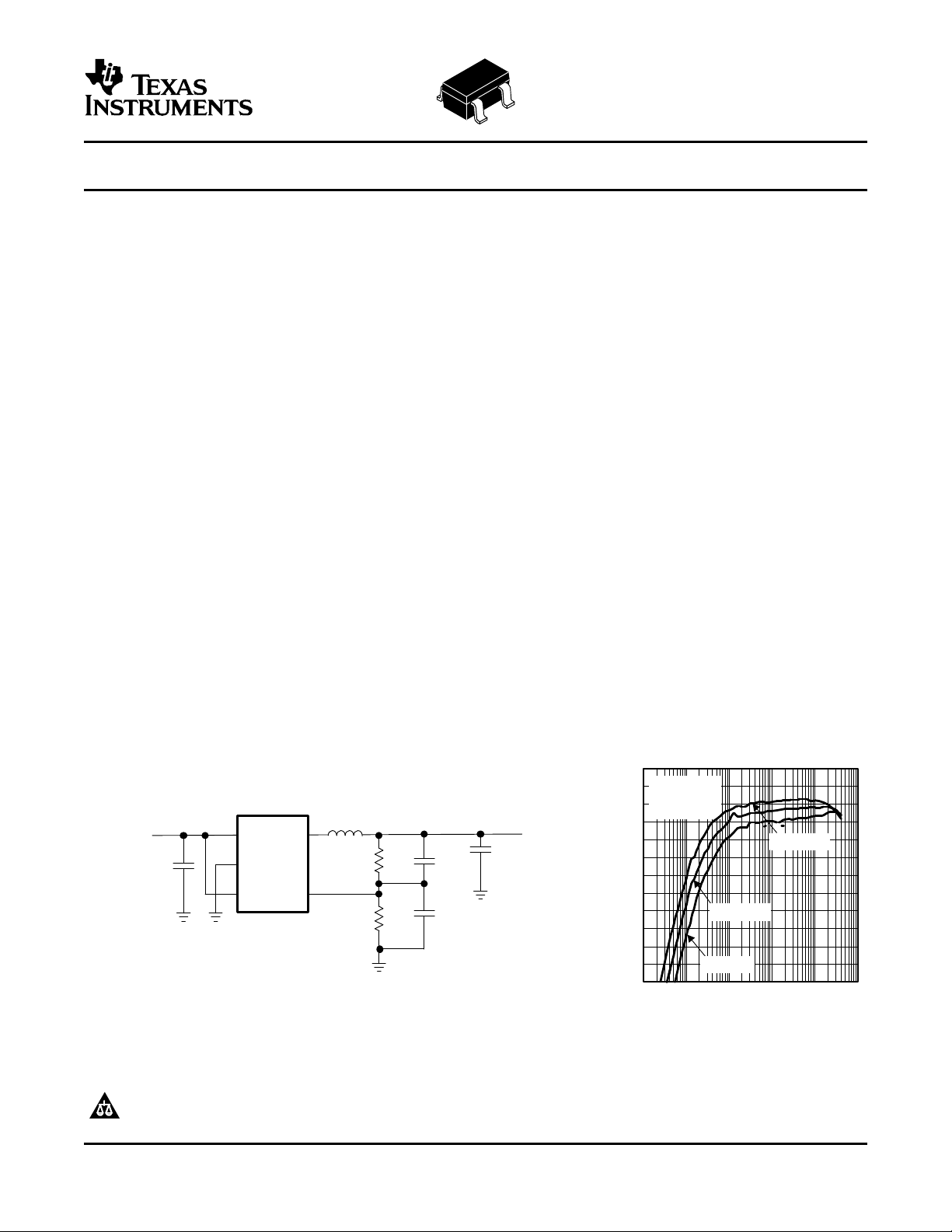
TPS62220
V
I
2.5 V to 6 V
V
O
1.5 V/400 mA
R1
360 kW
R2
180 kW
C1
22 pF
C2
100 pF
1
2
3
5
4
40
45
50
55
60
65
70
75
80
85
90
95
100
0.01 0.1 1 10 100 1000
V
O
= 1.8 V,
L = 4.7 H,m
C
O
= 22 Fm
Efficency − %
I
L
− Load Current − mA
V
I
= 3.7 V
Typical Application (Adjustible Output Voltage Version)
V
I
= 5 V
V
I
= 2.7 V
TPS62220, TPS62221, TPS62222
TPS62223, TPS62224, TPS62227
TPS62228, TPS62229
SLVS491D – SEPTEMBER 2003 – REVISED MARCH 2006
400-mA, 1.25-MHz, HIGH-EFFICIENCY, STEP-DOWN CONVERTER IN THIN-SOT23
• High-Efficiency Synchronous Step-Down
The TPS6222x devices are a family of high-efficiency,
Converter With up to 95% Efficiency
synchronous step-down converters ideally suited for
portable systems powered by 1-cell Li-Ion or 3-cell
• 2.5-V to 6-V Input Voltage Range
NiMH/NiCd batteries. The devices are also suitable to
• Adjustable Output Voltage Range From 0.7 V
operate from a standard 3.3-V or 5-V voltage rail.
to V
I
With an output voltage range of 6 V down to 0.7 V
• Fixed Output Voltage Options Available
and up to 400-mA output current, the devices are
• Up to 400-mA Output Current
ideal for powering the low voltage TMS320™ DSP
• 1.25-MHz Fixed Frequency PWM Operation
family and processors used in PDAs, pocket PCs,
and smart phones. Under nominal load current, the
• Highest Efficiency Over Wide Load Current
devices operate with a fixed switching frequency of
Range Due to Power-Save Mode
typically 1.25 MHz. At light load currents, the part
• 15-µA Typical Quiescent Current
enters the power-save mode operation; the switching
• Soft Start
frequency is reduced and the quiescent current is
typically only 15 µA; therefore, the device achieves
• 100% Duty Cycle Low-Dropout Operation
the highest efficiency over the entire load current
• Dynamic Output-Voltage Positioning
range. The TPS6222x needs only three small
• Available in TSOT23 Package
external components. Together with the tiny TSOT23
package, a minimum system solution size can be
achieved. An advanced fast response voltage mode
control scheme achieves superior line and load
• PDAs and Pocket PC
regulation with small ceramic input and output
• Cellular Phones, Smart Phones
capacitors.
• OMAP™ and Low Power DSP Supply
• Digital Cameras
• Portable Media Players
• Portable Equipment
• WLAN PC Cards
Please be aware that an important notice concerning availability, standard warranty, and use in critical applications of Texas
Instruments semiconductor products and disclaimers thereto appears at the end of this data sheet.
OMAP, TMS320 are trademarks of Texas Instruments.
PRODUCTION DATA information is current as of publication date.
Copyright © 2003–2006, Texas Instruments Incorporated
Products conform to specifications per the terms of the Texas
Instruments standard warranty. Production processing does not
necessarily include testing of all parameters.
www.ti.com
ABSOLUTE MAXIMUM RATINGS
DISSIPATION RATING TABLE
(1)
RECOMMENDED OPERATING CONDITIONS
TPS62220, TPS62221, TPS62222
TPS62223, TPS62224, TPS62227
TPS62228, TPS62229
SLVS491D – SEPTEMBER 2003 – REVISED MARCH 2006
These devices have limited built-in ESD protection. The leads should be shorted together or the device placed in conductive foam
during storage or handling to prevent electrostatic damage to the MOS gates.
ORDERING INFORMATION
(1)
T
A
OUTPUT VOLTAGE THIN-SOT23 PACKAGE SYMBOL
Adjustable TPS62220DDC ALN
1.5 V TPS62221DDC ALO
1.6 V TPS62224DDC ALQ
1.7 V TPS62229DDC EJ
-40°C to 85°C
1.8 V TPS62222DDC APP
1.875 V TPS62228DDC EH
2.3 V TPS62223DDC ALX
1.2 V TPS62227DDC BRZ
(1) The DDC package is available in tape and reel. Add R suffix (TPS62220DDCR) to order quantities of 3000 parts. Add T suffix
(TPS62220DDCT) to order quantities of 250 parts.
over operating free-air temperature (unless otherwise noted)
(1)
TPS6222x UNIT
V
I
Supply voltage on pin
(2)
-0.3 to 7.0 V
Voltages on pins SW, EN, FB
(2)
-0.3 to V
I
+0.3 V
P
D
Continuous power dissipation See Dissipation Rating Table
T
J
Operating junction temperature range -40 to 150 °C
T
stg
Storage temperature -65 to 150 °C
Lead temperature (soldering, 10 sec) 260 °C
(1) Stresses beyond those listed under "absolute maximum ratings” may cause permanent damage to the device. These are stress ratings
only, and functional operation of the device at these or any other conditions beyond those indicated under "recommended operating
conditions” is not implied. Exposure to absolute-maximum-rated conditions for extended periods may affect device reliability.
(2) All voltage values are with respect to network ground terminal.
T
A
≤ 25°C DERATING FACTOR T
A
= 70°C T
A
= 85°C
PACKAGE
POWER RATING ABOVE T
A
= 25°C POWER RATING POWER RATING
DDC 400 mW 4 mW/°C 220 mW 160 mW
(1) The thermal resistance junction to ambient of the 5-pin Thin-SOT23 is 250°C/W.
MIN NOM MAX UNIT
V
I
Supply voltage 2.5 6 V
V
O
Output voltage range for adjustable output voltage version 0.7 V
I
V
I
O
Output current 400 mA
L Inductor
(1)
4.7 µH
C
I
Input capacitor
(1)
4.7 µF
T
A
Operating ambient temperature -40 85 °C
T
J
Operating junction temperature -40 125 °C
(1) See the application section for further information
2
Submit Documentation Feedback
www.ti.com
ELECTRICAL CHARACTERISTICS
TPS62220, TPS62221, TPS62222
TPS62223, TPS62224, TPS62227
TPS62228, TPS62229
SLVS491D – SEPTEMBER 2003 – REVISED MARCH 2006
V
I
= 3.6 V, V
O
= 1.8 V, I
O
= 200 mA, EN = VIN, T
A
= -40 °C to 85 °C, typical values are at T
A
= 25 °C (unless otherwise noted)
PARAMETER TEST CONDITIONS MIN TYP MAX UNIT
SUPPLY CURRENT
V
I
Input voltage range 2.5 6 V
I
Q
Operating quiescent current I
O
= 0 mA, Device is not switching 15 25 µA
Shutdown supply current EN = GND 0.1 1 µA
Undervoltage lockout threshold 1.5 2 V
ENABLE
EN high level input voltage 1.3 V
V
(EN)
EN low level input voltage 0.4 V
I
(EN)
EN input bias current EN = GND or VIN 0.01 0.1 µA
POWER SWITCH
V
I
= V
GS
= 3.6 V 530 670
P-channel MOSFET on-resistance m Ω
V
I
= V
GS
= 2.5 V 670 850
r
DS(on)
V
I
= V
GS
= 3.6 V 430 540
N-channel MOSFET on-resistance m Ω
V
I
= V
GS
= 2.5 V 530 660
P-channel leakage current V
DS
= 6 V 0.1 1 µA
I
lkg
N-channel leakage current V
DS
= 6 V 0.1 1 µA
I
(LIM)
P-channel current limit 2.5 V < V
I
< 6 V 600 670 880 mA
OSCILLATOR
f
S
Switching frequency 0.8 1.25 1.85 MHz
OUTPUT
I
O
Output current 400 mA
Adjustable output voltage
V
O
TPS62220 0.7 V
IN
V
range
V
ref
Reference voltage 0.5 V
V
I
= 3.6 V to 6 V, I
O
= 0 mA 0% 3%
TPS62220
Feedback voltage, See
(1)
Adjustable
V
I
= 3.6 V to 6 V, 0 mA ≤ I
O
≤ 400 mA -3% 3%
V
I
= 2.5 V to 6 V, I
O
= 0 mA 0% 3%
TPS62221
1.5 V
V
I
= 2.5 V to 6 V, 0 mA ≤ I
O
≤ 400 mA -3% 3%
V
I
= 2.5 V to 6 V, I
O
= 0 mA 0% 3%
TPS62224
1.6 V
V
I
= 2.5 V to 6 V, 0 mA ≤ I
O
≤ 400 mA -3% 3%
V
I
= 2.5 V to 6 V, I
O
= 0 mA 0% 3%
TPS62229
1.7 V
V
I
= 2.5 V to 6 V, 0 mA ≤ I
O
≤ 400 mA -3% 3%
V
I
= 2.5 V to 6 V, I
O
= 0 mA 0% 3%
TPS62222
V
O
Fixed output voltage
1.8 V
V
I
= 2.5 V to 6 V, 0 mA ≤ I
O
≤ 400 mA -3% 3%
V
I
= 2.5 V to 6 V, I
O
= 0 mA 0% 3%
TPS62228
1.875 V
V
I
= 2.5 V to 6 V, 0 mA ≤ I
O
≤ 400 mA -3% 3%
V
I
= 2.7 V to 6 V, I
O
= 0 mA 0% 3%
TPS62223
2.3 V
V
I
= 2.7 V to 6 V, 0 mA ≤ I
O
≤ 400 mA -3% 3%
V
I
= 2.7 V to 6 V, I
O
= 0 mA 0% 3%
TPS62227
1.2 V
V
I
= 2.7 V to 6 V, 0 mA ≤ I
O
≤ 400 mA -3% 3%
Line regulation V
I
= 2.5 V to 6 V, I
O
= 10 mA 0.26 %/V
Load regulation I
O
= 100 mA to 400 mA 0.0014 %/mA
Leakage current into SW pin V
I
> V
O
, 0 V ≤ V
(SW)
≤ V
I
0.1 1 µA
I
lkg
Reverse leakage current into pin SW V
I
= open, EN = GND, V
(SW)
= 6 V 0.1 1 µA
(1) For output voltages ≤ 1.2 V, a 22-µF output capacitor value is required to achieve a maximum output voltage accuracy of 3% while
operating in power-save mode (PFM mode). For output voltages ≥ 2 V, an inductor of 10 µH and an output capacitor of ≥ 10 µF is
recommended. See the Application Information section for external components.
3
Submit Documentation Feedback
www.ti.com
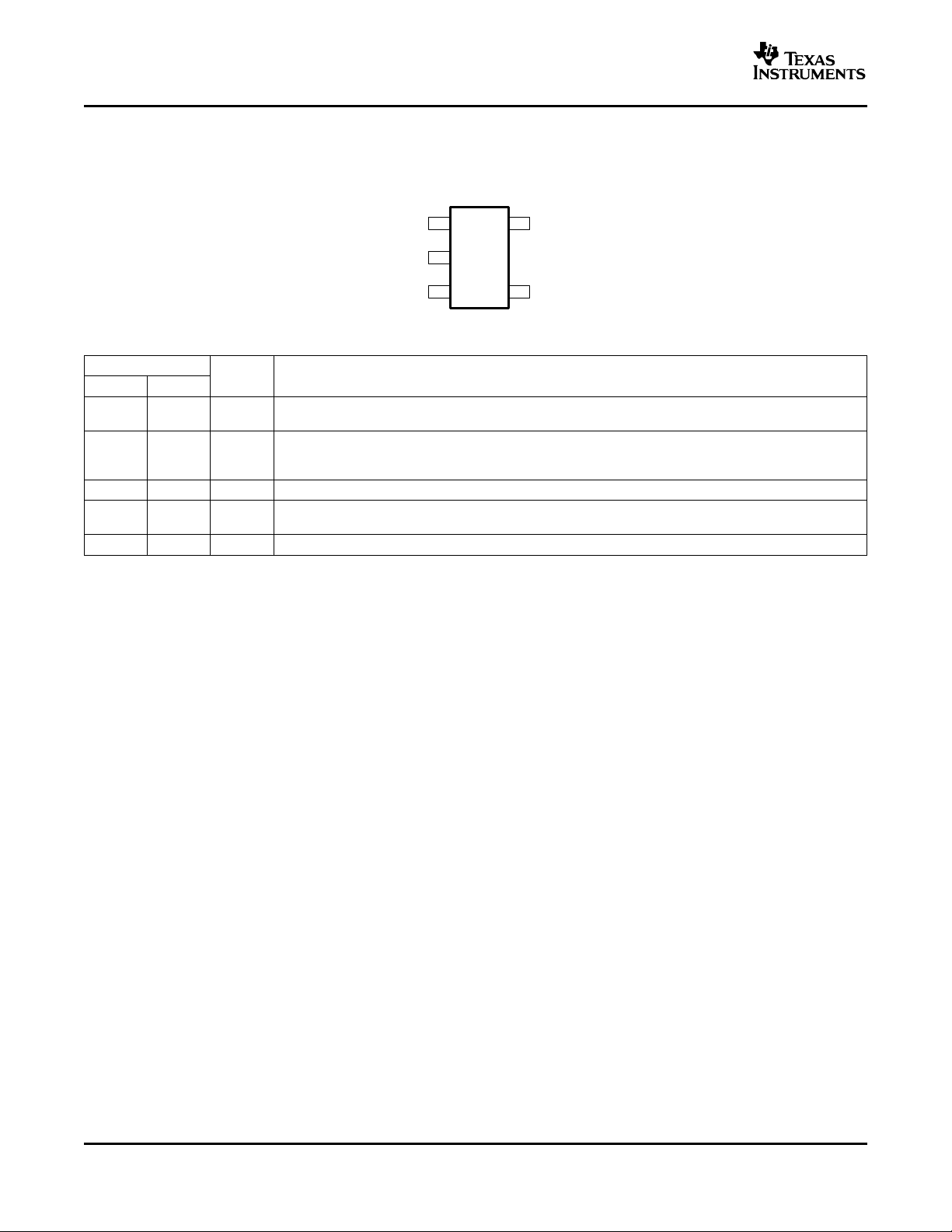
PIN ASSIGNMENTS
3
2
4
5
1
V
I
GND
EN
SW
FB
TPS62220, TPS62221, TPS62222
TPS62223, TPS62224, TPS62227
TPS62228, TPS62229
SLVS491D – SEPTEMBER 2003 – REVISED MARCH 2006
DDC PACKAGE
(TOP VIEW)
Terminal Functions
TERMINAL
I/O DESCRIPTION
NAME NO.
EN 3 I This is the enable pin of the device. Pulling this pin to ground forces the device into shutdown mode.
Pulling this pin to Vin enables the device. This pin must be terminated.
FB 4 I This is the feedback pin of the device. Connect this pin directly to the output if the fixed output voltage
version is used. For the adjustable version, an external resistor divider is connected to this pin. The
internal voltage divider is disabled for the adjustable version.
GND 2 Ground
SW 5 I/O Connect the inductor to this pin. This pin is the switch pin and is connected to the internal MOSFET
switches.
V
I
1 I Supply voltage pin
4
Submit Documentation Feedback
www.ti.com
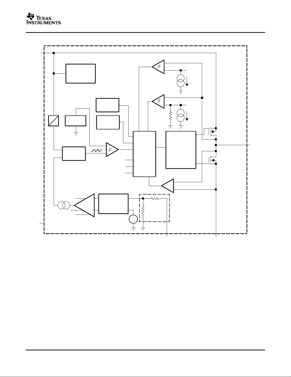
_
+
_
+
_
+
_
+
_
+
REF
REF
Load Comparator
Skip Comparator
Current Limit Comparator
P-Channel
Power MOSFET
Driver
Shoot-Through
Logic
Control
Logic
Soft Start
1.25 MHz
Oscillator
Comparator
S
R
N-Channel
Power MOSFET
Comparator High
Comparator Low
Comparator Low 2
V
(COMP)
Sawtooth
Generator
V
I
Undervoltage
Lockout
Bias Supply
_
+
Comparator High
Comparator Low
Comparator Low 2
Compensation
V
REF
= 0.5 V
R2
See Note
R1
V
I
EN
SW
FB GND
Gm
TPS62220, TPS62221, TPS62222
TPS62223, TPS62224, TPS62227
TPS62228, TPS62229
SLVS491D – SEPTEMBER 2003 – REVISED MARCH 2006
FUNCTIONAL BLOCK DIAGRAM
NOTE: For the adjustable version (TPS62220) the internal feedback divider is disabled, and the FB pin is directly connected
to the internal GM amplifier
5
Submit Documentation Feedback
www.ti.com
TYPICAL CHARACTERISTICS
40
45
50
55
60
65
70
75
80
85
90
95
100
0.01 0.1 1 10 100 1000
V
O
= 3.3 V ,
L = 4.7 µH,
C
O
= 10 µF
V
I
= 3.7 V
V
I
= 5 V
Efficency - %
I
L
- Load Current - mA
40
45
50
55
60
65
70
75
80
85
90
95
100
0.01 0.1 1 10 100 1000
V
O
= 1.8 V ,
L = 4.7 µH,
C
O
= 22 µF
V
I
= 2.7 V
V
I
= 5 V
Efficency - %
I
L
- Load Current - mA
V
I
= 3.7 V
TPS62220, TPS62221, TPS62222
TPS62223, TPS62224, TPS62227
TPS62228, TPS62229
SLVS491D – SEPTEMBER 2003 – REVISED MARCH 2006
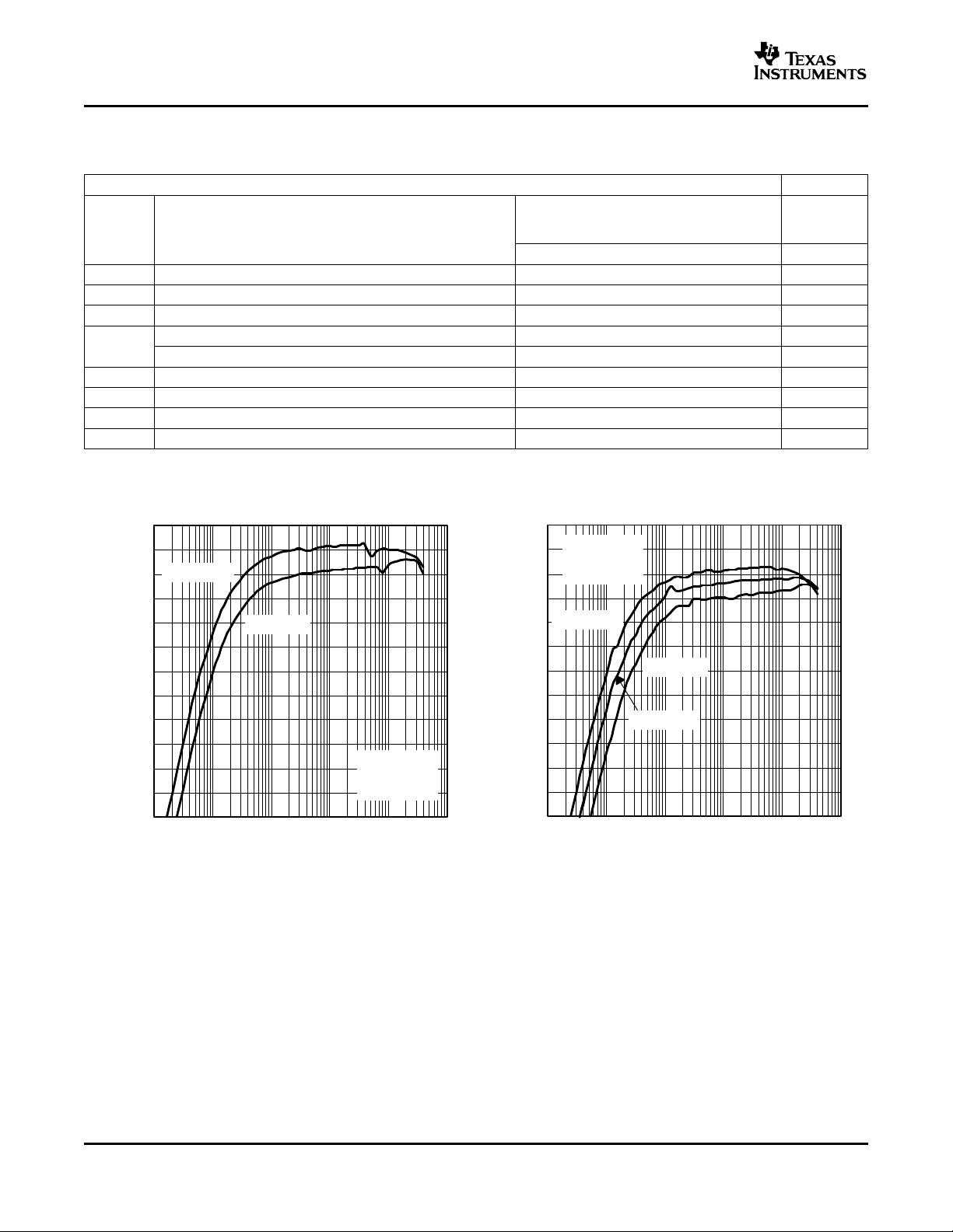
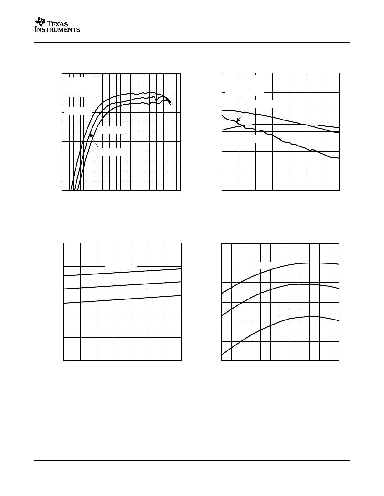
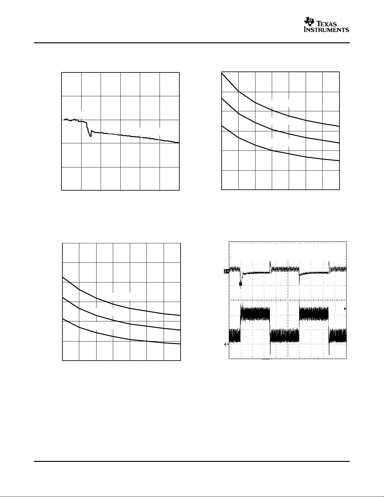
Table of Graphs
FIGURE
Figure 1 ,
vs Load current Figure 2 ,
η Efficiency
Figure 3
vs Input voltage Figure 4
I
Q
No load quiescent current vs Input voltage Figure 5
f
s
Switching frequency vs Temperature Figure 6
V
o
Output voltage vs Output current Figure 7
r
ds(on)
- P-channel switch, vs Input voltage Figure 8
r
ds(on)
r
ds(on)
- N-Channel rectifier switch vs Input voltage Figure 9
Load transient response Figure 10
PWM mode operation Figure 11
Power-save mode operation Figure 12
Start-up Figure 13
EFFICIENCY EFFICIENCY
vs vs
LOAD CURRENT LOAD CURRENT
Figure 1. Figure 2.
6
Submit Documentation Feedback
www.ti.com
70
75
80
85
90
95
100
2.5 3 3.5 4 4.5 5 5.5 6
V
O
= 1.8 V ,
L = 4.7 µH,
C
O
= 22 µF
I
L
= 150 mA
I
L
= 300 mA
Efficiency − %
V
I
− Input Voltage − V
I
L
= 1 mA
40
45
50
55
60
65
70
75
80
85
90
95
100
0.01 0.1 1 10 100 1000
V
O
= 1.5 V ,
L = 4.7 µH,
C
O
= 10 µF
V
I
= 2.7 V
V
I
= 5 V
Efficency - %
I
L
- Load Current - mA
V
I
= 3.7 V
0
5
10
15
20
25
2.5 3 3.5 4 4.5 5 5.5 6
T
A
= 85°C
T
A
= 25°C
T
A
= −40°C
N0 Load Quiescent Current −
V
I
− Input Voltage − V
Aµ
1130
1140
1150
1160
1170
1180
1190
−40 −30 −20 −10 0 10 20 30 40 50 60 70 80
T
A
− Temperature − °C
V
I
= 3.6 V
V
I
= 6 V
V
I
= 2.5 V
f − Switching Frequency − kHz
TPS62220, TPS62221, TPS62222
TPS62223, TPS62224, TPS62227
TPS62228, TPS62229
SLVS491D – SEPTEMBER 2003 – REVISED MARCH 2006
EFFICIENCY EFFICIENCY
vs vs
LOAD CURRENT INPUT VOLTAGE
Figure 3. Figure 4.
NO LOAD QUIESCENT CURRENT SWITCHING FREQUENCY
vs vs
INPUT VOLTAGE TEMPERATURE
Figure 5. Figure 6.
7
Submit Documentation Feedback
www.ti.com
0.2
0.3
0.4
0.5
0.6
0.7
0.8
2.5 3 3.5 4 4.5 5 5.5 6
T
A
= 85°C
T
A
= 25°C
T
A
= -40°C
V
I
- Input Voltage - V
r
ds(on)
Ω- P-Channel Switch -
1.45
1.47
1.49
1.51
1.53
1.55
0 50 100 150 200 250 300
− Outrput Voltage − VV
O
I
O
− Output Current − mA
PFM Mode
PWM Mode
V
O
100 mV/div
I
L
200 mA/div
V
I
= 3.6 V , V
O
= 1.5 V , L = 4.7 µH,
C
O
=10 µF, Load Step 50 mA to 390 mA
transient
200 µs/div
0.2
0.3
0.4
0.5
0.6
0.7
0.8
2.5 3 3.5 4 4.5 5 5.5 6
T
A
= 85°C
T
A
= 25°C
T
A
= −40°C
V
I
− Input Voltage − V
rDS
(on)
ΩN-Channel Switch —
TPS62220, TPS62221, TPS62222
TPS62223, TPS62224, TPS62227
TPS62228, TPS62229
SLVS491D – SEPTEMBER 2003 – REVISED MARCH 2006
OUTPUT VOLTAGE r
ds(on)
P-CHANNEL SWITCH
vs vs
OUTPUT CURRENT INPUT VOLTAGE
Figure 7. Figure 8.
r
ds(on)
N-CHANNEL SWITCH LOAD TRANSIENT RESPONSE
vs
INPUT VOLTAGE
Figure 9. Figure 10.
8
Submit Documentation Feedback
Loading...