


 Loading...
TPS51640A, TPS59640, TPS59641
www.ti.com |
SLUSAQ2 –JANUARY 2012 |
Dual-Channel (3-Phase CPU/1-Phase GPU) SVID, D-CAP+™Step-Down Controller for
IMVP-7 VCORE with Two Integrated Drivers
FEATURES
•Intel IMVP-7 Serial VID (SVID) Compliant
•Supports CPU and GPU Outputs
•CPU Channel 1, 2, or 3 Phase
•Single-Phase GPU Channel
•Full IMVP-7 Mobile Feature Set Including Digital Current Monitor
•8-Bit DAC with 0.250-V to 1.52-V Output Range
•Optimized Efficiency at Light and Heavy Loads
•VCORE Overshoot Reduction (OSR)
•VCORE Undershoot Reduction (USR)
•Accurate, Adjustable Voltage Positioning
•8 Independent Frequency Selections per Channel (CPU/GPU)
•Patent Pending AutoBalance™ Phase
Balancing
•Selectable 8-Level Current Limit
•3-V to 28-V Conversion Voltage Range
•Two Integrated Fast FET Drivers w/Integrated Boost FET
•Internal Driver Bypass Mode for Use with DrMOS Devices
•Small 6 × 6 , 48-Pin, QFN, PowerPAD™
Package
DESCRIPTION
The TPS51640A, TPS59640 and TPS59641 are dual-channel, fully SVID compliant IMVP-7 step-down controllers with two integrated gate drivers. Advanced control features such as D-CAP™+ architecture with overlapping pulse support (undershoot reduction, USR) and overshoot reduction (OSR) provide fast transient response, lowest output capacitance and high efficiency. All of these controllers also support single-phase operation for light loads. The full compliment of IMVP-7 I/O is integrated into the controllers including dual PGOOD signals, ALERT
and VR_HOT. Adjustable control of VCORE slew rate and voltage positioning round out the IMVP-7
features. In addition, the controllers' CPU channel includes two high-current FET gate drivers to drive high-side and low-side N-channel FETs with exceptionally high speed and low switching loss. The TPS51601 or TPS51601A driver is used for the third phase of the CPU and the GPU channel.
The BOOT voltage (VBOOT) on the TPS51640A and TPS59640 is 0 V. The TPS59641 is specifically
designed for a VBOOT level of 1.1 V.
These controllers are packaged in a space saving, thermally enhanced 48-pin QFN. The TPS51640A is rated to operate from –10°C to 105°C. The TPS59640 and TPS59641 are rated to operate from –40°C to 105°C.
APPLICATIONS
•IMVP-7 VCORE Applications for Adapter, Battery, NVDC or 3 V/5 V/12 V rails
SIMPLIFIED APPLICATION
|
3-phase CPU |
Internal |
|
FET Driver |
|
|
Controller |
|
|
TPS51601 |
|
|
|
|
|
|
FET Driver |
|
|
Internal |
|
IMVP-7 |
FET Driver |
Processor |
|
|
SVID Interface |
|
|
|
|
|
|
1-phase GPU |
TPS51601 |
|
Controller |
FET Driver |
|
|
TPS51640 |
CPU Power Stage |
|
VCC_CPU |
|
||
|
|
|
GPU Power Stage |
|
VCC_GFX |
|
||
|
|
UDG-11062 |
|
Please be aware that an important notice concerning availability, standard warranty, and use in critical applications of Texas
Instruments semiconductor products and disclaimers thereto appears at the end of this data sheet.
D-CAP+, PowerPAD, D-CAP are trademarks of Texas Instruments.
PRODUCTION DATA information is current as of publication date. |
Copyright © 2012, Texas Instruments Incorporated |
Products conform to specifications per the terms of the Texas |
|
Instruments standard warranty. Production processing does not |
|
necessarily include testing of all parameters. |
|

TPS51640A, TPS59640, TPS59641
SLUSAQ2 –JANUARY 2012 |
www.ti.com |
These devices have limited built-in ESD protection. The leads should be shorted together or the device placed in conductive foam during storage or handling to prevent electrostatic damage to the MOS gates.
ORDERING INFORMATION(1) (2)
TA |
PACKAGE |
VBOOT |
ORDERABLE |
PINS |
TRANSPORT |
MINIMUM |
ECO PLAN |
|
(V) |
NUMBER |
MEDIA |
QUANTITY |
|||||
|
|
|
|
|
|
|
|
|
–10°C to 105°C |
|
0 |
TPS51640ARSLT |
|
|
250 |
|
|
|
|
|
|
|
|
|||
|
TPS51640ARSLR |
|
|
2500 |
|
|||
|
|
|
|
|
|
|||
|
|
|
|
|
|
|
|
|
|
Plastic Quad Flat |
0 |
TPS59640RSLT |
48 |
Tape-and-reel |
250 |
Green (RoHS and |
|
–40°C to 105°C |
Pack (QFN) |
TPS59640RSLR |
2500 |
no Sb/Br) |
||||
|
|
|
||||||
|
|
|
|
|
|
|
||
|
1.1 |
TPS59641RSLT(3) |
|
|
250 |
|
||
|
|
|
|
|
||||
|
|
TPS59641RSLTR(3) |
|
|
2500 |
|
||
|
|
|
|
|
|
(1)For the most current package and ordering information see the Package Option Addendum at the end of this document, or see the TI web site at www.ti.com.
(2)Package drawings, thermal data, and symbolization are available at www.ti.com/packaging.
(3)Product preview. Not currently available.
ABSOLUTE MAXIMUM RATINGS(1) (2)
over operating free-air temperature range (unless otherwise noted)
|
|
|
|
|
|
|
|
|
|
MIN |
TYP MAX |
UNIT |
|
|
|
|
|
|
|
|
|
|
|
|
|
|
VBAT |
–0.3 |
32 |
|
||||||||
|
CSW1, CSW2 |
–6.0 |
32 |
V |
||||||||
|
CDH1 to CSW1; CDH2 to CSW2; CBST1 to CSW1; CBST2 to CSW2 |
–0.3 |
6.0 |
|
||||||||
Input voltage |
CTHERM, CCOMP, CF-IMAX, GF-IMAX, GCOMP, GTHERM, |
–0.3 |
6.0 |
|
||||||||
V5DRV, V5 |
|
|||||||||||
|
|
|
||||||||||
|
|
|
|
V |
||||||||
|
COCP-I, CCSP1, CCSP2, CCSP3, CCSN1, CCSN2, CCSN3, CVFB, |
–0.3 |
|
|||||||||
|
CGFB, V3R3, VR_ON, VCLK, VDIO, SLEWA, GGFB, GVFB, GCSN, |
3.6 |
|
|||||||||
|
GCSP, GOCP-I, |
|
|
|
||||||||
|
PGND |
–0.3 |
0.3 |
|
||||||||
|
VREF |
–0.3 |
1.8 |
|
||||||||
Output voltage |
CPGOOD, |
|
|
|
|
|
GPGOOD, CIMON, GIMON |
–0.3 |
3.6 |
V |
||
ALERT, |
VR_HOT, |
|||||||||||
|
CPWM3, |
|
|
GPWM, |
|
|
CDL1, CDL2 |
–0.3 |
6.0 |
|
||
|
CSKIP, |
GSKIP, |
|
|||||||||
Electrotatic discharge |
(HBM) QSS 009-105 (JESD22-A114A) |
1.5 |
|
kV |
||||||||
|
|
|
|
|
|
|
|
|
|
|
|
|
(CDM) QSS 009-147 (JESD22-C101B.01) |
500 |
|
V |
|||||||||
|
|
|||||||||||
|
|
|
|
|
|
|
|
|
|
|
|
|
Operating junction temperature, TJ |
|
|
|
|
|
|
|
|
|
-40 |
125 |
°C |
Storage temperature, Tstg |
|
|
|
|
|
|
|
|
|
-55 |
150 |
°C |
(1)Stresses beyond those listed under absolute maximum ratings may cause permanent damage to the device. These are stress ratings only and functional operation of the device at these or any other conditions beyond those indicated under recommended operating conditions is not implied. Exposure to absolute-maximum-rated conditions for extended periods may affect device reliability.
(2)All voltage values are with respect to the network ground terminal unless otherwise noted.
2 |
Submit Documentation Feedback |
Copyright © 2012, Texas Instruments Incorporated |

TPS51640A, TPS59640, TPS59641
www.ti.com SLUSAQ2 –JANUARY 2012
THERMAL INFORMATION
|
|
TPS51640A |
|
|
|
|
TPS59640 |
|
|
|
THERMAL METRIC(1) |
TPS59641 |
UNITS |
|
|
|
RSL |
|
|
|
|
48 PINS |
|
|
θJA |
Junction-to-ambient thermal resistance |
31.7 |
|
|
θJCtop |
Junction-to-case (top) thermal resistance |
19.8 |
|
|
θJB |
Junction-to-board thermal resistance |
7.1 |
°C/W |
|
ψJT |
Junction-to-top characterization parameter |
0.3 |
||
|
||||
ψJB |
Junction-to-board characterization parameter |
7.1 |
|
|
θJCbot |
Junction-to-case (bottom) thermal resistance |
2.1 |
|
(1)For more information about traditional and new thermal metrics, see the IC Package Thermal Metrics application report, SPRA953.
RECOMMENDED OPERATING CONDITIONS
|
|
|
|
|
|
|
|
|
|
MIN |
TYP |
MAX |
UNIT |
|
|
|
|
|
|
|
|
|
|
|
|
|
|
|
VBAT |
|
–0.1 |
|
28 |
|
|||||||
|
CSW1, CSW2 |
|
–3.0 |
|
30 |
|
|||||||
|
CDH1 to CSW1; CDH2 to CSW2; CBST1 to CSW1; CBST2 to |
–0.1 |
|
5.5 |
|
||||||||
|
CSW2 |
|
|
|
|||||||||
|
|
|
|
|
|
||||||||
|
|
|
|
|
|
|
|||||||
|
V5DRV, V5 |
|
4.5 |
|
5.5 |
|
|||||||
|
|
|
|
|
|
|
|||||||
|
V3R3 |
|
3.1 |
|
3.5 |
|
|||||||
|
|
|
|
|
|
|
|||||||
Input voltage |
CCOMP, GCOMP |
|
–0.1 |
|
2.5 |
V |
|||||||
|
CTHERM, GTHERM |
|
0.1 |
|
3.6 |
|
|||||||
|
|
|
|
|
|
|
|||||||
|
CF-IMAX, GF-IMAX, COCP-I, GOCP-I |
|
0.1 |
|
1.7 |
|
|||||||
|
|
|
|
|
|
||||||||
|
CCSP1, CCSP2, CCSP3, CCSN1, CCSN2, CCSN3, CVFB, CGFB, |
–0.1 |
|
1.7 |
|
||||||||
|
GGFB, GVFB, GCSN, GCSP, |
|
|
|
|||||||||
|
|
|
|
|
|
||||||||
|
|
|
|
|
|
|
|||||||
|
VR_ON, VCLK, VDIO, SLEWA, |
|
–0.1 |
|
3.5 |
|
|||||||
|
PGND |
|
–0.1 |
|
0.1 |
|
|||||||
|
VREF |
|
–0.1 |
|
1.72 |
|
|||||||
Output voltage |
CIMON, GIMON |
|
–0.1 |
|
VVREF |
V |
|||||||
|
|
|
|
|
|
|
|
|
–0.1 |
|
|
||
CPGOOD, ALERT, VR_HOT, GPGOOD, |
|
|
VV3R3 |
||||||||||
|
|
|
|
||||||||||
|
CPWM3, CSKIP, GPWM, |
|
|
CDL1, CDL2, |
–0.1 |
|
VV5 |
|
|||||
|
GSKIP, |
|
|
||||||||||
Operating free air temperature, TA |
|
TPS51460A |
–10 |
|
105 |
°C |
|||||||
|
TPS59640,TPS59641 |
–40 |
|
105 |
|||||||||
|
|
|
|
|
|
|
|
|
|
|
|||
Copyright © 2012, Texas Instruments Incorporated |
Submit Documentation Feedback |
3 |

TPS51640A, TPS59640, TPS59641
SLUSAQ2 –JANUARY 2012 www.ti.com
ELECTRICAL CHARACTERISTICS
over recommended free-air temperature range, VV5 = VV5DRV = 5.0 V; VV3R3 = 3.3 V; VxGFB = VPGND = VGND, VxVFB = VCORE (Unless otherwise noted)
|
PARAMETER |
TEST CONDITIONS |
|
MIN |
TYP |
MAX |
UNIT |
||
|
|
|
|
|
|
|
|
|
|
SUPPLY: CURRENTS, UVLO AND POWER-ON RESET |
|
|
|
|
|
|
|
||
|
|
|
|
|
|
|
|||
IV5-4 |
V5 supply current CPU: 3-phase |
IV5+ IV5DRV , VVDAC < VxVFB < (VVDAC + 100 mV), |
|
6.0 |
9.0 |
mA |
|||
active GPU: 1-phase active |
VR_ON = ‘HI’ |
|
|
|
|
||||
|
|
|
|
|
|
|
|
||
IV5-3 |
V5 supply current CPU: 2-phase |
IV5+ IV5DRV, VVDAC < VxVFB < (VVDAC + 100 mV), |
|
5.5 |
|
mA |
|||
active GPU: 1-phase active |
VR_ON = ‘HI’, VCCSP3=3.3 V |
|
|
|
|||||
|
|
|
|
|
|
||||
IV5-2 |
V5 supply current CPU: 1-phase |
IV5+ IV5DRV, VVDAC < VxVFB < (VVDAC + 100 mV), |
|
4.9 |
|
mA |
|||
active GPU: 1-phase active |
VR_ON = ‘HI’, VCCSP3 = VCCSP2= 3.3 V |
|
|
|
|||||
|
|
|
|
|
|
||||
|
V5 supply current CPU: 3-phase |
IV5+ IV5DRV, VVDAC < VxVFB < (VVDAC + 100 mV), |
|
|
|
|
|||
IV5-PS3 |
VR_ON = ‘HI’, SetPS = PS3 |
|
|
|
|
5.1 |
|
mA |
|
|
active GPU: 1-phase active |
(Note: 3-phase CPU goes to 1-phase in PS3) |
|
|
|
|
|||
|
|
|
|
|
|
||||
|
|
|
|
|
|
|
|
|
|
IV5STBY |
V5DRV standby current |
VR_ON = ‘LO’, IV5 + IV5DRV |
|
|
|
|
10 |
20 |
µA |
VUVLOH |
V5 UVLO 'OK' Threshold |
Ramp up, VR_ON=’HI’, |
|
|
|
4.25 |
4.4 |
4.5 |
V |
VUVLOL |
V5 UVLO fault threshold |
Ramp down, VR_ON = ’HI’, |
|
|
|
3.95 |
4.2 |
4.3 |
V |
IV3R3 |
V3R3 supply current |
SVID bus idle, VR_ON = ‘HI’ |
|
|
0.5 |
1.0 |
mA |
||
IV3R3SBY |
V3R3 standby current |
VR_ON = ‘LO’ |
|
|
|
|
|
10 |
µA |
V3UVLOH |
V3R3 UVLO 'OK' threshold |
Ramp up, VR_ON=’HI’, |
|
|
|
2.5 |
2.9 |
3.0 |
V |
V3UVLOL |
V3R3 UVLO fault threshold |
Ramp down, VR_ON = ’HI’, |
|
|
|
2.4 |
2.7 |
2.8 |
V |
REFERENCES: DAC, VREF, VBOOT AND DRVL DISCHARGE FOR BOTH CPU AND GPU |
|
|
|
|
|||||
|
|
|
|
|
|
|
|
|
|
|
|
|
|
|
TPS59640 |
|
0 |
|
V |
VBOOT |
Boot voltage |
|
|
|
TPS51640A |
|
|
||
|
|
|
|
|
|
|
|||
|
|
|
TPS59641 |
|
1.1 |
|
|
||
|
|
|
|
|
|
|
|
||
|
|
|
|
|
|
|
|
|
|
VVIDSTP |
VID step size |
|
|
|
|
|
5 |
|
mV |
|
|
0.25 ≤ VxVFB ≤ 0.995V, |
|
|
TPS51640A |
–5 |
|
5 |
|
|
|
IxPU_CORE = 0 A, 0°C ≤ TA ≤ |
85°C |
|
|
|
|||
|
|
|
|
|
|
|
|
||
VDAC1 |
xVFB tolerance no load active |
0.25 ≤ VxVFB ≤ 0.995V, |
|
|
TPS59640 |
–6 |
|
|
|
|
|
IxPU_CORE = 0 A, |
|
|
|
8.3 |
|
||
|
|
|
|
TPS59641 |
|
|
|||
|
|
–40°C ≤ TA ≤ 105°C |
|
|
|
|
|
|
|
|
|
|
|
|
|
|
|
mV |
|
|
|
1.000V ≤ VxVFB ≤ 1.520 V, |
|
|
TPS51640A |
–0.5% |
|
0.5% |
|
|
|
|
|
|
|
||||
|
|
IxPU_CORE = 0 A, 0°C ≤ TA ≤ |
85°C |
|
|
|
|||
|
|
|
|
|
|
|
|
||
VDAC4 |
xVFB tolerance above 1 V VID |
1.000V ≤ VxVFB ≤ 1.520 V, |
|
|
TPS59640 |
–0.65% |
|
|
|
|
|
IxPU_CORE = 0 A, |
|
|
|
1.0% |
|
||
|
|
|
|
TPS59641 |
|
|
|||
|
|
–40°C ≤ TA ≤ 105°C |
|
|
|
|
|
|
|
VVREF |
VREF Output |
4.5 V ≤ VV5 ≤ 5.5 V, IVREF= 0 A |
|
|
1.70 |
|
V |
||
VVREFSRC |
VREF output source |
0 µA ≤ IVREF ≤ 500 µA |
|
|
|
–4 |
–0.1 |
|
mV |
VVREFSNK |
VREF output sink |
–500 µA ≤ IVREF ≤ 0 µA |
|
|
|
|
0.1 |
4 |
mV |
VDLDQ |
DRVL discharge threshold |
Soft-stop transistor turns on at this point. |
|
200 |
300 |
mV |
|||
VOLTAGE SENSE: xVFB AND xGFB FOR BOTH CPU AND GPU |
|
|
|
|
|
|
|
||
|
|
|
|
|
|
|
|
|
|
IxVFB |
xVFB input bias current |
VxVFB=2 V, VxGFB=0 V |
|
|
|
|
20 |
40 |
µA |
IxGFB |
xGFB input bias current |
VxVFB=2 V, VxGFB=0 V |
|
|
|
-40 |
-20 |
|
µA |
AGAINGND |
xGFB/GND gain |
|
|
|
|
|
1 |
|
V/V |
CURRENT MONITOR |
|
|
|
|
|
|
|
|
|
|
|
|
|
|
|
|
|
|
|
VCiMONLK |
Zero level current output |
Σ∆CS = 0 mV, AIMON = 12 × (1+1.27) |
|
|
35 |
|
mV |
||
VCIMONLO |
Low level current output |
Σ∆CS = 15.6 mV, AIMON = 12 × (1+1.27) |
|
425 |
|
mV |
|||
VCIMONMID |
Mid level current output |
Σ∆CS = 31.1 mV, AIMON = 12 × (1+1.27) |
|
850 |
|
mV |
|||
VCIMONHI |
High level current output |
Σ∆CS = 62.3 mV, AIMON = 12 × (1+1.27) |
|
1700 |
|
mV |
|||
ZERO-CROSSING |
|
|
|
|
|
|
|
|
|
|
|
|
|
|
|
|
|
|
|
VZx |
Inductor zero crossing threshold |
|
|
|
|
|
0 |
|
mV |
voltage |
|
|
|
|
|
|
|||
4 |
Submit Documentation Feedback |
Copyright © 2012, Texas Instruments Incorporated |

TPS51640A, TPS59640, TPS59641
www.ti.com SLUSAQ2 –JANUARY 2012
ELECTRICAL CHARACTERISTICS (continued)
over recommended free-air temperature range, VV5 = VV5DRV = 5.0 V; VV3R3 = 3.3 V; VxGFB = VPGND = VGND, VxVFB = VCORE (Unless otherwise noted)
|
PARAMETER |
TEST CONDITIONS |
|
MIN |
TYP |
MAX |
UNIT |
|
|
|
|
|
|
||||
CURRENT SENSE: OVERCURRENT, ZERO CROSSING, VOLTAGE POSITIONING AND PHASE BALANCING |
|
|
||||||
|
|
|
|
|
|
|
|
|
|
|
|
TPS51640A |
5.1 |
7.0 |
9.7 |
|
|
|
|
RxOCP-I = 20 kΩ |
|
|
|
|
|
|
|
|
TPS59640 |
4.6 |
7.0 |
9.7 |
|
||
|
|
|
TPS59641 |
|
||||
|
|
|
|
|
|
|
||
|
|
|
|
|
|
|
|
|
|
|
|
TPS51640A |
8.1 |
10.0 |
12.6 |
|
|
|
|
RxOCP-I = 24 kΩ |
|
|
|
|
|
|
|
|
TPS59640 |
7.6 |
10.0 |
13.1 |
|
||
|
|
|
TPS59641 |
|
||||
|
|
|
|
|
|
|
||
|
|
|
|
|
|
|
|
|
|
|
|
TPS51640A |
12.1 |
14.0 |
16.7 |
|
|
|
|
RxOCP-I = 30 kΩ |
|
|
|
|
|
|
|
|
TPS59640 |
11.6 |
14.0 |
17.2 |
|
||
|
|
|
TPS59641 |
|
||||
|
|
|
|
|
|
|
||
|
|
|
|
|
|
|
|
|
|
|
|
TPS51640A |
17.1 |
19.0 |
21.7 |
|
|
|
|
RxOCP-I = 39 kΩ |
|
|
|
|
|
|
|
|
TPS59640 |
16.6 |
19.0 |
22.2 |
|
||
|
OCP voltage (valley current |
|
TPS59641 |
|
||||
VOCPP |
|
|
|
|
mV |
|||
limit) |
|
TPS51640A |
23.1 |
25.0 |
27.9 |
|||
|
|
|
||||||
|
|
RxOCP-I = 56 kΩ |
|
|
|
|
|
|
|
|
TPS59640 |
22.6 |
25.0 |
28.4 |
|
||
|
|
|
TPS59641 |
|
||||
|
|
|
|
|
|
|
||
|
|
|
|
|
|
|
|
|
|
|
|
TPS51640A |
29.7 |
32.0 |
35.0 |
|
|
|
|
RxOCP-I = 75 kΩ |
|
|
|
|
|
|
|
|
TPS59640 |
29.2 |
32.0 |
35.5 |
|
||
|
|
|
TPS59641 |
|
||||
|
|
|
|
|
|
|
||
|
|
|
|
|
|
|
|
|
|
|
|
TPS51640A |
37.9 |
40.0 |
43.3 |
|
|
|
|
RxOCP-I = 100 kΩ |
|
|
|
|
|
|
|
|
TPS59640 |
37.4 |
40.0 |
43.8 |
|
||
|
|
|
TPS59641 |
|
||||
|
|
|
|
|
|
|
||
|
|
|
|
|
|
|
|
|
|
|
|
TPS51640A |
46.8 |
49.0 |
52.6 |
|
|
|
|
RxOCP-I = 150 kΩ |
|
|
|
|
|
|
|
|
TPS59640 |
46.2 |
49.0 |
53.1 |
|
||
|
|
|
TPS59641 |
|
||||
|
|
|
|
|
|
|
||
|
|
|
|
|
|
|
|
|
|
|
VIMAX_MIN = 133 mV, value of xIMAX, |
|
|
20 |
|
A |
|
V |
IMAX values both channels |
VIMAX = VREF × IMAX / 255 |
|
|
|
|
|
|
IMAX |
|
|
|
|
|
|
|
|
|
VIMAX_MAX = 653mV, value of xIMAX |
|
|
98 |
|
A |
||
|
|
|
|
|
||||
ICS |
CS pin input bias current |
CSPx and CSNx |
|
–1.0 |
0.2 |
1.0 |
µA |
|
IxVFBDQ |
xVFB input bias current, |
End of soft-stop, xVFB = 100mV |
|
90 |
125 |
180 |
µA |
|
discharge |
|
|||||||
|
|
|
|
|
|
|
||
|
|
|
|
|
|
|
|
|
|
Droop amplifier |
|
TPS51640A |
486 |
497 |
518 |
|
|
GM-DROOP |
xVFB = 1 V |
|
|
|
|
µS |
||
TPS59640 |
|
|
|
|||||
transconductance |
480 |
497 |
518 |
|||||
|
|
TPS59641 |
|
|||||
|
|
|
|
|
|
|
||
|
|
|
|
|
|
|
|
|
IBAL_TOL |
Internal current share tolerance |
(VCSP1 – VCSN1) = (VCSP2 – VCSN2) = |
|
–3% |
|
+3% |
|
|
(VCSP3 – VCSN3) = VOCPP_MIN |
|
|
|
|||||
|
|
|
|
|
|
|
||
ACSINT |
Internal current sense gain |
Gain from CSPx – CSNx to PWM comparator |
11.65 |
12.00 |
12.30 |
V/V |
||
Copyright © 2012, Texas Instruments Incorporated |
Submit Documentation Feedback |
5 |

TPS51640A, TPS59640, TPS59641
SLUSAQ2 –JANUARY 2012 www.ti.com
ELECTRICAL CHARACTERISTICS (continued)
over recommended free-air temperature range, VV5 = VV5DRV = 5.0 V; VV3R3 = 3.3 V; VxGFB = VPGND = VGND, VxVFB = VCORE (Unless otherwise noted)
|
PARAMETER |
TEST CONDITIONS |
|
MIN |
TYP |
MAX |
UNIT |
|
|
|
|
|
|
|
|
TIMERS: SLEW RATE, ISLEW, ADDR, ON-TIME AND I/O TIMING |
|
|
|
|
|
||
|
|
|
|
|
|
|
|
|
|
VBOOT > 0 V, SLEWRATE = 12 mV/µs, no faults, |
|
|
|
|
|
tSTARTUP1 |
Start-up time |
time from VR_ON until the controller responds to |
|
|
5 |
ms |
|
|
|
SVID commands |
|
|
|
|
|
SLSTRTSTP |
xVFB slew soft-start / soft-stop |
SLEWRATE = 12mV/µs, VR_ON goes ‘HI’, |
1.25 |
1.50 |
1.75 |
mV/µs |
|
VR_ON goes ‘LO = ‘Soft-stop’ |
|
||||||
|
|
|
|
|
|
|
|
|
|
VSLEWA ≤ 0.30V (Also disables SVID CLK timer) |
10.0 |
12.0 |
14.5 |
|
|
|
|
VSLEWA = 0.4 V |
|
3.5 |
4.0 |
5.0 |
|
|
|
VSLEWA = 0.6 V |
|
7.5 |
8.5 |
9.5 |
|
|
|
0.75 V ≤ VSLEWA ≤ 0.85 V |
|
10.0 |
12.0 |
14.5 |
|
SLSET |
Slew rate setting |
VSLEWA = 1.0 V |
|
|
16 |
|
mV/µs |
|
|
VSLEWA = 1.2 V |
|
|
20 |
|
|
|
|
VSLEWA = 1.4 V |
|
|
23 |
|
|
|
|
VSLEWA = 1.6 V |
|
|
26 |
|
|
|
|
VSLEWA ≥ 2.50 V |
|
|
26 |
|
|
tPGDDGLTO |
xPGOOD deglitch time |
Time from xVFB out of +220 mV VDAC boundary |
|
5 |
100 |
µs |
|
to xPGOOD low. |
|
|
|||||
|
|
|
|
|
|
|
|
|
|
|
|
|
|
|
|
tPGDDGLTU |
xPGOOD deglitch time |
Time from xVFB out of –315 mV VDAC boundary |
|
150 |
500 |
µs |
|
to xPGOOD low. |
|
|
|||||
|
|
|
|
|
|
|
|
|
|
RCF=20 kΩ, VBAT=12 V, VDAC=1.1 V |
TPS51640A |
270 |
327 |
375 |
|
|
|
|
|
|
|
|
|
|
|
TPS59640 |
|
|
|
|
|
|
|
(250 kHz) |
265 |
327 |
380 |
|
|
|
|
TPS59641 |
|
||||
|
|
|
|
|
|
|
|
|
|
|
|
|
|
|
|
|
|
RCF=24 kΩ, VBAT=12 V, VDAC=1.1 V |
TPS51640A |
225 |
272 |
320 |
|
|
|
|
|
|
|
|
|
|
|
TPS59640 |
|
|
|
|
|
|
|
(300 kHz) |
220 |
272 |
325 |
|
|
|
|
TPS59641 |
|
||||
|
|
|
|
|
|
|
|
|
|
|
|
|
|
|
|
|
|
RCF=30 kΩ, VBAT=12 V, VDAC=1.1 V |
TPS51640A |
185 |
235 |
280 |
|
|
|
|
|
|
|
|
|
|
|
TPS59640 |
|
|
|
|
|
|
|
(350 kHz) |
180 |
235 |
285 |
|
|
|
|
TPS59641 |
|
||||
|
|
|
|
|
|
|
|
|
|
|
|
|
|
|
|
tTON_CPU |
CPU on-time |
RCF=39 kΩ, VBAT=12 V, VDAC=1.1 V |
TPS51640A |
160 |
207 |
252 |
ns |
|
|
|
|
||||
TPS59640 |
|
|
|
||||
|
|
(400 kHz) |
155 |
207 |
262 |
|
|
|
|
TPS59641 |
|
||||
|
|
|
|
|
|
|
|
|
|
|
|
|
|
|
|
|
|
RCF=56 kΩ, VBAT=12 V, VDAC=1.1 V |
TPS51640A |
140 |
185 |
231 |
|
|
|
|
|
|
|
|
|
|
|
TPS59640 |
|
|
|
|
|
|
|
(450 kHz) |
134 |
185 |
241 |
|
|
|
|
TPS59641 |
|
||||
|
|
|
|
|
|
|
|
|
|
|
|
|
|
|
|
|
|
RCF=75 kΩ, VBAT=12 V, VDAC=1.1 V |
TPS51640A |
120 |
167 |
212 |
|
|
|
|
|
|
|
|
|
|
|
TPS59640 |
|
|
|
|
|
|
|
(500 kHz) |
115 |
167 |
217 |
|
|
|
|
TPS59641 |
|
||||
|
|
|
|
|
|
|
|
|
|
|
|
|
|
|
|
|
|
RCF=100 kΩ, VBAT=12 V, VDAC=1.1 V (550 kHz) |
109 |
152 |
198 |
|
|
|
|
RCF=150 kΩ, VBAT=12 V, VDAC=1.1 V (600 kHz) |
105 |
140 |
177 |
|
|
6 |
Submit Documentation Feedback |
Copyright © 2012, Texas Instruments Incorporated |

TPS51640A, TPS59640, TPS59641
www.ti.com SLUSAQ2 –JANUARY 2012
ELECTRICAL CHARACTERISTICS (continued)
over recommended free-air temperature range, VV5 = VV5DRV = 5.0 V; VV3R3 = 3.3 V; VxGFB = VPGND = VGND, VxVFB = VCORE (Unless otherwise noted)
|
PARAMETER |
|
|
TEST CONDITIONS |
|
MIN |
TYP |
MAX |
UNIT |
|
|
|
|
|
|
|
|
||||
TIMERS: SLEW RATE, ISLEW, ADDR, ON-TIME AND I/O TIMING (Continued) |
|
|
|
|
|
|||||
|
|
|
|
|
|
|
|
|
|
|
|
|
|
|
RGF=20 kΩ, VBAT=12 V, VDAC=1.1 V |
TPS51640A |
315 |
347 |
388 |
|
|
|
|
|
|
|
|
|
|
|
||
|
|
|
|
TPS59640 |
|
|
|
|
||
|
|
|
|
(275 kHz) |
310 |
347 |
393 |
|
||
|
|
|
|
TPS59641 |
|
|||||
|
|
|
|
|
|
|
|
|
|
|
|
|
|
|
|
|
|
|
|
|
|
|
|
|
|
RGF=24 kΩ, VBAT=12 V, VDAC=1.1V |
TPS51640A |
251 |
287 |
330 |
|
|
|
|
|
|
|
|
|
|
|
||
|
|
|
|
TPS59640 |
|
|
|
|
||
|
|
|
|
(330 kHz) |
246 |
287 |
335 |
|
||
|
|
|
|
TPS59641 |
|
|||||
|
|
|
|
|
|
|
|
|
|
|
|
|
|
|
|
|
|
|
|
|
|
|
|
|
|
RGF=30 kΩ, VBAT=12 V, VDAC=1.1 V |
TPS51640A |
215 |
245 |
287 |
|
|
|
|
|
|
|
|
|
|
|
||
|
|
|
|
TPS59640 |
|
|
|
|
||
|
|
|
|
(385 kHz) |
210 |
245 |
292 |
ns |
||
|
|
|
|
TPS59641 |
||||||
tTON_GPU |
GPU on-time |
|
|
|
|
|
|
|
||
|
|
|
|
|
|
|
|
|||
|
RGF=39 kΩ,VBAT=12 V, VDAC=1.1 V |
TPS51640A |
180 |
216 |
252 |
|
||||
|
|
|
|
TPS59640 |
|
|
|
|
||
|
|
|
|
(440 kHz) |
175 |
216 |
257 |
|
||
|
|
|
|
TPS59641 |
|
|||||
|
|
|
|
|
|
|
|
|
|
|
|
|
|
|
|
|
|
|
|
|
|
|
|
|
|
RGF=56 kΩ, VBAT=12 V, VDAC=1.1 V |
TPS51640A |
160 |
190 |
223 |
|
|
|
|
|
|
|
|
|
|
|
||
|
|
|
|
TPS59640 |
|
|
|
|
||
|
|
|
|
(495 kHz) |
155 |
190 |
228 |
|
||
|
|
|
|
TPS59641 |
|
|||||
|
|
|
|
|
|
|
|
|
|
|
|
|
|
|
|
|
|
|
|
|
|
|
|
|
|
RGF=75 kΩ, VBAT=12 V, VDAC=1.1 V (550 kHz) |
145 |
171 |
210 |
|
||
|
|
|
|
RGF=100 kΩ, VBAT=12 V, VDAC=1.1 V (605 kHz) |
120 |
156 |
205 |
|
||
|
|
|
|
RGF=150 kΩ, VBAT=12 V, VDAC=1.1 V (660 kHz) |
100 |
150 |
201 |
|
||
tMIN |
Controller minimum off time |
|
Fixed value |
|
|
150 |
200 |
ns |
||
tVCCVID |
VID change to xVFB change(1) |
|
ACK of SetVID-x command to start of voltage |
|
|
2 |
µs |
|||
|
|
|
|
ramp |
|
|
|
|
|
|
tVRONPGD |
VR_ON low to xPGOOD low |
|
|
|
|
20 |
50 |
100 |
ns |
|
t |
xPGOOD low to xVFB change(1) |
|
|
|
|
|
|
100 |
ns |
|
PGDVCC |
|
|
|
|
|
|
|
|
|
|
tVRTDGLT |
VR_HOT# deglitch time |
|
|
|
|
|
0.2 |
0.7 |
ms |
|
RSFTSTP |
Soft-stop transistor resistance |
|
Connect to CVFB, GVFB |
|
550 |
770 |
1100 |
Ω |
||
PROTECTION: OVP, UVP PGOOD, |
|
‘FAULTS OFF’ AND INTERNAL THERMAL SHUTDOWN |
|
|
|
|||||
VR_HOT, |
|
|
|
|||||||
VOVPH |
Fixed OVP voltage threshold |
|
VCSN1 or VGCSN > VOVPH for 1 µs, DRVL → ON |
1.68 |
1.72 |
1.77 |
V |
|||
voltage |
|
|||||||||
|
|
|
|
|
|
|
|
|
||
|
|
|
|
|
|
|
|
|
|
|
VPGDH |
xPGOOD high threshold |
|
Measured at the xVFB pin wrt/VID code, |
190 |
220 |
245 |
mV |
|||
|
device latches OFF |
|
||||||||
VPGDL |
xPGOOD low threshold |
|
Measured at the xVFB pin wrt/VID code, |
–348 |
–315 |
–280 |
mV |
|||
|
device latches OFF |
|
||||||||
|
|
|
|
|
|
|
|
|
||
|
|
|
|
|
|
|
|
|
|
|
|
|
|
|
bit0 of xTHERM register = high |
|
757 |
783 |
808 |
|
|
|
|
|
|
|
|
|
|
|
|
|
|
|
|
|
bit1 of xTHERM register also is high |
|
651 |
680 |
707 |
|
|
|
|
|
|
|
|
|
|
|
|
|
|
|
|
|
bit2 of xTHERM register also is high |
|
611 |
638 |
663 |
|
|
|
|
|
|
|
|
|
|
|
|
|
|
|
|
|
bit3 of xTHERM register also is high |
|
570 |
598 |
623 |
|
|
|
|
|
|
|
|
|
|
|
|
|
VTHERM |
IMVP-7 thermal bit voltage |
|
bit4 of xTHERM register also is high |
|
531 |
559 |
583 |
mV |
||
|
|
|
|
|
|
|
||||
|
bit5 of xTHERM register also is high |
|
496 |
523 |
548 |
|||||
definition |
|
|
||||||||
|
|
|
|
bit6 of xTHERM register also is high, |
|
461 |
488 |
513 |
|
|
|
|
|
|
|
|
|
|
|||
|
|
|
|
ALERT goes low |
|
|
||||
|
|
|
|
|
|
|
|
|
||
|
|
|
|
bit7 of XTHERM register also is high, |
|
428 |
455 |
481 |
|
|
|
|
|
|
VR_HOT goes low |
|
|
||||
|
|
|
|
|
|
|
|
|
||
|
|
|
|
|
|
|
|
|
|
|
|
|
|
|
CDLx goes low, CDHx goes low |
|
373 |
410 |
425 |
|
|
|
|
|
|
|
|
|
|
|
|
|
ITHRM |
THERM current |
|
Leakage current |
|
–5 |
|
5 |
µA |
||
THINT |
Internal controller thermal |
|
Latch off controller |
|
|
155 |
|
°C |
||
Shutdown(1) |
|
|
|
|
||||||
THHYS |
Controller thermal SD |
|
Cooling required before converter can be reset |
|
20 |
|
°C |
|||
hysteresis(1) |
|
|
|
|||||||
(1)Specified by design. Not production tested.
Copyright © 2012, Texas Instruments Incorporated |
Submit Documentation Feedback |
7 |

TPS51640A, TPS59640, TPS59641
SLUSAQ2 –JANUARY 2012 www.ti.com
ELECTRICAL CHARACTERISTICS (continued)
over recommended free-air temperature range, VV5 = VV5DRV = 5.0 V; VV3R3 = 3.3 V; VxGFB = VPGND = VGND, VxVFB = VCORE (Unless otherwise noted)
|
PARAMETER |
|
|
|
|
|
|
|
|
|
|
|
TEST CONDITIONS |
|
MIN |
TYP |
MAX |
UNIT |
|||||
|
|
|
|
|
|
|
|
|
|
|
|||||||||||||
LOGIC (VCLK, VDIO, |
|
|
|
VR_ON) INTERFACE PINS: I/O VOLTAGE AND CURRENT |
|
|
|
|
|||||||||||||||
ALERT, |
VR_HOT, |
|
|
|
|
||||||||||||||||||
RRSVIDL |
Open drain pull down resistance |
|
VDIO, |
ALERT, |
|
VR_HOT, |
pull-down resistance at |
|
4 |
8 |
13 |
Ω |
|||||||||||
|
0.31 V |
|
|||||||||||||||||||||
RRPGDL |
Open drain pull down resistance |
|
xPGOOD pull-down resistance at 0.31 V |
|
|
36 |
50 |
|
|||||||||||||||
|
|
|
|
|
|
|
|
|
|
|
|
|
|
|
xPGOOD, Hi-Z leakage, |
|
|
|
|
|
|||
IVRTTLK |
Open drain leakage current |
|
VR_HOT, |
|
-2 |
0.2 |
2 |
µA |
|||||||||||||||
|
apply 3.3-V in off state |
|
|||||||||||||||||||||
|
|
|
|
|
|
|
|
|
|
|
|
||||||||||||
|
|
|
|
|
|
|
|
|
|
|
|
|
|
|
|
|
|
|
|
|
|
|
|
VIL |
Input logic low |
|
VCLK, VDIO |
|
|
|
0.45 |
V |
|||||||||||||||
VIH |
Input logic high |
|
|
0.65 |
|
|
V |
||||||||||||||||
|
|
|
|
|
|
|
|
|
|
|
|
|
|
|
|
||||||||
V |
Hysteresis voltage(1) |
|
|
|
|
|
|
|
|
|
|
|
|
|
|
|
0.05 |
|
V |
||||
HYST |
|
|
|
|
|
|
|
|
|
|
|
|
|
|
|
|
|
|
|
|
|
|
|
VVR_ONL |
VR_ON logic low |
|
|
|
|
|
|
|
|
|
|
|
|
|
|
|
|
0.3 |
V |
||||
VVR_ONH |
VR_ON logic high |
|
|
|
|
|
|
|
|
|
|
|
|
|
|
0.8 |
|
|
V |
||||
IVR_ONH |
I/O 3.3 V leakage |
|
Leakage current , VVR_ON = 1.1 V |
|
10 |
|
25.0 |
µA |
|||||||||||||||
OVERSHOOT AND UNDERSHOOT REDUCTION (OSR/USR) THRESHOLD SETTING |
|
|
|
|
|||||||||||||||||||
|
|
|
|
|
|
|
|
|
|
|
|
|
|
|
|
|
|
|
|
|
|
|
|
|
|
|
|
|
|
|
R |
|
|
|
|
= 20 kΩ |
|
|
106 |
|
|
||||||
|
|
|
|
|
|
xSKIP |
|
|
|
|
|||||||||||||
|
|
|
|
|
|
|
R |
|
|
|
|
= 24 kΩ |
|
|
156 |
|
|
||||||
|
|
|
|
|
|
xSKIP |
|
|
|
|
|||||||||||||
|
|
|
|
|
|
|
R |
|
|
|
|
= 30 kΩ |
|
|
207 |
|
|
||||||
|
|
|
|
|
|
xSKIP |
|
|
|
|
|||||||||||||
|
|
|
|
|
|
|
R |
|
|
|
|
= 39 kΩ |
|
|
257 |
|
|
||||||
VOSR |
OSR voltage set |
xSKIP |
|
|
|
mV |
|||||||||||||||||
|
|
|
|
|
|
|
|
|
|
|
|
|
|
|
308 |
|
|||||||
|
|
|
|
|
|
|
RxSKIP = 56 kΩ |
|
|
|
|
||||||||||||
|
|
|
|
|
|
|
R |
|
|
|
|
= 75 kΩ |
|
|
409 |
|
|
||||||
|
|
|
|
|
|
xSKIP |
|
|
|
|
|||||||||||||
|
|
|
|
|
|
|
R |
|
|
|
|
= 100 kΩ |
|
|
510 |
|
|
||||||
|
|
|
|
|
|
xSKIP |
|
|
|
|
|||||||||||||
|
|
|
|
|
|
|
R |
|
|
|
|
= 150 kΩ |
|
|
610 |
|
|
||||||
|
|
|
|
|
|
xSKIP |
|
|
|
|
|||||||||||||
|
|
|
|
|
|
|
R |
|
|
|
|
= 20 kΩ |
|
|
40 |
|
|
||||||
|
|
|
|
|
|
xSKIP |
|
|
|
|
|||||||||||||
|
|
|
|
|
|
|
R |
|
|
|
|
= 24 kΩ |
|
|
60 |
|
|
||||||
|
|
|
|
|
|
xSKIP |
|
|
|
|
|||||||||||||
|
|
|
|
|
|
|
R |
|
|
|
|
= 30 kΩ |
|
|
75 |
|
|
||||||
|
|
|
|
|
|
xSKIP |
|
|
|
|
|||||||||||||
|
|
|
|
|
|
|
R |
|
|
|
|
= 39 kΩ |
|
|
115 |
|
|
||||||
VUSR |
USR voltage set |
xSKIP |
|
|
|
mV |
|||||||||||||||||
|
|
|
|
|
|
|
|
|
|
|
|
|
|
|
153 |
|
|||||||
|
|
|
|
|
|
|
RxSKIP = 56 kΩ |
|
|
|
|
||||||||||||
|
|
|
|
|
|
|
R |
|
|
|
|
= 75 kΩ |
|
|
190 |
|
|
||||||
|
|
|
|
|
|
xSKIP |
|
|
|
|
|||||||||||||
|
|
|
|
|
|
|
R |
|
|
|
|
= 100 kΩ |
|
|
230 |
|
|
||||||
|
|
|
|
|
|
xSKIP |
|
|
|
|
|||||||||||||
|
|
|
|
|
|
|
R |
|
|
|
|
≥ 150 kΩ = OFF |
|
|
– |
|
|
||||||
|
|
|
|
|
|
xSKIP |
|
|
|
|
|||||||||||||
VOSR_OFF |
OSR OFF setting |
|
V |
|
|
|
|
|
|
at start up |
|
100 |
|
300 |
mV |
||||||||
xSKIP |
|
|
|||||||||||||||||||||
V |
OSR/USR voltage hysteresis(2) |
|
All settings |
|
|
20% |
|
|
|||||||||||||||
OSRHYS |
|
|
|
|
|
|
|
|
|
|
|
|
|
|
|
|
|
|
|
|
|
|
|
(2)Specified by design. Not production tested.
8 |
Submit Documentation Feedback |
Copyright © 2012, Texas Instruments Incorporated |

TPS51640A, TPS59640, TPS59641
www.ti.com SLUSAQ2 –JANUARY 2012
ELECTRICAL CHARACTERISTICS (continued)
over recommended free-air temperature range, VV5 = VV5DRV = 5.0 V; VV3R3 = 3.3 V; VxGFB = VPGND = VGND, VxVFB = VCORE (Unless otherwise noted)
|
|
|
|
PARAMETER |
TEST CONDITIONS |
|
MIN |
TYP |
MAX |
UNIT |
|||
|
|
|
|
|
|
|
|||||||
DRIVERS: HIGH-SIDE, LOW-SIDE, CROSS CONDUCTION PREVENTION AND BOOST RECTIFIER |
|
|
|
|
|||||||||
|
|
|
|
|
|
|
|
|
|
|
|
|
|
|
|
|
|
|
|
|
|
(VCBSTx – VCSWx) = 5 V, ‘HI’ state, |
|
|
1.2 |
2.5 |
|
|
|
|
|
|
|
|
|
(VVBST – VVDRVH) = 0.25 V |
|
|
|
||
RDRVH |
DRVH ON resistance |
|
|
|
|
Ω |
|||||||
(VCBSTx – VCSWx) = 5 V, ‘LO’ state, |
|
|
0.8 |
2.5 |
|||||||||
|
|
|
|
|
|
|
|
(VDRVH – VLL) = 0.25 V |
|
|
|
||
|
|
|
|
|
|
|
|
|
|
|
|
|
|
I |
DRVH sink/source current(3) |
VCDHx = 2.5 V, (VCBSTx – VCSWx) = 5 V, Source |
|
|
2.2 |
|
A |
||||||
|
|
|
|
|
|
||||||||
DRVH |
|
|
|
|
VCDHx = 2.5 V, (VCBSTx – VCSWx) = 5 V, Sink |
|
|
2.2 |
|
A |
|||
|
|
|
|
|
|
|
|
|
|
|
|||
tDRVH |
DRVH transition time |
CDHx 10% to 90% or 90% to 10%, CCDHx = 3 nF |
|
|
15 |
40 |
ns |
||||||
|
|
|
|
|
|||||||||
|
|
15 |
40 |
ns |
|||||||||
|
|
|
|
|
|
|
|
|
|
|
|||
|
|
|
|
|
|
|
|
|
|
|
|
|
|
RDRVL |
DRVL ON resistance |
‘HI’ State, (VV5DRV – VVDRVL) = 0.25 V |
|
|
0.9 |
2 |
Ω |
||||||
‘LO’ State, (VVDRVL – VPGND)= 0.2 V |
|
|
0.4 |
1 |
|||||||||
|
|
|
|
|
|
|
|
|
|
|
|||
I |
DRVL sink/source current(3) |
VCDLx = 2.5 V, Source |
|
|
2.7 |
|
A |
||||||
|
|
|
|
|
|
||||||||
DRVL |
|
|
|
|
VCDLx = 2.5 V, Sink |
|
|
6 |
|
A |
|||
|
|
|
|
|
|
|
|
|
|
|
|||
tDRVL |
DRVL transition time |
VCDLx 90% to 10%, CCDLx = 3 nF |
|
|
15 |
40 |
ns |
||||||
VCDLx 10% to 90%, CCDLx = 3 nF |
|
|
15 |
40 |
|||||||||
|
|
|
|
|
|
|
|
|
|
|
|||
tNONOVLP |
Driver non overlap time |
VCSWx falls to 1 V to VCDLx rises to 1 V |
|
13 |
25 |
|
ns |
||||||
CDLx falls to 1 V to CDHx rises to 1 V |
|
13 |
25 |
|
|||||||||
|
|
|
|
|
|
|
|
|
|
|
|||
|
|
|
|
|
|
|
|
||||||
RDS(on) |
BST on-resistance |
(VV5DRV – VVBST), IF = 5 mA |
|
5 |
10 |
20 |
Ω |
||||||
IBSTLK |
BST switch leakage current |
VVBST = 34 V, VCSWx=28 V |
|
|
0.1 |
1 |
µA |
||||||
PWM and |
|
|
OUTPUT: I/O Voltage and Current |
|
|
|
|
||||||
SKIP |
|
|
|
|
|||||||||
VPWML |
xPWMy output low level |
|
|
|
|
0.7 |
V |
||||||
VPWMH |
xPWMy output high level |
|
|
4.2 |
|
|
V |
||||||
V |
|
|
|
|
|
output low level |
|
|
|
|
0.7 |
V |
|
SKIP |
|
|
|
|
|||||||||
SKIPL |
|
|
|
|
|||||||||
V |
|
|
|
|
|
|
output high level |
|
|
4.2 |
|
|
V |
xSKIP |
|
|
|
|
|||||||||
SKIPH |
|
|
|
|
|||||||||
VPW(leak) |
xPWM leakage |
Tri-state, V = 5 V |
|
|
|
0.1 |
µA |
||||||
(3)Specified by design. Not production tested.
Copyright © 2012, Texas Instruments Incorporated |
Submit Documentation Feedback |
9 |
TPS51640A, TPS59640, TPS59641
SLUSAQ2 –JANUARY 2012 |
|
|
|
|
|
|
|
|
|
|
|
|
|
|
|
|
|
|
|
|
|
|
|
|
|
|
|
|
|
|
|
|
|
|
|
|
|
|
|
|
|
|
|
|
|
|
|
|
|
|
|
|
|
|
|
|
|
|
|
|
|
|
|
|
|
|
|
|
|
|
|
|
|
www.ti.com |
||||||
|
|
|
|
|
|
|
|
|
|
|
|
|
|
|
|
|
|
|
|
|
|
|
|
DEVICE INFORMATION |
|
|
|
|
|
|
|
|
|
|
|
|
|
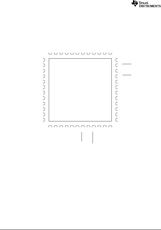
|||||||||||||||||||||||||||||||||||||||||||
|
|
|
|
|
|
|
|
|
|
|
|
|
|
|
|
|
|
|
|
|
|
|
|
|
|
|
|
|
|
|
|
|
|
|
|
RSL PACKAGE |
|
|
|
|
|
|
|
|
|
|
|
|
|
|
|
|
|
|
|
|
|
|
|
|
|
|||||||||||||||||||
|
|
|
|
|
|
|
|
|
|
|
|
|
|
|
|
|
|
|
|
|
|
|
|
|
|
|
|
|
|
|
|
|
|
|
|
|
|
|
|
48 PINS |
|
|
|
|
|
|
|
|
|
|
|
|
|
|
|
|
|
|
|
|
|
|
|
|
|
|
|
|
|
|||||||||||
|
|
|
|
|
|
|
|
|
|
|
|
|
|
|
|
|
|
|
|
|
|
|
|
|
|
|
|
|
|
|
|
|
|
|
|
|
(TOP VIEW) |
|
|
|
|
|
|
|
|
|
|
|
|
|
|
|
|
|
|
|
|
|
|
|
|
|
||||||||||||||||||
|
|
|
|
|
|
|
|
|
|
|
|
V5 |
|
|
|
CDH1 |
|
|
|
CBST1 |
|
|
|
CSW1 |
|
|
|
CDL1 |
|
|
|
|
|
V5DRV |
|
|
|
PGND |
|
CDL2 |
|
|
|
CSW2 |
|
|
|
CBST2 |
|
|
|
CDH2 |
|
VBAT |
|
|||||||||||||||||||||||||
|
|
|
|
|
|
|
|
|
|
|
|
|
|
|
|
|
|
|
|
|
|
|
|
|
|
|
|
|
|
|
|
|
|
|
|
|
|
|
|
|
|
|
|
|
|
|
|
|
|
|
|
|
|
|
|
|
|
|
|
|
|
|
|
|
|
|
|
|
|
|
|
|
|
|
|
|
|
|
|
|
|
|
|
|
CTHERM |
|
|
48 |
|
|
|
|
47 |
|
|
|
|
46 |
|
|
|
|
45 |
|
|
|
|
44 |
|
|
|
|
|
43 |
|
|
|
|
42 |
|
|
|
41 |
|
|
|
|
40 |
|
|
|
|
39 |
|
|
|
|
38 |
|
|
|
37 |
|
|
|
|
CPWM3 |
||||||||||||||
|
|
|
|
|
|
|
|
|
|
|
|
|
|
|
|
|
|
|
|
|
|
|
|
|
|
|
|
|
|
|
|
|
|
|
|
|
|
|
|
|||||||||||||||||||||||||||||||||||||||||
|
|
|
|
|
|
|
|
|
|
|
|
|
|
|
|
|
|
|
|
|
|
|
|
|
|
|
|
|
|
|
|
|
|
|
|
|
|
|
|
|
|
|
|
|
|
|
|
|
|
|
|
|
|
|
|
|
|
|
|
|
|
|
|
|
|
|
|
|
|
|
|
|
|
|
|
|
||||
|
|
|
|
|
|
1 |
|
|
|
|
|
|
|
|
|
|
|
|
|
|
|
|
|
|
|
|
|
|
|
|
|
|
|
|
|
|
|
|
|
|
|
|
|
|
|
|
|
|
|
|
|
|
|
|
|
|
|
|
|
|
|
|
|
|
|
|
|
|
|
36 |
|
|||||||||
|
|
|
|
|
COCP-I |
|
|
|
|
|
|
|
|
|
|
|
|
|
|
|
|
|
|
|
|
|
|
|
|
|
|
|
|
|
|
|
|
|
|
|
|
|
|
|
|
|
|
|
|
|
|
|
|
|
|
|
|
|
|
|
|
|
|
|
|
|
|
|
|
|
|
|
|
|
|
|
|
|
CSKIP |
|
|
|
|
|
|
|
2 |
|
|
|
|
|
|
|
|
|
|
|
|
|
|
|
|
|
|
|
|
|
|
|
|
|
|
|
|
|
|
|
|
|
|
|
|
|
|
|
|
|
|
|
|
|
|
|
|
|
|
|
|
|
|
|
|
|
|
|
|
|
|
|
35 |
|
|||||||||
|
|
|
|
|
CIMON |
|
|
|
|
|
|
|
|
|
|
|
|
|
|
|
|
|
|
|
|
|
|
|
|
|
|
|
|
|
|
|
|
|
|
|
|
|
|
|
|
|
|
|
|
|
|
|
|
|
|
|
|
|
|
|
|
|
|
|
|
|
|
|
|
|
|
|
|
|
|
|
|
|
GPWM |
|
|
|
|
|
|
|
3 |
|
|
|
|
|
|
|
|
|
|
|
|
|
|
|
|
|
|
|
|
|
|
|
|
|
|
|
|
|
|
|
|
|
|
|
|
|
|
|
|
|
|
|
|
|
|
|
|
|
|
|
|
|
|
|
|
|
|
|
|
|
|
|
34 |
|
|||||||||
|
|
|
|
|
CCSP1 |
|
|
|
|
|
|
|
|
|
|
|
|
|
|
|
|
|
|
|
|
|
|
|
|
|
|
|
|
|
|
|
|
|
|
|
|
|
|
|
|
|
|
|
|
|
|
|
|
|
|
|
|
|
|
|
|
|
|
|
|
|
|
|
|
|
|
|
|
|
|
|
|
|
GSKIP |
|
|
|
|
|
|
|
4 |
|
|
|
|
|
|
|
|
|
|
|
|
|
|
|
|
|
|
|
|
|
|
|
|
|
|
|
|
|
|
|
|
|
|
|
|
|
|
|
|
|
|
|
|
|
|
|
|
|
|
|
|
|
|
|
|
|
|
|
|
|
|
|
33 |
|
|||||||||
|
|
|
|
|
CCSN1 |
|
|
|
|
|
|
|
|
|
|
|
|
|
|
|
|
|
|
|
|
|
|
|
|
|
|
|
|
|
|
|
|
|
|
|
|
|
|
|
|
|
|
|
|
|
|
|
|
|
|
|
|
|
|
|
|
|
|
|
|
|
|
|
|
|
|
|
|
|
|
|
|
|
GTHERM |
|
|
|
|
|
|
5 |
|
|
|
|
|
|
|
|
|
|
|
|
|
|
|
|
|
|
|
|
|
|
|
|
|
|
|
|
|
|
|
|
|
|
|
|
|
|
|
|
|
|
|
|
|
|
|
|
|
|
|
|
|
|
|
|
|
|
|
|
|
|
|
32 |
|
||||||||||
|
|
|
|
|
CCSN2 |
|
|
|
|
|
|
|
|
|
|
|
|
|
|
|
|
|
|
|
|
|
|
|
|
|
|
|
|
|
TPS51640A |
|
|
|
|
|
|
|
|
|
|
|
|
|
|
|
|
|
|
|
|
|
|
|
|
GOCP-I |
||||||||||||||||||||
|
|
|
|
|
6 |
|
|
|
|
|
|
|
|
|
|
|
|
|
|
|
|
|
|
|
|
|
|
|
|
|
|
|
|
|
|
|
|
|
|
|
|
|
|
|
|
|
|
31 |
||||||||||||||||||||||||||||||||
|
|
|
|
|
|
|
|
|
|
|
|
|
|
|
|
|
|
|
|
|
|
|
|
|
|
|
|
|
|
|
|
TPS59640 |
|
|
|
|
|
|
|
|
|
|
|
|
|
|
|
|
|
|
|
|
|
|
||||||||||||||||||||||||||
|
|
|
|
|
CCSP2 |
|
|
|
|
|
|
|
|
|
|
|
|
|
|
|
|
|
|
|
|
|
|
|
|
|
|
|
|
|
|
|
|
|
|
|
|
|
|
|
|
|
|
|
|
|
|
|
|
|
|
|
|
|
|
|
|
|
|
|
GIMON |
|||||||||||||||
|
|
|
|
|
|
7 |
|
|
|
|
|
|
|
|
|
|
|
|
|
|
|
|
|
|
|
|
|
|
|
|
|
|
|
TPS59641 |
|
|
|
|
|
|
|
|
|
|
|
|
|
|
|
|
|
|
|
|
|
|
30 |
|
||||||||||||||||||||||
|
|
|
|
|
CCSP3 |
|
|
|
|
|
|
|
|
|
|
|
|
|
|
|
|
|
|
|
|
|
|
|
|
|
|
|
|
|
|
|
|
|
|
|
|
|
|
|
|
|
|
|
|
|
|
|
|
|
|
|
|
|
|
|
|
|
|
|
|
|
|
|
|
|
|
|
|
|
|
|
|
|
GCSP |
|
|
|
|
|
|
|
8 |
|
|
|
|
|
|
|
|
|
|
|
|
|
|
|
|
|
|
|
|
|
|
|
|
|
|
|
|
|
|
|
|
|
|
|
|
|
|
|
|
|
|
|
|
|
|
|
|
|
|
|
|
|
|
|
|
|
|
|
|
|
|
|
29 |
|
|||||||||
|
|
|
|
|
CCSN3 |
|
|
|
|
|
|
|
|
|
|
|
|
|
|
|
|
|
|
|
|
|
|
|
|
|
|
|
|
|
|
|
|
|
|
|
|
|
|
|
|
|
|
|
|
|
|
|
|
|
|
|
|
|
|
|
|
|
|
|
|
|
|
|
|
|
|
|
|
|
|
|
|
|
GCSN |
|
|
|
|
|
|
|
9 |
|
|
|
|
|
|
|
|
|
|
|
|
|
|
|
|
|
|
|
|
|
|
|
|
|
|
|
|
|
|
|
|
|
|
|
|
|
|
|
|
|
|
|
|
|
|
|
|
|
|
|
|
|
|
|
|
|
|
|
|
|
|
|
28 |
|
|||||||||
|
|
|
|
CCOMP |
|
|
|
|
|
|
|
|
|
|
|
|
|
|
|
|
|
|
|
|
|
|
|
|
|
|
|
|
|
|
|
|
|
|
|
|
|
|
|
|
|
|
|
|
|
|
|
|
|
|
|
|
|
|
|
|
|
|
|
|
|
|
|
|
|
|
|
|
|
|
|
|
|
GCOMP |
||
|
|
|
|
|
10 |
|
|
|
|
|
|
|
|
|
|
|
|
|
|
|
|
|
|
|
|
|
|
|
|
|
|
|
|
|
|
|
|
|
|
|
|
|
|
|
|
|
|
|
|
|
|
|
|
|
|
|
|
|
|
|
|
|
|
|
|
|
|
|
27 |
|
||||||||||
|
|
|
|
|
|
CVFB |
|
|
|
|
|
|
|
|
|
|
|
|
|
|
|
|
|
|
|
|
|
|
|
|
|
|
|
|
|
|
|
|
|
|
|
|
|
|
|
|
|
|
|
|
|
|
|
|
|
|
|
|
|
|
|
|
|
|
|
|
|
|
|
|
|
|
|
|
|
|
|
|
|
GVFB |
|
|
|
|
|
|
|
11 |
|
|
|
|
|
|
|
|
|
|
|
|
|
|
|
|
|
|
|
|
|
|
|
|
|
|
|
|
|
|
|
|
|
|
|
|
|
|
|
|
|
|
|
|
|
|
|
|
|
|
|
|
|
|
|
|
|
|
|
|
|
|
|
26 |
|
||||||||
|
|
|
|
|
CGFB |
|
|
|
|
|
|
|
|
|
|
|
|
|
|
|
|
|
|
|
|
|
|
|
|
|
|
|
|
|
|
|
|
|
|
|
|
|
|
|
|
|
|
|
|
|
|
|
|
|
|
|
|
|
|
|
|
|
|
|
|
|
|
|
|
|
|
|
|
|
|
|
|
|
GGFB |
|
|
|
|
|
|
|
12 |
|
|
|
|
|
|
|
|
|
|
|
|
|
|
|
|
|
|
|
|
|
|
|
|
|
|
|
|
|
|
|
|
|
|
|
|
|
|
|
|
|
|
|
|
|
|
|
|
|
|
|
|
|
|
|
|
|
|
|
|
|
|
|
25 |
|
|||||||||
|
|
|
|
|
|
|
|
|
13 |
|
|
|
|
14 |
|
|
|
|
15 |
|
|
|
|
16 |
|
|
|
|
17 |
|
|
|
|
18 |
|
|
|
|
19 |
|
|
|
|
20 |
|
|
|
|
21 |
|
|
|
|
22 |
|
|
|
|
23 |
|
|
|
24 |
|
|
|
|
|
||||||||||||
|
|
|
|
|
|
|
|
|
|
|
|
|
|
|
|
|
|
|
|
|
|
|
|
|
|
|
|
|
|
|
|
|
|
|
|
|
|
|
|
|
|
|
|
|
|
|||||||||||||||||||||||||||||||||||
|
|
|
|
|
|
|
|
|
|
|
|
|
|
|
|
|
|
|
|
|
|
|
|
|
|
|
|
|
|
|
|
|
|
|
|
|
|
|
|
|
|
|
|
|
|
|||||||||||||||||||||||||||||||||||
|
|
|
|
|
|
|
|
|
|
|
|
|
|
|
|
|
|
|
|
|
|
|
|
|
|
|
|
|
|
|
|
|
|
|
|
|
|
|
|
|
|
|
|
|
|
|
|
|
|
|
|
|
|
|
|
|
|
|
|
|
|
|
|
|
|
|
|
|
|
|
|
|
|
|
|
|
|
|
|
|
|
|
|
|
|
|
|
|
|
|
|
|
CF-IMAX |
|
|
|
VREF |
|
|
|
V3R3 |
|
|
|
VR_ON |
|
|
|
CPGOOD |
|
|
|
|
|
VCLK |
|
|
|
ALERT |
|
VDIO |
|
|
|
VR_HOT |
|
|
|
SLEWA |
|
|
|
GPGOOD |
|
GF-IMAX |
|
|||||||||||||||||||||||||
PIN FUNCTIONS |
|
|
|
|
|
|
|
|
|
|
|
|
|
|
|
|
|
|
|
|
|
|
|
|
|
|
|
|
|
|
|
|
|
|
|
|
|
|
|
|
|
|
|
|
|
|
|
|
|
|
|
|
|
|
|
|
|
|
|
|
|
|
|
|
|
|
|
|
|
|
|
|
|
|
|
|
||||
|
|
|
|
|
|
|
|
|
|
|
|
|
|
|
|
|
|
|
|
|
|
|
|
|
|
|
|
|
|
|
|
|
|
|
|
|
|
|
|
|
|
|
|
|
|
|
|
|
|
|
|
|
|
|
|
|
|
|
|
|
|
|
|
|
|
|
|
|
|
|
|
|
|
|
|
|
|
|
|
|
|
|
PIN |
|
I/O |
|
|
|
|
|
|
|
|
|
|
|
|
|
|
|
|
|
|
|
|
|
|
|
|
|
|
|
|
|
|
|
|
|
|
|
|
|
|
|
|
|
|
|
|
|
|
|
DESCRIPTION |
|
|
|
|
|
|
|
|||||||||||||||||||||
|
|
|
|
|
|
|
|
|
|
|
|
|
|
|
|
|
|
|
|
|
|
|
|
|
|
|
|
|
|
|
|
|
|
|
|
|
|
|
|
|
|
|
|
|
|
|
|
|
|
|
|
|
|
|
|
|
|
|||||||||||||||||||||||
|
NAME |
NO. |
|
|
|
|
|
|
|
|
|
|
|
|
|
|
|
|
|
|
|
|
|
|
|
|
|
|
|
|
|
|
|
|
|
|
|
|
|
|
|
|
|
|
|
|
|
|
|
|
|
|
|
|
|
|
||||||||||||||||||||||||
|
|
|
|
|
|
|
|
|
|
|
|
|
|
|
|
|
|
|
|
|
|
|
|
|
|
|
|
|
|
|
|
|
|
|
|
|
|
|
|
|
|
|
|
|
|
|
|
|
|
|
|
|
|
|
|
|
|
|
|
|
|
|
|
|
|
|
|
|
|
|
|
|
|
|
|
|
|
|||
|
|
|
|
|
|
|||||||||||||||||||||||||||||||||||||||||||||||||||||||||||||||||||||||||||
|
|
|
19 |
O |
SVID interrupt line, open drain. Route between VCLK and VDIO to prevent cross-talk. |
|||||||||||||||||||||||||||||||||||||||||||||||||||||||||||||||||||||||||||
|
ALERT |
|||||||||||||||||||||||||||||||||||||||||||||||||||||||||||||||||||||||||||||||
|
CBST1 |
46 |
I |
Top N-channel FET bootstrap voltage input for CPU phase 1. |
|
|
|
|
|
|
|
|
|
|
|
|
|
|||||||||||||||||||||||||||||||||||||||||||||||||||||||||||||||
|
|
|
|
|
|
|
|
|
|
|
|
|
|
|
|
|
|
|
|
|
|
|
|
|
||||||||||||||||||||||||||||||||||||||||||||||||||||||||
|
CBST2 |
39 |
I |
Top N-channel bootstrap voltage input for CPU phase 2. |
|
|
|
|
|
|
|
|
|
|
|
|
|
|
|
|
|
|
|
|||||||||||||||||||||||||||||||||||||||||||||||||||||||||
|
|
|
|
|
|
|
|
|
|
|
|
|
|
|
|
|
|
|
|
|
|
|
|
|
|
|
|
|
|
|
|
|
|
|
|
|
|
|
|
|
|
|
|
|
|
|
|
|
|
|
|
|
|
|
|
|
|
|
|
|
|
|
|
|
|
|
|
|
|
|
|
|
|
|
|
|
|
|
|
|
|
CCSN1 |
5 |
|
|
Negative current sense inputs for the CPU converter. Connect to the most negative node of current sense |
|||||||||||||||||||||||||||||||||||||||||||||||||||||||||||||||||||||||||||
|
|
|
|
|
|
|||||||||||||||||||||||||||||||||||||||||||||||||||||||||||||||||||||||||||
|
CCSN2 |
6 |
I |
|
||||||||||||||||||||||||||||||||||||||||||||||||||||||||||||||||||||||||||||
|
|
resistor or inductor DCR sense network. CCSN1 has a secondary OVP comparator. |
||||||||||||||||||||||||||||||||||||||||||||||||||||||||||||||||||||||||||||||
|
|
|
|
|
|
|||||||||||||||||||||||||||||||||||||||||||||||||||||||||||||||||||||||||||
|
CCSN3 |
9 |
|
|
||||||||||||||||||||||||||||||||||||||||||||||||||||||||||||||||||||||||||||
|
|
|
|
|
|
|
|
|
|
|
|
|
|
|
|
|
|
|
|
|
|
|
|
|
|
|
|
|
|
|
|
|
|
|
|
|
|
|
|
|
|
|
|
|
|
|
|
|
|
|
|
|
|
|
|
|
|
|
|
|
|
|
|
|
|
|
|
|
|
|
|
|
|
|
|
|
|
|||
|
|
|
|
|
|
|||||||||||||||||||||||||||||||||||||||||||||||||||||||||||||||||||||||||||
|
CCOMP |
10 |
O |
Output of GM error amplifier for the CPU converter. A resistor to VREF sets the droop gain. |
||||||||||||||||||||||||||||||||||||||||||||||||||||||||||||||||||||||||||||
|
|
|
|
|
|
|
|
|
|
|
|
|
|
|
|
|
|
|
|
|
|
|
|
|
|
|
|
|
|
|
|
|
|
|
|
|
|
|
|
|
|
|
|
|
|
|
|
|
|
|
|
|
|
|
|
|
|
|
|
|
|
|
|
|
|
|
|
|
|
|
|
|
|
|
|
|
|
|
|
|
|
CCSP1 |
4 |
|
|
Positive current sense inputs for the CPU converter. Connect to the most positive node of current sense resistor |
|||||||||||||||||||||||||||||||||||||||||||||||||||||||||||||||||||||||||||
|
|
|
|
|
|
|||||||||||||||||||||||||||||||||||||||||||||||||||||||||||||||||||||||||||
|
|
|
|
|
|
|||||||||||||||||||||||||||||||||||||||||||||||||||||||||||||||||||||||||||
|
CCSP2 |
7 |
I |
or inductor DCR sense network. Tie CCSP3, 2 or 1 (in that order) to V3R3 to disable the phase. Tie CCSP1 to |
||||||||||||||||||||||||||||||||||||||||||||||||||||||||||||||||||||||||||||
|
|
|
|
|
|
V3R3 to run the GPU converter only. |
|
|
|
|
|
|
|
|
|
|
|
|
|
|
|
|
|
|
|
|
|
|
|
|
|
|
|
|
|
|
|
|
|
|
|
|
||||||||||||||||||||||||||||||||||||||
|
CCSP3 |
8 |
|
|
|
|
|
|
|
|
|
|
|
|
|
|
|
|
|
|
|
|
|
|
|
|
|
|
|
|
|
|
|
|
|
|
|
|
|
|
||||||||||||||||||||||||||||||||||||||||
|
|
|
|
|
|
|
|
|
|
|
|
|
|
|
|
|
|
|
|
|
|
|
|
|
|
|
|
|
|
|
|
|
|
|
|
|
|
|
|
|
|
|
|
|
|
|
|
|
|
|
|
|
|
|
|
|
|
|
|
|
|
|
|
|
|
|
|
|
|
|
|
|
|
|
|
|
|
|||
|
|
|
|
|
|
|
|
|
|
|
|
|
|
|
|
|
|
|
|
|
|
|
|
|
||||||||||||||||||||||||||||||||||||||||||||||||||||||||
|
CDH1 |
47 |
O |
Top N-channel FET gate drive output for CPU phase 1. |
|
|
|
|
|
|
|
|
|
|
|
|
|
|
|
|
|
|
|
|||||||||||||||||||||||||||||||||||||||||||||||||||||||||
|
|
|
|
|
|
|
|
|
|
|
|
|
|
|
|
|
|
|
|
|
|
|
|
|
||||||||||||||||||||||||||||||||||||||||||||||||||||||||
|
CDH2 |
38 |
O |
Top N-channel FET gate drive output for CPU phase 2. |
|
|
|
|
|
|
|
|
|
|
|
|
|
|
|
|
|
|
|
|||||||||||||||||||||||||||||||||||||||||||||||||||||||||
|
|
|
|
|
|
|
|
|
|
|
|
|
||||||||||||||||||||||||||||||||||||||||||||||||||||||||||||||||||||
|
CDL1 |
44 |
O |
Synchronous N-channel FET gate drive output for CPU phase 1. |
|
|
|
|
|
|
|
|||||||||||||||||||||||||||||||||||||||||||||||||||||||||||||||||||||
|
|
|
|
|
|
|
|
|
|
|
|
|
||||||||||||||||||||||||||||||||||||||||||||||||||||||||||||||||||||
|
CDL2 |
41 |
O |
Synchronous N-channel FET gate drive output for CPU phase 2. |
|
|
|
|
|
|
|
|||||||||||||||||||||||||||||||||||||||||||||||||||||||||||||||||||||
|
|
|
|
|
|
|
|
|
|
|
|
|
|
|
|
|
|
|
|
|
|
|
|
|
|
|
|
|
|
|
|
|
|
|
|
|
|
|
|
|
|
|
|
|
|
|
|
|
|
|
|
|
|
|
|
|
|
|
|
|
|
|
|
|
|
|
|
|
|
|
|
|
|
|
|
|
|
|
|
|
10 |
Submit Documentation Feedback |
Copyright © 2012, Texas Instruments Incorporated |
|
|
|
|
|
|
|
|
|
TPS51640A, TPS59640, TPS59641 |
www.ti.com |
|
|
|
|
|
|
SLUSAQ2 –JANUARY 2012 |
||
|
|
|
|
|
|
|
|
|
|
|
|
PIN |
|
I/O |
|
|
DESCRIPTION |
||
|
|
|
|
|
|
||||
|
NAME |
NO. |
|
|
|||||
|
|
|
|
|
|
|
|||
|
|
|
|
|
|
||||
|
|
|
|
|
Voltage divider to VREF. A resistor to GND sets the operating frequency of the CPU converter. The voltage level |
||||
|
CF-IMAX |
13 |
I |
sets the maximum operating current of the CPU converter. The IMAX value is an 8-bit A/D where VIMAX = VREF × |
|||||
|
|
|
|
|
IMAX / 255. Both are latched at start-up. |
||||
|
CGFB |
12 |
I |
Voltage sense return tied for the CPU converter. Tie to GND with a 10-Ω resistor to close feedback when the |
|||||
|
microprocessor is not in the socket. |
||||||||
|
|
|
|
|
|||||
|
|
|
|
|
|
||||
|
CIMON |
3 |
O |
Analog current monitor output for the CPU converter. VCIMON = ΣVCS × ACS × (1 + RCIMON/RCOCP). Connect a |
|||||
|
220-nF capacitor to GND for stability. |
||||||||
|
|
|
|
|
|||||
|
COCP-I |
2 |
I |
Resistor to GND (RCOCP) selects 1 of 8 OCP levels (per phase, latched at start-up) of the CPU converter. Also, |
|||||
|
|
|
|
|
voltage divider to CIMON. Resistor ratio sets the IMON gain (see CIMON pin description). |
||||
|
CPGOOD |
17 |
O |
IMVP-7_PWRGD output for the CPU converter. Open-drain. |
|||||
|
|
|
|
|
|||||
|
CSW1 |
45 |
I/O |
Top N-channel FET gate drive return for CPU phase 1. |
|||||
|
|
|
|
|
|||||
|
CSW2 |
40 |
I/O |
Top N-channel FET gate drive return for CPU phase 2. |
|||||
|
|
|
|
|
|||||
|
CPWM3 |
36 |
O |
PWM control for the external driver, 5V logic level. |
|||||
|
|
|
|
|
|
||||
|
|
|
|
|
Skip mode control of the external driver for the CPU converter. A logic HI = FCCM, LO = SKIP. R to GND selects |
||||
|
CSKIP |
35 |
O |
||||||
|
|
|
|
|
|
||||
|
1 of 8 OSR/USR levels. 0.1 V < VCSKIP < 0.3 V at start-up turns OSR off. |
||||||||
|
|
|
|
|
|||||
|
CTHERM |
1 |
I/O |
Thermal sensor connection for the CPU converter. A resistor connected to VREF forms a divider with an NTC |
|||||
|
thermistor connected to GND. |
||||||||
|
|
|
|
|
|
|
|
||
|
CVFB |
11 |
I |
Voltage sense line tied directly to VCORE of the CPU converter. Tie to VCORE with a 10-Ω resistor to close |
|||||
|
feedback when µP is not in the socket. The soft-stop transistor is on this pin |
||||||||
|
|
|
|
|
|||||
|
|
|
|
|
Negative current sense input for the GPU converter. Connect to the most negative node of current sense resistor |
||||
|
GCSN |
28 |
I |
or inductor DCR sense network. GCSN has a secondary OVP comparator and includes the soft-stop pull-down |
|||||
|
|
|
|
|
transistor. |
||||
|
|
|
|
|
|
|
|
||
|
GCSP |
29 |
I |
Positive current sense input for the GPU converter. Connect to the most positive node of current sense resistor |
|||||
|
or inductor DCR sense network. Tie to V3R3 to disable the GPU converter. |
||||||||
|
|
|
|
|
|||||
|
|
|
|
|
|
|
|
||
|
GCOMP |
27 |
O |
Output of gM error amplifier for the GPU converter. A resistor to VREF sets the droop gain. |
|||||
|
GGFB |
25 |
I |
Voltage sense return tied for the GPU converter. Tie to GND with a 10-Ω resistor to close feedback when the |
|||||
|
microprocessor is not in the socket. |
||||||||
|
|
|
|
|
|||||
|
|
|
|
|
|
|
|
||
|
|
|
24 |
I |
Voltage divider to VREF. R to GND sets the operating frequency of the GPU converter. The voltage level sets |
||||
|
GF-IMAX |
|
|
the maximum operating current of the GPU converter. The IMAX value is an 8-bit A/D where VIMAX = VREF × |
|||||
|
|
|
|
|
IMAX / 255. Both are latched at start-up. |
||||
|
GIMON |
30 |
O |
Analog current monitor output for the GPU converter. VGIMON = VISENSE × (1 + RGIMON/RGOCP). Connect a |
|||||
|
|
|
220-nF capacitor to GND for stability. |
||||||
|
|
|
|
|
|||||
|
GOCP-I |
31 |
I |
Voltage divider to GIMON. Resistor ratio sets the IMON gain (see GIMON pin). Resistor to GND (RGOCP) selects |
|||||
|
|
|
|
|
1 of 8 OCP levels (per phase, latched at start-up) of the GPU converter. |
||||
|
GPGOOD |
23 |
O |
IMVP-7_PWRGD output for the GPU converter. Open-drain. |
|||||
|
|
|
|
|
|
|
|
||
|
GPWM |
34 |
O |
PWM control for the external driver, 5-V logic level. |
|||||
|
|
|
|
|
|
|
|
||
|
|
|
33 |
O |
Skip mode control of the external driver for the GPU converter, 5-V logic level. Logic HI = FCCM, LO = SKIP. R |
||||
|
GSKIP |
||||||||
|
|
|
to GND selects 1 of 8 OSR/USR levels. 0.1 V < V |
|
< 0.3 V at start-up turns OSR off. |
||||
|
|
|
|
|
GSKIP |
||||
|
GTHERM |
32 |
I/O |
Thermal sensor input for the GPU converter. A resistor connected to VREF forms a divider with an NTC |
|||||
|
|
|
thermistor connected to GND. |
||||||
|
|
|
|
|
|||||
|
|
|
|
|
|
|
|
|
|
|
GVFB |
26 |
I |
Voltage sense line tied directly to VGFX of the GPU converter. Tie to VGFX with a 10-Ω resistor to close feedback |
|||||
|
|
|
when the microprocessor is not in the socket. The soft-stop transistor is on this pin |
||||||
|
|
|
|
|
|||||
|
PGND |
42 |
– |
Synchronous N-channel FET gate drive return. |
|||||
|
SLEWA |
22 |
I |
The voltage at start-up sets 1 of 7 slew rates for both converters. The SLOW rate is SLEWRATE/4. Soft-start |
|||||
|
|
|
and soft-stop rates are SLEWRATE/8. This value is latched at start-up. Tie to GND to disable SCLK timer. |
||||||
|
|
|
|
|
|||||
|
|
|
|
|
|
|
|
|
|
|
V5 |
48 |
I |
5-V power input for analog circuits; connect through resistor to 5-V plane and bypass to GND with ≥1 µF ceramic |
|||||
|
|
|
capacitor |
||||||
|
|
|
|
|
|||||
|
V5DRV |
43 |
I |
Power input for the gate drivers; connected with an external resistor to V5F; decouple with a ≥2.2 µF ceramic |
|||||
|
|
|
capacitor. |
||||||
|
|
|
|
|
|||||
|
V3R3 |
15 |
I |
3.3-V power input; bypass to GND with ≥1 µF ceramic cap. |
|||||
|
VBAT |
37 |
I |
Provides VBAT information to the on-time circuits for both converters. A 10-kΩ series resistor protects the |
|||||
|
|
|
adjacent pins from inadvertent shorts due to solder bridges or mis-probing during test. |
||||||
|
|
|
|
|
|||||
|
VCLK |
18 |
I |
SVID clock. 1-V logic level. |
|||||
|
|
|
|
|
|
|
|
|
|
|
VDIO |
20 |
I/O |
SVID digital I/O line. 1-V logic level. |
|||||
|
|
|
|
|
|
|
|
|
|
|
VREF |
14 |
O |
1.7-V, 500-µA reference. Bypass to GND with a 0.22-µF ceramic capacitor. |
|||||
|
|
|
|
|
|
|
|
|
|
Copyright © 2012, Texas Instruments Incorporated |
Submit Documentation Feedback |
11 |

TPS51640A, TPS59640, TPS59641
SLUSAQ2 –JANUARY 2012 |
www.ti.com |
||||
|
|
|
|
|
|
|
PIN |
|
I/O |
DESCRIPTION |
|
|
|
|
|
||
|
NAME |
NO. |
|||
|
|
|
|||
|
|
|
|
|
|
|
VR_ON |
16 |
I |
IMVP-7 VR enable; 1V I/O level; 100-ns de-bounce. Regulator enters controlled soft-stop when brought low. |
|
|
|
|
|
|
|
|
|
|
21 |
O |
IMVP-7 thermal flag open drain output – active low. Typically pulled up to 1-V logic level through 56 Ω. Fall time |
|
VR_HOT |
||||
|
|
|
< 100 ns. 1-ms de-glitch using consecutive 1-ms samples. |
||
|
|
|
|
|
|
|
PAD |
GND |
– |
Thermal pad and analog circuit reference; tie to a quiet area in the system ground plane with multiple vias. |
|
12 |
Submit Documentation Feedback |
Copyright © 2012, Texas Instruments Incorporated |
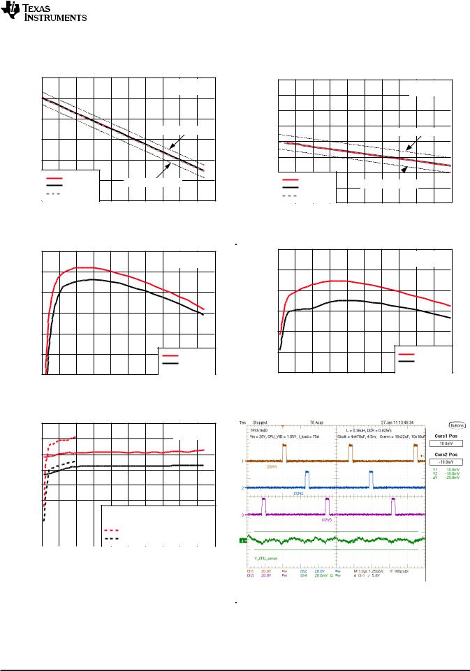
TPS51640A, TPS59640, TPS59641
www.ti.com |
SLUSAQ2 –JANUARY 2012 |
TYPICAL CHARACTERISTICS
3-Phase Configuration, 94-A CPU
|
|
|
|
|
|
|
|
|
VVID = 1.05 V |
||
|
1.05 |
|
|
|
|
|
|
|
|
|
|
(V) |
1.00 |
|
|
|
|
|
|
|
|
|
|
Voltage |
|
|
|
|
|
|
|
Specified Maximum |
|||
0.95 |
|
|
|
|
|
|
|
|
|
|
|
|
|
|
|
|
|
|
|
|
|
|
|
Output |
0.90 |
|
|
|
|
|
|
|
|
|
|
|
|
|
|
|
|
|
|
|
|
|
|
|
0.85 |
|
VIN = 9 V |
|
Specified Minimum |
|
|
||||
|
|
|
VIN = 20 V |
|
|
|
|
|
|
|
|
|
|
|
Nominal |
|
|
|
|
|
|
|
|
|
0.80 |
|
|
|
|
|
|
|
|
|
|
|
0 |
10 |
20 |
30 |
40 |
50 |
60 |
70 |
80 |
90 |
100 |
|
|
|
|
|
Output Current (A) |
|
|
|
|||
|
0.700 |
|
|
|
|
|
|
|
|
|
|
|
0.675 |
|
|
|
|
|
|
|
VVID = 0.6 V |
|
|
|
|
|
|
|
|
|
|
|
|
|
|
(V) |
0.650 |
|
|
|
|
|
|
|
|
|
|
0.625 |
|
|
|
|
|
|
|
|
|
|
|
Voltage |
|
|
|
|
|
|
|
|
|
|
|
|
|
|
|
|
|
|
Specified Maximum |
||||
0.600 |
|
|
|
|
|
|
|
|
|
|
|
|
|
|
|
|
|
|
|
|
|
|
|
Output |
0.575 |
|
|
|
|
|
|
|
|
|
|
|
|
|
|
|
|
|
|
|
|
|
|
|
0.550 |
|
|
|
|
|
|
|
|
|
|
|
0.525 |
|
VIN = 9 V |
|
Specified Minimum |
|
|
||||
|
|
VIN |
= 20 V |
|
|
|
|
|
|
|
|
|
|
|
|
|
|
|
|
|
|
||
|
|
|
Nominal |
|
|
|
|
|
|
|
|
|
0.500 |
|
|
|
|
|
|
|
|
|
|
|
0 |
2 |
4 |
6 |
8 |
10 |
12 |
14 |
16 |
18 |
20 |
|
|
|
|
|
Output Current (A) |
|
|
|
|||
Figure 1. Output Voltage vs. Load Current in PS0
|
95 |
|
|
|
|
|
|
|
|
|
|
|
|
|
|
|
|
|
|
|
VVID = 1.05 V |
||
|
90 |
|
|
|
|
|
|
|
|
|
|
(%) |
85 |
|
|
|
|
|
|
|
|
|
|
|
|
|
|
|
|
|
|
|
|
|
|
Efficiency |
80 |
|
|
|
|
|
|
|
|
|
|
75 |
|
|
|
|
|
|
|
|
|
|
|
|
|
|
|
|
|
|
|
|
|
|
|
|
70 |
|
|
|
|
|
|
|
VIN |
= 9 V |
|
|
|
|
|
|
|
|
|
|
|
||
|
|
|
|
|
|
|
|
|
VIN = 20 V |
||
|
65 |
|
|
|
|
|
|
|
|
|
|
|
0 |
10 |
20 |
30 |
40 |
50 |
60 |
70 |
80 |
90 |
100 |
Output Current (A)
Figure 3. Efficiency vs. Load Current in PS0
Figure 2. Output Voltage vs. Load Current in PS1
|
|
|
|
|
|
|
|
|
VVID = 0.6 V |
|
|
|
90 |
|
|
|
|
|
|
|
|
|
|
(%) |
85 |
|
|
|
|
|
|
|
|
|
|
|
|
|
|
|
|
|
|
|
|
|
|
Efficiency |
80 |
|
|
|
|
|
|
|
|
|
|
75 |
|
|
|
|
|
|
|
|
|
|
|
|
|
|
|
|
|
|
|
|
|
|
|
|
70 |
|
|
|
|
|
|
|
VIN |
= 9 V |
|
|
|
|
|
|
|
|
|
|
|
||
|
|
|
|
|
|
|
|
|
VIN = 20 V |
||
|
65 |
|
|
|
|
|
|
|
|
|
|
|
0 |
2 |
4 |
6 |
8 |
10 |
12 |
14 |
16 |
18 |
20 |
Output Current (A)
Figure 4. Efficiency vs. Load Current in PS1
|
400 |
|
RCF = 24 kW |
|
350 |
|
300 |
(Hz) |
250 |
|
|
Frequency |
200 |
150 |
|
|
100 |
|
|
|
|
|
|
PS0, VVID = 1.05 V, VIN |
= 20 V |
|||||
|
|
|
|
|
|
||||||||
|
|
|
|
|
|
||||||||
50 |
|
|
|
|
|
|
PS0, VVID = 1.05 V, VIN |
= 9 |
V |
||||
|
|
|
|
|
|
||||||||
|
|
|
|
|
|
PS1, VVID = 1.05 |
V, VIN |
= 20 V |
|||||
|
|
|
|
|
|
||||||||
0 |
|
|
|
|
|
|
PS1, VVID = 1.05 |
V, VIN = 9 |
V |
||||
|
|
|
|
|
|
|
|
|
|
|
|
|
|
0 |
10 |
20 |
30 |
40 |
50 |
60 |
70 |
80 |
90 |
100 |
|||
|
|
|
|
|
|
Output Current (A) |
|
|
|
|
|
||
Figure 5. Frequency vs Load-Current (PS0 and PS1) Figure 6. Switching Ripple in PS0, VIN = 20 V
Copyright © 2012, Texas Instruments Incorporated |
Submit Documentation Feedback |
13 |
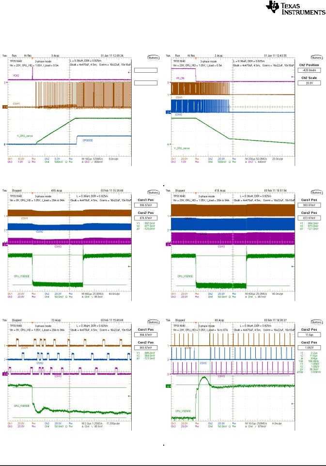
TPS51640A, TPS59640, TPS59641
SLUSAQ2 –JANUARY 2012 |
www.ti.com |
TYPICAL CHARACTERISTICS
3-Phase Configuration, 94-A CPU (continued)
Figure 7. Start-Up and PGOOD |
Figure 8. Soft-Stop |
(TPS51640A and TPS59640 Only) |
|
Figure 9. Load Transient, VIN = 9 V, Load step = 66 A |
Figure 10. Load Transient, VIN = 20 V, Load step = 66 A |
Figure 11. Load Insertion, VIN = 9 V, Load step = 66 A |
Figure 12. Load Release, VIN = 20 V, Load step = 66 A |
14 |
Submit Documentation Feedback |
Copyright © 2012, Texas Instruments Incorporated |
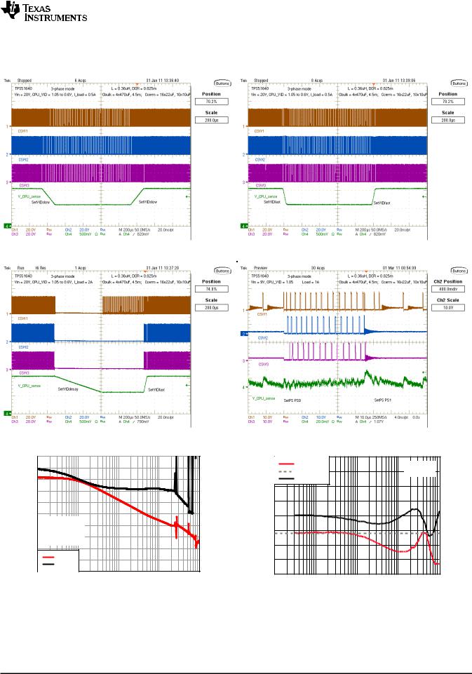
TPS51640A, TPS59640, TPS59641
www.ti.com |
SLUSAQ2 –JANUARY 2012 |
TYPICAL CHARACTERISTICS
3-Phase Configuration, 94-A CPU (continued)
Figure 13. Dynamic VID: SetVID-Slow/SetVID-Slow |
Figure 14. Dynamic VID: SetVID-Fast/SetVID-Fast |
|
|
Figure 15. SetVID-Decay/SetVID-Fast |
|
|||
|
50 |
|
|
|
225 |
|
|
40 |
|
|
|
180 |
|
|
30 |
|
|
|
135 |
|
Magnitude (dB) |
20 |
|
|
|
90 |
|
10 |
|
|
|
45 |
Phase (°) |
|
0 |
|
|
|
0 |
||
−10 |
3−Phase CPU |
|
|
−45 |
||
VOUT = 1.05 V |
|
|
||||
−20 |
|
|
−90 |
|||
|
IOUT ~ 20 A |
|
|
|
||
|
−30 |
|
|
|
−135 |
|
|
−40 |
Gain |
|
|
−180 |
|
|
Phase |
|
|
|
||
|
|
|
|
|
|
|
|
−50 |
1000 |
10000 |
100000 |
−225 |
|
|
100 |
1000000 |
|
|||
Frequency (Hz)
Figure 17. CPU Bode Plot
Figure 16. PS Change PS0 to PS1 Toggle
|
0.0045 |
|
|
|
80 |
|
|
|
Magnitude |
|
CPU |
|
|
|
0.004 |
Target |
|
3-Phase |
60 |
|
|
|
Phase |
|
|
|
|
(W) |
0.0035 |
|
|
|
40 |
|
0.003 |
|
|
|
20 |
(°) |
|
Magnitude |
0.0025 |
|
|
|
0 |
Phase |
|
|
|
|
|
||
0.002 |
|
|
|
-20 |
OUT |
|
OUT |
|
|
|
Z |
||
|
|
|
|
|
||
Z |
0.0015 |
|
|
|
-40 |
|
|
|
|
|
|
||
|
0.001 |
|
|
|
-60 |
|
|
0.0005 |
|
|
|
-80 |
|
|
100 |
1 k |
10 k |
100 k |
1 M |
|
Frequency (Hz)
Figure 18. Output Impedance
Copyright © 2012, Texas Instruments Incorporated |
Submit Documentation Feedback |
15 |
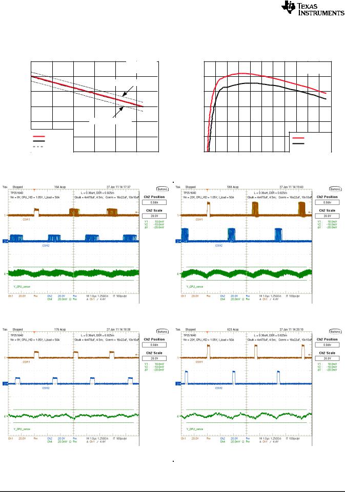
TPS51640A, TPS59640, TPS59641
SLUSAQ2 –JANUARY 2012 |
www.ti.com |
TYPICAL CHARACTERISTICS
2-Phase Configuration, 53-A CPU
|
1.10 |
|
|
|
|
|
|
|
|
|
|
|
|
VVID = 1.05 V |
|
|
1.05 |
|
|
|
|
|
|
|
|
|
|
|
Specified Maximum |
|
|
(V) |
1.00 |
|
|
|
|
|
|
Voltage |
0.95 |
|
|
|
|
|
|
|
|
|
|
|
|
|
|
Output |
0.90 |
|
|
Specified Minimum |
|
||
|
|
|
|
|
|
|
|
|
0.85 |
VIN |
= 9 V |
|
|
|
|
|
|
|
|
|
|
||
|
|
VIN |
= 20 V |
|
|
|
|
|
0.80 |
Nominal |
|
|
|
|
|
|
|
|
|
|
|
|
|
|
0 |
10 |
20 |
30 |
40 |
50 |
60 |
|
|
|
Output Current (A) |
|
|
||
Figure 19. Output Voltage Vs. Load Current in PS0
|
95 |
|
|
|
|
|
|
|
|
|
|
|
|
|
|
|
|
|
|
|
|
VVID = 1.05 V |
|
||
|
90 |
|
|
|
|
|
|
|
|
|
|
|
(%) |
85 |
|
|
|
|
|
|
|
|
|
|
|
|
|
|
|
|
|
|
|
|
|
|
|
|
Efficiency |
80 |
|
|
|
|
|
|
|
|
|
|
|
75 |
|
|
|
|
|
|
|
|
|
|
|
|
|
70 |
|
|
|
|
|
|
|
|
VIN = 9 V |
|
|
|
|
|
|
|
|
|
|
|
|
|
||
|
65 |
|
|
|
|
|
|
|
|
VIN = 20 V |
||
|
|
|
|
|
|
|
|
|
|
|
|
|
|
0 |
5 |
10 |
15 |
20 |
25 |
30 |
35 |
40 |
45 |
50 |
55 |
Output Current (A)
Figure 20. Efficiency Vs. Load Current in PS0
Figure 21. Switching Ripple in PS0 (Persistence), |
Figure 22. Switching Ripple in PS0 (Persistence), |
VIN = 9 V |
VIN = 20 V |
Figure 23. Switching Ripple in PS0, VIN = 9 V |
Figure 24. Switching Ripple in PS0, VIN = 20 V |
16 |
Submit Documentation Feedback |
Copyright © 2012, Texas Instruments Incorporated |

TPS51640A, TPS59640, TPS59641
www.ti.com |
SLUSAQ2 –JANUARY 2012 |
TYPICAL CHARACTERISTICS
2-Phase Configuration, 53-A CPU (continued)
Figure 25. Load Transient, VIN = 9 V, Load Step = 43 A |
Figure 26. Load Transient, VIN = 20 V, Load Step = 43 A |
Figure 27. Load Insertion, VIN = 9 V, Load Step = 43 A, |
Figure 28. Load Release, VIN = 20 V, Load Step = 43 A, |
OSR/USR Setting 150 kΩ) |
OSR/USR Setting 150 kΩ) |
Figure 29. Load Insertion, VIN = 9 V, Load Step = 43 A, |
Figure 30. Load Release,VIN = 20 V, Load Step = 43 A, |
OSR/USR Setting 39 kΩ (Reduced Output Capacitance) |
OSR/USR Setting 39 kΩ (Reduced Output Capacitance) |
Copyright © 2012, Texas Instruments Incorporated |
Submit Documentation Feedback |
17 |
Loading...