


 Loading...
Texas Instruments TPS2231MRGPR, TPS2231MRGPR-2, TPS2231MRGPR-3, TPS2231PW, TPS2231PWP Schematic [ru]
...RGP |
PW |
PWP |
DAP |
TPS2231
TPS2236
www.ti.com |
SLVS536J –JULY 2004 –REVISED SEPTEMBER 2009 |
ExpressCard™ POWER INTERFACE SWITCH
Check for Samples: TPS2231 TPS2236
FEATURES
•Meets the ExpressCard™ Standard (ExpressCard|34 or ExpressCard|54)
•Compliant with the ExpressCard™ Compliance Checklists
•Fully Satisfies the ExpressCard™ Implementation Guidelines
•Supports Systems with WAKE Function
•TTL-Logic Compatible Inputs
•Short Circuit and Thermal Protection
•–40°C to 85°C Ambient Operating Temperature Range
•Available in a 20-pin TSSOP, a 20-pin QFN, or
24-pin PowerPAD™ HTSSOP (Single)
•Available in a 32-pin PowerPAD™ HTSSOP (Dual)
APPLICATIONS
•Notebook Computers
•Desktop Computers
•Personal Digital Assistants (PDAs)
•Digital Cameras
•TV and Set Top Boxes
DESCRIPTION
The TPS2231 and TPS2236 ExpressCard power interface switches provide the total power management solution required by the ExpressCard specification. The TPS2231 and TPS2236 ExpressCard power interface switches distribute 3.3 V, AUX, and 1.5 V to the ExpressCard socket. Each voltage rail is protected with integrated current-limiting circuitry.
The TPS2231 supports systems with single-slot ExpressCard|34 or ExpressCard|54 sockets. The TPS2236 supports systems with dual-slot ExpressCard sockets.
End equipment for the TPS2231 and TPS2236 include notebook computers, desktop computers, personal digital assistants (PDAs), and digital cameras.
|
AUXIN |
AUXOUT |
|
|
Host |
3.3VIN |
3.3VOUT |
|
|
Power |
|
|
||
Source |
|
|
ConnectorHost |
ConnectorExpressCard |
|
SYSRST |
CPUSB |
||
|
1.5VIN |
1.5VOUT |
|
|
|
TPS2231 |
|
|
|
|
SHDN |
PERST |
|
Express Card |
|
|
|
||
|
|
|
|
|
|
STBY |
CPPE |
|
|
|
|
|
|
|
Host |
OC |
|
|
|
Chip |
|
|
|
|
Set/Lock |
GND |
RCLKEN |
|
|
Circuits |
|
|
REFCLK+ |
|
|
|
|
|
|
|
|
|
REFCLK− |
|
Please be aware that an important notice concerning availability, standard warranty, and use in critical applications of Texas Instruments semiconductor products and disclaimers thereto appears at the end of this data sheet.
PowerPAD is a trademark of Texas Instruments.
ExpressCard is a trademark of Personal Computer Memory Card International Association.
PRODUCTION DATA information is current as of publication date. |
Copyright © 2004–2009, Texas Instruments Incorporated |
Products conform to specifications per the terms of the Texas |
|
Instruments standard warranty. Production processing does not |
|
necessarily include testing of all parameters. |
|

TPS2231
TPS2236
SLVS536J –JULY 2004 –REVISED SEPTEMBER 2009 |
www.ti.com |
This integrated circuit can be damaged by ESD. Texas Instruments recommends that all integrated circuits be handled with appropriate precautions. Failure to observe proper handling and installation procedures can cause damage.
ESD damage can range from subtle performance degradation to complete device failure. Precision integrated circuits may be more susceptible to damage because very small parametric changes could cause the device not to meet its published specifications.
AVAILABLE OPTIONS
TA |
NUMBER OF CHANNELS |
|
PACKAGED DEVICES (1) |
(2) |
|
TSSOP |
PowerPAD HTSSOP |
|
QFN |
||
|
|
|
|||
|
|
|
|
|
|
|
|
|
|
|
TPS2231RGP |
|
|
|
|
|
|
|
|
|
|
|
TPS2231MRGP(3) |
–40°C to 85°C |
Single |
TPS2231PW |
TPS2231PWP |
|
TPS2231MRGP-1(4) |
|
|
|
|
|
TPS2231MRGP-2(5) |
|
|
|
|
|
TPS2231MRGP-3(6) |
|
Dual |
|
TPS2236DAP |
|
|
|
|
|
|
|
|
(1)The package is available taped and reeled. Add an R suffix to device types (e.g., TPS2231PWPR).
(2)For the most current package and ordering information, see the Package Option Addendum at the end of this document, or see the TI website at www.ti.com.
(3)The TPS2231MRGP is identical to the TPS2231 with the exception of the PowerPAD dimensions. See the Thermal Pad Mechanical data portion of this data sheet for specific information. The thermal pad for the TPS2231MRGP and TPS2231MRGP-1 is 2,2 mm × 2,2 mm; the thermal pad for the TPS2231RGP is 2,7 mm × 2,7 mm.
(4)The TPS2231MRGP-1 is identical to the TPS2231MGRP with the exception that the orientation of the part in the reel is rotated 180°. See the Package Materials Information portion of this data sheet for specific information.
(5)The TPS2231MRGP-2 is identical to the TPS2231MRGP with the exception that the orientation of the part in the reel is rotated 90° and does not have an internal pull-up resistor between AUX IN and SYSRST. See the Package Materials Information portion of this data sheet for specific information.
(6)The TPS2231MRGP-3 is identical to the TPS2231MRGP with the exception that the 1.5VIN and 3.3VIN UVLO circuits are independent.
ABSOLUTE MAXIMUM RATINGS
over operating free-air temperature range (unless otherwise noted)(1)
|
|
|
|
|
|
|
|
|
|
|
TPS223x |
UNIT |
|
|
|
|
|
|
|
|
|
|
|
|
|
|
|
Input voltage range for card |
VI(3.3VIN) |
|
|
|
|
|
–0.3 to 6 |
V |
||
VI |
|
VI(1.5VIN) |
|
|
|
|
|
–0.3 to 6 |
V |
|||
|
power |
|
|
|
|
|
||||||
|
|
VI(AUXIN) |
|
|
|
|
|
–0.3 to 6 |
V |
|||
|
|
|
|
|
|
|
|
|
|
|||
|
|
Logic input/output voltage |
|
|
|
|
|
|
–0.3 to 6 |
V |
||
|
|
|
|
|
|
|
|
|
|
|
|
|
|
|
|
|
|
VO(3.3VOUT) |
|
|
|
|
|
–0.3 to 6 |
V |
VO |
|
Output voltage range |
VO(1.5VOUT) |
|
|
|
|
|
–0.3 to 6 |
V |
||
|
|
|
|
|
VO(AUXOUT) |
|
|
|
|
|
–0.3 to 6 |
V |
|
|
Continuous total power dissipation |
|
|
|
|
|
See Dissipation Rating Table |
||||
|
|
|
|
|
|
|
|
|
|
|
|
|
|
|
|
|
|
IO(3.3VOUT) |
|
|
|
|
|
Internally limited |
|
IO |
|
Output current |
IO(AUXOUT) |
|
|
|
|
|
Internally limited |
|
||
|
|
|
|
|
IO(1.5VOUT) |
|
|
|
|
|
Internally limited |
|
|
|
OC |
sink current |
|
|
|
|
|
|
10 |
mA |
|
|
|
|
|
|
|
|
|
|
|
|
|
|
|
|
|
|
sink/source current |
|
|
|
|
|
|
10 |
mA |
|
|
PERST |
|
|
|
|
|
|
||||
TJ |
|
Operating virtual junction temperature range |
|
|
|
|
|
–40 to 120 |
°C |
|||
Tstg |
|
Storage temperature range |
|
|
|
|
|
|
–55 to 150 |
°C |
||
|
|
Lead temperature 1,6 mm (1/16 inch) from case for 10 seconds |
260 |
°C |
||||||||
|
|
|
|
|
|
|
|
|
|
|
|
|
|
|
|
|
|
|
TPS2231 |
|
|
||||
|
|
|
|
|
|
|
2 |
kV |
||||
|
|
Electrostatic discharge |
Human body model |
TPS2236, all pins except |
||||||||
ESD |
|
(HBM) MIL-STD-883C |
PERSTx and OCx |
|
|
|||||||
|
protection |
|
|
|||||||||
|
|
|
|
|
|
|
|
|
|
|||
|
|
TPS2236, PERSTx and OCx |
1.5 |
kV |
||||||||
|
|
|
|
|
|
|||||||
|
|
|
|
|
|
|
|
|
|
|
|
|
|
|
|
|
|
Charge device model (CDM) |
500 |
V |
|||||
|
|
|
|
|
|
|
|
|
|
|
|
|
(1)Stresses beyond those listed under absolute maximum ratings may cause permanent damage to the device. These are stress ratings only, and functional operation of the device at these or any other conditions beyond those indicated under recommended operating conditions is not implied. Exposure to absolute-maximum-rated conditions for extended periods may affect device reliability.
2 |
Submit Documentation Feedback |
Copyright © 2004–2009, Texas Instruments Incorporated |
Product Folder Link(s): TPS2231 TPS2236

|
TPS2231 |
|
TPS2236 |
www.ti.com |
SLVS536J –JULY 2004 –REVISED SEPTEMBER 2009 |
DISSIPATION RATINGS (Thermal Resistance = °C/W)
PACKAGE |
TA ≤ 25°C |
DERATING FACTOR |
TA = 70°C |
TA = 85°C |
|
POWER RATING |
ABOVE TA = 25°C |
POWER RATING |
POWER RATING |
||
|
|||||
PW (20)(1) |
704.2 mW |
7.41 mW/°C |
370.6 mW |
259.5 mW |
|
PWP (24)(1) |
3153 mW |
33.19 mW/°C |
1659.5 mW |
1161.6 mW |
|
RGP (20) (2) |
3277.5 mW |
34.5 mW/°C |
1725 mW |
1207.3 mW |
|
DAP (32) (1) |
993.4 mW |
10.46 mW/°C |
522.8 mW |
366 mW |
|
PowerPAD not soldered down |
|||||
|
|
|
|
||
|
|
|
|
|
|
DAP (32)(1) |
4040.8 mW |
42.55 mW/°C |
2126.8 mW |
1488.7 mW |
(1)These devices are mounted on an JEDEC low-k board (2-oz. traces on surface), (The table is assuming that the maximum junction temperature is 120°C). The power pad on the device must be soldered down to the power pad on the board if best thermal performance is needed.
(2)This device is mounted on a JEDEC JESO51.5 high-k board (2 signal, 2 plane). The values assume a maximum junction temperature of 120°C.
RECOMMENDED OPERATING CONDITIONS
|
|
|
MIN |
MAX |
UNIT |
|
|
|
|
|
|
VI(3.3VIN) |
|
3.3VIN is only required for its respective functions |
3 |
3.6 |
|
VI(1.5VIN) |
Input voltage |
1.5VIN is only required for its respective functions |
1.35 |
1.65 |
V |
VI(AUXIN) |
|
AUXIN is required for all circuit operations |
3 |
3.6 |
|
IO(3.3VOUT) |
|
|
0 |
1.3 |
A |
IO(1.5VOUT) |
Continuous output current |
TJ = 120°C |
0 |
650 |
mA |
IO(AUXOUT) |
|
|
0 |
275 |
mA |
TJ |
Operating virtual junction temperature |
–40 |
120 |
°C |
|
ELECTRICAL CHARACTERISTICS
TJ = 25°C, VI(3.3VIN) = VI(AUXIN) = 3.3 V, VI(1.5VIN) = 1.5 V, VI(/SHDNx), VI(/STBYx) = 3.3 V, VI(/CPPEx) = VI(/CPUSBx) = 0 V,
VI(/SYSRST) = 3.3 V, OCx and RCLKENx and PERSTx are open, all voltage outputs unloaded (unless otherwise noted)
|
|
PARAMETER |
TEST CONDITIONS |
MIN |
TYP |
MAX |
UNIT |
|
|
|
|
|
|
|
|
|
|
POWER SWITCH |
|
|
|
|
|
|
|
|
|
|
|
|
|
|
|
|
|
|
|
|
3.3VIN to 3.3VOUT with two switches |
TJ = 25°C, I = 1300 mA each |
|
45 |
|
mΩ |
|
|
|
on for dual |
TJ = 100°C, I = 1300 mA each |
|
|
68 |
|
|
|
|
|
|
|
|||
|
|
|
|
|
|
|
||
|
Power switch |
|
1.5VIN to 1.5VOUT With two switches |
TJ = 25°C, I = 650 mA each |
|
46 |
|
mΩ |
|
resistance |
|
on for dual |
TJ = 100°C, I = 650 mA each |
|
|
70 |
|
|
|
|
|
|
||||
|
|
|
|
|
|
|
||
|
|
|
AUXIN to AUXOUT with two switches |
TJ = 25°C, I = 275 mA each |
|
120 |
|
mΩ |
|
|
|
on for dual |
TJ = 100°C, I = 275 mA each |
|
|
200 |
|
|
|
|
|
|
|
|||
|
|
|
|
|
|
|
||
R(DIS_FET) |
Discharge resistance on 3.3V/1.5V/AUX outputs |
VI(/SHDNx) = 0 V, I(discharge) = 1 mA |
100 |
|
500 |
Ω |
||
|
Short-circuit |
|
IOS(3.3VOUT) (steady-state value) |
|
1.35 |
2 |
2.5 |
A |
IOS |
|
IOS(1.5VOUT) (steady-state value) |
TJ (–40, 120°C]. Output powered into a short |
0.67 |
1 |
1.3 |
A |
|
output current(1) |
|
|||||||
|
|
IOS(AUXOUT)(steady-state value) |
|
275 |
450 |
600 |
mA |
|
|
|
|
|
|||||
|
|
|
Trip point, TJ |
Rising temperature, not in overcurrent condition |
155 |
165 |
|
°C |
|
Thermal |
|
|
|
|
|
||
|
|
Overcurrent condition |
120 |
130 |
|
|||
|
shutdown |
|
|
|
|
|||
|
|
|
|
|
|
|
|
|
|
|
|
Hysteresis |
|
|
10 |
|
|
|
|
|
|
|
|
|
|
|
|
|
|
|
VO(3.3VOUT) with 100-mΩ short |
|
43 |
100 |
|
|
Current-limit |
|
From short to the 1st threshold within 1.1 |
VO(1.5VOUT) with 100-mΩ short, TPS2231 |
|
100 |
140 |
μs |
|
response time |
|
times of final current limit, TJ = 25°C |
VO(1.5VOUT) with 100-mΩ short, TPS2236 |
|
110 |
150 |
|
|
|
|
|
|||||
|
|
|
|
VO(AUXOUT) with 100-mΩ short |
|
38 |
100 |
|
(1)Pulse-testing techniques maintain junction temperature close to ambient temperature; thermal effects must be taken into account separately.
Copyright © 2004–2009, Texas Instruments Incorporated |
Submit Documentation Feedback |
3 |
Product Folder Link(s): TPS2231 TPS2236

TPS2231
TPS2236
SLVS536J –JULY 2004 –REVISED SEPTEMBER 2009 |
www.ti.com |
ELECTRICAL CHARACTERISTICS (continued)
TJ = 25°C, VI(3.3VIN) = VI(AUXIN) = 3.3 V, VI(1.5VIN) = 1.5 V, VI(/SHDNx), VI(/STBYx) = 3.3 V, VI(/CPPEx) = VI(/CPUSBx) = 0 V,
VI(/SYSRST) = 3.3 V, OCx and RCLKENx and PERSTx are open, all voltage outputs unloaded (unless otherwise noted)
|
|
|
|
|
PARAMETER |
|
|
|
|
|
|
|
|
|
|
|
|
|
|
|
|
TEST CONDITIONS |
MIN TYP |
MAX |
UNIT |
||||||||||||||||||||||||
|
|
|
|
|
|
|
|
|
|
|
|
|
|
|
|
|
|
|
|
|
|
|
|
|
|
|
|
|
|
|
|
|
|
|
|
|
|
|
|
|
|
|
|
|
|||||
|
|
|
|
|
|
|
Normal operation of |
II(AUXIN) |
|
|
|
|
|
|
|
|
|
|
|
|
|
|
|
|
|
|
|
|
|
|
|
|
|
125 |
200 |
|
|||||||||||||
|
|
|
|
|
|
|
II(3.3VIN) |
|
|
|
|
|
|
|
|
|
|
|
|
|
|
|
|
|
|
|
|
|
|
|
|
|
17.5 |
25 |
μA |
||||||||||||||
|
|
|
|
|
|
|
TPS2236 |
|
|
|
|
|
|
|
|
|
|
|
|
|
|
|
|
|
|
|
|
|
|
|
|
|
|||||||||||||||||
|
|
Operation input |
|
|
|
|
|
|
|
|
|
II(1.5VIN) |
|
Outputs are unloaded, |
|
|
5.5 |
15 |
|
||||||||||||||||||||||||||||||
II |
|
|
|
|
|
|
|
|
|
|
|
TJ [–40, 120°C] (does not include CPPEx and |
|
||||||||||||||||||||||||||||||||||||
|
quiescent current |
|
|
|
|
|
|
|
|
|
II(AUXIN) |
|
85 |
150 |
|
||||||||||||||||||||||||||||||||||
|
|
|
|
|
|
|
|
|
|
|
|
|
|
|
|
|
|
|
|
|
|
|
|
|
|
|
|
|
|
|
|
|
|
|
|
|
|||||||||||||
|
|
Normal operation of |
|
CPUSBx logic pullup currents) |
|
||||||||||||||||||||||||||||||||||||||||||||
|
|
|
|
|
|
|
|
|
|||||||||||||||||||||||||||||||||||||||||
|
|
|
|
|
|
|
II(3.3VIN) |
|
|
|
|
|
|
|
|
|
|
|
|
|
|
|
|
|
|
|
|
|
|
|
|
|
10 |
15 |
μA |
||||||||||||||
|
|
|
|
|
|
|
TPS2231 |
|
|
|
|
|
|
|
|
|
|
|
|
|
|
|
|
|
|
|
|
|
|
|
|
|
|||||||||||||||||
|
|
|
|
|
|
|
|
|
|
|
|
|
|
|
|
II(1.5VIN) |
|
|
|
|
|
|
|
|
|
|
|
|
|
|
|
|
|
|
|
|
|
|
|
|
|
2.5 |
10 |
|
|||||
|
|
|
|
|
|
|
Normal operation of |
II(AUXIN) |
|
|
|
|
|
|
|
|
|
|
|
|
|
|
|
|
|
|
|
|
|
|
|
|
|
200 |
320 |
|
|||||||||||||
|
|
|
|
|
|
|
II(3.3VIN) |
|
|
|
|
|
|
|
|
|
|
|
|
|
|
|
|
|
|
|
|
|
|
|
|
|
17.5 |
25 |
μA |
||||||||||||||
|
|
|
|
|
|
|
TPS2236 |
|
|
|
|
|
|
|
|
|
|
|
|
|
|
|
|
|
|
|
|
|
|
|
|
|
|||||||||||||||||
|
|
|
|
|
|
|
|
|
|
|
|
|
|
|
|
II(1.5VIN) |
|
Outputs are unloaded, TJ[–40, 120°C] (include |
5.5 |
15 |
|
||||||||||||||||||||||||||||
|
|
|
|
|
|
|
Normal operation of |
II(AUXIN) |
|
CPPEx and CPUSBx logic pullup currents) |
120 |
210 |
|
||||||||||||||||||||||||||||||||||||
|
|
|
|
|
|
|
|
|
|
|
|
|
|
|
|
|
|
|
|
|
|
|
|
|
|
|
|
|
|
|
|
|
|||||||||||||||||
|
|
|
|
|
|
|
II(3.3VIN) |
|
|
|
|
|
|
|
|
|
|
|
|
|
|
|
|
|
|
|
|
|
|
|
|
|
10 |
15 |
μA |
||||||||||||||
|
|
|
|
|
|
|
TPS2231 |
|
|
|
|
|
|
|
|
|
|
|
|
|
|
|
|
|
|
|
|
|
|
|
|
|
|||||||||||||||||
II |
|
Total input |
II(1.5VIN) |
|
|
|
|
|
|
|
|
|
|
|
|
|
|
|
|
|
|
|
|
|
|
|
|
|
2.5 |
10 |
|
||||||||||||||||||
|
|
|
|
|
|
|
|
|
|
|
|
|
|
|
|
|
|
|
|
|
|
|
|
|
|
|
|
|
|
|
|
|
|
|
|
||||||||||||||
|
quiescent current |
|
|
|
|
|
|
|
|
|
II(AUXIN) |
|
|
|
|
|
|
|
|
|
|
|
|
|
|
|
|
|
|
|
|
|
|
|
|
|
250 |
440 |
|
||||||||||
|
|
|
|
|
|
|
|
|
|
|
|
|
|
|
|
|
|
|
|
|
|
|
|
|
|
|
|
|
|
|
|
|
|
|
|
|
|||||||||||||
|
|
|
|
|
|
|
Shutdown mode of |
|
|
|
|
|
|
|
|
|
|
|
|
|
|
|
|
|
|
|
|
|
|
|
|
|
|
||||||||||||||||
|
|
|
|
|
|
|
II(3.3VIN) |
|
|
|
|
|
|
|
|
|
|
|
|
|
|
|
|
|
|
|
|
|
|
|
|
|
3.5 |
20 |
μA |
||||||||||||||
|
|
|
|
|
|
|
TPS2236 |
|
|
|
|
|
|
|
|
|
|
|
|
|
|
|
|
|
|
|
|
|
|
|
|
|
|||||||||||||||||
|
|
|
|
|
|
|
|
CPUSB = CPPE = 0 V SHDN = 0 V (discharge |
|||||||||||||||||||||||||||||||||||||||||
|
|
|
|
|
|
|
II(1.5VIN) |
|
0.1 |
20 |
|
||||||||||||||||||||||||||||||||||||||
|
|
|
|
|
|
|
|
|
|
|
|
|
|
|
|
|
|
||||||||||||||||||||||||||||||||
|
|
|
|
|
|
|
|
|
|
|
|
|
|
|
|
|
FETs are on) (include CPPEx and |
CPUSBx |
logic |
|
|||||||||||||||||||||||||||||
|
|
|
|
|
|
|
|
|
|
|
|
|
|
|
|
II(AUXIN) |
|
pullup currents and SHDN pullup current) TJ [–40, |
144 |
270 |
|
||||||||||||||||||||||||||||
|
|
|
|
|
|
|
Shutdown mode of |
|
|
|
|
|
|
120°C] |
|
|
|
μA |
|||||||||||||||||||||||||||||||
|
|
|
|
|
|
|
II(3.3VIN) |
|
3.5 |
10 |
|||||||||||||||||||||||||||||||||||||||
|
|
|
|
|
|
|
|
|
|
|
|
|
|
|
|
|
|
|
|
|
|
|
|
|
|
|
|
|
|
|
|
||||||||||||||||||
|
|
|
|
|
|
|
TPS2231 |
|
|
|
|
|
|
|
|
|
|
|
|
|
|
|
|
|
|
|
|
|
|
|
|
|
|||||||||||||||||
|
|
|
|
|
|
|
|
|
|
|
|
|
|
|
|
II(1.5VIN) |
|
|
|
|
|
|
|
|
|
|
|
|
|
|
|
|
|
|
|
|
|
|
|
|
|
0.5 |
10 |
|
|||||
|
|
|
|
|
|
|
|
|
|
|
|
|
|
|
|
II(AUXIN) |
|
|
|
|
|
|
|
|
|
|
|
|
|
|
|
|
|
|
|
|
|
|
|
|
|
40 |
100 |
|
|||||
|
|
|
|
|
|
|
TPS2236 |
II(3.3VIN) |
|
|
|
|
|
|
|
|
|
|
|
|
|
|
|
|
|
|
|
|
|
|
|
|
|
0.1 |
100 |
μA |
|||||||||||||
|
|
|
|
|
|
|
|
SHDN = 3.3 V, CPUSB = CPPE = 3.3 V (no card |
|||||||||||||||||||||||||||||||||||||||||
|
|
|
|
|
|
|
|
|
|
|
|
|
|
|
|
II(1.5VIN) |
|
0.1 |
100 |
|
|||||||||||||||||||||||||||||
Ilkg(FWD) |
|
Forward leakage |
|
|
|
|
|
|
|
|
|
|
present, discharge FETs are on); current measured |
|
|||||||||||||||||||||||||||||||||||
|
current |
|
|
|
|
|
|
|
|
|
II(AUXIN) |
|
at input pins, TJ = 120°C, includes RCLKEN pullup |
20 |
50 |
|
|||||||||||||||||||||||||||||||||
|
|
|
|
|
|
|
|
|
|
|
|
|
|
|
|
|
|
|
|
|
|
current |
|
|
|
μA |
|||||||||||||||||||||||
|
|
|
|
|
|
|
TPS2231 |
II(3.3VIN) |
|
0.1 |
50 |
||||||||||||||||||||||||||||||||||||||
|
|
|
|
|
|
|
|
|
|
|
|
|
|
|
|
|
|
|
|
|
|
|
|
|
|
|
|
|
|
|
|
||||||||||||||||||
|
|
|
|
|
|
|
|
|
|
|
|
|
|
|
|
II(1.5VIN) |
|
|
|
|
|
|
|
|
|
|
|
|
|
|
|
|
|
|
|
|
|
|
|
|
|
0.1 |
50 |
|
|||||
|
|
|
|
|
|
|
II(AUXOUT) |
TJ = 25°C |
|
|
|
|
|
|
|
|
|
|
|
|
|
|
|
|
|
|
|
|
|
|
|
|
|
0.1 |
10 |
μA |
|||||||||||||
|
|
Reverse leakage |
TJ = 120°C |
|
|
|
|
|
|
|
|
|
|
|
|
|
|
|
|
|
|
|
|
|
|
|
|
|
|
|
50 |
||||||||||||||||||
|
|
|
|
|
|
|
|
|
|
|
|
|
|
|
|
|
|
|
|
|
|
|
|
|
|
|
|
|
|
|
|
|
|
|
|
|
|
|
|||||||||||
|
|
|
|
|
|
|
|
|
|
|
TJ = 25°C |
|
VO(AUXOUT) = VO(3.3VOUT)= 3.3 V; |
0.1 |
10 |
|
|||||||||||||||||||||||||||||||||
Ilkg(RVS) |
|
current |
II(3.3VOUT) |
|
μA |
||||||||||||||||||||||||||||||||||||||||||||
|
|
|
|
|
|
|
|
|
|
|
|
|
|
|
|||||||||||||||||||||||||||||||||||
|
(TPS2236 and |
|
|
|
|
|
|
VO(1.5VOUT) = 1.5 V; All voltage inputs are grounded |
|
|
|
||||||||||||||||||||||||||||||||||||||
|
TJ = 120°C |
|
|
|
50 |
||||||||||||||||||||||||||||||||||||||||||||
|
|
|
|
|
|
|
|
|
|
|
|
(current measured from output pins going in) |
|
|
|
||||||||||||||||||||||||||||||||||
|
|
TPS2231) |
|
|
|
|
|
|
|
|
|
|
|
|
|
||||||||||||||||||||||||||||||||||
|
|
II(1.5VOUT) |
TJ = 25°C |
|
|
|
|
|
|
|
|
|
|
|
|
|
|
|
|
|
|
|
|
|
|
|
|
|
0.1 |
10 |
μA |
||||||||||||||||||
|
|
|
|
|
|
|
|
|
|
|
|
|
|
|
|
|
|
|
|
|
|
|
|
|
|
|
|
|
|
|
|
||||||||||||||||||
|
|
|
|
|
|
|
TJ = 120°C |
|
|
|
|
|
|
|
|
|
|
|
|
|
|
|
|
|
|
|
|
|
|
|
|
|
|
|
50 |
||||||||||||||
|
|
|
|
|
|
|
|
|
|
|
|
|
|
|
|
|
|
|
|
|
|
|
|
|
|
|
|
|
|
|
|
|
|
|
|
|
|
|
|
|
|
|
|
||||||
LOGIC SECTION |
|
|
|
|
|
|
|
|
|
|
|
RCLKENx, |
|
|
|
|
|
|
|
|
|
|
|
|
|
|
|
|
|
|
|
|
|
|
|
|
|
|
|
|
|||||||||
(SYSRST, |
SHDNx, |
STBYx, |
PERSTx, |
OCx, |
CPUSBx, |
CPPEx) |
|
|
|
|
|||||||||||||||||||||||||||||||||||||||
|
|
|
|
|
|
|
|
|
|
|
|
|
|
|
|
|
|
|
|
|
|
SYSRST |
= 3.6 V, sinking |
0 |
1 |
|
|||||||||||||||||||||||
|
|
Logic input |
|
|
|
|
|
|
|
|
|
|
|
|
|
|
|
|
|
|
|
|
|
|
|
|
|
|
|
|
|
|
|
|
|
|
|
|
|
|
|
|
|
|
μA |
||||
|
|
I |
|
|
|
|
|
|
|
|
Input |
|
|
|
|
|
|
|
|
|
|
|
|
|
|
|
|
|
|
TPS2231-2 |
0 |
1 |
|||||||||||||||||
|
|
supply current |
(SYSRST) |
|
|
|
|
|
|
|
|
|
|
|
|
|
|
|
|
|
|
|
|
|
|||||||||||||||||||||||||
|
|
|
SYSRST = 0 V, sourcing |
||||||||||||||||||||||||||||||||||||||||||||||
|
|
|
|
|
|
|
|
|
|
|
|
|
|
|
|
|
TPS2231, TPS2231-1 |
10 |
|
30 |
|
||||||||||||||||||||||||||||
|
|
|
|
|
|
|
|
|
|
|
|
|
|
|
|
|
|
|
|
|
|
|
|
||||||||||||||||||||||||||
|
|
|
|
|
|
|
|
|
|
|
|
|
|
|
|
|
|
|
|
|
|
|
|
|
|
|
|
|
|
|
|
|
|
|
|
|
|
|
|
|
|||||||||
|
|
|
|
|
|
|
|
|
|
|
|
|
|
|
|
|
|
|
|
|
|
|
|
|
|
|
|
|
|
|
|
|
|
|
|
|
|
|
|
|
|
|
|
|
|||||
|
|
|
|
|
|
|
|
|
|
|
|
|
|
|
|
|
|
|
|
|
|
|
|
|
|
= 3.6 V, sinking |
0 |
1 |
|
||||||||||||||||||||
|
|
|
|
|
|
|
I |
|
|
|
|
|
|
|
|
Input |
|
SHDNx |
μA |
||||||||||||||||||||||||||||||
|
|
|
|
|
|
|
|
|
|
|
|
|
|
|
|
|
|
|
|
|
|
|
|
|
|
|
|
|
|
|
|
|
|
|
|
|
|
|
|
|
|
||||||||
|
|
|
|
|
|
|
(SHDNx) |
|
|
|
|
|
|
|
|
|
|
|
|
|
|
|
|
|
|
|
|
|
|
|
|
|
|
|
|
|
|
|
|
|
|||||||||
|
|
|
|
|
|
|
|
SHDNx = 0 V, sourcing |
10 |
|
30 |
||||||||||||||||||||||||||||||||||||||
|
|
|
|
|
|
|
|
|
|
|
|
|
|
|
|
|
|
|
|
|
|
|
|
||||||||||||||||||||||||||
|
|
|
|
|
|
|
|
|
|
|
|
|
|
|
|
|
|
|
|
|
|
|
|
|
|
|
|
|
|
|
|
|
|
|
|
|
|
|
|
|
|
|
|
|
|
||||
|
|
|
|
|
|
|
|
|
|
|
|
|
|
|
|
|
|
|
|
|
|
|
|
|
|
= 3.6 V, sinking |
0 |
1 |
|
||||||||||||||||||||
|
|
|
|
|
|
|
I |
|
|
|
|
|
|
|
|
Input |
|
STBYx |
μA |
||||||||||||||||||||||||||||||
|
|
|
|
|
|
|
(STBYx) |
|
|
|
|
|
|
|
|
|
|
|
|
|
|
|
|
|
|
|
|
|
|
|
|
|
|
|
|
|
|
|
|
|
|
||||||||
|
|
|
|
|
|
|
|
STBYx = 0 V, sourcing |
10 |
|
30 |
||||||||||||||||||||||||||||||||||||||
|
|
|
|
|
|
|
|
|
|
|
|
|
|
|
|
|
|
|
|
|
|
|
|
||||||||||||||||||||||||||
|
|
|
|
|
|
|
|
|
|
|
|
|
|
|
|
|
|
|
|
|
|
|
|
|
|
|
|
|
|
|
|
|
|
|
|
|
|
|
|
|
|
|
|
||||||
|
|
|
|
|
|
|
I(RCLKENx) |
Input |
|
RCLKENx = 0 V, sourcing |
10 |
|
30 |
μA |
|||||||||||||||||||||||||||||||||||
|
|
|
|
|
|
|
|
|
|
|
|
|
|
|
|
|
|
|
|
|
|
|
|
|
|
|
|
or |
|
|
|
|
= 0 V, sinking |
0 |
1 |
|
|||||||||||||
|
|
|
|
|
|
|
|
|
|
|
|
|
|
|
|
|
|
|
|
|
|
CPUSB |
CPPE |
|
|||||||||||||||||||||||||
|
|
|
|
|
|
|
I(CPUSBx) or |
Inputs |
|
μA |
|||||||||||||||||||||||||||||||||||||||
|
|
|
|
|
|
|
|
|
|
|
|
|
|
|
|
|
|
|
|
|
|
|
|
|
|
|
|
|
|
|
|
|
|
|
|||||||||||||||
|
|
|
|
|
|
|
I |
|
|
|
|
|
|
|
|
|
|
|
|
|
|
|
or |
|
|
|
|
= 3.6 V, sourcing |
10 |
|
30 |
||||||||||||||||||
|
|
|
|
|
|
|
|
|
|
|
|
|
|
|
|
|
|
|
|
|
CPUSB |
|
CPPE |
|
|
||||||||||||||||||||||||
|
|
|
|
|
|
|
(CPPEx) |
|
|
|
|
|
|
|
|
||||||||||||||||||||||||||||||||||
|
|
|
|
|
|
|
|
|
|
|
|
|
|
|
|
|
|
|
|
|
|
|
|
|
|
|
|
|
|
|
|
|
|
|
|
|
|
|
|
|
|
|
|
|
|
|
|
|
|
|
|
Logic input |
High level |
|
|
|
|
|
|
|
|
|
|
|
|
|
|
|
|
|
|
|
|
|
|
|
|
|
|
|
|
|
|
2 |
|
|
V |
||||||||||||
|
|
|
|
|
|
|
|
|
|
|
|
|
|
|
|
|
|
|
|
|
|
|
|
|
|
|
|
|
|
|
|
|
|
|
|
|
|
|
|
|
|
|
|
||||||
|
|
voltage |
Low level |
|
|
|
|
|
|
|
|
|
|
|
|
|
|
|
|
|
|
|
|
|
|
|
|
|
|
|
|
|
|
|
|
0.8 |
|||||||||||||
|
|
|
|
|
|
|
|
|
|
|
|
|
|
|
|
|
|
|
|
|
|
|
|
|
|
|
|
|
|
|
|
|
|
|
|||||||||||||||
|
|
|
|
|
|
|
|
|
|
|
|
|
|
|
|
|
|
|
|
|
|
|
|
|
|
|
|
|
|
|
|
|
|
|
|
|
|
|
|
||||||||||
|
|
|
|
|
|
|
|
|
|
|
|
|
|
|
|
|
|
|
|
|
|
|
|
|
|
|
|
|
|
|
|
|
|
|
|
|
|
|
|
|
|
|
|
|
|
|
|||
|
|
RCLEN output low voltage |
Output |
|
IO(RCLKEN) = 60 μA |
|
|
0.4 |
V |
||||||||||||||||||||||||||||||||||||||||
|
|
|
|
|
|
|
|
|
|
|
|
|
|
|
|
|
|
|
|
|
|
3.3VOUT falling |
2.7 |
|
3 |
|
|||||||||||||||||||||||
|
|
PERST |
|
assertion threshold of output voltage |
(PERST |
|
|
|
|
|
|
|
|
|
|
|
|
|
|
|
|
|
|
|
|
|
|
|
|
|
|
|
|
|
|
|
|||||||||||||
|
|
|
|
|
AUXOUT falling |
2.7 |
|
3 |
V |
||||||||||||||||||||||||||||||||||||||||
|
|
asserted when any output voltage falls below the threshold) |
|
|
|||||||||||||||||||||||||||||||||||||||||||||
|
|
|
|
|
|
|
|
|
|
|
|
|
|
|
|
|
|
|
|
|
|
|
|
|
|
|
|
|
|
|
|||||||||||||||||||
|
|
|
|
|
|
|
|
|
|
|
|
|
|
|
|
|
|
|
|
|
|
1.5VOUT falling |
1.2 |
|
1.35 |
|
|||||||||||||||||||||||
|
|
|
|
|
|
|
|
|
|
|
|
|
|
|
|
|
|
|
|
|
|
|
|
|
|
|
|
|
|
|
|
|
|
|
|
|
|
|
|
|
|
|
|
|
|
|
|
|
|
|
|
|
|
assertion delay from output voltage |
|
3.3VOUT, AUXOUT, or 1.5VOUT falling |
|
|
500 |
ns |
|||||||||||||||||||||||||||||||||||||||
|
|
PERST |
|
|
|||||||||||||||||||||||||||||||||||||||||||||
|
|
|
|
|
|
|
|
|
|
|
|
|
|
|
|
|
|
|
|
|
|
|
|
|
|
|
|
|
|
|
|
|
|
|
|
|
|
|
|
|
|
|
|
|
|
|
|
|
|
|
|
|
|
|
|
|
|
|
|
|
|
|
|
|
|
|
|
|
|
|
|
|
|
|
|
|
|
|
|
|
|
|
|
|
|
|
|
|
|
|
|
|
|
|
|
|
|
|
|
4 |
Submit Documentation Feedback |
|
|
|
|
|
|
|
|
|
|
|
|
|
|
|
|
|
|
|
|
|
|
|
|
Copyright © 2004–2009, Texas Instruments Incorporated |
|||||||||||||||||||||||
Product Folder Link(s): TPS2231 TPS2236

TPS2231
TPS2236
www.ti.com |
SLVS536J –JULY 2004 –REVISED SEPTEMBER 2009 |
ELECTRICAL CHARACTERISTICS (continued)
TJ = 25°C, VI(3.3VIN) = VI(AUXIN) = 3.3 V, VI(1.5VIN) = 1.5 V, VI(/SHDNx), VI(/STBYx) = 3.3 V, VI(/CPPEx) = VI(/CPUSBx) = 0 V,
VI(/SYSRST) = 3.3 V, OCx and RCLKENx and PERSTx are open, all voltage outputs unloaded (unless otherwise noted)
|
|
|
PARAMETER |
|
TEST CONDITIONS |
MIN |
TYP |
MAX |
UNIT |
|||
|
|
|
|
|
|
|
|
|
|
|
||
|
|
|
|
|
|
3.3VOUT, AUXOUT, and 1.5VOUT rising within |
|
|
|
|
||
|
PERST de-assertion delay from output voltage |
4 |
10 |
20 |
ms |
|||||||
|
tolerance |
|||||||||||
|
|
|
|
|
|
|
|
|
|
|||
|
|
|
|
|
|
|
|
|
|
|
|
|
|
|
|
assertion delay from |
|
|
Max time from |
|
asserted or de-asserted |
|
|
500 |
ns |
|
PERST |
SYSRST |
SYSRST |
|
|
|||||||
|
|
|
|
|
|
|
|
|
|
|
|
|
|
|
|
|
|
|
3.3VOUT, AUXOUT, or 1.5VOUT falling out of |
|
|
|
μs |
||
tW(PERST) PERST minimum pulse width |
100 |
250 |
|
|||||||||
tolerance or triggered by SYSRST |
|
|||||||||||
|
|
|
|
|
|
|
|
|
|
|||
|
|
|
|
|
|
|
|
|
|
|
|
|
|
|
|
output low voltage |
|
|
|
|
|
0.4 |
V |
||
|
PERST |
IO(PERST) = 500 μA |
|
|
||||||||
|
|
|
|
|
|
|
|
|
|
|||
|
|
|
|
|
|
|
|
|
|
|||
|
PERST output high voltage |
2.4 |
|
|
V |
|||||||
|
|
|
|
|
|
|||||||
|
|
|
|
|
|
|
|
|
|
|
|
|
|
|
output low voltage |
IO(/OC) = 2 mA |
|
|
0.4 |
V |
|||||
|
OC |
|
|
|||||||||
|
|
leakage current |
VO(/OC) = 3.6 V |
|
|
1 |
μA |
|||||
|
OC |
|
|
|||||||||
|
|
deglitch |
Falling into or out of an overcurrent condition |
6 |
|
20 |
mS |
|||||
|
OC |
|
||||||||||
|
|
|
|
|
|
|
|
|
|
|
|
|
UNDERVOLTAGE LOCKOUT (UVLO) |
|
|
|
|
|
|
|
|||||
|
|
|
|
|
|
|
|
|
|
|
|
|
|
|
|
|
|
|
3.3VIN level, below which 3.3VIN and 1.5VIN |
|
|
|
|
||
|
3.3VIN UVLO |
switches are off |
2.6 |
|
2.9 |
|
||||||
|
|
|
|
|
|
|||||||
3.3VIN level, below which 3.3VIN switch is off |
|
|
||||||||||
|
|
|
|
|
|
|
|
|
|
|||
|
|
|
|
|
|
(TPS2231-3 only) |
|
|
|
|
||
|
|
|
|
|
|
|
|
|
|
|
|
|
|
|
|
|
|
|
1.5VIN level, below which 3.3VIN and 1.5VIN |
|
|
|
V |
||
|
1.5VIN UVLO |
switches are off |
1 |
|
1.25 |
|
||||||
|
|
|
|
|
|
|||||||
1.5VIN level, below which 1.5VIN switch is off |
|
|
||||||||||
|
|
|
|
|
|
|
|
|
|
|||
|
|
|
|
|
|
(TPS2231-3 only) |
|
|
|
|
||
|
|
|
|
|
|
|
|
|
|
|
|
|
|
AUXIN UVLO |
AUXIN level, below which all switches are off |
2.6 |
|
2.9 |
|
||||||
|
|
|
|
|
|
|
|
|
|
|
|
|
|
UVLO hysteresis |
|
|
|
|
100 |
|
mV |
||||
|
|
|
|
|
|
|
|
|
|
|
|
|
Copyright © 2004–2009, Texas Instruments Incorporated |
Submit Documentation Feedback |
5 |
Product Folder Link(s): TPS2231 TPS2236

TPS2231
TPS2236
SLVS536J –JULY 2004 –REVISED SEPTEMBER 2009 |
www.ti.com |
SWITCHING CHARACTERISTICS
TJ = 25°C, VI(3.3VIN) = VI(AUXIN) = 3.3 V, VI(1.5VIN) = 1.5 V, VI(/SHDNx), VI(/STBYx) = 3.3 V, VI(/CPPEx) = VI(/CPUSBx) = 0 V,
VI(/SYSRST) = 3.3 V, OCx and RCLKENx and PERSTx are open, all voltage outputs unloaded (unless otherwise noted)
|
PARAMETER |
TEST CONDITIONS |
MIN |
TYP MAX |
UNIT |
||
|
|
|
|
|
|
|
|
|
|
3.3VIN to 3.3VOUT |
CL(3.3VOUT) = 0.1 μF, IO(3.3VOUT) = 0 A |
0.1 |
3 |
|
|
|
|
AUXIN to AUXOUT |
CL(AUXOUT) = 0.1 μF, IO(AUXOUT) = 0 A |
0.1 |
3 |
|
|
tr |
Output rise times |
1.5VIN to 1.5VOUT |
CL(1.5VOUT) = 0.1 μF, IO(1.5VOUT) = 0 A |
0.1 |
3 |
ms |
|
3.3VIN to 3.3VOUT |
CL(3.3VOUT) = 100 μF, RL = VI(3.3VIN)/1 A |
0.1 |
6 |
||||
|
|
|
|||||
|
|
AUXIN to AUXOUT |
CL(AUXOUT) = 100 μF, RL = VI(AUXIN)/0.250 A |
0.1 |
6 |
|
|
|
|
1.5VIN to 1.5VOUT |
CL(1.5VOUT) = 100 μF, RL = VI(1.5VIN)/0.500 A |
0.1 |
6 |
|
|
|
|
3.3VIN to 3.3VOUT |
CL(3.3VOUT) = 0.1 μF, IO(3.3VOUT) = 0 A |
10 |
150 |
|
|
|
Output fall times |
AUXIN to VAUXOUT |
CL(AUXOUT) = 0.1 μF, IO(AUXOUT) = 0 A |
10 |
150 |
μs |
|
|
1.5VIN to 1.5VOUT |
CL(1.5VOUT) = 0.1 μF, IO(1.5VOUT) = 0 A |
10 |
150 |
|
||
tf |
when card removed |
|
|||||
(both CPUSB and |
3.3VIN to 3.3VOUT |
CL(3.3VOUT) = 20 μF, IO(3.3VOUT) = 0 A |
2 |
30 |
|
||
|
|
||||||
|
CPPE de-asserted) |
|
|
|
|
|
|
|
AUXIN to VAUXOUT |
CL(AUXOUT) = 20 μF, IO(AUXOUT) = 0 A |
2 |
30 |
ms |
||
|
|
||||||
|
|
1.5VIN to 1.5VOUT |
CL(1.5VOUT) = 20 μF, IO(1.5VOUT) = 0 A |
2 |
30 |
|
|
|
|
3.3VIN to 3.3VOUT |
CL(3.3VOUT) = 0.1 μF, IO(3.3VOUT) = 0 A |
10 |
150 |
|
|
|
Output fall times |
AUXIN to VAUXOUT |
CL(AUXOUT) = 0.1 μF, IO(AUXOUT) = 0 A |
10 |
150 |
μs |
|
|
1.5VIN to 1.5VOUT |
CL(1.5VOUT) = 0.1 μF, IO(1.5VOUT) = 0 A |
10 |
150 |
|
||
tf |
when SHDN |
|
|||||
asserted (card is |
3.3VIN to 3.3VOUT |
CL(3.3VOUT) = 100 μF, RL = VI(3.3VIN)/1 A |
0.1 |
5 |
|
||
|
|
||||||
|
present) |
|
|
|
|
|
|
|
AUXIN to VAUXOUT |
CL(AUXOUT) = 100 μF RL = VI(AUXIN)/0.250 A |
0.1 |
5 |
ms |
||
|
|
||||||
|
|
1.5VIN to 1.5VOUT |
CL(1.5VOUT) = 100 μF, RL = VI(1.5VIN)/0.500 A |
0.1 |
5 |
|
|
|
|
3.3VIN to 3.3VOUT |
CL(3.3VOUT) = 0.1 μF, IO(3.3VOUT) = 0 A |
0.1 |
1 |
|
|
|
|
AUXIN to VAUXOUT |
CL(AUXOUT) = 0.1 μF, IO(AUXOUT) = 0A |
0.05 |
0.5 |
|
|
tpd(on) |
Turn-on propagation |
1.5VIN to 1.5VOUT |
CL(1.5VOUT) = 0.1 μF, IO(1.5VOUT) = 0 A |
0.1 |
1 |
ms |
|
delay |
3.3VIN to 3.3VOUT |
CL(3.3VOUT) = 100 μF, RL = VI(3.3VIN)/1 A |
0.1 |
1.5 |
|||
|
|
||||||
|
|
AUXIN to VAUXOUT |
CL(AUXOUT) = 100 μF, RL = VI(AUXIN)/0.250 A |
0.05 |
1 |
|
|
|
|
1.5VIN to 1.5VOUT |
CL(1.5VOUT) = 100 μF, RL = VI(1.5VIN)/0.500 A |
0.1 |
1.5 |
|
|
|
|
3.3VIN to 3.3VOUT |
CL(3.3VOUT) = 0.1 μF, IO(3.3VOUT) = 0 A |
0.1 |
1.5 |
|
|
|
|
AUXIN to VAUXOUT |
CL(AUXOUT) = 0.1 μF, IO(AUXOUT) = 0 A |
0.05 |
0.5 |
|
|
tpd(off) |
Turn-off propagation |
1.5VIN to 1.5VOUT |
CL(1.5VOUT) = 0.1 μF, IO(1.5VOUT) = 0 A |
0.1 |
1.5 |
ms |
|
delay |
3.3VIN to 3.3VOUT |
CL(3.3VOUT) = 100 μF, RL = VI(3.3VIN)/1 A |
0.1 |
1.5 |
|||
|
|
||||||
|
|
AUXIN to VAUXOUT |
CL(AUXOUT) = 100 μF, RL = VI(AUXIN)/0.250 A |
0.05 |
0.5 |
|
|
|
|
1.5VIN to 1.5VOUT |
CL(1.5VOUT) = 100 μF, RL = VI(1.5VIN)/0.500 A |
0.1 |
1 |
|
|
6 |
Submit Documentation Feedback |
Copyright © 2004–2009, Texas Instruments Incorporated |
Product Folder Link(s): TPS2231 TPS2236
TPS2231
TPS2236
www.ti.com |
SLVS536J –JULY 2004 –REVISED SEPTEMBER 2009 |
PIN ASSIGNMENTS
TPS2231
PW PACKAGE
|
|
|
|
|
|
|
|
|
(TOP VIEW) |
|
|
|
|
|
|
|
|
|
|
|
|
|
|
|
|
|
|
|
|
|
|
|
|
|
|
|
|
|
|
|
|
1 |
20 |
|
|
|
|
|
|
|
SYSRST |
|
|
|
|
|
OC |
||||||||||
|
|
|
|
|
|
|
|
2 |
19 |
|
|
|
|
|
|
|
|
|
|
SHDN |
|
|
|
|
|
RCLKEN |
|||||||
|
|
|
|
|
|
|
|
3 |
18 |
|
|
|
AUXIN |
|||
|
|
|
|
STBY |
|
|
|
|
|
|||||||
|
|
3.3VIN |
|
|
4 |
17 |
|
|
|
AUXOUT |
||||||
|
|
|
|
|
|
|
||||||||||
|
|
|
5 |
16 |
|
|
|
1.5VIN |
||||||||
|
|
3.3VIN |
|
|
|
|
|
|||||||||
|
|
|
|
|
|
|
||||||||||
|
6 |
15 |
|
|
|
1.5VIN |
||||||||||
3.3VOUT |
|
|
|
|
|
|||||||||||
|
|
|
|
|
||||||||||||
|
7 |
14 |
|
|
|
1.5VOUT |
||||||||||
3.3VOUT |
|
|
|
|
|
|||||||||||
|
|
|
|
|
|
|
|
8 |
13 |
|
|
|
1.5VOUT |
|||
|
|
PERST |
|
|
|
|
|
|||||||||
|
|
|
|
|
|
|
|
9 |
12 |
|
|
|
|
|
|
|
|
|
|
|
NC |
|
|
|
|
|
CPPE |
||||||
|
|
|
|
GND |
|
|
|
|
|
|
|
|
|
|
|
|
|
|
|
|
|
|
10 |
11 |
|
|
|
CPUSB |
|||||
|
|
|
|
|
|
|
|
|
|
|
|
|
|
|
|
|
|
|
|
|
|
|
|
|
|
|
|
TPS2231 |
|
|
|
|
|
|
|||||||||||||||||
|
|
|
|
|
|
RGP PACKAGE |
|
|
||||||||||||||||||||||||||
|
|
|
|
|
|
|
|
|
(TOP VIEW) |
|
|
|
|
|
|
|||||||||||||||||||
|
|
|
|
|
SHDN |
|
OC |
|
RCLKEN |
|
|
|
|
|
AUXIN |
|
NC |
|
|
|||||||||||||||
|
|
|
|
|
|
|
|
|
|
|
|
|
||||||||||||||||||||||
|
|
|
|
|
|
|
|
|
|
|
|
|
||||||||||||||||||||||
|
|
|
|
|
|
|
|
|
|
|
|
|
|
|
|
|
|
|
|
|
|
|
|
|
|
|
|
|
|
|
|
|
|
|
|
|
|
|
|
|
|
|
|
|
|
|
|
|
|
|
|
|
|
|
|
|
|
|
|
|
|
||||||||
|
|
|
|
20 |
|
|
19 |
|
|
|
18 |
17 |
|
16 |
|
|
AUXOUT |
|||||||||||||||||
STBY |
|
1 |
|
|
|
|
|
|
|
|
|
|
|
|
|
|
|
|
|
|
|
|
|
|
|
|
|
|
15 |
|
||||
3.3VIN |
|
2 |
|
|
|
|
|
|
|
|
|
|
|
|
|
|
|
|
|
|
|
|
|
|
|
|
|
|
14 |
|
NC |
|||
|
|
|
|
|
|
|
|
|
|
|
|
|
|
|
|
|
|
|
|
|
|
|
|
|
|
|
|
|||||||
|
|
|
|
|
|
|
|
|
|
|
|
|
|
|
|
|
|
|
|
|
|
|
|
|
|
|
|
13 |
|
|||||
3.3VOUT |
|
|
|
|
|
|
|
|
|
|
|
|
|
|
|
|
|
|
|
|
|
|
|
|
|
|
|
|
|
NC |
||||
|
3 |
|
|
|
|
|
|
|
|
|
|
|
|
|
|
|
|
|
|
|
|
|
|
|
|
|
|
|
||||||
|
|
|
|
|
|
|
|
|
|
|
|
|
|
|
|
|
|
|
|
|
|
|
|
|
|
|
12 |
|
||||||
|
NC |
|
|
|
|
|
|
|
|
|
|
|
|
|
|
|
|
|
|
|
|
|
|
|
|
|
|
|
|
|
1.5VIN |
|||
|
|
4 |
|
|
|
|
|
|
|
|
|
|
|
|
|
|
|
|
|
|
|
|
|
|
|
|
|
|
|
|||||
|
NC |
|
5 |
|
|
|
|
|
|
|
|
|
|
|
|
|
|
|
|
|
|
|
|
|
|
|
|
|
|
11 |
|
1.5VOUT |
||
|
|
|
|
|
|
|
|
|
|
|
|
|
|
|
|
|
|
|
|
|
|
|
|
|
|
|
|
|
||||||
|
|
|
|
|
6 |
|
|
7 |
|
|
|
8 |
|
|
9 |
|
|
10 |
|
|
|
|||||||||||||
|
|
|
|
|
|
|
|
|
|
|
|
|
|
|||||||||||||||||||||
|
|
|
|
|
|
|
|
|
|
|
|
|
|
|
|
|
|
|
|
|
|
|
|
|
|
|
|
|
|
|
|
|
|
|
|
|
|
|
|
|
|
|
|
|
|
|
|
|
|
|
|
|
|
|
|
|
|
|
|
|
|
|
|
|
|
|
|
|
|
|
|
|
|
|
SYSRST |
|
GND |
|
PERST |
|
|
|
|
|
CPUSB |
|
|
CPPE |
|
|
||||||||||||||
|
|
|
|
|
|
|
|
|
|
|
|
|
|
|
||||||||||||||||||||
|
|
|
|
|
|
|
|
|
|
|
|
|
|
|
|
|
|
|
|
|
||||||||||||||
|
|
|
|
|
|
|
|
|
|
|
|
|
|
|
|
|
|
|
|
|
|
|
||||||||||||
|
|
|
|
|
|
|
|
|
|
|
|
|
|
|
|
|
|
|
|
|
|
|
|
|
|
|
|
|
|
|
||||
NC-NO INTERNAL CONNECTION
TPS2231
PWP PACKAGE
|
|
|
|
|
|
|
|
|
|
|
|
|
|
(TOP VIEW) |
|
|
|
|
|
|
|
|
|
|
|
|
|
|
|
|
|
|
|
|
|
|
|
|
|
|
|
|
|
|
|
|
|
|
|
|
|
|
|
|
NC |
|
|
1 |
24 |
|
|
|
NC |
|||||||||||
|
|
|
|
|
|
|
|
|
|
|||||||||||||||
|
|
|
|
|
|
|
|
|
|
|
|
|
2 |
23 |
|
|
|
|
|
|
|
|
|
|
|
SYSRST |
|
|
|
|
|
OC |
|||||||||||||||||
|
|
|
|
|
|
|
|
|
|
|
|
|
3 |
22 |
|
|
|
|
|
|
|
|
|
|
|
|
|
|
SHDN |
|
|
|
|
|
RCLKEN |
||||||||||||||
|
|
|
|
|
|
|
|
|
|
|
|
|
4 |
21 |
|
|
|
|
|
|
|
|
|
|
|
|
|
|
|
STBY |
|
|
|
|
|
AUXIN |
|||||||||||||
|
|
|
|
|
|
|
|
5 |
20 |
|
|
|
|
|
|
|
|
|||||||
|
|
|
3.3VIN |
|
|
|
|
|
AUXOUT |
|||||||||||||||
|
|
|
|
|
|
|
|
|||||||||||||||||
|
|
|
|
|
|
|
|
6 |
19 |
|
|
|
|
|
|
|
|
|||||||
|
|
|
3.3VIN |
|
|
|
|
|
1.5VIN |
|||||||||||||||
|
|
|
|
|
|
|
|
|||||||||||||||||
|
|
|
|
|
|
|
7 |
18 |
|
|
|
|
|
|
|
|
||||||||
3.3VOUT |
|
|
|
|
|
1.5VIN |
||||||||||||||||||
|
|
|
|
|
|
|
8 |
17 |
|
|
|
|
|
|
|
|
||||||||
3.3VOUT |
|
|
|
|
|
1.5VOUT |
||||||||||||||||||
|
|
|
|
|
||||||||||||||||||||
|
|
|
|
|
|
|
|
|
|
9 |
16 |
|
|
|
|
|
|
|
|
|
|
|||
|
|
|
PERST |
|
|
|
|
|
1.5VOUT |
|||||||||||||||
|
|
|
|
|
|
|
|
|||||||||||||||||
|
|
|
|
|
NC |
|
|
10 |
15 |
|
|
|
|
|
|
|
|
|
||||||
|
|
|
|
|
|
|
|
|
|
CPPE |
||||||||||||||
|
|
|
|
|
|
|
|
|
|
|||||||||||||||
|
|
|
|
|
GND |
|
|
11 |
14 |
|
|
|
|
|
|
|
|
|||||||
|
|
|
|
|
|
|
|
|
|
CPUSB |
||||||||||||||
|
|
|
|
|
|
|
|
|
|
|||||||||||||||
|
|
|
|
|
|
|
|
|
|
12 |
13 |
|
|
|
|
|
|
|
|
|||||
|
|
|
|
|
NC |
|
|
|
|
|
NC |
|||||||||||||
|
|
|
|
|
|
|
|
|
|
|||||||||||||||
|
|
|
|
|
|
|
|
|
|
|
|
|
|
|
|
|
|
|
|
|
|
|
|
|
|
|
|
|
|
|
|
|
|
|
|
|
|
|
TPS2236 |
|
|
|
|
|
|
|
|
|
|
|
|
|
|
|
|
|
|
|
|
|
|
|
|
DAP PACKAGE |
|
|
|
|
|
|
|
|
|
|
|
|
|
|
|
|
|
|
|
|
|
|
|
|
(TOP VIEW) |
|
|
|
|
|
|
|
|
|
|
|
|
|
|
|
|
|
|
|
|
|
|
|
|
|
|
|
|
|||||||
|
|
|
|
|
|
|
|
1 |
32 |
|
|
|
RCLKEN1 |
|||||||||||
|
|
|
CPPE1 |
|
|
|
|
|
||||||||||||||||
|
|
|
|
|
|
|
|
|||||||||||||||||
|
|
|
|
|
|
|
|
2 |
31 |
|
|
|
RCLKEN2 |
|||||||||||
|
|
|
CPPE2 |
|
|
|
|
|
||||||||||||||||
|
|
|
|
|
|
|
|
|||||||||||||||||
|
|
|
|
|
|
3 |
30 |
|
|
|
|
|
|
|
|
|||||||||
CPUSB1 |
|
|
|
|
|
SYSRST |
||||||||||||||||||
|
|
|
|
|
NC |
|
|
4 |
29 |
|
|
|
NC |
|||||||||||
|
|
|
|
|
|
|
|
|
|
|||||||||||||||
|
|
|
|
|
|
|
|
|
|
|||||||||||||||
|
|
|
|
|
|
|
|
5 |
28 |
|
|
|
|
|
|
|
||||||||
|
|
|
|
|
NC |
|
|
|
|
|
STBY1 |
|||||||||||||
|
|
|
|
|
|
|
|
|
|
|||||||||||||||
|
|
|
|
|
|
6 |
27 |
|
|
|
|
|
|
|
|
|||||||||
CPUSB2 |
|
|
|
|
|
STBY2 |
||||||||||||||||||
|
|
|
|
|
||||||||||||||||||||
3.3VOUT1 |
|
|
7 |
26 |
|
|
|
1.5VOUT1 |
||||||||||||||||
|
|
|
|
|
||||||||||||||||||||
|
|
|
|
|
||||||||||||||||||||
|
|
|
3.3VIN |
|
|
8 |
25 |
|
|
|
1.5VIN |
|||||||||||||
|
|
|
|
|
|
|
|
|||||||||||||||||
|
|
|
|
|
|
|
|
|||||||||||||||||
|
|
|
3.3VIN |
|
|
9 |
24 |
|
|
|
1.5VIN |
|||||||||||||
|
|
|
|
|
|
|
|
|||||||||||||||||
|
|
|
|
|
|
|
|
|||||||||||||||||
3.3VOUT2 |
|
|
10 |
23 |
|
|
|
1.5VOUT2 |
||||||||||||||||
|
|
|
|
|
||||||||||||||||||||
|
|
|
|
|
||||||||||||||||||||
|
|
|
|
|
11 |
22 |
|
|
|
|
|
|
|
|
||||||||||
|
PERST2 |
|
|
|
|
|
NC |
|||||||||||||||||
|
|
|
12 |
21 |
|
|
|
|||||||||||||||||
|
|
|
|
|
NC |
|
|
|
|
|
GND |
|||||||||||||
|
|
|
|
|
|
|
|
|
|
|||||||||||||||
|
|
|
|
|
|
|
|
|
|
|||||||||||||||
|
|
|
|
|
13 |
20 |
|
|
|
|
|
|
|
|
||||||||||
|
PERST1 |
|
|
|
|
|
OC2 |
|||||||||||||||||
|
|
|
|
|
|
|||||||||||||||||||
|
|
|
|
|
|
|
|
|
|
|
|
|
14 |
19 |
|
|
|
|
|
|
|
|
|
|
AUXOUT1 |
|
|
|
|
|
|
OC1 |
|||||||||||||||||
|
|
15 |
18 |
|
|
|
||||||||||||||||||
|
|
|
AUXIN |
|
|
|
|
|
|
|
|
|
|
|
|
|
||||||||
|
|
|
|
|
|
|
|
|
SHDN2 |
|||||||||||||||
|
|
|
|
|
16 |
17 |
|
|
|
|||||||||||||||
AUXOUT2 |
|
|
|
|
|
|
|
|
|
|
|
|
|
|||||||||||
|
|
|
|
|
|
SHDN1 |
||||||||||||||||||
|
|
|
|
|
|
|
||||||||||||||||||
|
|
|
|
|
|
|
|
|
|
|
|
|
|
|
|
|
|
|
|
|
|
|
|
|
Copyright © 2004–2009, Texas Instruments Incorporated |
Submit Documentation Feedback |
7 |
Product Folder Link(s): TPS2231 TPS2236

TPS2231
TPS2236
SLVS536J –JULY 2004 –REVISED SEPTEMBER 2009 www.ti.com
TERMINAL FUNCTIONS
|
|
|
|
|
|
|
|
|
|
|
TERMINAL |
|
|
|
|
|
|
|
|
|
|
|
|
|
|
||
|
|
|
|
|
|
|
|
|
|
|
|
|
|
|
|
|
|
|
|
||||||||
|
|
|
|
|
|
|
|
|
|
|
TPS2231 |
|
|
|
|
TPS2236 |
I/O |
DESCRIPTION |
|||||||||
|
|
|
|
|
|
|
|
|
|
|
|
|
|
|
|
|
|
|
|
|
|
|
|
|
|||
|
|
|
NAME |
|
NO. |
|
|
|
NAME |
NO. |
|||||||||||||||||
|
|
|
|
|
|
|
|
|
|||||||||||||||||||
|
|
|
|
|
|
|
|
|
|
|
|
|
|
|
|
|
|
|
|
|
|
|
|
|
|
|
|
|
|
|
|
|
|
|
|
|
|
|
PW |
PWP |
RGP |
|
|
|
|
|
|
|
|
|
|
DAP |
|
|
|
|
|
|
|
|
|
|
|
|
|
|
|
|
|||||||||||||||
|
|
|
3.3VIN |
4, 5 |
5, 6 |
2 |
|
|
3.3VIN |
8, 9 |
I |
3.3-V input for 3.3VOUT |
|||||||||||||||
|
|
|
|
|
|
|
|
|
|
|
|
|
|||||||||||||||
|
|
|
1.5VIN |
15, 16 |
18, 19 |
12 |
|
|
1.5VIN |
24, 25 |
I |
1.5-V input for 1.5VOUT |
|||||||||||||||
|
|
|
|
|
|
|
|
|
|
|
|
|
|||||||||||||||
|
|
|
AUXIN |
18 |
21 |
17 |
|
|
AUXIN |
15 |
I |
AUX input for AUXOUT and chip power |
|||||||||||||||
|
|
|
|
|
|
|
|
|
|
|
|
|
|
||||||||||||||
|
|
|
|
GND |
10 |
11 |
7 |
|
|
GND |
21 |
|
Ground |
||||||||||||||
|
|
|
|
|
|
|
|
|
|
|
|
|
|
|
|
|
|
|
|
|
|
|
|
|
|
|
|
3.3VOUT |
6, 7 |
7, 8 |
3 |
3.3VOUT1 |
7 |
O |
Switched output that delivers 0 V, 3.3 V or high impedance to |
||||||||||||||||||||
card |
|||||||||||||||||||||||||||
|
|
|
|
|
|
|
|
|
|
|
|
|
|
|
|
|
|
|
|
|
|
|
|
|
|
||
|
|
|
|
|
|
|
|
|
|
|
|
|
|
|
|
|
|
|
|
|
|
|
|
|
|
|
|
1.5VOUT |
13, 14 |
16, 17 |
11 |
1.5VOUT1 |
26 |
O |
Switched output that delivers 0 V, 1.5 V or high impedance to |
||||||||||||||||||||
card |
|||||||||||||||||||||||||||
|
|
|
|
|
|
|
|
|
|
|
|
|
|
|
|
|
|
|
|
|
|
|
|
|
|
||
|
|
|
|
|
|
|
|
|
|
|
|
|
|
|
|
|
|
|
|
|
|
|
|
|
|
|
|
AUXOUT |
17 |
20 |
15 |
AUXOUT1 |
14 |
O |
Switched output that delivers 0 V, AUX or high impedance to |
||||||||||||||||||||
card |
|||||||||||||||||||||||||||
|
|
|
|
|
|
|
|
|
|
|
|
|
|
|
|
|
|
|
|
|
|
|
|
|
|
||
|
|
|
|
|
|
|
|
|
|
|
|
|
|
|
|
|
|
|
|
|
|
|
|
|
|
|
|
|
|
|
|
|
|
|
|
|
|
|
|
|
|
3.3VOUT2 |
10 |
O |
Switched output that delivers 0 V, 3.3 V or high impedance to |
||||||||||
|
|
|
|
|
|
|
|
|
|
|
|
|
|
card |
|||||||||||||
|
|
|
|
|
|
|
|
|
|
|
|
|
|
|
|
|
|
|
|
|
|
|
|
|
|
||
|
|
|
|
|
|
|
|
|
|
|
|
|
|
|
|
|
|
|
|
|
|
|
|
|
|
|
|
|
|
|
|
|
|
|
|
|
|
|
|
|
|
1.5VOUT2 |
23 |
O |
Switched output that delivers 0 V, 1.5 V or high impedance to |
||||||||||
|
|
|
|
|
|
|
|
|
|
|
|
|
|
card |
|||||||||||||
|
|
|
|
|
|
|
|
|
|
|
|
|
|
|
|
|
|
|
|
|
|
|
|
|
|
||
|
|
|
|
|
|
|
|
|
|
|
|
|
|
|
|
|
|
|
|
|
|
|
|
|
|
|
|
|
|
|
|
|
|
|
|
|
|
|
|
|
|
AUXOUT2 |
16 |
O |
Switched output that delivers 0 V, AUX or high impedance to |
||||||||||
|
|
|
|
|
|
|
|
|
|
|
|
|
|
card |
|||||||||||||
|
|
|
|
|
|
|
|
|
|
|
|
|
|
|
|
|
|
|
|
|
|
|
|
|
|
||
|
|
|
|
|
|
|
|
|
|
|
|
|
|
|
|
|
|
|
|
|
|
|
|
|
|
|
|
|
|
|
|
|
|
|
|
|
|
|
|
|
|
|
|
|
|
|
|
|
|
|
|
|
|
System Reset input – active low, logic level signal. Internally |
|
|
SYSRST |
1 |
2 |
6 |
|
SYSRST |
30 |
I |
|||||||||||||||||||
|
|
pulled up to AUXIN. |
|||||||||||||||||||||||||
|
|
|
|
|
|
|
|
|
|
|
|
|
|
|
|
|
|
|
|
|
|
|
|
|
|
||
|
|
|
|
|
|
|
|
|
|
|
|
|
|
|
|
|
|
|
|
|
|
|
|
|
|
|
|
|
|
|
|
|
|
|
|
|
|
|
|
|
|
|
|
|
|
|
|
|
|
|
|
|
|
Card Present input for PCI Express cards. Internally pulled up to |
|
|
|
|
|
CPPE |
12 |
15 |
10 |
|
|
CPPE1 |
1 |
I |
|||||||||||||||
|
|
|
|
|
|
AUXIN |
|||||||||||||||||||||
|
|
|
|
|
|
|
|
|
|
|
|
|
|
|
|
|
|
|
|
|
|
|
|
|
|
||
|
|
|
|
|
|
|
|
|
|
|
|
|
|
|
|
||||||||||||
|
|
|
|
|
|
|
|
|
|
|
11 |
14 |
9 |
|
|
|
|
|
|
|
|
|
|
3 |
I |
Card Present input for USB cards. Internally pulled up to AUXIN. |
|
CPUSB |
|
CPUSB1 |
|||||||||||||||||||||||||
|
|
|
|
|
|
|
|
|
|
|
|
|
|
|
|
|
|
|
|
|
|
|
|
|
|
|
|
|
|
|
|
|
|
|
|
|
|
|
|
|
|
|
|
|
|
|
|
|
|
|
|
|
|
Card Present input for PCI Express cards. Internally pulled up to |
|
|
|
|
|
|
|
|
|
|
|
|
|
|
|
|
|
CPPE2 |
2 |
I |
|||||||||
|
|
|
|
|
|
|
|
|
|
|
|
|
|
|
|
AUXIN. |
|||||||||||
|
|
|
|
|
|
|
|
|
|
|
|
|
|
|
|
|
|
|
|
|
|
|
|
|
|
||
|
|
|
|
|
|
|
|
|
|
|
|
|
|
|
|
|
|
|
|
|
|
||||||
|
|
|
|
|
|
|
|
|
|
|
|
|
|
|
|
|
|
|
|
|
|
|
|
6 |
I |
Card Present input for USB cards. Internally pulled up to AUXIN. |
|
|
|
|
|
|
|
|
|
|
|
|
|
|
|
|
CPUSB2 |
||||||||||||
|
|
|
PERST |
|
|
|
8 |
9 |
8 |
|
PERST1 |
|
|
13 |
O |
A logic level power good to slot 0 (with delay) |
|||||||||||
|
|
|
|
|
|
|
|
|
|
|
|
|
|
|
|
|
|
|
|
|
|
|
|
||||
|
|
|
|
|
|
|
|
|
|
|
|
|
|
|
|
|
|
|
|
|
|
|
|
11 |
O |
A logic level power good to slot 1 (with delay) |
|
|
|
|
|
|
|
|
|
|
|
|
|
|
|
|
PERST2 |
||||||||||||
|
|
|
|
|
|
|
|
|
|
|
|
|
|
|
|
|
|
|
|
|
|
|
|
|
|
|
|
|
|
|
|
|
|
|
|
|
|
|
|
|
|
|
|
|
|
|
|
|
|
|
|
|
|
Shutdown input – active low, logic level signal. Internally pulled |
|
|
|
|
|
SHDN |
2 |
3 |
20 |
|
|
SHDN1 |
17 |
I |
|||||||||||||||
|
|
|
|
|
|
up to AUXIN. |
|||||||||||||||||||||
|
|
|
|
|
|
|
|
|
|
|
|
|
|
|
|
|
|
|
|
|
|
|
|
|
|
||
|
|
|
|
|
|
|
|
|
|
|
|
|
|
|
|
|
|
|
|
|
|
|
|
|
|
|
|
|
|
|
|
|
|
|
|
|
|
|
|
|
|
|
|
|
|
|
|
|
|
|
|
|
|
Shutdown input – active low, logic level signal. Internally pulled |
|
|
|
|
|
|
|
|
|
|
|
|
|
|
|
|
|
SHDN2 |
18 |
I |
|||||||||
|
|
|
|
|
|
|
|
|
|
|
|
|
|
|
|
up to AUXIN. |
|||||||||||
|
|
|
|
|
|
|
|
|
|
|
|
|
|
|
|
|
|
|
|
|
|
|
|
|
|
||
|
|
|
|
|
|
|
|
|
|
|
|
|
|
|
|
|
|
|
|
|
|
|
|
|
|
|
|
|
|
|
|
|
|
|
|
|
|
|
|
|
|
|
|
|
|
|
|
|
|
|
|
|
|
Standby input – active low, logic level signal. Internally pulled up |
|
|
|
|
|
STBY |
3 |
4 |
1 |
|
|
STBY1 |
28 |
I |
|||||||||||||||
|
|
|
|
|
|
to AUXIN. |
|||||||||||||||||||||
|
|
|
|
|
|
|
|
|
|
|
|
|
|
|
|
|
|
|
|
|
|
|
|
|
|
||
|
|
|
|
|
|
|
|
|
|
|
|
|
|
|
|
|
|
|
|
|
|
|
|
|
|
|
|
|
|
|
|
|
|
|
|
|
|
|
|
|
|
|
|
|
|
|
|
|
|
|
|
|
|
Standby input – active low, logic level signal. Internally pulled up |
|
|
|
|
|
|
|
|
|
|
|
|
|
|
|
|
|
STBY2 |
27 |
I |
|||||||||
|
|
|
|
|
|
|
|
|
|
|
|
|
|
|
|
to AUXIN. |
|||||||||||
|
|
|
|
|
|
|
|
|
|
|
|
|
|
|
|
|
|
|
|
|
|
|
|
|
|
||
|
|
|
|
|
|
|
|
|
|
|
|
|
|
|
|
|
|
|
|
|
|
|
|
|
|
|
|
|
|
|
|
|
|
|
|
|
|
|
|
|
|
|
|
|
|
|
|
|
|
|
|
|
|
Reference Clock Enable signal. As an output, a logic level power |
|
RCLKEN |
19 |
22 |
18 |
RCLKEN1 |
32 |
I/O |
good to host for slot 0 (no delay – open drain). As an input, if |
||||||||||||||||||||
kept inactive (low) by the host, prevents PERST from being |
|||||||||||||||||||||||||||
|
|
|
|
|
|
|
|
|
|
|
|
|
|
|
|
|
|
|
|
|
|
|
|
|
|
||
|
|
|
|
|
|
|
|
|
|
|
|
|
|
|
|
|
|
|
|
|
|
|
|
|
|
de-asserted. Internally pulled up to AUXIN. |
|
|
|
|
|
|
|
|
|
|
|
|
|
|
|
|
|
|
|
|
|
|
|
|
|
|
|
|
|
|
|
|
|
|
|
|
|
|
|
|
|
|
|
|
|
|
|
|
|
|
|
|
|
|
|
Reference Clock Enable signal. As an output, a logic level power |
|
|
|
|
|
|
|
|
|
|
|
|
|
|
|
RCLKEN2 |
31 |
I/O |
good to host for slot 1 (no delay – open drain). As an input, if |
||||||||||
|
|
|
|
|
|
|
|
|
|
|
|
|
|
kept inactive (low) by the host, prevents PERST from being |
|||||||||||||
|
|
|
|
|
|
|
|
|
|
|
|
|
|
|
|
|
|
|
|
|
|
|
|
|
|
||
|
|
|
|
|
|
|
|
|
|
|
|
|
|
|
|
|
|
|
|
|
|
|
|
|
|
de-asserted. Internally pulled up to AUXIN. |
|
|
|
|
|
|
|
|
|
|
|
|
|
|
|
|
|
|
|
|
|
|
|
|
|
|
|
||
|
|
|
|
|
OC |
|
|
|
|
|
20 |
23 |
19 |
|
|
|
OC1 |
|
|
|
|
|
19 |
O |
Overcurrent status output for slot 0 (open drain) |
||
|
|
|
|
|
|
|
|
|
|
|
|
|
|
|
|
|
|
|
|
|
|
|
|
|
|
|
|
|
|
|
|
|
|
|
|
|
|
|
|
|
|
|
|
|
|
|
|
|
|
|
|
20 |
O |
Overcurrent status output for slot 1 (open drain) |
|
|
|
|
|
|
|
|
|
|
|
|
|
|
|
|
|
|
OC2 |
||||||||||
|
|
|
|
|
|
|
|
|
|
|
|
1, 10, |
4, 5, |
|
|
|
|
|
|
|
|
|
|
4, 5, |
|
|
|
|
|
|
|
|
NC |
9 |
12, 13, |
13, 14, |
|
|
|
NC |
12, 22, |
|
No connection |
||||||||||||
|
|
|
|
|
|
|
|
|
|
|
|
24 |
16 |
|
|
|
|
|
|
|
|
|
|
29 |
|
|
|
|
|
|
|
|
|
|
|
|
|
|
|
|
|
|
|
|
|
|
|
|
|
|
|
|
|
|
|
8 |
Submit Documentation Feedback |
Copyright © 2004–2009, Texas Instruments Incorporated |
Product Folder Link(s): TPS2231 TPS2236
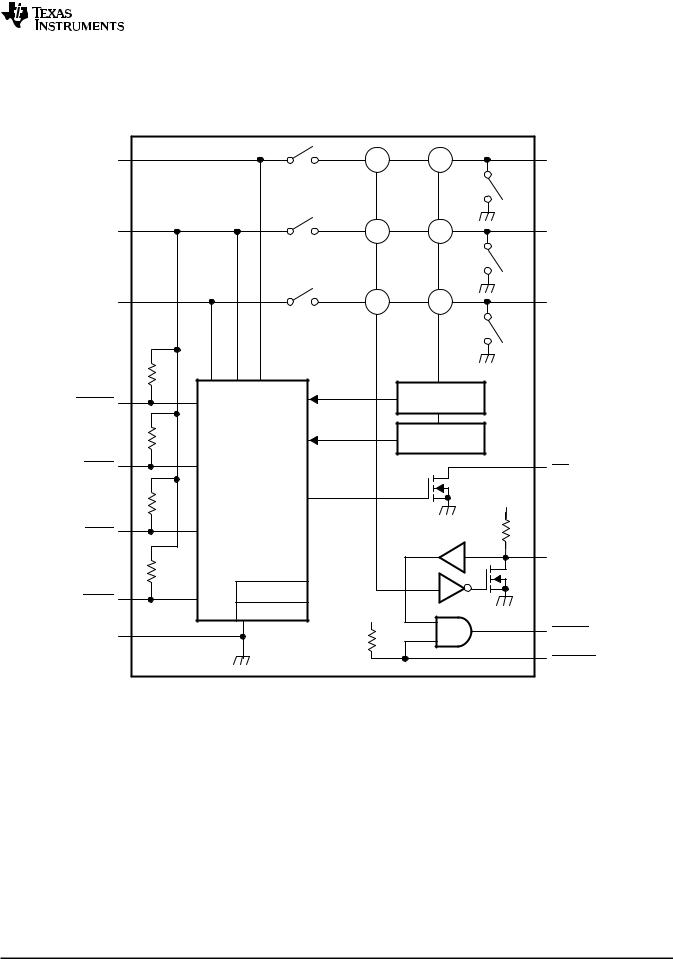
TPS2231
TPS2236
www.ti.com |
SLVS536J –JULY 2004 –REVISED SEPTEMBER 2009 |
FUNCTIONAL BLOCK DIAGRAM
Single ExpressCard Power Switch
3.3VIN |
|
PG |
CS |
|
3.3VOUT |
|
S1 |
(Note A) |
(Note B) |
|
|
|
|
S4 |
|
||
|
|
|
|
|
|
AUXIN |
|
PG |
CS |
|
AUXOUT |
|
S2 |
|
|
|
|
|
|
|
|
S5 |
|
1.5VIN |
|
PG |
CS |
|
1.5VOUT |
|
S3 |
|
|
|
|
|
|
|
|
S6 |
|
CPUSB |
|
|
Current Limit |
|
|
|
|
|
|
|
|
|
|
|
Thermal Limit |
|
|
CPPE |
|
|
|
|
OC |
|
|
|
|
|
|
Control |
|
FAULT |
|
AUXIN |
|
Logic |
|
ALL |
|
|
|
|
|
|
|
||
STBY |
|
|
|
|
|
|
GOOD |
Delay |
|
RCLKEN |
|
|
|
|
|||
|
|
|
|
|
|
UVLO |
|
PWR_ |
|
|
|
SHDN |
|
|
|
|
|
POR |
|
AUXIN |
|
|
|
|
|
|
|
|
|
GND |
PERST |
|
(Note C) |
||
|
||
|
SYSRST |
Note A: PG = power good
Note B: CS = current sense
Note C: TPS2231MRGP-2 does not have a pull-up resistor.
Copyright © 2004–2009, Texas Instruments Incorporated |
Submit Documentation Feedback |
9 |
Product Folder Link(s): TPS2231 TPS2236

TPS2231
TPS2236
SLVS536J –JULY 2004 –REVISED SEPTEMBER 2009 |
www.ti.com |
Dual ExpressCard Power Switch
3.3VIN |
PG1 |
|
CS |
3.3VOUT1 |
|
S1 |
|
|
|
|
|
|
S4 |
|
AUXIN |
PG1 |
|
CS |
AUXOUT1 |
|
S2 |
|
|
|
|
|
|
S5 |
|
1.5VIN |
PG1 |
|
CS |
1.5 VOUT1 |
|
S3 |
|
|
|
|
|
|
S6 |
|
|
PG2 |
|
CS |
3.3VOUT2 |
|
S7 |
|
|
|
|
|
|
S10 |
|
|
PG2 |
|
CS |
AUXOUT2 |
|
S8 |
|
|
|
|
|
|
S11 |
|
|
PG2 |
|
CS |
1.5VOUT2 |
|
S9 |
|
|
|
|
|
|
S12 |
|
CPUSB1 |
|
|
Current Limit |
|
|
|
|
Thermal Limit |
|
CPPE1 |
|
|
|
OC1 |
|
|
|
CHANNEL-1 |
|
|
|
|
AUXIN |
|
|
|
|
FAULT |
|
STBY1 |
|
1 |
|
|
|
|
ALL |
Delay |
|
|
|
|
|
|
|
|
GOOD |
|
RCLKEN1 |
SHDN1 |
Control |
|
|
|
|
Logic |
_ |
|
|
|
PWR |
|
|
|
|
|
|
|
|
CPUSB2 |
2 |
|
|
PERST1 |
|
ALL |
|
|
|
|
|
|
SYSRST |
|
|
GOOD |
|
|
|
CPPE2 |
|
Delay |
RCLKEN2 |
|
|
|
|
||
|
|
|
|
|
STBY2 |
PWR |
|
|
|
|
|
|
|
|
|
UVLO |
|
|
PERST2 |
|
|
|
|
|
SHDN2 |
POR |
|
CHANNEL-2 |
OC2 |
|
|
|||
|
|
|
|
|
GND |
|
|
FAULT |
|
|
|
|
|
10 |
Submit Documentation Feedback |
Copyright © 2004–2009, Texas Instruments Incorporated |
Product Folder Link(s): TPS2231 TPS2236
TPS2231
TPS2236
www.ti.com |
SLVS536J –JULY 2004 –REVISED SEPTEMBER 2009 |
DETAILED PIN DESCRIPTIONS
CPPE
A logic low level on this input indicates that the card present supports PCI Express functions. CPPE connects to the AUXIN input through an internal pullup. When a card is inserted, CPPE is physically connected to ground if the card supports PCI Express functions.
CPUSB
A logic low level on this input indicates that the card present supports USB functions. CPUSB connects to the AUXIN input through an internal pullup. When a card is inserted, CPUSB is physically connected to ground if the card supports USB functions.
SHDN
When asserted (logic low), this input instructs the power switch to turn off all voltage outputs and the discharge FETs are activated. SHDN has an internal pullup connected to AUXIN.
STBY
When asserted (logic low) after the card is inserted, this input places the power switch in standby mode by turning off the 3.3-V and 1.5-V power switches and keeping the AUX switch on. If asserted prior to the card being present, STBY places the power switch in OFF Mode by turning off the AUX, 3.3-V, and 1.5-V power switches. STBY has an internal pullup connected to AUXIN.
RCLKEN
This pin serves as both an input and an output. On power up, a discharge FET keeps this signal at a low state as long as any of the output power rails are out of their tolerance range. Once all output power rails are within tolerance, the switch releases RCLKEN allowing it to transition to a high state (internally pulled up to AUXIN). The transition of RCLKEN from a low to a high state starts an internal timer for the purpose of deasserting PERST. As an input, RCLKEN can be kept low to delay the start of the PERST internal timer.
Because RCLKEN is internally connected to a discharge FET, this pin can only be driven low and should never be driven high as a logic input. When an external circuit drives this pin low, RCLKEN becomes an input; otherwise, this pin is an output.
RCLKEN can be used by the host system to enable a clock driver.
PERST
On power up, this output remains asserted (logic level low) until all power rails are within tolerance. Once all power rails are within tolerance and RCLKEN has been released (logic high), PERST is deasserted (logic high) after a time delay as shown in the parametric table. On power down, this output is asserted whenever any of the power rails drop below their voltage tolerance.
The PERST signal is an output from the host system and an input to the ExpressCard module. This signal is only used by PCI Express-based modules and its function is to place the ExpressCard module in a reset state.
During power up, power down, or whenever power to the ExpressCard module is not stable or not within voltage tolerance limits, the ExpressCard standard requires that PERST be asserted. As a result, this signal also serves as a power-good indicator to the ExpressCard module, and the relationship between the power rails and PERST are explicitly defined in the ExpressCard standard.
The host can also place the ExpressCard module in a reset state by asserting a system reset SYSRST. This system reset generates a PERST to the ExpressCard module without disrupting the voltage rails. This is what is normally called a warm reset. However, in a cold start situation, the system reset can also be used to extend the length of time that PERST is asserted.
Copyright © 2004–2009, Texas Instruments Incorporated |
Submit Documentation Feedback |
11 |
Product Folder Link(s): TPS2231 TPS2236

TPS2231
TPS2236
SLVS536J –JULY 2004 –REVISED SEPTEMBER 2009 |
www.ti.com |
SYSRST
This input is driven by the host system and directly affects PERST. Asserting SYSRST (logic low) forces PERST to assert. RCLKEN is not affected by the assertion of SYSRST. SYSRST has an internal pullup connected to AUXIN.
OC
This pin is an open-drain output. When any of the three power switches (AUX, 3.3V, and 1.5V) is in an overcurrent condition, OC is asserted (logic low) by an internal discharge FET with a deglitch delay. Otherwise, the discharge FET is open, and the pin can be pulled up to a power supply through an external resistor.
FUNCTIONAL TRUTH TABLES
Truth Table for Voltage Outputs
VOLTAGE INPUTS (1) |
|
|
|
LOGIC INPUTS |
|
|
VOLTAGE OUTPUTS (2) |
MODE (3) |
||||||||
AUXIN |
3.3VIN |
1.5VIN |
|
SHDN |
|
|
|
STBY |
|
|
CP |
(4) |
AUXOUT |
3.3VOUT |
1.5VOUT |
|
Off |
x |
x |
|
x |
|
|
x |
|
x |
Off |
Off |
Off |
OFF |
|||
|
|
|
|
|
|
|
|
|
|
|
|
|
|
|
|
|
On |
x |
x |
0 |
|
|
|
x |
|
x |
GND |
GND |
GND |
Shutdown |
|||
|
|
|
|
|
|
|
|
|
|
|
|
|
|
|
|
|
On |
x |
x |
1 |
|
|
|
x |
|
1 |
GND |
GND |
GND |
No Card |
|||
|
|
|
|
|
|
|
|
|
|
|
|
|
|
|
|
|
On |
On |
On |
1 |
|
|
0 |
|
|
0 |
On |
Off |
Off |
Standby |
|||
|
|
|
|
|
|
|
|
|
|
|
|
|
|
|
|
|
On |
On |
On |
1 |
|
|
1 |
|
|
0 |
On |
On |
On |
Card Inserted |
|||
|
|
|
|
|
|
|
|
|
|
|
|
|
|
|
|
|
(1)For input voltages, On means the respective input voltage is higher than its turnon threshold voltage; otherwise, the voltage is Off (for AUX input,Off means the voltage is close to zero volt).
(2)For output voltages, On means the respective power switch is turned on so the input voltage is connected to the output; Off means the power switch and its output discharge FET are both off; GND means the power switch is off but the output discharge FET is on so the voltage on the output is pulled down to 0 V.
(3)Mode assigns each set of input conditions and respective output voltage results to a different name. These modes are referred to as input conditions in the following Truth Table for Logic Outputs.
(4)CP = CPUSB and CPPE – equal to 1 when both CPUSB and CPPE signals are logic high, or equal to 0 when either CPUSB or CPPE is low.
Truth Table for Logic Outputs
|
INPUT CONDITIONS |
|
|
|
|
LOGIC OUTPUTS |
|||
|
|
|
|
|
|
|
|
|
|
MODE |
|
SYSRST |
|
RCLKEN (1) |
|
PERST |
|
|
RCLKEN (2) |
OFF |
|
|
|
|
|
|
|
|
|
|
|
|
|
|
|
|
|
|
|
Shutdown |
|
X |
X |
0 |
|
|
0 |
||
|
|
|
|
||||||
No Card |
|
||||||||
|
|
|
|
|
|
|
|
|
|
|
|
|
|
|
|
|
|
|
|
Standby |
|
|
|
|
|
|
|
|
|
|
|
|
|
|
|
|
|
|
|
|
0 |
|
Hi-Z |
0 |
|
|
1 |
||
|
|
|
|
|
|
|
|
|
|
Card Inserted |
0 |
|
0 |
0 |
|
|
0 |
||
|
|
|
|
|
|
|
|
|
|
1 |
|
Hi-Z |
1 |
|
|
1 |
|||
|
|
|
|
||||||
|
|
|
|
|
|
|
|
|
|
|
1 |
|
0 |
0 |
|
|
0 |
||
|
|
|
|
|
|
|
|
|
|
(1)RCLKEN as a logic input in this column. RCLKEN is an I/O pin and it can be driven low externally, left open, or connected to high-impedance terminals, such as the gate of a MOSFET. It must not be driven high externally.
(2)RCLKEN as a logic output in this column.
12 |
Submit Documentation Feedback |
Copyright © 2004–2009, Texas Instruments Incorporated |
Product Folder Link(s): TPS2231 TPS2236

TPS2231
TPS2236
www.ti.com |
SLVS536J –JULY 2004 –REVISED SEPTEMBER 2009 |
POWER STATES
If AUXIN is not present, then all input-to-output power switches are kept off (OFF mode).
If AUXIN is present and SHDN is asserted (logic low), then all input-to-output power switches are kept off and the output discharge FETs are turned on (Shutdown mode). If SHDN is asserted and then de-asserted, the state on the outputs is restored to the state prior to SHDN assertion.
If 3.3VIN, AUXIN and 1.5VIN are present at the input of the power switch and no card is inserted, then all input-to-output power switches are kept off and the output discharge FETs are turned on (No Card mode).
If 3.3VIN, AUXIN and 1.5VIN are present at the input of the power switch prior to a card being inserted, then all input-to-output power switches are turned on once a card-present signal (CPUSB and/or CPPE) is detected (Card Inserted mode).
If a card is present and all output voltages are being applied, then the STBY is asserted (logic low); the AUXOUT voltage is provided to the card, and the 3.3VOUT and 1.5VOUT switches are turned off (Standby mode).
If a card is present and all output voltages are being applied, then the 1.5VIN, or 3.3VIN is removed from the input of the power switch; the AUXOUT voltage is provided to the card and the 3.3VOUT and 1.5VOUT switches are turned off (Standby mode). TPS2231-3 only: If 3.3VIN is removed, the 3.3VOUT switch is turned off; and, the 1.5VOUT switch is unaffected. If 1.5VIN is removed, the 1.5VOUT switch is turned off; and, the 3.3VOUT switch is unaffected.
If prior to the insertion of a card, the AUXIN is available at the input of the power switch and 3.3VIN and/or 1.5VIN are not, or if STBY is asserted (logic low), then no power is made available to the card (OFF mode). If 1.5VIN and 3.3VIN are made available at the input of the power switch after the card is inserted and STBY is not asserted, all the output voltages are made available to the card (Card Inserted mode). TPS2231-3 only: If 1.5VIN or 3.3VIN is made available at the input of the power switch after the card is inserted and STBY is not asserted, all switches above their individual UVLO thresholds will turn on.
DISCHARGE FETs
The discharge FETs on the outputs are activated whenever the device detects that a card is not present (No Card mode). Activation occurs after the input-to-output power switches are turned off (break before make). The discharge FETs de-activate if either of the card-present lines go active low, unless the SHDN pin is asserted.
The discharge FETs are also activated whenever the SHDN input is asserted and stay asserted until SHDN is de-asserted.
Copyright © 2004–2009, Texas Instruments Incorporated |
Submit Documentation Feedback |
13 |
Product Folder Link(s): TPS2231 TPS2236
Loading...