


 Loading...
Texas Instruments TPS61030PWP, TPS61030RSAR, TPS61031PWP, TPS61031RSAR, TPS61032PWP Schematic [ru]
...PRODUCT |
SAMPLE & |
TECHNICAL |
TOOLS & |
SUPPORT & |
FOLDER |
BUY |
DOCUMENTS |
SOFTWARE |
COMMUNITY |
TPS61030, TPS61031, TPS61032
SLUS534G –SEPTEMBER 2002–REVISED MARCH 2015
TPS6103x 96% Efficient Synchronous Boost Converter With 4A Switch
1 Features
•96% Efficient Synchronous Boost Converter With
1000-mA Output Current From 1.8-V Input
•Device Quiescent Current: 20-µA (Typ)
•Input Voltage Range: 1.8-V to 5.5-V
•Fixed and Adjustable Output Voltage Options Up to 5.5-V
•Power Save Mode for Improved Efficiency at Low Output Power
•Low Battery Comparator
•Low EMI-Converter (Integrated Antiringing Switch)
•Load Disconnect During Shutdown
•Over-Temperature Protection
•Available in a Small 4 mm x 4 mm QFN-16 or in a TSSOP-16 Package
2 Applications
All Single Cell Li or Dual Cell Battery Operated
Products as MP-3 Player, PDAs, and Other
Portable Equipment
3 Description
The TPS6103x devices provide a power supply solution for products powered by either a one-cell LiIon or Li-polymer, or a two to three-cell alkaline, NiCd or NiMH battery. The converter generates a stable output voltage that is either adjusted by an external resistor divider or fixed internally on the chip. It provides high efficient power conversion and is capable of delivering output currents up to 1 A at 5 V at a supply voltage down to 1.8 V. The implemented boost converter is based on a fixed frequency, pulsewidthmodulation (PWM) controller using a synchronous rectifier to obtain maximum efficiency. At low load currents the converter enters Power Save mode to maintain a high efficiency over a wide load current range. The Power Save mode can be disabled, forcing the converter to operate at a fixed switching frequency. It can also operate synchronized to an external clock signal that is applied to the SYNC pin. The maximum peak current in the boost switch is limited to a value of 4500 mA.
The converter can be disabled to minimize battery drain. During shutdown, the load is completely disconnected from the battery. A low-EMI mode is implemented to reduce ringing and, in effect, lower radiated electromagnetic energy when the converter enters the discontinuous conduction mode.
Device Information(1)
PART NUMBER |
PACKAGE |
BODY SIZE (NOM) |
TPS61030 |
|
|
TPS61031 |
TSSOP (16) |
5.00 mm × 4.40 mm |
TPS61032 |
|
|
TPS61030 |
|
|
TPS61031 |
QFN (16) |
4.00 mm x 4.00 mm |
TPS61032 |
|
|
(1) For all available packages, see the orderable addendum at the end of the datasheet.
4 Simplified Schematic
|
|
L1 |
|
|
|
e.g. 5 V up to |
|
|
|
SW |
VOUT |
|
|
|
|
6.8 µH |
|
1000 mA |
||
|
|
|
|
C2 |
||
|
|
|
|
|
C3 |
|
|
|
|
VBAT |
R3 |
2.2 µF |
220 µF |
1.8 V to 5 V |
C1 |
R1 |
EN |
FB |
|
|
Input |
10 µF |
|
LBI |
R4 |
|
R6 |
|
|
|
|
|||
|
|
R2 |
|
|
|
|
|
|
|
SYNC |
LBO |
|
Low Battery |
|
|
|
|
|
||
|
|
|
GND |
PGND |
|
Comparator |
|
|
|
|
Output |
||
|
|
|
|
|
|
|
|
|
|
|
TPS6103x |
|
|
An IMPORTANT NOTICE at the end of this data sheet addresses availability, warranty, changes, use in safety-critical applications, intellectual property matters and other important disclaimers. PRODUCTION DATA.

TPS61030, TPS61031, TPS61032
SLUS534G –SEPTEMBER 2002 –REVISED MARCH 2015 www.ti.com
Table of Contents
1 |
Features .................................................................. |
1 |
|
10.3 |
Feature Description............................................... |
10 |
||
2 |
Applications ........................................................... |
1 |
|
10.4 |
Device Functional Modes...................................... |
10 |
||
3 |
Description ............................................................. |
1 |
11 |
Application and Implementation........................ |
12 |
|||
4 |
Simplified Schematic............................................. |
1 |
|
11.1 |
Application Information.......................................... |
12 |
||
5 |
Revision History |
2 |
|
11.2 |
Typical Application ............................................... |
12 |
||
12 |
Power Supply Recommendations |
18 |
||||||
6 |
Device Comparison Table |
3 |
||||||
13 |
Layout |
18 |
||||||
7 |
Pin Configuration and Functions |
3 |
||||||
|
13.1 |
Layout Considerations |
18 |
|||||
8 |
Specifications |
4 |
|
|||||
|
13.2 |
Layout Example |
18 |
|||||
|
8.1 |
Absolute Maximum Ratings |
4 |
|
||||
|
|
13.3 |
Thermal Considerations |
18 |
||||
|
8.2 |
ESD Ratings |
4 |
|
||||
|
14 Device and Documentation Support |
19 |
||||||
|
8.3 |
Recommended Operating Conditions |
4 |
|||||
|
|
14.1 |
Device Support |
19 |
||||
|
8.4 |
Thermal Information |
4 |
|
||||
|
|
14.2 |
Related Links |
19 |
||||
|
8.5 |
Electrical Characteristics |
5 |
|
||||
|
|
14.3 |
Trademarks |
19 |
||||
|
8.6 |
Typical Characteristics |
6 |
|
||||
|
|
14.4 |
Electrostatic Discharge Caution |
19 |
||||
9 |
Parameter Measurement Information |
8 |
|
|||||
|
14.5 |
Glossary |
19 |
|||||
10 |
Detailed Description |
9 |
|
|||||
15 Mechanical, Packaging, and Orderable |
|
|||||||
|
10.1 |
Overview |
9 |
|
||||
|
|
Information |
19 |
|||||
|
10.2 |
Functional Block Diagram |
9 |
|
||||
|
|
|
|
|
||||
|
|
|
|
|
|
|
|
|
5 |
Revision History |
|
NOTE: Page numbers for previous revisions may differ from page numbers in the current version. |
|
|
Changes from Revision F (October 2014) to Revision G |
Page |
|
|
|
|
• Moved Tstg spec to the Absolute Maximum Ratings table. Changed Handling Ratings to ESD Ratings |
............................... 4 |
|
• |
Added System Examples .................................................................................................................................................... |
16 |
|
|
|
Changes from Revision E (January 2012) to Revision F |
Page |
|
|
|
|
•Added Device Information and Handling Rating tables, Feature Description section, Device Functional Modes, Application and Implementation section, Power Supply Recommendations section, Layout section, Device and
Documentation Support section, and Mechanical, Packaging, and Orderable Information section |
..................................... 1 |
Changes from Revision D (April 2004) to Revision E |
Page |
• Changed the temperature range From: 40°C to 85°C To: -40°C to 85°C.............................................................................. |
3 |
2 |
Submit Documentation Feedback |
Copyright © 2002–2015, Texas Instruments Incorporated |
Product Folder Links: TPS61030 TPS61031 TPS61032
|
|
|
|
TPS61030, TPS61031, TPS61032 |
www.ti.com |
|
|
SLUS534G –SEPTEMBER 2002 –REVISED MARCH 2015 |
|
6 Device Comparison Table (1) |
|
|
|
|
|
|
|
|
|
TA |
OUTPUT VOLTAGE |
PACKAGE |
|
PART NUMBER(1) |
|
DC/DC |
|
|
|
|
Adjustable |
|
|
TPS61030 |
|
3.3 V |
16-Pin TSSOP PowerPAD™ |
|
TPS61031 |
-40°C to 85°C |
5 V |
|
|
TPS61032 |
Adjustable |
|
|
TPS61030 |
|
|
|
|
||
|
3.3 V |
16-Pin QFN |
|
TPS61031 |
|
5 V |
|
|
TPS61032 |
(1)Contact the factory to check availability of other fixed output voltage versions.
(1)For all available packages, see the orderable addendum at the end of the datasheet.
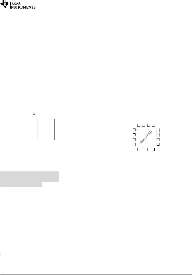
7 Pin Configuration and Functions
|
|
|
|
PWP Package |
|
|
|
|
|
|
|
|
16-Pins |
|
|
|
|
|
|
|
|
Top View |
|
|
|
|
|
|
|
|
|
|
|
|
|
SW |
|
|
1 |
|
16 |
|
|
NC |
|
|
|
|
|
||||
SW |
|
|
2 |
|
15 |
|
|
|
|
|
|
|
|
VOUT |
|||
|
|
|
|
|
||||
|
|
|
3 |
|
14 |
|
|
|
|
|
|
|
|
|
|||
PGND |
|
|
|
|
|
VOUT |
||
PGND |
|
|
4 |
|
13 |
|
|
|
|
|
POWERPAD |
|
|
VOUT |
|||
|
|
|
|
|||||
PGND |
|
|
5 |
12 |
|
|
||
|
|
|
|
FB |
||||
|
|
|
|
|
||||
|
|
|
6 |
|
11 |
|
|
|
|
|
|
|
|
||||
VBAT |
|
|
|
|
|
GND |
||
|
|
|
7 |
|
10 |
|
|
|
|
|
|
|
|
||||
LBI |
|
|
|
|
|
LBO |
||
|
|
|
8 |
|
9 |
|
|
|
|
|
|
|
|
||||
SYNC |
|
|
|
|
|
EN |
||
|
|
|
|
|
|
|
|
|
|
|
|
|
|
|
|
|
|
NC − NO INTERNAL CONNECTION |
|
|
|
|
||||
Pin Functions
RSA Package
16-Pins
Top View
|
|
VOUT |
|
|
|
VOUT |
|
FB GND |
||||||||||||||||||||
|
|
|
|
|
|
|
|
|
|
|
|
|
|
|
|
|
|
|
|
|
|
|
|
|
|
|
|
|
VOUT |
|
|
|
|
|
|
|
|
|
|
|
|
|
|
|
|
|
|
|
|
|
|
|
|
|
|
|
|
|
|
|
|
|
|
|
|
|
|
|
|
|
|
|
|
|
|
|
|
|
|
|
|
|
|
|
|
|
|
|
|
|
|
|
|
|
|
|
|
|
|
|
|
|
|
|
|
|
|
|
|
|
|
|
|
|
|
|
|
|
|
|
|
|
|
|
|
|
|
|
|
|
|
|
|
|
|
|
|
|
|
|
|
|
|
|
NC |
|
|
|
|
|
|
|
|
|
|
|
|
|
|
|
|
|
|
|
|
|
|
|
|
|
|
|
|
|
|
|
|
|
|
|
|
|
|
|
|
|
|
|
|
|
|
|
|
|
|
|
|
|
|
|
|
|
SW |
|
|
|
|
|
|
|
|
|
|
|
|
|
|
|
|
|
|
|
|
|
|
|
|
|
|
|
|
|
|
|
|
|
|
|
|
|
|
|
|
|
|
|
|
|
|
|
|
|
|
|
|
|
|
|
|
|
SW |
|
|
|
|
|
|
|
|
|
|
|
|
|
|
|
|
|
|
|
|
|
|
|
|
|
|
|
|
|
|
|
|
|
|
|
|
|
|
|
|
|
|
|
|
|
|
|
|
|
|
|
|
|
|
|
|
|
|
|
|
|
|
|
|
|
|
|
|
|
|
|
|
|
|
|
|
|
|
|
|
|
|
|
|
|
|
|
|
|
|
|
|
|
|
|
|
|
|
|
|
|
|
|
|
|
|
|
|
|
|
|
|
|
|
|
|
|
|
|
|
|
|
|
|
|
|
|
|
|
|
|
|
|
|
|
|
|
|
|
|
|
|
|
|
|
|
PGND |
|
|
|
PGND |
|
|
|
PGND VBAT |
||||||||||||||||||
LBO
EN SYNC LBI
|
PIN |
|
|
|
|
|
NAME |
NO. |
|
|
I/O |
DESCRIPTION |
|
PWP |
|
RSA |
|
|
||
|
|
|
|
|||
EN |
9 |
|
11 |
|
I |
Enable input. (1/VBAT enabled, 0/GND disabled) |
FB |
12 |
|
14 |
|
I |
Voltage feedback of adjustable versions |
GND |
11 |
|
13 |
|
I/O |
Control/logic ground |
LBI |
7 |
|
9 |
|
I |
Low battery comparator input (comparator enabled with EN) |
LBO |
10 |
|
12 |
|
O |
Low battery comparator output (open drain) |
NC |
16 |
|
2 |
|
|
Not connected |
PGND |
3, 4, 5 |
|
5, 6, |
7 |
I/O |
Power ground |
PowerPAD™ |
|
|
|
|
|
Must be soldered to achieve appropriate power dissipation. Should be connected to |
|
|
|
|
|
|
PGND. |
SYNC |
8 |
|
10 |
|
I |
Enable/disable power save mode (1/VBAT disabled, 0/GND enabled, clock signal for |
|
|
|
|
|
|
synchronization) |
SW |
1, 2 |
|
3, 4 |
|
I |
Boost and rectifying switch input |
VBAT |
6 |
|
8 |
|
I |
Supply voltage |
VOUT |
13, 14, 15 |
|
1, 15, |
16 |
O |
DC/DC output |
Copyright © 2002–2015, Texas Instruments Incorporated |
Submit Documentation Feedback |
3 |
Product Folder Links: TPS61030 TPS61031 TPS61032

TPS61030, TPS61031, TPS61032
SLUS534G –SEPTEMBER 2002 –REVISED MARCH 2015 |
www.ti.com |
8 Specifications
8.1 Absolute Maximum Ratings
over operating free-air temperature range (unless otherwise noted)(1)
|
|
MIN |
MAX |
UNIT |
|
VI |
Input voltage on LBI |
–0.3 |
3.6 |
V |
|
|
Input voltage on SW, VOUT, LBO, VBAT, SYNC, EN, FB |
–0.3 |
7 |
V |
|
TJ |
Maximum junction temperature |
–40 |
150 |
°C |
|
Tstg |
Storage temperature range |
–65 |
150 |
||
|
(1)Stresses beyond those listed under Absolute Maximum Ratings may cause permanent damage to the device. These are stress ratings only, and functional operation of the device at these or any other conditions beyond those indicated under Recommended Operating Conditions is not implied. Exposure to absolute-maximum-rated conditions for extended periods may affect device reliability.
8.2 |
ESD Ratings |
|
|
|
||
|
|
|
|
MIN |
MAX |
UNIT |
|
|
|
Human body model (HBM), per ANSI/ESDA/JEDEC JS-001, all |
–2000 |
2000 |
|
V(ESD) |
|
Electrostatic discharge |
pins(1) |
|
|
V |
|
Charged device model (CDM), per JEDEC specification JESD22- |
–1000 |
1000 |
|||
|
|
|
C101, all pins(2) |
|
|
|
(1)JEDEC document JEP155 states that 500-V HBM allows safe manufacturing with a standard ESD control process.
(2)JEDEC document JEP157 states that 250-V CDM allows safe manufacturing with a standard ESD control process.
8.3 |
Recommended Operating Conditions |
|
|
|
|
|
MIN |
NOM MAX |
UNIT |
VI |
Supply voltage at VBAT |
1.8 |
5.5 |
V |
TA |
Operating ambient temperature range |
-40 |
85 |
°C |
TJ |
Operating virtual junction temperature range |
-40 |
125 |
°C |
8.4 Thermal Information
|
|
TPS6103x |
|
||
|
THERMAL METRIC(1) |
PWP |
RSA |
UNIT |
|
|
|
16 PINS |
16 PINS |
|
|
RθJA |
Junction-to-ambient thermal resistance |
46.9 |
35.5 |
|
|
RθJC(top) |
Junction-to-case (top) thermal resistance |
25.8 |
36.7 |
|
|
RθJB |
Junction-to-board thermal resistance |
19.4 |
12.9 |
°C/W |
|
ψJT |
Junction-to-top characterization parameter |
0.8 |
0.5 |
||
|
|||||
ψJB |
Junction-to-board characterization parameter |
19.3 |
12.9 |
|
|
RθJC(bot) |
Junction-to-case (bottom) thermal resistance |
2.2 |
3.8 |
|
|
(1)For more information about traditional and new thermal metrics, see the IC Package Thermal Metrics application report, SPRA953.
4 |
Submit Documentation Feedback |
Copyright © 2002–2015, Texas Instruments Incorporated |
Product Folder Links: TPS61030 TPS61031 TPS61032

TPS61030, TPS61031, TPS61032
www.ti.com |
SLUS534G –SEPTEMBER 2002 –REVISED MARCH 2015 |
8.5 Electrical Characteristics
over recommended free-air temperature range and over recommended input voltage range (typical at an ambient temperature range of 25°C) (unless otherwise noted)
|
PARAMETER |
TEST CONDITIONS |
MIN |
TYP |
MAX |
UNIT |
|
DC/DC STAGE |
|
|
|
|
|
||
VI |
Input voltage range |
|
1.8 |
|
5.5 |
V |
|
VO |
TPS61030 output voltage range |
|
1.8 |
|
5.5 |
V |
|
VFB |
TPS61030 feedback voltage |
|
490 |
500 |
510 |
mV |
|
f |
Oscillator frequency |
|
500 |
600 |
700 |
kHz |
|
|
Frequency range for synchronization |
|
500 |
|
700 |
kHz |
|
|
Switch current limit |
VOUT= 5 V |
3600 |
4000 |
4500 |
mA |
|
|
Start-up current limit |
|
|
0.4 x ISW |
|
mA |
|
|
SWN switch on resistance |
VOUT= 5 V |
|
55 |
|
mΩ |
|
|
SWP switch on resistance |
VOUT= 5 V |
|
55 |
|
mΩ |
|
|
Total accuracy |
|
-3% |
|
3% |
|
|
|
Line regulation |
|
|
|
0.6% |
|
|
|
Load regulation |
|
|
|
0.6% |
|
|
|
|
VBAT |
IO = 0 mA, VEN = VBAT = 1.8 V, |
|
10 |
25 |
µA |
|
Quiescent current |
|
VOUT =5 V |
|
|
|
|
|
VOUT |
IO = 0 mA, VEN = VBAT = 1.8 V, |
|
10 |
20 |
µA |
|
|
|
|
|||||
|
|
|
VOUT = 5 V |
|
|
|
|
|
Shutdown current |
|
VEN= 0 V, VBAT = 2.4 V |
|
0.1 |
1 |
µA |
CONTROL STAGE |
|
|
|
|
|
||
VUVLO |
Under voltage lockout threshold |
VLBI voltage decreasing |
|
1.5 |
|
V |
|
VIL |
LBI voltage threshold |
VLBI voltage decreasing |
490 |
500 |
510 |
mV |
|
|
LBI input hysteresis |
|
|
10 |
|
mV |
|
|
LBI input current |
EN = VBAT or GND |
|
0.01 |
0.1 |
µA |
|
|
LBO output low voltage |
VO = 3.3 V, IOI = 100 µA |
|
0.04 |
0.4 |
V |
|
|
LBO output low current |
|
|
100 |
|
µA |
|
|
LBO output leakage current |
VLBO= 7 V |
|
0.01 |
0.1 |
µA |
|
VIL |
EN, SYNC input low voltage |
|
|
|
0.2 × VBAT |
V |
|
VIH |
EN, SYNC input high voltage |
|
0.8 × VBAT |
|
|
V |
|
|
EN, SYNC input current |
Clamped on GND or VBAT |
|
0.01 |
0.1 |
µA |
|
|
Overtemperature protection |
|
|
140 |
|
°C |
|
|
Overtemperature hysteresis |
|
|
20 |
|
°C |
|
Copyright © 2002–2015, Texas Instruments Incorporated |
Submit Documentation Feedback |
5 |
Product Folder Links: TPS61030 TPS61031 TPS61032

TPS61030, TPS61031, TPS61032
SLUS534G –SEPTEMBER 2002 –REVISED MARCH 2015 www.ti.com
8.6 Typical Characteristics
Table 1. Table Of Graphs
DC/DC CONVERTER |
|
FIGURE |
|
Maximum output current |
vs Input voltage |
Figure 1, |
|
Figure 2 |
|||
|
|
||
|
vs Output current (TPS61030) (VO = 2.5 V, VI = 1.8 V, VSYNC = 0 V) |
Figure 3 |
|
|
vs Output current (TPS61031) (VO = 3.3 V, VI = 1.8 V, 2.4 V, VSYNC = 0 V) |
Figure 4 |
|
Efficiency |
vs Output current (TPS61032) (VO = 5.0 V, VI = 2.4 V, 3.3 V, VSYNC = 0 V) |
Figure 5 |
|
|
vs Input voltage (TPS61031) (IO = 10 mA, 100 mA, 1000 mA, VSYNC = 0 V) |
Figure 6 |
|
|
vs Input voltage (TPS61032) (IO = 10 mA, 100 mA, 1000 mA, VSYNC = 0 V) |
Figure 7 |
|
Output voltage |
vs Output current (TPS61031) (VI = 2.4 V) |
Figure 8 |
|
vs Output current (TPS61032) (VI = 3.3 V) |
Figure 9 |
||
|
|||
No-load supply current into VBAT |
vs Input voltage (TPS61032) |
Figure 10 |
|
No-load supply current into VOUT |
vs Input voltage (TPS61032) |
Figure 11 |
|
Minimum Load Resistance at |
vs Input voltage (TPS61032) |
Figure 12 |
|
Startup |
|||
|
|
Maximum Output Current - A
3.5 |
|
|
|
|
|
|
|
|
|
|
3.5 |
|
|
|
|
|
|
|
|
|
3 |
|
|
|
|
|
|
|
|
|
|
3 |
|
|
|
|
|
|
|
|
|
|
|
|
|
|
|
|
|
|
|
A |
|
|
|
|
|
|
|
|
|
|
2.5 |
|
|
|
|
|
|
|
|
|
- |
2.5 |
|
|
|
|
|
|
|
|
|
|
|
|
|
|
|
|
|
|
Current |
|
|
|
|
|
|
|
|
|
||
2 |
|
|
|
|
|
|
|
|
|
2 |
|
|
|
|
|
|
|
|
|
|
|
|
|
|
|
|
|
|
|
Output |
|
|
|
|
|
|
|
|
|
||
1.5 |
|
|
|
|
|
|
|
|
|
1.5 |
|
|
|
|
|
|
|
|
|
|
|
|
|
|
|
|
|
|
|
Maximum |
|
|
|
|
|
|
|
|
|
||
1 |
|
|
|
|
|
|
|
|
|
1 |
|
|
|
|
|
|
|
|
|
|
0.5 |
|
|
|
|
|
|
|
|
|
|
0.5 |
|
|
|
|
|
|
|
|
|
0 |
1.8 |
2.2 |
2.6 |
3 |
3.4 |
3.8 |
4.2 |
4.6 |
5 |
|
0 |
1.8 |
2.2 |
2.6 |
3 |
3.4 |
3.8 |
4.2 |
4.6 |
5 |
|
|
|
VI - Input Voltage - V |
|
|
|
|
|
|
|
VI - Input Voltage - V |
|
|
|
||||||
Figure 1. TPS61031 Maximum Output Current |
Figure 2. TPS61032 Maximum Output Current |
vs Input Voltage |
vs Input Voltage |
6 |
Submit Documentation Feedback |
Copyright © 2002–2015, Texas Instruments Incorporated |
Product Folder Links: TPS61030 TPS61031 TPS61032

|
|
|
|
|
|
|
|
TPS61030, TPS61031, TPS61032 |
|||
www.ti.com |
|
|
|
|
|
|
|
SLUS534G –SEPTEMBER 2002 –REVISED MARCH 2015 |
|||
|
100 |
|
|
|
|
|
100 |
|
|
|
|
|
90 |
|
|
|
|
|
90 |
|
|
|
|
|
|
|
|
|
|
|
|
VBAT = 1.8 V |
|
|
|
|
80 |
|
|
|
|
|
80 |
|
VBAT |
= 2.4 V |
|
|
|
|
|
|
|
|
|
|
|
||
|
70 |
|
|
|
|
|
70 |
|
|
|
|
% |
60 |
|
|
|
|
% |
60 |
|
|
|
|
- |
|
|
|
|
- |
|
|
|
|
||
|
|
|
|
|
|
|
|
|
|
||
Efficiency |
50 |
|
|
|
|
Efficiency |
50 |
|
|
|
|
40 |
|
|
|
|
40 |
|
|
|
|
||
|
|
|
|
|
|
|
|
|
|
||
|
30 |
|
|
|
|
|
30 |
|
|
|
|
|
20 |
|
|
|
|
|
20 |
|
|
|
|
|
10 |
|
|
|
|
|
10 |
|
|
|
|
|
0 |
|
|
|
|
|
0 |
|
|
|
|
|
|
|
|
|
|
1 |
10 |
100 |
1000 |
10000 |
|
|
1 |
10 |
100 |
1000 |
10000 |
|
|||||
|
|
|
|
|
|
|
|||||
|
|
IO - Output Current - mA |
|
|
|
IO - Output Current - mA |
|
||||
|
VO = 2.5 V |
|
VI = 1.8 V |
|
|
|
VO = 3.3 V |
|
|
|
|
Figure 3. TPS61030 Efficiency vs Output Current |
Figure 4. TPS61031 Efficiency vs Output Current |
|
100 |
|
|
|
|
|
100 |
|
|
|
|
|
|
|
|
90 |
|
|
|
|
|
|
IO = 100 mA |
|
|
|
|
|
|
|
|
|
|
|
|
|
|
|
|
|
|
|
|
|
|
|
|
VBAT = 2.4 V |
|
|
|
|
|
|
|
|
IO = 1000 mA |
|
|
|
80 |
|
VBAT = 3.3 V |
|
|
|
90 |
|
|
|
|
|
||
|
|
|
|
|
|
|
|
|
IO = 10 mA |
|
|
|
|
|
|
70 |
|
|
|
|
|
|
|
|
|
|
|
|
|
|
|
|
|
|
|
|
|
|
|
|
|
|
|
|
% |
60 |
|
|
|
|
% |
80 |
|
|
|
|
|
|
|
- |
|
|
|
|
- |
|
|
|
|
|
|
|
||
Efficiency |
50 |
|
|
|
|
Efficiency |
|
|
|
|
|
|
|
|
40 |
|
|
|
|
70 |
|
|
|
|
|
|
|
||
|
|
|
|
|
|
|
|
|
|
|
|
|
||
|
30 |
|
|
|
|
|
|
|
|
|
|
|
|
|
|
20 |
|
|
|
|
|
60 |
|
|
|
|
|
|
|
|
10 |
|
|
|
|
|
|
|
|
|
|
|
|
|
|
0 |
|
|
|
|
|
50 |
|
|
|
|
|
|
|
|
1 |
10 |
100 |
1000 |
10000 |
|
1.8 |
2 |
2.2 |
2.4 |
2.6 |
2.8 |
3 |
3.2 |
|
|
IO - Output Current - mA |
|
|
|
|
V |
- Input Voltage - V |
|
|
||||
|
VO = 5 V |
|
|
|
|
|
|
|
I |
|
|
|
|
|
|
|
|
|
|
|
|
|
|
|
|
|
|
|
|
Figure 5. Tps61032 Efficiency vs Output Current |
Figure 6. TPS61031 Efficiency vs Input Voltage |
|
100 |
|
|
|
|
|
|
|
|
|
3.4 |
|
|
|
|
|
|
IO = 100 mA |
|
|
|
|
|
|
|
|
|
|
|
|
|
|
95 |
|
|
|
|
|
|
|
|
|
|
|
|
|
|
|
90 |
|
|
|
|
|
|
|
|
|
|
|
|
|
|
|
|
|
IO = 10 mA |
|
|
|
|
|
|
3.35 |
|
|
|
|
|
|
85 |
|
|
|
|
|
|
V |
|
|
|
|
|
||
|
|
|
|
|
|
|
|
|
|
|
|
|
|
||
Efficiency- % |
|
|
|
|
|
|
|
|
|
- |
|
|
|
|
|
80 |
IO = 1000 mA |
|
|
|
|
|
VoltageOutput |
|
|
|
|
|
|||
|
|
|
|
|
|
|
|
|
|
|
|
||||
|
75 |
|
|
|
|
|
|
|
|
|
3.3 |
|
|
|
|
|
70 |
|
|
|
|
|
|
|
|
|
|
|
|
|
|
|
|
|
|
|
|
|
|
|
|
- |
|
|
|
|
|
|
65 |
|
|
|
|
|
|
|
|
O |
|
|
|
|
|
|
|
|
|
|
|
|
|
|
|
|
|
|
|
|
|
|
|
|
|
|
|
|
|
|
|
V |
3.25 |
|
|
|
|
|
|
|
|
|
|
|
|
|
|
|
|
|
|
|
|
|
60 |
|
|
|
|
|
|
|
|
|
|
|
|
|
|
|
55 |
|
|
|
|
|
|
|
|
|
|
|
|
|
|
|
50 |
|
|
|
|
|
|
|
|
|
3.2 |
|
|
|
|
|
1.8 |
2.2 |
2.6 |
3 |
3.4 |
3.8 |
4.2 |
4.6 |
5 |
|
1 |
10 |
100 |
1000 |
10000 |
|
|
|
VI - Input Voltage - V |
|
|
|
|
|
IO - Output Current - mA |
|
|||||
VBAT = 2.4 V
Figure 7. TPS61032 Efficiency vs Input Voltage |
Figure 8. TPS61031 Output Voltage vs Output Current |
Copyright © 2002–2015, Texas Instruments Incorporated |
Submit Documentation Feedback |
7 |
Product Folder Links: TPS61030 TPS61031 TPS61032

TPS61030, TPS61031, TPS61032 |
|
|
|
|
|
|
|||
SLUS534G –SEPTEMBER 2002 –REVISED MARCH 2015 |
|
|
|
|
www.ti.com |
||||
|
5.2 |
|
|
|
|
16 |
|
|
|
|
5.15 |
|
|
|
µA |
14 |
|
|
85°C |
|
|
|
|
|
|
|
|
|
|
|
|
|
|
|
- |
|
|
|
|
V- |
5.1 |
|
|
|
VBAT |
12 |
|
|
25°C |
|
|
|
|
|
|
||||
VoltageOutput |
4.95 |
|
|
|
IntoCurrent |
6 |
|
|
–40°C |
|
5.05 |
|
|
|
|
10 |
|
|
|
|
|
|
|
|
|
|
|
|
|
|
5 |
|
|
|
|
8 |
|
|
|
|
|
|
|
SupplyLoad-No |
|
|
|
|
|
V |
|
|
|
|
|
|
|
|
|
- |
|
|
|
|
|
|
|
|
|
O |
|
|
|
|
|
|
|
|
|
|
4.9 |
|
|
|
|
4 |
|
|
|
|
4.85 |
|
|
|
|
2 |
|
|
|
|
4.8 |
|
|
|
|
0 |
3 |
4 |
5 |
|
1 |
10 |
100 |
1000 |
10000 |
2 |
|||
|
|
|
|
|
|||||
|
|
IO - Output Current - mA |
|
|
VI - Input Voltage - V |
|
|||
VBAT = 3.3 V
Figure 9. TPS61032 Output Voltage |
Figure 10. TPS61032 No-Load Supply Current into Vbat |
vs Output Current |
vs input Voltage |
|
14 |
85°C |
|
|
|
14 |
|
|
|
|
|
|
|
|
|
|
|
|
|
|
|
|
|
|
|
|
|
|
|
µA |
12 |
|
|
|
! |
12 |
|
|
|
|
|
|
|
|
VOUT - |
25°C |
|
|
Startup- |
|
|
|
|
|
|
|
|
||
|
|
|
|
|
|
|
|
|
|
|
|
|||
10 |
–40°C |
|
|
10 |
|
|
|
|
|
|
|
|
||
|
|
|
|
|
|
|
|
|
|
|
|
|
||
Supply CurrentInto |
8 |
|
|
|
Load Resistance at |
8 |
|
|
|
|
|
|
|
|
6 |
|
|
|
6 |
|
|
|
|
|
|
|
|
||
4 |
|
|
|
4 |
|
|
|
|
|
|
|
|
||
No-Load |
|
|
|
Minimum |
|
|
|
|
|
|
|
|
||
2 |
|
|
|
2 |
|
|
|
|
|
|
|
|
||
|
|
|
|
|
|
|
|
|
|
|
|
|
||
|
0 |
|
|
|
|
0 |
|
|
|
|
|
|
|
|
|
2 |
3 |
4 |
5 |
|
|
|
|
|
|
|
|
|
|
|
|
1.8 |
2.2 |
2.6 |
3 |
3.4 |
3.8 |
4.2 |
4.6 |
5 |
||||
|
|
VI - Input Voltage - V |
|
|
|
|
V |
- Input Voltage - V |
|
|
|
|||
|
|
|
|
|
|
|
|
I |
|
|
|
|
|
|
Figure 11. TPS61032 No-Load Supply Current Into Vout |
Figure 12. Minimum Load Resistance at Start-Up |
vs Input Voltage |
vs Input Voltage |
9 Parameter Measurement Information
|
|
L1 |
|
|
|
|
|
|
|
|
|
6.8 μH |
SW |
VOUT |
|
|
|
|
|
|
|
|
|
C2 |
|
C3 |
|||
|
|
|
VBAT |
|
|
||||
|
|
|
R3 |
2.2 |
μ |
F |
220 |
μ |
|
|
|
|
|
|
F |
||||
Power |
C1 |
R1 |
EN |
FB |
|
|
|
|
|
Supply |
10 μF |
|
LBI |
R4 |
|
|
|
|
R6 |
|
|
|
|
|
|
|
|||
|
|
R2 |
|
|
|
|
|
|
|
|
|
|
SYNC |
LBO |
|
|
|
|
|
|
|
|
|
|
|
|
|
|
|
List of Components: |
|
GND |
PGND |
|
|
|
|
|
|
|
|
TPS6103x |
|
|
|
|
|
||
U1 = TPS6103xPWP |
|
|
|
|
|
|
|
|
|
|
|
|
|
|
|
|
|
|
|
L1 = Sumida CDRH124–6R8 |
|
|
|
|
|
|
|
|
|
C1, C2 = X7R/X5R Ceramic |
|
|
|
|
|
|
|
|
|
C3 = Low ESR Tantalum |
|
|
|
|
|
|
|
|
|
VCC
Boost Output
Control Output
8 |
Submit Documentation Feedback |
Copyright © 2002–2015, Texas Instruments Incorporated |
Product Folder Links: TPS61030 TPS61031 TPS61032

TPS61030, TPS61031, TPS61032
www.ti.com |
SLUS534G –SEPTEMBER 2002 –REVISED MARCH 2015 |
10 Detailed Description
10.1 Overview
The TPS6103x synchronous step-up converter typically operates at a 600 kHz frequency pulse width modulation (PWM) at moderate to heavy load currents. The converter enters Power Save mode at low load currents to maintain a high efficiency over a wide load. The Power Save mode can also be disabled, forcing the converter to operate at a fixed switching frequency. The TPS6103x family is based on a fixed frequency with multiple feed forward controller topology. Input voltage, output voltage, and voltage drop on the NMOS switch are monitored and forwarded to the regulator. The peak current of the NMOS switch is also sensed to limit the maximum current flowing through the switch and the inductor. It can also operate synchronized to an external clock signal that is applied to the SYNC pin. Additionally, TPS6103x integrated the low-battery detector circuit typically used to supervise the battery voltage and to generate an error flag when the battery voltage drops below a user-set threshold voltage.
10.2 Functional Block Diagram
|
SW |
|
|
Anti- |
VOUT |
VBAT |
|
|
Ringing |
|
|
|
PGND |
|
|
|
|
|
|
PGND |
|
Gate |
|
|
Control |
|
|
PGND |
100 kW |
|
|
|
|
|
|
|
|
|
|
|
|
|
|
|
|
|
|
|
|
|
|
|
|
|
|
|
|
|
|
10 pF |
||||
|
|
|
|
|
|
|
|
|
|
|
|
|
|
|
|
|
|
|
Error Amplifier _ |
|
|
|||||||||||
|
|
|
|
|
|
Regulator |
|
|
|
|
|
|
|
|
|
|
|
|
|
FB |
||||||||||||
|
|
|
|
|
|
|
|
|
|
|
|
|
|
|
|
|
|
|
|
|
|
|
|
|
||||||||
|
|
|
|
|
|
|
|
|
|
|
|
|
|
|
|
|
|
|
|
|
|
|
|
|
|
|||||||
|
|
|
|
|
|
|
|
|
|
|
+ |
|
|
|
|
|
|
|
|
|
|
|||||||||||
|
|
|
|
|
|
|
|
|
|
|
|
|
|
|
|
|
|
|
|
|
|
|
|
|||||||||
|
|
|
|
|
|
|
|
|
|
|
|
|
|
|
|
|
|
|
|
|
|
|
+ |
|
|
|
||||||
|
|
|
|
|
|
|
|
|
|
|
|
|
|
|
|
|
|
|
|
VREF = 0.5 V |
|
|
|
|
||||||||
|
|
|
|
|
|
|
|
|
|
|
|
|
|
|
|
|
|
|
|
|
_ |
|
|
|
||||||||
|
|
|
|
|
|
Control Logic |
|
|
|
|
|
|
|
|
|
|
|
|
|
|
|
|
|
|
|
|
||||||
|
|
|
|
|
|
|
|
|
|
|
|
|
|
|
|
|
|
|
|
|
|
|
|
|
|
|||||||
|
|
|
|
|
|
|
|
|
|
|
|
|
|
|
|
|
|
|
|
Oscillator |
|
|
|
GND |
||||||||
|
|
|
|
|
|
|
|
|
|
|
|
|
|
|
|
|
|
|
|
|
|
|
|
|
||||||||
|
|
|
|
|
|
|
|
|
|
|
|
|
|
|
|
|
|
|
|
|
|
|
|
|
||||||||
|
|
|
|
|
|
|
|
|
|
|
|
|
|
|
|
|
|
|
|
|
|
|
|
|
|
|
|
|
|
|||
EN |
|
|
|
|
|
|
|
|
|
|
|
|
|
|
|
|
|
|
Temperature |
|
|
|
|
|
|
|
|
|
|
|
||
|
|
|
|
|
|
|
|
|
|
|
|
|
|
|
|
|
|
|
|
|
|
|
|
|
|
|
|
|
|
|||
|
|
|
|
|
|
|
|
|
|
|
|
|
|
|
Control |
|
|
|
|
|
|
|
|
|
|
|
||||||
SYNC |
|
|
|
|
|
|
|
|
|
|
|
|
|
|
|
|
|
|
|
|
|
|
|
|
|
|
|
|
|
|||
|
|
|
|
|
|
|
|
|
|
|
|
|
|
|
|
|
|
|
|
|
|
|
|
|
|
|
|
|
||||
GND |
|
|
|
|
|
|
|
+ |
Low Battery Comparator |
|
|
|
|
|
|
|
|
|||||||||||||||
|
|
|
|
|
|
|
|
|
|
|
|
|
|
|
||||||||||||||||||
LBI |
|
|
|
|
|
|
|
|
|
|
|
|
|
|
|
|
|
|
||||||||||||||
|
|
|
|
|
|
|
|
|
|
|
|
|
|
|
|
|
|
|
|
|
|
|
|
|
|
|
|
|
LBO |
|||
|
|
|
|
|
|
|
|
|
|
|
|
_ |
|
|
|
|
|
|
|
|
|
|
|
|
|
|
|
|
|
|
|
|
|
|
|
|
|
|
|
|
|
|
|
|
|
|
|
|
|
|
|
|
|
|
|
|
|
|
|
|
|
|
|||
|
|
|
|
|
|
|
|
|
|
|
|
|
|
|
|
|
|
|
|
|
|
|
|
|
|
|
|
|
|
|
|
|
|
+ |
|
VREF = 0.5 V |
|
|
|
|
|
|
|
|
|||||||||||||||||||||
|
_ |
|
|
|
|
|
|
|
|
|
||||||||||||||||||||||
|
|
|
|
|
|
|
|
|
|
|
|
|
|
|
|
|
|
|
|
|
|
|
|
|
|
|
|
|
|
|
||
|
|
|
|
|
|
|
|
|
|
|
|
|
|
|
|
|
|
|
|
|
|
|
|
|
|
|
|
|
|
|
|
|
|
|
|
|
|
|
GND |
|
|
|
|
|
|
|
|
|
|
|
|
|
|
|
|
|
|
|
|
|
|||||
Copyright © 2002–2015, Texas Instruments Incorporated |
Submit Documentation Feedback |
9 |
Product Folder Links: TPS61030 TPS61031 TPS61032

TPS61030, TPS61031, TPS61032
SLUS534G –SEPTEMBER 2002 –REVISED MARCH 2015 |
www.ti.com |
10.3 Feature Description
10.3.1 Controller Circuit
The controller circuit of the device is based on a fixed frequency multiple feedforward controller topology. Input voltage, output voltage, and voltage drop on the NMOS switch are monitored and forwarded to the regulator. So changes in the operating conditions of the converter directly affect the duty cycle and must not take the indirect and slow way through the control loop and the error amplifier. The control loop, determined by the error amplifier, only has to handle small signal errors. The input for it is the feedback voltage on the FB pin or, at fixed output voltage versions, the voltage on the internal resistor divider. It is compared with the internal reference voltage to generate an accurate and stable output voltage.
The peak current of the NMOS switch is also sensed to limit the maximum current flowing through the switch and the inductor. The typical peak current limit is set to 4000 mA. An internal temperature sensor prevents the device from getting overheated in case of excessive power dissipation.
10.3.2 Synchronous Rectifier
The device integrates an N-channel and a P-channel MOSFET transistor to realize a synchronous rectifier. Because the commonly used discrete Schottky rectifier is replaced with a low RDS(ON) PMOS switch, the power conversion efficiency reaches 96%. To avoid ground shift due to the high currents in the NMOS switch, two separate ground pins are used. The reference for all control functions is the GND pin. The source of the NMOS switch is connected to PGND. Both grounds must be connected on the PCB at only one point close to the GND pin. A special circuit is applied to disconnect the load from the input during shutdown of the converter. In conventional synchronous rectifier circuits, the backgate diode of the high-side PMOS is forward biased in shutdown and allows current flowing from the battery to the output. This device however uses a special circuit which takes the cathode of the backgate diode of the high-side PMOS and disconnects it from the source when the regulator is not enabled (EN = low).
The benefit of this feature for the system design engineer is that the battery is not depleted during shutdown of the converter. No additional components have to be added to the design to make sure that the battery is disconnected from the output of the converter.
10.4 Device Functional Modes
10.4.1 Device Enable
The device is put into operation when EN is set high. It is put into a shutdown mode when EN is set to GND. In shutdown mode, the regulator stops switching, all internal control circuitry including the low-battery comparator is switched off, and the load is isolated from the input (as described in the Synchronous Rectifier Section). This also means that the output voltage can drop below the input voltage during shutdown. During start-up of the converter, the duty cycle and the peak current are limited in order to avoid high peak currents drawn from the battery.
10.4.1.1 Undervoltage Lockout
An undervoltage lockout function prevents device start-up if the supply voltage on VBAT is lower than approximately 1.6 V. When in operation and the battery is being discharged, the device automatically enters the shutdown mode if the voltage on VBAT drops below approximately 1.6 V. This undervoltage lockout function is implemented in order to prevent the malfunctioning of the converter.
10.4.2 Softstart
When the device enables the internal start-up cycle starts with the first step, the precharge phase. During precharge, the rectifying switch is turned on until the output capacitor is charged to a value close to the input voltage. The rectifying switch current is limited in that phase. This also limits the output current under short-circuit conditions at the output. After charging the output capacitor to the input voltage the device starts switching. Until the output voltage is reached, the boost switch current limit is set to 40% of its nominal value to avoid high peak currents at the battery during startup. When the output voltage is reached, the regulator takes control and the switch current limit is set back to 100%.
10 |
Submit Documentation Feedback |
Copyright © 2002–2015, Texas Instruments Incorporated |
Product Folder Links: TPS61030 TPS61031 TPS61032
Loading...