


TPS2060DGN
Table of contents
 Loading...
Texas Instruments TPS2060DGN, TPS2060DRBR, TPS2064DGN, TPS2064DRBR, TPS2068D Schematic [ru]
...
D−8 DRB−8DGN−8
TPS2060/TPS2064
DGNPACKAGE
(TOP VIEW)
GND
1
2
3
4
8
7
6
5
IN
EN1
EN2
OC1
OUT1
OUT2
OC2
TPS2068
DGNPACKAGE
(TOP VIEW)
GND
1
2
3
4
8
7
6
5
IN
IN
EN
OUT
OUT
OUT
OC
TPS2069
DGNPACKAGE
(TOP VIEW)
GND
1
2
3
4
8
7
6
5
IN
IN
EN
OUT
OUT
OUT
OC
TPS2068
DPACKAGE
(TOP VIEW)
GND
IN
IN
EN
OUT
OUT
OUT
OC
1
2
3
4
8
7
6
5
GND
IN
EN1
†
EN2
OC1
OUT1
OUT2
OC2
TPS2060/TPS2064
DRBPACKAGES
(TOP VIEW)
† Allenableinputsareactivehighforthe TPS2064devices.
†
†
†
4
3
2
1
5
6
7
8
TPS2060, TPS2064
TPS2068, TPS2069
www.ti.com
SLVS553K –MARCH 2005– REVISED MAY 2011
CURRENT-LIMITED, POWER-DISTRIBUTION SWITCHES
Check for Samples: TPS2060, TPS2064, TPS2068, TPS2069
1
FEATURES
APPLICATIONS
2
• 70-mΩ High-Side MOSFET
• Heavy Capacitive Loads
• 1.5-A Continuous Current • Short-Circuit Protections
• Thermal and Short-Circuit Protection
• Accurate Current Limit (1.6 A min, 2.6 A max)
• Operating Range: 2.7 V to 5.5 V
• 0.6-ms Typical Rise Time
• Undervoltage Lockout
• Deglitched Fault Report (OC)
• No OC Glitch During Power Up
• 1-μA Maximum Standby Supply Current
• Reverse Current Blocking
• TPS2060/64 Temperature Range: 0°C to 70°C
• TPS2068/69 DGN Package Temperature
Range: –40°C to 85°C
• TPS2068 D Package Temperature Range:
0°C to 70°C
• UL Listed – File No. E169910
• TPS2068/69: CB Certified
DESCRIPTION
The TPS206x power-distribution switches are intended for applications where heavy capacitive loads and
short-circuits are likely to be encountered. This device incorporates 70-mΩ N-channel MOSFET power switches
for power-distribution systems that require single or dual power switches in a single package. Each switch is
controlled by a logic enable input. Gate drive is provided by an internal charge pump designed to control the
power-switch rise times and fall times to minimize current surges during switching. The charge pump requires no
external components and allows operation from supplies as low as 2.7 V.
When the output load exceeds the current-limit threshold or a short is present, the device limits the output current
to a safe level by switching into a constant-current mode, pulling the overcurrent (OCx) logic output low. When
continuous heavy overloads and short-circuits increase the power dissipation in the switch, causing the junction
temperature to rise, a thermal protection circuit shuts off the switch to prevent damage. Recovery from a thermal
shutdown is automatic once the device has cooled sufficiently. Internal circuitry ensures that the switch remains
off until valid input voltage is present. Current limit is typically 2.1 A.
1
Please be aware that an important notice concerning availability, standard warranty, and use in critical applications of Texas
Instruments semiconductor products and disclaimers thereto appears at the end of this data sheet.
2PowerPad is a trademark of Texas Instruments.
PRODUCTION DATA information is current as of publication date.
Copyright © 2005–2011, Texas Instruments Incorporated
Products conform to specifications per the terms of the Texas
Instruments standard warranty. Production processing does not
necessarily include testing of all parameters.
TPS2060, TPS2064
TPS2068, TPS2069
SLVS553K –MARCH 2005– REVISED MAY 2011
www.ti.com
This integrated circuit can be damaged by ESD. Texas Instruments recommends that all integrated circuits be handled with
appropriate precautions. Failure to observe proper handling and installation procedures can cause damage.
ESD damage can range from subtle performance degradation to complete device failure. Precision integrated circuits may be more
susceptible to damage because very small parametric changes could cause the device not to meet its published specifications.
AVAILABLE OPTION AND ORDERING INFORMATION
RECOMMENDED TYPICAL PACKAGED
MAXIMUM SHORT-CIRCUIT NUMBER OF DEVICES
(1) (2)
T
A
ENABLE
CONTINUOUS CURRENT LIMIT SWITCHES
MSOP (DGN) SON (DRB)
LOAD CURRENT AT 25°C
Active low TPS2060DGN TPS2060DRB
0°C to 70°C Dual
Active high TPS2064DGN TPS2064DRB
Active low 1.5 A 2.1 A TPS2068DGN
–40°C to 85°C Single
Active high TPS2069DGN
0°C to 70°C Active low Single TPS2068D
(1) The package is available taped and reeled. Add an R suffix to device types (e.g., TPS2060DGN).
(2) For the most current package and ordering information, see the Package Option Addendum at the end of this document, or see the TI
website at www.ti.com.
ABSOLUTE MAXIMUM RATINGS
over operating free-air temperature range unless otherwise noted
(1)
UNIT
Input voltage range, V
I(IN)
–0.3 V to 6 V
V
I
Input voltage range, V
I(/ENx)
, V
I(ENx)
–0.3 V to 6 V
Voltage range, V
I(/OC)
, V
I(/OCx)
–0.3 V to 6 V
V
O
Output voltage range, V
O(OUT)
, V
O(OUTx)
–0.3 V to 6 V
I
O
Continuous output current, I
O(OUT)
, I
O(OUTx)
Internally limited
Continuous total power dissipation See Dissipation Rating Table
TPS2060/64 0°C to 105°C
Operating virtual junction temperature
T
J
TPS2068/69 (DGN Package) –40°C to 105°C
range
TPS2068 (D Package) 0°C to 105°C
T
stg
Storage temperature range –65°C to 150°C
Human body model MIL-STD-883C 2 kV
ESD Electrostatic discharge protection
Charge device model (CDM) 500 V
(1) Stresses beyond those listed under absolute maximum ratings may cause permanent damage to the device. These are stress ratings
only, and functional operation of the device at these or any other conditions beyond those indicated under recommended operating
conditions is not implied. Exposure to absolute-maximum-rated conditions for extended periods may affect device reliability.
DISSIPATING RATING TABLE
(1)
THERMAL T
A
< 25°C DERATING T
A
= 70°C T
A
= 85°C
PACKAGE RESISTANCE POWER RATING FACTOR POWER RATING POWER RATING
θ
JA
ABOVE T
A
= 25°C
DGN-8
(2)
1370 mW 17 mW/°C 600 mW 342 mW
D-8 585.82 mW 5.8582 mW/°C 322.20 mW 234.32 mW
DRB-8 (Low-K)
(3)
270 °CW 370 mW 3.71 mW/°C 203 mW 148 mW
DRB-8 (High-K)
(4)
60 °CW 1600 mW 16.67 mW/°C 916 mW 866 mW
(1) Heatsink the PowerPad™per the recommendations of SLMA002. PCB used for recommendations per appendix A4.
(2) See Recommended Operating Conditions Table for PowerPad connection guidelines to meet qualifying conditions for CB Certificate.
(3) Soldered PowerPAD on a standard 2-layer PCB without vias for thermal pad. See TI application note SLMA002 for further details.
(4) Soldered PowerPAD on a standard 4-layer PCB with vias for thermal pad. See TI application note SLMA002 for further details.
2 Copyright © 2005–2011, Texas Instruments Incorporated
TPS2060, TPS2064
TPS2068, TPS2069
www.ti.com
SLVS553K –MARCH 2005– REVISED MAY 2011
RECOMMENDED OPERATING CONDITIONS
(1)
MIN MAX UNIT
Input voltage, V
I(IN)
2.7 5.5 V
V
I
Input voltage, V
I(ENx)
, V
I(/ENx)
0 5.5 V
I
O
Continuous output current, I
O(OUTx)
0 1.5 A
TPS2060/64 0 105
T
J
Operating virtual junction temperature TPS2068/69 (DGN Package) –40 105 °C
TPS2068 (D Package) 0 105
(1) The PowerPad must be connected externally to GND pin to meet qualifying conditions for CB Certificate (DGN package only).
ELECTRICAL CHARACTERISTICS
0°C ≤ T
J
≤ 105°C for the TPS2060/64 and TPS2068 (D package), plus –40°C ≤ T
J
≤ 105° for the
TPS2068/69 (DGN package), V
I(IN)
= 5.5 V, I
O
= 1 A, V
I(/ENx)
= 0 V, or V
I(ENx)
= 5.5 V (unless otherwise noted).
PARAMETER TEST CONDITIONS
(1)
MIN TYP MAX UNIT
POWER SWITCH
Static drain-source on-state resistance,
5-V operation and V
I(IN)
= 5 V or 3.3 V, I
O
= 1.5 A 70 115 mΩ
3.3-V operation
r
DS(on)
Static drain-source on-state resistance,
V
I(IN)
= 2.7 V, I
O
= 1.5 A 75 125 mΩ
2.7-V operation
V
I(IN)
= 5.5 V 0.6 1.5
t
r
Rise time, output
V
I(IN)
= 2.7 V 0.4 1
C
L
= 1 μF,
T
J
= 25°C ms
R
L
= 5 Ω
V
I(IN)
= 5.5 V 0.05 0.5
t
f
Fall time, output
V
I(IN)
= 2.7 V 0.05 0.5
ENABLE INPUT EN OR EN
V
IH
High-level input voltage 2.7 V < V
I(IN)
< 5.5 V 2
V
V
IL
Low-level input voltage 2.7 V < V
I(IN)
< 5.5 V 0.8
I
I
Input current V
I(/ENx)
= 0 V or 5.5 V, V
I(ENx)
= 0 V or 5.5 V -0.5 0.5 μA
t
on
Turnon time C
L
= 100 μF, R
L
= 5 Ω 3
ms
t
off
Turnoff time C
L
= 100 μF, R
L
= 5 Ω 10
CURRENT LIMIT
V
I(IN)
= 5 V, OUT connected to GND, device enabled into
I
OS
Short-circuit output current 1.6 2.1 2.6 A
short-circuit
TPS2060/64 3.2 3.9
V
I(IN)
= 5 V, Current ramp
I
OC_TRIP
Overcurrent trip threshold A
(≤ 100 A/s) on OUT
TPS2068/69 2.3 2.85 3.4
V
I(IN)
= 5 V, OUT1 and OUT2 connected to GND, Device enabled
I
OS
(2)
Short-circuit output current 3.2 4.2 5.2 A
into short-circuit, current measured at V
I(IN)
Overcurrent trip threshold V
I(IN)
= 5 V, Current ramp (≤ 100 A/s) on OUT1 and OUT2 tied
6.4 7.8 A
I
OC_TRIP
(2)
TPS2060/64 together, current measured at V
I(IN)
T
J
= 25°C 0.5 1
No load on OUT, V
I(/ENx)
= 5.5 V,
I
OL
Supply current, low-level output μA
or V
I(ENx)
= 0 V
Over T
J
range 0.5 5
T
J
= 25°C 50 70
Supply current, high-level output No load on OUT, V
I(/ENx)
= 0 V,
I
OH
μA
TPS2060/64 or V
I(ENx)
= 5.5 V
Over T
J
range 50 90
T
J
= 25°C 43 60
Supply current, high-level output No load on OUT, V
I(/ENx)
= 0 V,
I
OH
μA
TPS2068/69 or V
I(ENx)
= 5.5 V
Over T
J
range 43 70
OUT connected to ground, V
I(/ENx)
= 5.5 V,
I
lkg
Leakage current 1 μA
or V
I(ENx)
= 0 V
Reverse leakage current V
I(OUTx)
= 5.5 V, IN = ground T
J
= 25°C 0.2 μA
UNDERVOLTAGE LOCKOUT
Low-level input voltage, IN 2 2.5 V
Hysteresis, IN T
J
= 25°C 75 mV
(1) Pulse-testing techniques maintain junction temperature close to ambient temperature; thermal effects must be taken into account
separately.
(2) This configuration has not been tested for UL certification.
Copyright © 2005–2011, Texas Instruments Incorporated 3
TPS2060, TPS2064
TPS2068, TPS2069
SLVS553K –MARCH 2005– REVISED MAY 2011
www.ti.com
ELECTRICAL CHARACTERISTICS (continued)
0°C ≤ T
J
≤ 105°C for the TPS2060/64 and TPS2068 (D package), plus –40°C ≤ T
J
≤ 105° for the
TPS2068/69 (DGN package), V
I(IN)
= 5.5 V, I
O
= 1 A, V
I(/ENx)
= 0 V, or V
I(ENx)
= 5.5 V (unless otherwise noted).
PARAMETER TEST CONDITIONS
(1)
MIN TYP MAX UNIT
OVERCURRENT OCx
V
OL(/OCx)
Output low voltage I
O(/OCx)
= 5 mA 0.4 V
Off-state current V
O(/OCx)
= 5 V or 3.3 V 1 μA
OC deglitch OCx assertion or deassertion 4 8 15 ms
THERMAL SHUTDOWN
(3)
Thermal shutdown threshold 135 °C
Recovery from thermal shutdown 125 °C
Hysteresis 10 °C
(3) The thermal shutdown only reacts under overcurrent conditions.
DEVICE INFORMATION
Pin Functions
PINS
I/O DESCRIPTION
DGN and DRB PACKAGES
NAME TPS2060 TPS2064
EN1 3 — I Enable input, logic low turns on power switch IN-OUT1
EN2 4 — I Enable input, logic low turns on power switch IN-OUT2
EN1 — 3 I Enable input, logic high turns on power switch IN-OUT1
EN2 — 4 I Enable input, logic high turns on power switch IN-OUT2
GND 1 1 Ground
IN 2 2 I Input voltage
OC1 8 8 O Overcurrent, open-drain output, active low, IN-OUT1
OC2 5 5 O Overcurrent, open-drain output, active low, IN-OUT2
OUT1 7 7 O Power-switch output, IN-OUT1
OUT2 6 6 O Power-switch output, IN-OUT2
PowerPad PowerPad Connect to GND
4 Copyright © 2005–2011, Texas Instruments Incorporated
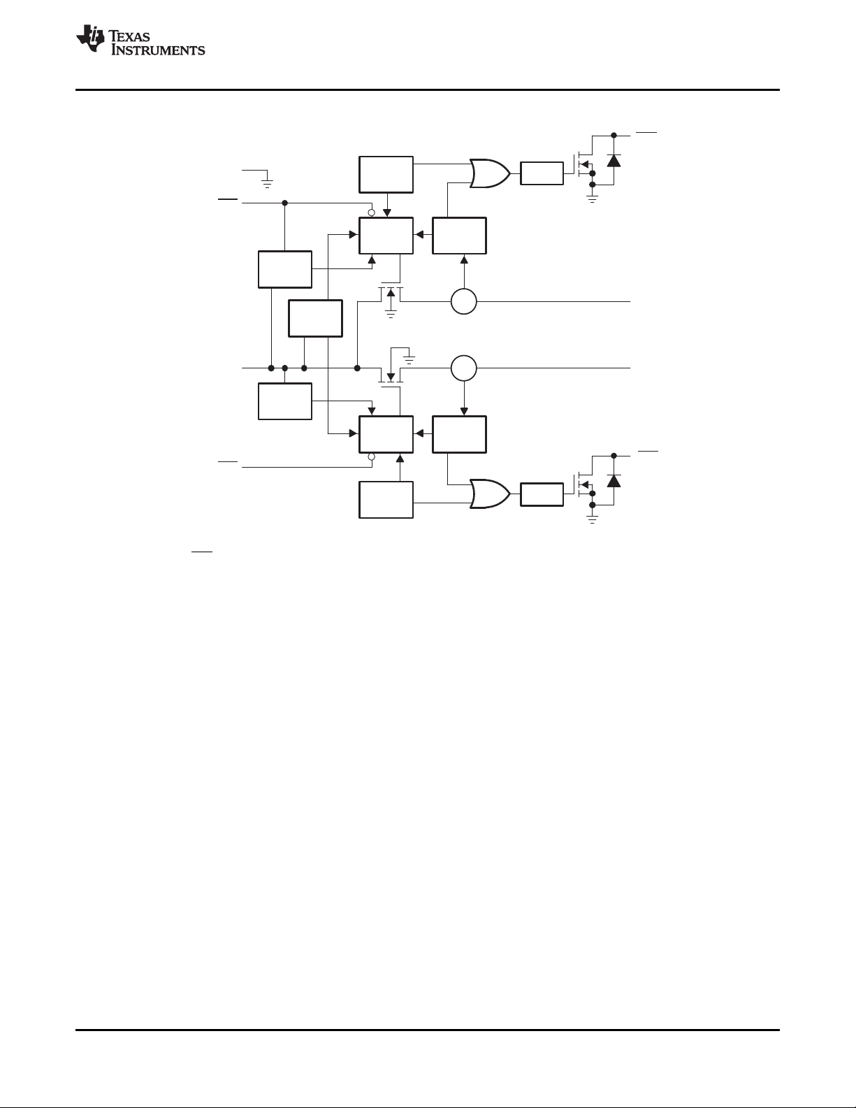
Thermal
Sense
Driver
Current
Limit
Charge
Pump
UVLO
CS
Driver
Current
Limit
CS
Thermal
Sense
Charge
Pump
GND
EN1
IN
EN2
OC1
OUT1
OUT2
OC2
Deglitch
Deglitch
(SeeNote A)
(SeeNote A)
(SeeNoteB)
(SeeNoteB)
TPS2060, TPS2064
TPS2068, TPS2069
www.ti.com
SLVS553K –MARCH 2005– REVISED MAY 2011
Functional Block Diagram (TPS2060 and TPS2064)
A. Current sense.
B. Active low (ENx) for TPS2060. Active high (ENx) for TPS2064.
Copyright © 2005–2011, Texas Instruments Incorporated 5
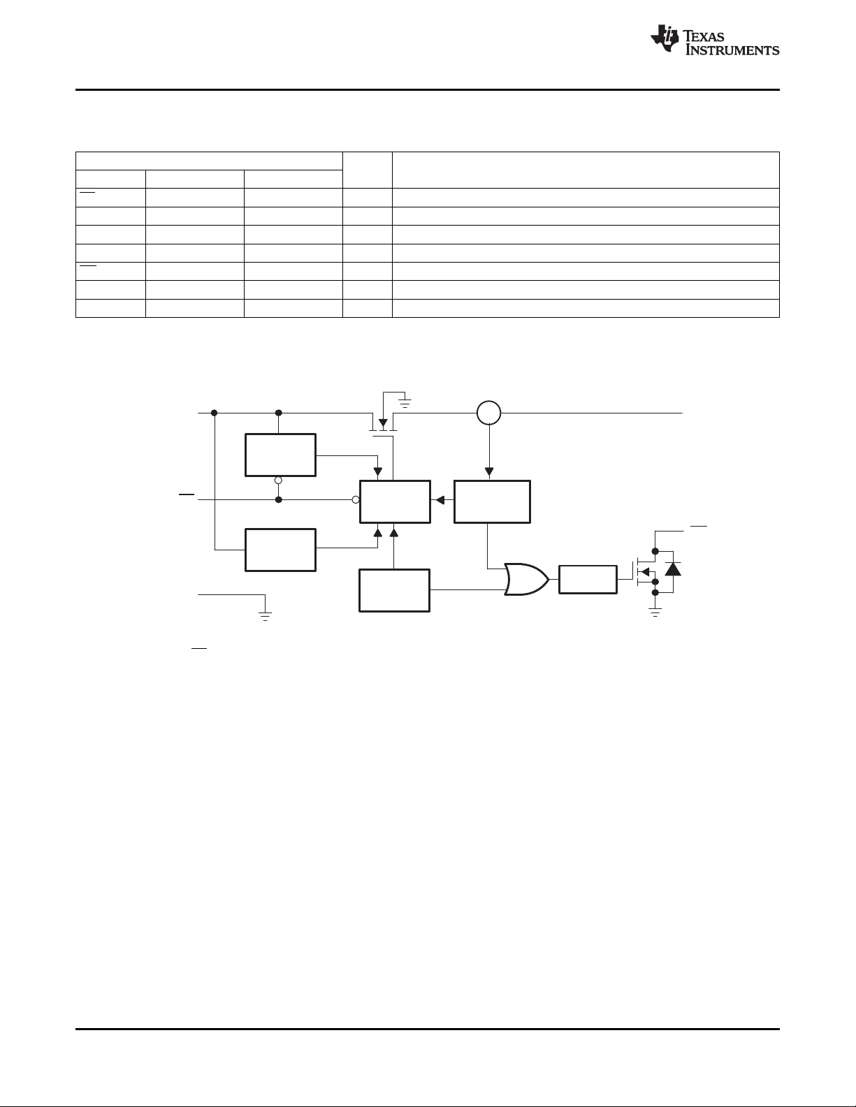
OUT
OC
IN
EN
GND
Current
Limit
Driver
UVLO
Charge
Pump
CS
Thermal
Sense
Deglitch
(SeeNote A)
(SeeNoteB)
TPS2060, TPS2064
TPS2068, TPS2069
SLVS553K –MARCH 2005– REVISED MAY 2011
www.ti.com
DEVICE INFORMATION
Pin Functions (TPS2068 and TPS2069)
PINS
I/O DESCRIPTION
NAME TPS2068 TPS2069
EN 4 — I Enable input, logic low turns on power switch
EN — 4 I Enable input, logic high turns on power switch
GND 1 1 Ground
IN 2, 3 2, 3 I Input voltage
OC 5 5 O Overcurrent, open-drain output, active-low
OUT 6, 7, 8 6, 7, 8 O Power-switch output
PowerPad PowerPad Connect to GND (DGN Package Only)
(1)
(1) See the Recommended Operating Conditions Table for PowerPad connection guidelines to meet qualifying conditions for CB Certificate
(DGN package only).
Functional Block Diagram (TPS2068 and TPS2069)
A. Current sense.
B. Active low (EN) for TPS2068. Active high (EN) for TPS2069.
6 Copyright © 2005–2011, Texas Instruments Incorporated
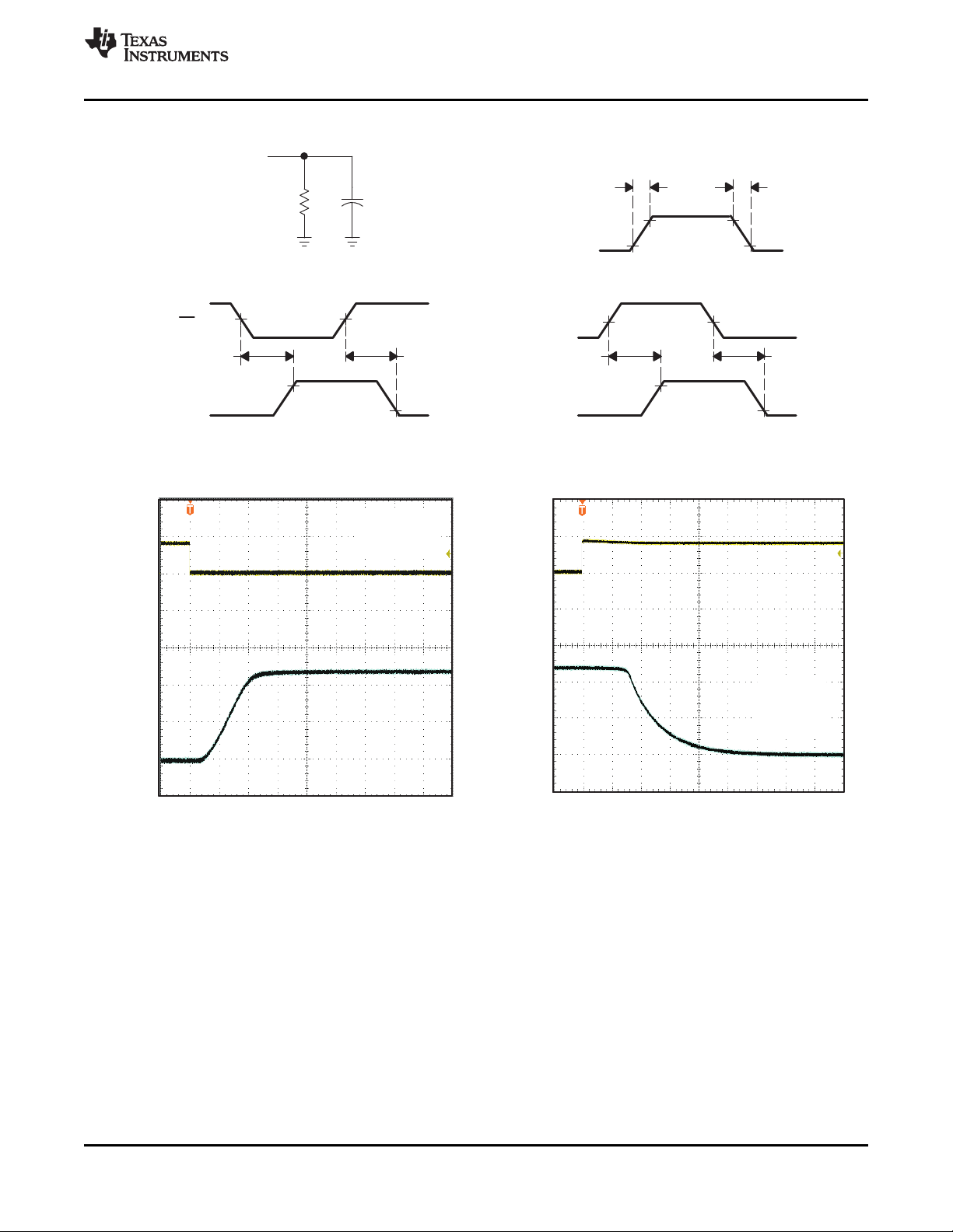
R
L
C
L
OUT
t
r
t
f
90%
90%
10%
10%
50%
50%
90%
10%
V
O(OUT)
V
I(EN)
V
O(OUT)
VOLTAGE WAVEFORMS
TEST CIRCUIT
t
on
t
off
50%
50%
90%
10%
V
I(EN)
V
O(OUT)
t
on
t
off
V
I(EN)
5V/div
V
O(OUT)
2V/div
t-Time-400 sm
R =5
C =1 F,
L
L
W
m
,
=25 CT
A
°
V
I(EN)
5V/div
V
O(OUT)
2V/div
t-Time-400 sm
R =5
C =1 F,
L
L
W
m
,
=25 CT
A
°
TPS2060, TPS2064
TPS2068, TPS2069
www.ti.com
SLVS553K –MARCH 2005– REVISED MAY 2011
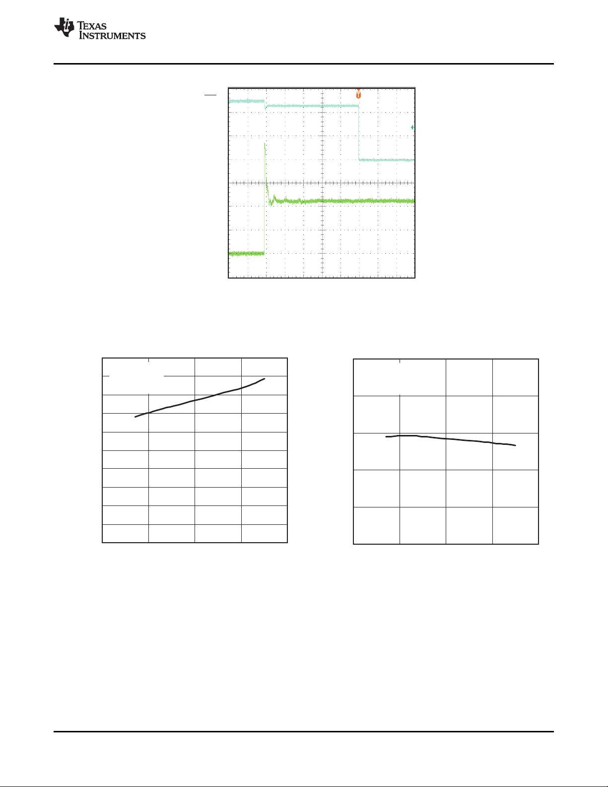
PARAMETER MEASUREMENT INFORMATION
Figure 1. Test Circuit and Voltage Waveforms
Figure 2. Turnon Delay and Rise Time With 1-μF Figure 3. Turnoff Delay and Fall Time With 1-μF
Load Load
Copyright © 2005–2011, Texas Instruments Incorporated 7
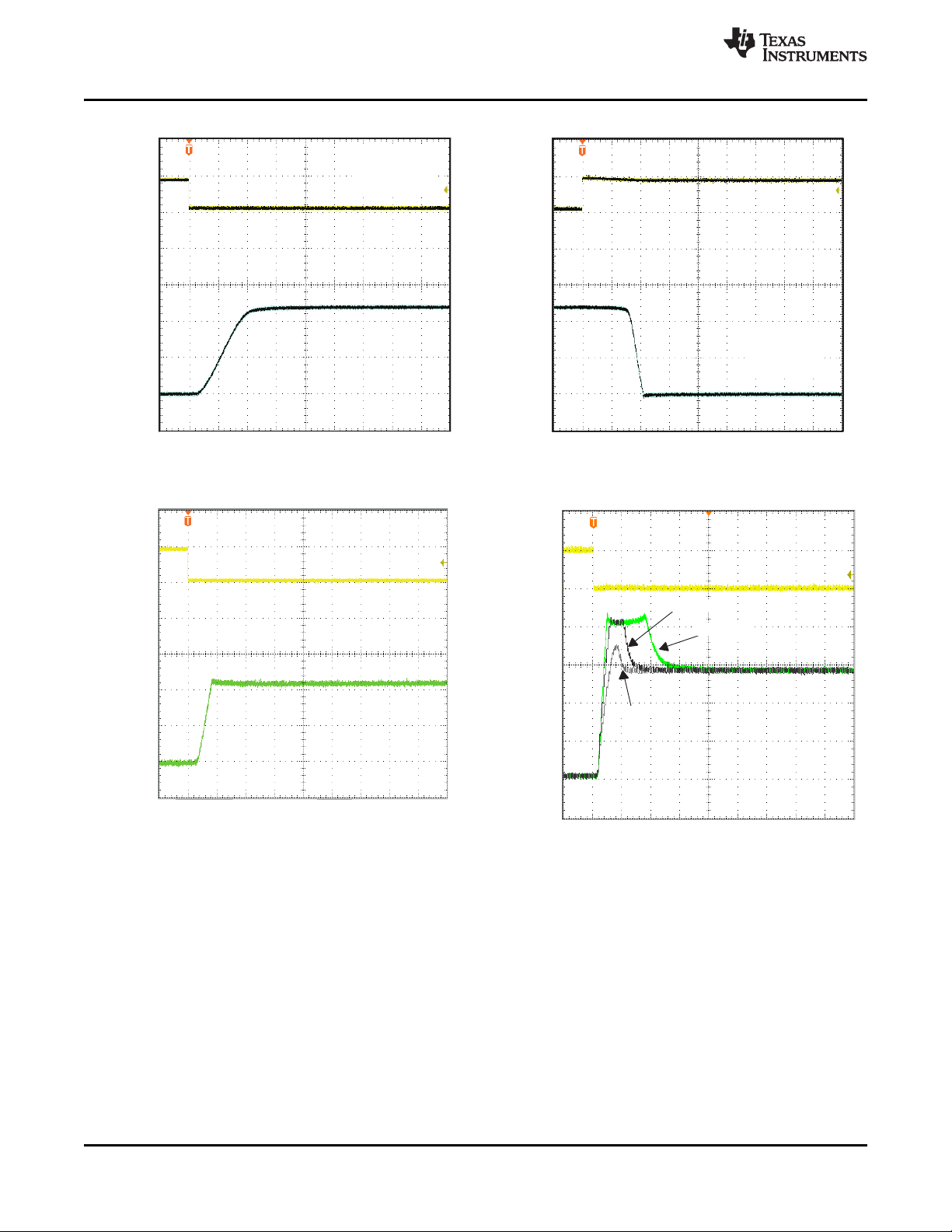
V
I(EN)
5V/div
V
O(OUT)
2V/div
t-Time-400 sm
R =5
C =100 F,
L
L
W
m
,
=25 CT
A
°
V
I(EN)
5V/div
V
O(OUT)
2V/div
t-Time-400 sm
R =5
C =100 F,
L
L
W
m
,
=25 CT
A
°
V
I(EN)
5 V/div
I
O(OUT)
1 A/div
t − Time − 500 ms/div
220 mF
470 mF
100 mF
V
I(EN)
5 V/div
I
O(OUT)
500 mA/div
t − Time − 500 ms/div
V
IN
= 5 V ,
R
L
= 3 W,
T
A
= 255C
TPS2060, TPS2064
TPS2068, TPS2069
SLVS553K –MARCH 2005– REVISED MAY 2011
www.ti.com
PARAMETER MEASUREMENT INFORMATION (continued)
Figure 4. Turnon Delay and Rise Time With 100-μF Figure 5. Turnoff Delay and Fall Time With 100-μF
Load Load
Figure 6. Short-Circuit Current, Figure 7. Inrush Current With Different
Device Enabled Into Short Load Capacitance
8 Copyright © 2005–2011, Texas Instruments Incorporated
V
O( )OCx
2V/div
I
O(OUT)
1 A/div
t-Time-2ms/div
0
0.1
0.2
0.3
0.4
0.5
0.6
0.7
0.8
0.9
1.0
2 3 4 5 6
Turnon Time − ms
V
I
− Input Voltage − V
C
L
= 100 mF,
R
L
= 5 W,
T
A
= 255C
1.5
1.6
1.7
1.8
1.9
2
2 3 4 5 6
C
L
= 100 mF,
R
L
= 5 W,
T
A
= 255C
Turnoff Time − mS
V
I
− Input Voltage − V
TPS2060, TPS2064
TPS2068, TPS2069
www.ti.com
SLVS553K –MARCH 2005– REVISED MAY 2011
PARAMETER MEASUREMENT INFORMATION (continued)
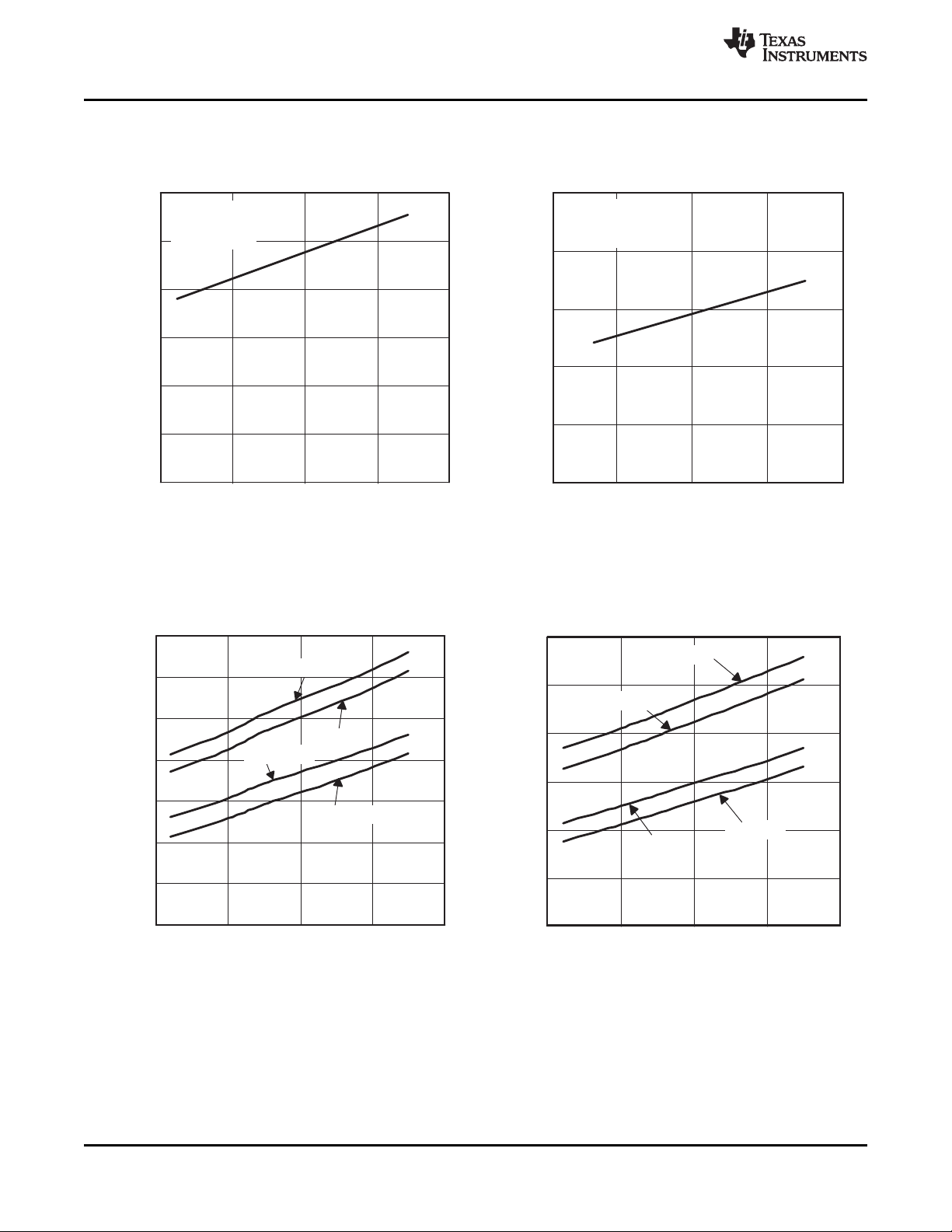
Figure 8. 0.6-Ω Load Connected to Enabled Device
TYPICAL CHARACTERISTICS
TURNON TIME TURNOFF TIME
vs vs
INPUT VOLTAGE INPUT VOLTAGE
Figure 9. Figure 10.
Copyright © 2005–2011, Texas Instruments Incorporated 9
0
0.1
0.2
0.3
0.4
0.5
0.6
2 3 4 5 6
Rise Time − ms
V
I
− Input Voltage − V
C
L
= 1 mF,
R
L
= 5 W,
T
A
= 255C
0
0.05
0.1
0.15
0.2
0.25
2 3 4 5 6
C
L
= 1 mF,
R
L
= 5 W,
T
A
= 255C
Fall Time − ms
V
I
− Input Voltage − V
0
10
20
30
40
50
60
70
−50 0 50 100 150
V
I
= 5.5 V
V
I
= 5 V
V
I
= 3.3 V
V
I
= 2.7 V
T
J
− Junction Temperature − 5C
− Supply Current, Output Enabled −
I
I (IN)
Aµ
0
10
20
40
50
60
-50
0 50 100 150
30
T -JunctionTemperature- C
J
°
I -SupplyCurrent,OutputEnabled- A
I(IN)
m
V =5.5V
I
V =3.3V
I
V =2.7V
I
V =5V
I
TPS2060, TPS2064
TPS2068, TPS2069
SLVS553K –MARCH 2005– REVISED MAY 2011
www.ti.com
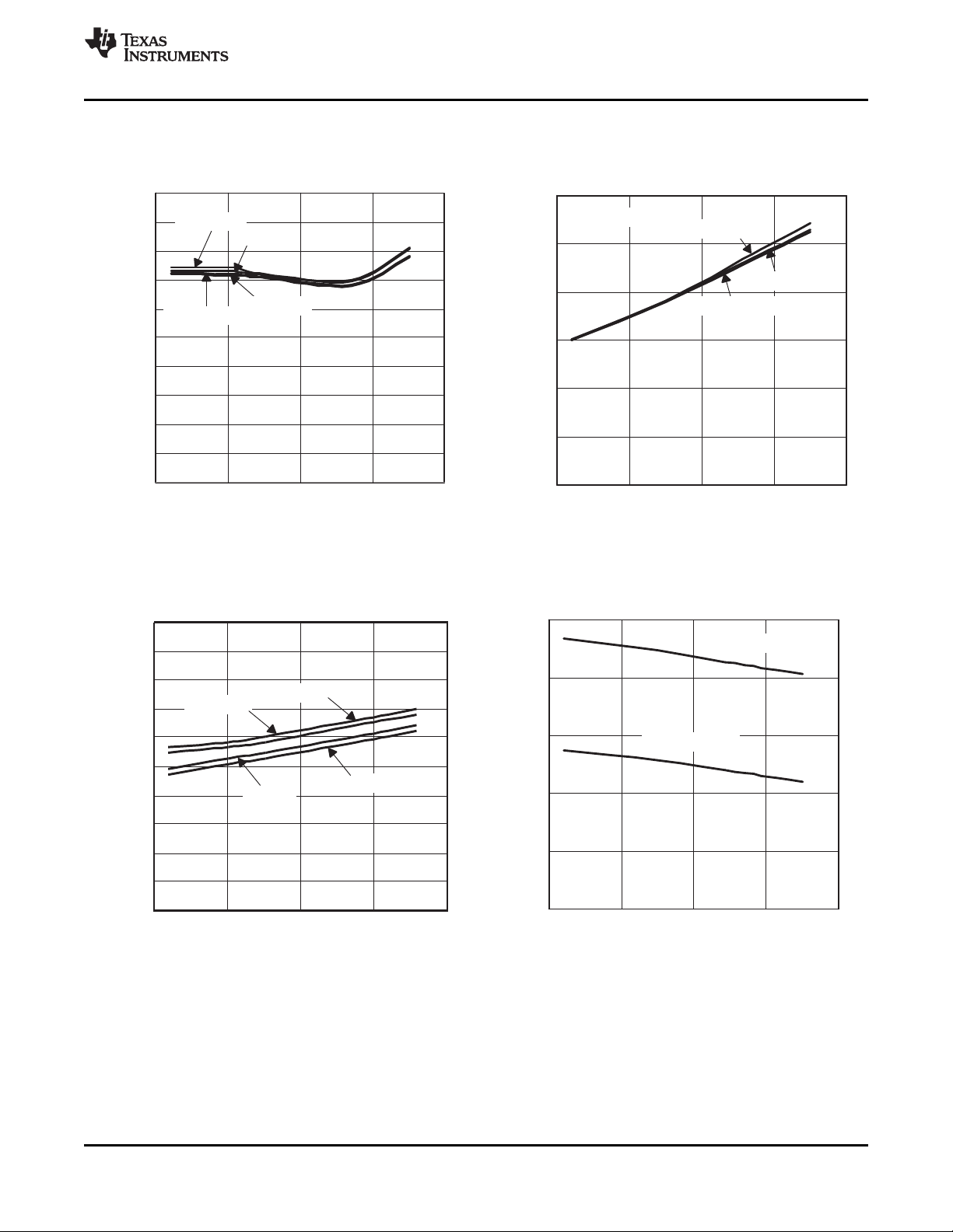
TYPICAL CHARACTERISTICS (continued)
RISE TIME FALL TIME
vs vs
INPUT VOLTAGE INPUT VOLTAGE
Figure 11. Figure 12.
TPS2060, TPS2064 TPS2068, TPS2069
SUPPLY CURRENT, OUTPUT ENABLED SUPPLY CURRENT, OUTPUT ENABLED
vs vs
JUNCTION TEMPERATURE JUNCTION TEMPERATURE
Figure 13. Figure 14.
10 Copyright © 2005–2011, Texas Instruments Incorporated
0
0.05
0.1
0.15
0.2
0.25
0.3
0.35
0.4
0.45
0.5
−50 0 50 100 150
V
I
= 5.5 V
V
I
= 5 V
V
I
= 3.3 V
V
I
= 2.7 V
T
J
− Junction Temperature − 5C
− Supply Current, Output Disabled −
I
I (IN)
Aµ
0
20
40
60
80
100
120
−50 0 50 100 150
Out1 = 5 V
Out1 = 3.3 V
Out1 = 2.7 V
I
O
= 0.5 A
T
J
− Junction Temperature − 5C
r
DS(on) − Static Drain-Source
On-State Resistance − mΩ
2.1
2.14
2.18
2.22
2.26
2.3
−50 0 50 100 150
UVLO Rising
UVLO Falling
UVOL − Undervoltage Lockout − V
T
J
− Junction Temperature − 5C
1.6
1.7
1.8
1.9
2
2.2
2.3
2.4
2.5
2.6
-50
0 50 100 150
2.1
T -JunctionTemperature- C
J
°
I -Short-CircuitCurrentLimit- A
OS
V =2.7V
I
V =3.3V
I
V =5V
I
V =5.5V
I
TPS2060, TPS2064
TPS2068, TPS2069
www.ti.com
SLVS553K –MARCH 2005– REVISED MAY 2011
TYPICAL CHARACTERISTICS (continued)
SUPPLY CURRENT, OUTPUT DISABLED STATIC DRAIN-SOURCE ON-STATE RESISTANCE
vs vs
JUNCTION TEMPERATURE JUNCTION TEMPERATURE
Figure 15. Figure 16.
SHORT-CIRCUIT OUTPUT CURRENT UNDERVOLTAGE LOCKOUT
vs vs
JUNCTION TEMPERATURE JUNCTION TEMPERATURE
Figure 17. Figure 18.
Copyright © 2005–2011, Texas Instruments Incorporated 11
Loading...