


TMS320F240PQS
Table of contents
 Loading...
D
High-Performance Static CMOS Technology
D
Includes the T320C2xLP Core CPU
– Object Compatible With the TMS320C2xx
– Source Code Compatible With
TMS320C25
– Upwardly Compatible With TMS320C5x
– 132-Pin Plastic Quad Flat Package
(PQ Suffix)
– 50-ns Instruction Cycle Time
D
Industrial and Automotive Temperature
Available
D
Memory
– 544 Words × 16 Bits of On-Chip
Data/Program Dual-Access RAM
– 16K Words × 16 Bits of On-Chip Program
ROM (’C240)/Flash EEPROM (’F240)
– 224K Words × 16 Bits of Total Memory
Address Reach (64K Data, 64K Program
and 64K I/O, and 32K Global Memory
Space)
D
Event-Manager Module
– 12 Compare/Pulse-Width Modulation
(PWM) Channels
– Three 16-Bit General-Purpose Timers
With Six Modes, Including Continuous
Upand Up/Down Counting
– Three 16-Bit Full-Compare Units With
Deadband
– Three 16-Bit Simple-Compare Units
– Four Capture Units (Two With
Quadrature Encoder-Pulse Interface
Capability)
TMS320C240, TMS320F240
DSP CONTROLLERS
SPRS042D – OCTOBER 1996 – REVISED NOVEMBER 1998
D
Dual 10-Bit Analog-to-Digital Conversion
Module
D
28 Individually Programmable, Multiplexed
I/O Pins
D
Phase-Locked-Loop (PLL)-Based Clock
Module
D
Watchdog Timer Module (With Real-Time
Interrupt)
D
Serial Communications Interface (SCI)
Module
D
Serial Peripheral Interface (SPI) Module
D
Six External Interrupts (Power Drive
Protect, Reset, NMI, and Three Maskable
Interrupts)
D
Four Power-Down Modes for Low-Power
Operation
D
Scan-Based Emulation
D
Development Tools Available:
– Texas Instruments (TI) ANSI
C Compiler, Assembler/Linker, and
C-Source Debugger
– Scan-Based Self-Emulation (XDS510)
– Third-Party Digital Motor Control and
Fuzzy-Logic Development Support
description
The TMS320C240 and TMS320F240 devices are the first members of a new family of DSP controllers based
on the TMS320C2xx generation of 16-bit fixed-point digital signal processors (DSPs). Unless otherwise noted,
the term ’x240 refers to both the TMS320C240 and the TMS320F240. Table 1 provides a comparison of the
features of each device. The only difference between these two devices is the type of program memory: the
’C240 contains 16K words of ROM and the ’F240 contains 16K words of flash. This new family is optimized for
digital motor/motion control applications. The DSP controllers combine the enhanced TMS320 architectural
design of the ’C2xLP core CPU for low-cost, high-performance processing capabilities and several advanced
peripherals optimized for motor/motion control applications. These peripherals include the event manager
module, which provides general-purpose timers and compare registers to generate up to 12 PWM outputs, and
a dual10-bit analog-to-digital converter (ADC), which can perform two simultaneous conversions within 6.1 µs.
See the functional block diagram.
Please be aware that an important notice concerning availability, standard warranty, and use in critical applications of
Texas Instruments semiconductor products and disclaimers thereto appears at the end of this data sheet.
TI and XDS510 are trademarks of Texas Instruments Incorporated.
PRODUCTION DATA information is current as of publication date.
Products conform to specifications per the terms of Texas Instruments
standard warranty. Production processing does not necessarily include
testing of all parameters.
POST OFFICE BOX 1443 • HOUSTON, TEXAS 77251–1443
Copyright 1998, Texas Instruments Incorporated
1

TMS320C240, TMS320F240
DSP CONTROLLERS
SPRS042D – OCTOBER 1996 – REVISED NOVEMBER 1998
description 1. . . . . . . . . . . . . . . . . . . . . . . . . . . . . . . . . . . . . . . . . . . . . . . . . . . . . . . .
PQ Package (Top View) 5. . . . . . . . . . . . . . . . . . . . . . . . . . . . . . . . . . . . . . . . . . . . .
terminal functions 6. . . . . . . . . . . . . . . . . . . . . . . . . . . . . . . . . . . . . . . . . . . . . . . . . .
functional block diagram 12. . . . . . . . . . . . . . . . . . . . . . . . . . . . . . . . . . . . . . . . . . .
architectural overview 13. . . . . . . . . . . . . . . . . . . . . . . . . . . . . . . . . . . . . . . . . . . . . .
system-level functions 13. . . . . . . . . . . . . . . . . . . . . . . . . . . . . . . . . . . . . . . . . . . . .
device memory map 13. . . . . . . . . . . . . . . . . . . . . . . . . . . . . . . . . . . . . . . . . . . . . . .
peripheral memory map 15. . . . . . . . . . . . . . . . . . . . . . . . . . . . . . . . . . . . . . . . . . .
digital I/O and shared pin functions 16. . . . . . . . . . . . . . . . . . . . . . . . . . . . . . . . . .
description of group1 shared I/O pins 16. . . . . . . . . . . . . . . . . . . . . . . . . . . . .
description of group2 shared I/O pins 18. . . . . . . . . . . . . . . . . . . . . . . . . . . . .
digital I/O control registers 18. . . . . . . . . . . . . . . . . . . . . . . . . . . . . . . . . . . . . . . . .
device reset and interrupts 18. . . . . . . . . . . . . . . . . . . . . . . . . . . . . . . . . . . . . . . . .
reset 19. . . . . . . . . . . . . . . . . . . . . . . . . . . . . . . . . . . . . . . . . . . . . . . . . . . . . . . . . .
hardware-generated interrupts 20. . . . . . . . . . . . . . . . . . . . . . . . . . . . . . . . . . .
external interrupts 26. . . . . . . . . . . . . . . . . . . . . . . . . . . . . . . . . . . . . . . . . . . . . .
clock generation 27. . . . . . . . . . . . . . . . . . . . . . . . . . . . . . . . . . . . . . . . . . . . . . . . . .
low-power modes 29. . . . . . . . . . . . . . . . . . . . . . . . . . . . . . . . . . . . . . . . . . . . . . . . .
functional block diagram of the TMS320x240 DSP CPU 30. . . . . . . . . . . . . . .
’x240 DSP core CPU 33. . . . . . . . . . . . . . . . . . . . . . . . . . . . . . . . . . . . . . . . . . . . . . . .
status and control registers 33. . . . . . . . . . . . . . . . . . . . . . . . . . . . . . . . . . . . . . . .
central processing unit 34. . . . . . . . . . . . . . . . . . . . . . . . . . . . . . . . . . . . . . . . . . . . .
input scaling shifter 34. . . . . . . . . . . . . . . . . . . . . . . . . . . . . . . . . . . . . . . . . . . . .
multiplier 34. . . . . . . . . . . . . . . . . . . . . . . . . . . . . . . . . . . . . . . . . . . . . . . . . . . . . .
central arithmetic logic unit 36. . . . . . . . . . . . . . . . . . . . . . . . . . . . . . . . . . . . . .
accumulator 37. . . . . . . . . . . . . . . . . . . . . . . . . . . . . . . . . . . . . . . . . . . . . . . . . . .
auxiliary registers and auxiliary-register arithmetic unit (ARAU) 37. . . . . . . . .
internal memory 37. . . . . . . . . . . . . . . . . . . . . . . . . . . . . . . . . . . . . . . . . . . . . . . . . . .
dual-access RAM (DARAM) 37. . . . . . . . . . . . . . . . . . . . . . . . . . . . . . . . . . . . . . . .
ROM (TMS320C240 only) 38. . . . . . . . . . . . . . . . . . . . . . . . . . . . . . . . . . . . . . . . .
flash EEPROM (TMS320F240 only) 38. . . . . . . . . . . . . . . . . . . . . . . . . . . . . . . . .
flash serial loader 38. . . . . . . . . . . . . . . . . . . . . . . . . . . . . . . . . . . . . . . . . . . . . .
flash control mode register 38. . . . . . . . . . . . . . . . . . . . . . . . . . . . . . . . . . . . . . .
peripherals 39. . . . . . . . . . . . . . . . . . . . . . . . . . . . . . . . . . . . . . . . . . . . . . . . . . . . . . . .
external memory interface 39. . . . . . . . . . . . . . . . . . . . . . . . . . . . . . . . . . . . . . . . .
Contents
INTRODUCTION
DETAILED DESCRIPTION
2
POST OFFICE BOX 1443 • HOUSTON, TEXAS 77251–1443

TMS320C240, TMS320F240
DSP CONTROLLERS
SPRS042D – OCTOBER 1996 – REVISED NOVEMBER 1998
Contents
DETAILED DESCRIPTION (continued)
event-manager (EV) module 40. . . . . . . . . . . . . . . . . . . . . . . . . . . . . . . . . . . . .
general-purpose (GP) timers 40. . . . . . . . . . . . . . . . . . . . . . . . . . . . . . . . . .
full compare units 42. . . . . . . . . . . . . . . . . . . . . . . . . . . . . . . . . . . . . . . . . . .
programmable-deadband generator 42. . . . . . . . . . . . . . . . . . . . . . . . . . . .
simple compares 42. . . . . . . . . . . . . . . . . . . . . . . . . . . . . . . . . . . . . . . . . . . . .
compare/PWM waveform generation 42. . . . . . . . . . . . . . . . . . . . . . . . . . . .
compare/PWMs characteristics 42
capture unit 42. . . . . . . . . . . . . . . . . . . . . . . . . . . . . . . . . . . . . . . . . . . . . . . . . .
quadrature-encoder pulse (QEP) circuit 43. . . . . . . . . . . . . . . . . . . . . . . . .
analog-to-digital converter (ADC) module 43. . . . . . . . . . . . . . . . . . . . . . . . . .
serial peripheral interface (SPI) module 45. . . . . . . . . . . . . . . . . . . . . . . . . . . .
serial communications interface (SCI) module 47. . . . . . . . . . . . . . . . . . . . . .
watchdog (WD) and real-time interrupt (RTI) module 49. . . . . . . . . . . . . . . .
scan-based emulation 51. . . . . . . . . . . . . . . . . . . . . . . . . . . . . . . . . . . . . . . . . . . .
TMS320x240 instruction set 51. . . . . . . . . . . . . . . . . . . . . . . . . . . . . . . . . . . . . . .
addressing modes 51. . . . . . . . . . . . . . . . . . . . . . . . . . . . . . . . . . . . . . . . . . . . . .
repeat feature 51. . . . . . . . . . . . . . . . . . . . . . . . . . . . . . . . . . . . . . . . . . . . . . . . . .
instruction set summary 52. . . . . . . . . . . . . . . . . . . . . . . . . . . . . . . . . . . . . . . . .
development support 58. . . . . . . . . . . . . . . . . . . . . . . . . . . . . . . . . . . . . . . . . . . . .
device and development-support tool nomenclature 59. . . . . . . . . . . . . . . .
documentation support 60. . . . . . . . . . . . . . . . . . . . . . . . . . . . . . . . . . . . . . . . . . .
. . . . . . . . . . . . . . . . . . . . . . . . . . . . . . . . .
ELECTRICAL SPECIFICATIONS
absolute maximum ratings over operating free-air temperature range 61.
recommended operating conditions 61. . . . . . . . . . . . . . . . . . . . . . . . . . . . . . . . .
output current variation with output voltage: SPICE simulation results 62
elec characteristics over recommended oper free-air temperature range 62
signal transition levels 63. . . . . . . . . . . . . . . . . . . . . . . . . . . . . . . . . . . . . . . . . . . . .
timing parameter symbology 65. . . . . . . . . . . . . . . . . . . . . . . . . . . . . . . . . . . . . . . .
general notes on timing parameters 65. . . . . . . . . . . . . . . . . . . . . . . . . . . . . . . . .
clock options 66. . . . . . . . . . . . . . . . . . . . . . . . . . . . . . . . . . . . . . . . . . . . . . . . . . . . . .
timings with the PLL circuit disabled 66. . . . . . . . . . . . . . . . . . . . . . . . . . . . . . . . .
external reference crystal with PLL-circuit-enabled clock option 67. . . . . . . . .
timings with the PLL circuit enabled 67. . . . . . . . . . . . . . . . . . . . . . . . . . . . . . . . .
low-power mode timings 69. . . . . . . . . . . . . . . . . . . . . . . . . . . . . . . . . . . . . . . . . . .
POST OFFICE BOX 1443 • HOUSTON, TEXAS 77251–1443
3

TMS320C240, TMS320F240
DSP CONTROLLERS
SPRS042D – OCTOBER 1996 – REVISED NOVEMBER 1998
ELECTRICAL SPECIFICATIONS (continued)
Contents
memory and parallel I/O interface
memory and parallel I/O interface
I/O timing variation with load capacitance: SPICE simulation results 75. . .
READY timings 76. . . . . . . . . . . . . . . . . . . . . . . . . . . . . . . . . . . . . . . . . . . . . . . . . . . .
RS and PORESET timings 77. . . . . . . . . . . . . . . . . . . . . . . . . . . . . . . . . . . . . . . . . .
XF, BIO, and MP/MC timings 79. . . . . . . . . . . . . . . . . . . . . . . . . . . . . . . . . . . . . . . .
PWM/CMP timings 80. . . . . . . . . . . . . . . . . . . . . . . . . . . . . . . . . . . . . . . . . . . . . . . . .
capture and QEP timings 81. . . . . . . . . . . . . . . . . . . . . . . . . . . . . . . . . . . . . . . . . . .
interrupt timings 82. . . . . . . . . . . . . . . . . . . . . . . . . . . . . . . . . . . . . . . . . . . . . . . . . . .
general-purpose input/output timings 83. . . . . . . . . . . . . . . . . . . . . . . . . . . . . . .
serial communications interface (SCI) I/O timings 84. . . . . . . . . . . . . . . . . . . .
SPI master mode external timing parameters (clock phase = 0) 85. . . . . . . .
SPI master mode external timing parameters (clock phase = 1) 87. . . . . . . .
SPI slave mode external timing parameters (clock phase = 0) 89. . . . . . . . .
SPI slave mode external timing parameters (clock phase = 1) 91. . . . . . . . .
10-bit dual analog-to-digital converter (ADC) 93. . . . . . . . . . . . . . . . . . . . . . . . .
ADC input pin circuit 94. . . . . . . . . . . . . . . . . . . . . . . . . . . . . . . . . . . . . . . . . . . . . . .
flash EEPROM 96. . . . . . . . . . . . . . . . . . . . . . . . . . . . . . . . . . . . . . . . . . . . . . . . . . . . .
programming operation 96. . . . . . . . . . . . . . . . . . . . . . . . . . . . . . . . . . . . . . . . . . . .
erase operation 96. . . . . . . . . . . . . . . . . . . . . . . . . . . . . . . . . . . . . . . . . . . . . . . . . . .
flash-write operation 96. . . . . . . . . . . . . . . . . . . . . . . . . . . . . . . . . . . . . . . . . . . . . . .
register file compilation 97. . . . . . . . . . . . . . . . . . . . . . . . . . . . . . . . . . . . . . . . . . . .
package drawing, PQ (S-PQFP-G***), PLASTIC QUAD FLATPACK 104. . . . . .
read
timings 71. . . . . . . . . . . . . . . . . . . . . . .
write
timings 73. . . . . . . . . . . . . . . . . . . . . .
4
POST OFFICE BOX 1443 • HOUSTON, TEXAS 77251–1443
TMS320C240, TMS320F240
DSP CONTROLLERS
SPRS042D – OCTOBER 1996 – REVISED NOVEMBER 1998
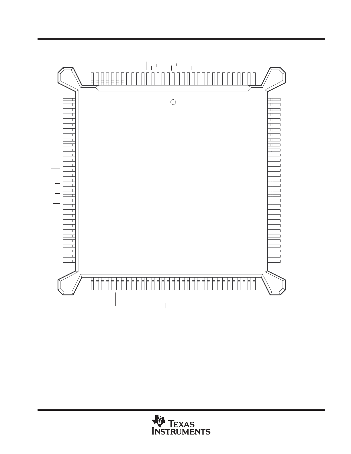
PQ PACKAGE
(TOP VIEW)
V
DV
DD
D10
D11
D12
D13
D14
D15
V
TCK
TDI
TRST
TMS
TDO
RS
READY
MP/MC
EMU0
EMU1/OFF
NMI
PORESET
RESERVED
SCIRXD/IO
SCITXD/IO
SPISIMO/IO
V
DV
DD
SPISOMI/IO
SPICLK/IO
WDDIS
D7
D8
SS
D9
SS
SS
DD
SS
V
D5
D4
D3D6D2
DV
12
13
14
15
16
17
18
19
20
21
22
23
24
25
26
27
28
29
30
31
32
33
34
35
36
37
38
39
40
41
42
43
44
45
46
47
48
†
49
50
525354
555156
SS
DD
D0
CV
D1
11
10
STRBBRR/W
CV
9
867
TMS320C240
TMS320F240
58
59
6067626361
DD
SS
V
DV
234
5
64
65
66
ISDSA15
A14
A13
128
127
126
A12
125
W/R
PS
WE
1
131
129
130
132
695768
70717273747576777879808182
A11
124
A10
123
A9
122
DV
121
DD
SS
V
120
A8A7A6
119
118
117
116
115
114
113
112
111
110
109
108
107
106
105
104
103
102
101
100
99
98
97
96
95
94
93
92
91
90
89
88
87
86
85
84
83
A5
A4
A3
V
SS
A2
A1
A0
TMRCLK/IOPB7
TMRDIR/IOPB6
T3PWM/T3CMP/IOPB5
T2PWM/T2CMP/IOPB4
T1PWM/T1CMP/IOPB3
V
SS
DV
DD
PWM9/CMP9/IOPB2
PWM8/CMP8/IOPB1
PWM7/CMP7/IOPB0
PWM6/CMP6
PWM5/CMP5
PWM4/CMP4
PWM3/CMP3
PWM2/CMP2
PWM1/CMP1
DV
DD
V
SS
ADCIN8/IOPA3
ADCIN9/IOPA2
ADCIN10
ADCIN11
V
SSA
V
REFLO
V
REFHI
V
CCA
XINT1
PDPINT
XINT3/IO
XINT2/IO
SPISTE/IO
†
For the TMS320F240 devices, this pin is V
OSCBYP
DD
SS
DD
VSSV
CV
XTAL2
XTAL1/CLKIN
DV
XF/IOPC2
BIO/IOPC3
CLKOUT/IOPC1
ADCSOC/IOPC0
/WDDIS.
CCP
POST OFFICE BOX 1443 • HOUSTON, TEXAS 77251–1443
CAP1/QEP1/IOPC4
SS
V
CAP3/IOPC6
CAP4/IOPC7
ADCIN0/IOPA0
CAP2/QEP2/IOPC5
ADCIN1/IOPA1
ADCIN2
ADCIN3
ADCIN5
ADCIN4
ADCIN7
ADCIN6
ADCIN15
ADCIN14
ADCIN12
ADCIN13
5
TMS320C240, TMS320F240
TYPE
†
DESCRIPTION
DSP CONTROLLERS
SPRS042D – OCTOBER 1996 – REVISED NOVEMBER 1998
TERMINAL
NAME NO.
EXTERNAL INTERFACE DATA/ADDRESS SIGNALS
A0 (LSB)
A1
A2
A3
A4
A5
A6
A7
A8
A9
A10
A11
A12
A13
A14
A15 (MSB)
D0 (LSB)
D1
D2
D3
D4
D5
D6
D7
D8
D9
D10
D11
D12
D13
D14
D15 (MSB)
DS
PS
IS
READY 36 I
R/W 4 O/Z
STRB 6 O/Z
WE 1 O/Z
W/R 132 O/Z
†
I = input, O = output, Z = high impedance
110
111
112
114
115
116
117
118
119
122
123
124
125
126
127
128
9
10
11
12
15
16
17
18
19
22
23
24
25
26
27
28
129
131
130
O/Z
I/O/Z
O/Z
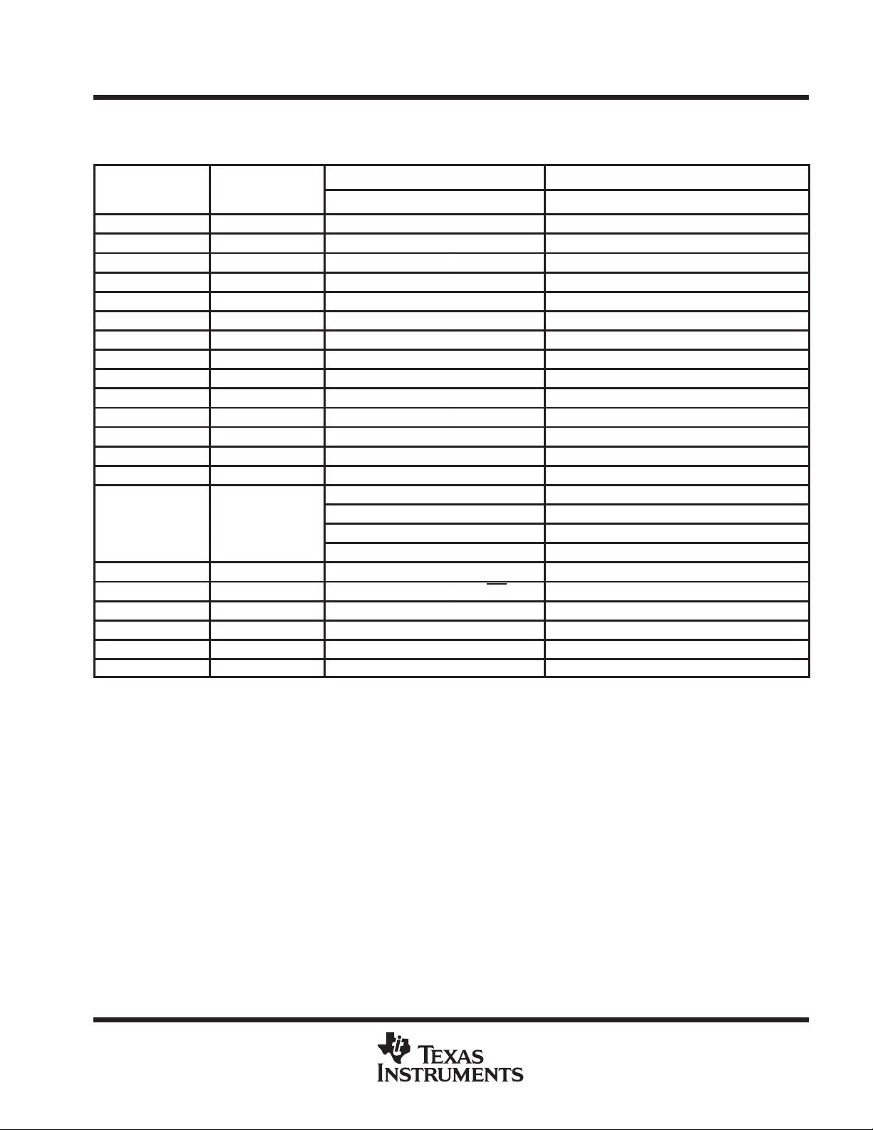
Parallel address bus A0 [least significant bit (LSB)] through A15 [most significant bit (MSB)]. A15–A0
are multiplexed to address external data/program memory or I/O. A15–A0 are placed in
high-impedance state when EMU1/OFF
modes.
Parallel data bus D0 (LSB) through D15 (MSB). D15–D0 are multiplexed to transfer data between the
TMS320x240 and external data/program memory and I/O space (devices). D15–D0 are placed in the
high-impedance state when not outputting, when in power-down mode, when reset (RS
or when EMU1/OFF
EXTERNAL INTERFACE CONTROL SIGNALS
Data, program, and I/O space select signals. DS, PS, and IS are always high unless low-level asserted
for communication to a particular external space. They are placed in the high-impedance state during
reset, power down, and when EMU1/OFF
Data ready. READY indicates that an external device is prepared for the bus transaction to be
completed. If the device is not ready (READY is low), the processor waits one cycle and checks
READY again.
Read/write signal. R/W indicates transfer direction during communication to an external device. It is
normally in read mode (high), unless low level is asserted for performing a write operation. It is placed
in the high-impedance state during reset, power down, and when EMU1/OFF
Strobe. STRB is always high unless asserted low to indicate an external bus cycle. It is placed in the
high-impedance state during reset, power down, and when EMU1/OFF
Write enable. The falling edge of WE indicates that the device is driving the external data bus
(D15–D0). Data can be latched by an external device on the rising edge of WE
external program, data, and I/O writes. WE
EMU1/OFF
Write/read. W/R is an inverted form of R/W and can connect directly to the output enable of external
devices. W/R
Terminal Functions
is active low and hold their previous states in power-down
) is asserted,
is active low.
is active low.
is active low.
is active low.
. WE is active on all
goes in the high-impedance state following reset and when
is active low.
is placed in the high-impedance state following reset and when EMU1/OFF is active low.
6
POST OFFICE BOX 1443 • HOUSTON, TEXAS 77251–1443
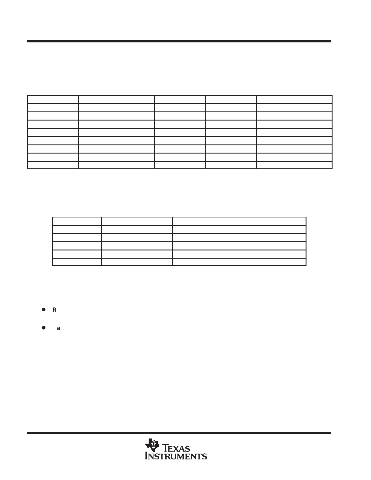
TYPE
†
DESCRIPTION
Analog inputs to the first ADC
Analog inputs to the second ADC
TERMINAL
NAME NO.
EXTERNAL INTERFACE CONTROL SIGNALS (CONTINUED)
BR 5 O/Z
‡
WDDIS
ADCIN2 74 I
ADCIN3 75 I
ADCIN4 76 I
ADCIN5 77 I
ADCIN6 78 I
ADCIN7 79 I
ADCIN10 89 I
ADCIN11 88 I
ADCIN12 83 I
ADCIN13 82 I
ADCIN14 81 I
ADCIN15 80 I
ADCIN0/IOPA0 72 I/O
ADCIN1/IOPA1 73 I/O
ADCIN9/IOPA2 90 I/O
ADCIN8/IOPA3 91 I/O
PWM7/CMP7/IOPB0 100 I/O/Z
PWM8/CMP8/IOPB1 101 I/O/Z
PWM9/CMP9/IOPB2 102 I/O/Z
†
I = input, O = output, Z = high impedance
‡
For the TMS320F240 devices, this pin is V
50 I
TMS320C240, TMS320F240
DSP CONTROLLERS
SPRS042D – OCTOBER 1996 – REVISED NOVEMBER 1998
Terminal Functions (Continued)
Bus request. BR is asserted during access of external global data memory space. BR can be
used to extend the data memory address space by up to 32K words. BR
high-impedance state during reset, power down, and when EMU1/OFF
Flash-programming voltage supply. If V
ENTIRE on-chip flash memory block—that is, for programming the flash. If V
WRITE/ERASE of the flash memory is not allowed, thereby protecting the entire memory block
from being overwritten. WDDIS also functions as a hardware watchdog disable. The watchdog
timer is disabled when V
ADC INPUTS (UNSHARED)
p
p
BIT I/O AND SHARED FUNCTIONS PINS
Bidirectional digital I/O.
Analog input to the first ADC.
ADCIN0/IOPA0 is configured as a digital input by all device resets.
Bidirectional digital I/O.
Analog input to the first ADC.
ADCIN1/IOPA1 is configured as a digital input by all device resets.
Bidirectional digital I/O.
Analog input to the second ADC.
ADCIN9/IOPA2 is configured as a digital input by all device resets.
Bidirectional digital I/O.
Analog input to the second ADC.
ADCIN8/IOPA3 is configured as a digital input by all device resets.
Bidirectional digital I/O. Simple compare/PWM 1 output. The state of PWM7/CMP7/IOPB0 is
determined by the simple compare/PWM and the simple action control register (SACTR). It
goes to the high-impedance state when unmasked PDPINT
PWM7/CMP7/IOPB0 is configured as a digital input by all device resets.
Bidirectional digital I/O. Simple compare/PWM 2 output. The state of PWM8/CMP8/IOPB1 is
determined by the simple compare/PWM and the SACTR. It goes to the high-impedance state
when unmasked PDPINT
by all device resets.
Bidirectional digital I/O. Simple compare/PWM 3 output. The state of PWM9/CMP9/IOPB2 is
determined by the simple compare/PWM and SACTR. It goes to the high-impedance state
when unmasked PDPINT
by all device resets.
CCP/WDDIS
.
/WDDIS = 5 V and bit 6 in WDCR is set to 1.
CCP
goes active low. PWM8/CMP8/IOPB1 is configured as a digital input
goes active low. PWM9/CMP9/IOPB2 is configured as a digital input
= 5 V, then WRITE/ERASE can be made to the
CCP
goes in the
is active low.
CCP
goes active low.
= 0 V , then
POST OFFICE BOX 1443 • HOUSTON, TEXAS 77251–1443
7
TMS320C240, TMS320F240
TYPE
†
DESCRIPTION
DSP CONTROLLERS
SPRS042D – OCTOBER 1996 – REVISED NOVEMBER 1998
Terminal Functions (Continued)
TERMINAL
NAME NO.
BIT I/O AND SHARED FUNCTIONS PINS (CONTINUED)
T1PWM/T1CMP/
IOPB3
T2PWM/T2CMP/
IOPB4
T3PWM/T3CMP/
IOPB5
TMRDIR/IOPB6 108 I/O
TMRCLK/IOPB7 109 I/O
ADCSOC/IOPC0 63 I/O
CAP1/QEP1/IOPC4 67 I/O
CAP2/QEP2/IOPC5 68 I/O
CAP3/IOPC6 69 I/O
CAP4/IOPC7 70 I/O
XF/IOPC2 65 I/O
BIO/IOPC3 66 I/O
CLKOUT/IOPC1 64 I/O
SCITXD/IO 44 I/O
SCIRXD/IO 43 I/O
†
I = input, O = output, Z = high impedance
105 I/O/Z
106 I/O/Z
107 I/O/Z
SERIAL COMMUNICATIONS INTERFACE (SCI) AND BIT I/O PINS
Bidirectional digital I/O. Timer 1 compare output. T1PWM/T1CMP/IOPB3 goes to the highimpedance state when unmasked PDPINT
input by all device resets.
Bidirectional digital I/O. Timer 2 compare output. T2PWM/T2CMP/IOPB4 goes to the highimpedance state when unmasked PDPINT
input by all device resets.
Bidirectional digital I/O. Timer 3 compare output. T3PWM/T3CMP/IOPB5 goes to the highimpedance state when unmasked PDPINT
input by all device resets.
Bidirectional digital I/O. Direction signal for the timers. Up-counting direction if TMRDIR/IOPB6
is low, down-counting direction if this pin is high.
This pin is configured as a digital input by all device resets.
Bidirectional digital I/O.
External clock input for general-purpose timers.
This pin is configured as a digital input by all device resets.
Bidirectional digital I/O.
External start of conversion input for ADC.
This pin is configured as a digital input by all device resets.
Bidirectional digital I/O.
Capture 1 or QEP 1 input.
This pin is configured as a digital input by all device resets.
Bidirectional digital I/O.
Capture 2 or QEP 2 input.
This pin is configured as a digital input by all device resets.
Bidirectional digital I/O.
Capture 3 input.
This pin is configured as a digital input by all device resets.
Bidirectional digital I/O.
Capture 4 input.
This pin is configured as a digital input by all device resets.
Bidirectional digital I/O. External flag output (latched software-programmable signal). XF is
used for signaling other processors in multiprocessing configurations or as a general-purpose
output pin. This pin is configured as an external flag output by all device resets.
Bidirectional digital I/O. Branch control input. BIO is polled by the BIOZ instruction. If BIO is low,
the CPU executes a branch. If BIO
as a branch-control input by all device resets.
Bidirectional digital I/O. Clock output. Clock output is selected by the CLKSRC bits in the
SYSCR register. This pin is configured as a DSP clock output by a power-on reset.
SCI asynchronous serial port transmit data, or general-purpose bidirectional I/O. This pin is
configured as a digital input by all device resets.
SCI asynchronous serial port receive data, or general-purpose bidirectional I/O. This pin is
configured as a digital input by all device resets.
goes active low. This pin is configured as a digital
goes active low. This pin is configured as a digital
goes active low. This pin is configured as a digital
is not used , it should be pulled high. This pin is configured
8
POST OFFICE BOX 1443 • HOUSTON, TEXAS 77251–1443
TYPE
†
DESCRIPTION
Terminal Functions (Continued)
TERMINAL
NAME NO.
SERIAL PERIPHERAL INTERFACE (SPI) AND BIT I/O PINS
SPISIMO/IO 45 I/O
SPISOMI/IO 48 I/O
SPICLK/IO 49 I/O
SPISTE/IO 51 I/O
PWM1/CMP1
PWM2/CMP2
PWM3/CMP3
PWM4/CMP4
PWM5/CMP5
PWM6/CMP6
RS 35 I/O
MP/MC 37 I
NMI 40 I
PORESET 41 I
XINT1 53 I External user interrupt no. 1
XINT2/IO 54 I/O
XINT3/IO 55 I/O
PDPINT 52 I
XTAL2 57 O
XTAL1/CLKIN 58 I/Z
OSCBYP 56 I Bypass oscillator if low
†
I = input, O = output, Z = high impedance
94
95
96
97
98
99
O/Z
SPI slave in, master out , or general-purpose bidirectional I/O. This pin is configured as a digital
input by all device resets.
SPI slave out, master in, or general-purpose bidirectional I/O. This pin is configured as a digital
input by all device resets.
SPI clock, or general-purpose bidirectional I/O. This pin is configured as a digital input by all
device resets.
SPI slave transmit enable (optional), or general-purpose bidirectional I/O. This pin is configured
as a digital input by all device resets.
COMPARE SIGNALS
Compare units compare or PWM outputs. The state of these pins is determined by the
compare/PWM and the full action control register (ACTR). CMP1–CMP6 go to the highimpedance state when unmasked PDPINT
INTERRUPT AND MISCELLANEOUS SIGNALS
Reset input. RS causes the TMS320x240 to terminate execution and sets PC = 0. When RS
is brought to a high level, execution begins at location zero of program memory. RS af fects (or
sets to zero) various registers and status bits.
MP/MC (microprocessor/microcomputer) select. If MP/MC is low, internal program memory is
selected. If it is high, external program memory is selected.
Nonmaskable interrupt. When NMI is activated, the device is interrupted regardless of the state
of the INTM bit of the status register. NMI has programmable polarity.
Power-on reset. PORESET causes the TMS320x240 to terminate execution and sets PC = 0.
When PORESET
memory. PORESET
tion, PORESET
External user interrupt no. 2. General-purpose bidirectional I/O. This pin is configured as a
digital input by all device resets.
External user interrupt no. 3. General-purpose bidirectional I/O. This pin is configured as a
digital input by all device resets.
Maskable power-drive protection interrupt. If PDPINT is unmasked and it goes active low, the
timer compare outputs immediately go to the high-impedance state.
PLL oscillator output. XT AL2 is tied to one side of a reference crystal when the device is in PLL
mode (CLKMD[1:0] = 1x, CKCR0.7–6). This pin can be left unconnected in oscillator bypass
mode (OSCBYP
low.
PLL oscillator input. XTAL1/CLKIN is tied to one side of a reference crystal in PLL mode
(CLKMD[1:0] = 1x, CKCR0.7–6), or is connected to an external clock source in oscillator
bypass mode (OSCBYP
is brought to a high level, execution begins at location zero of program
affects (or sets to zero) the same registers and status bits as RS. In addi-
initializes the PLL control registers.
CLOCK SIGNALS
≤ VIL). This pin goes in the high-impedance state when EMU1/OFF is active
TMS320C240, TMS320F240
DSP CONTROLLERS
SPRS042D – OCTOBER 1996 – REVISED NOVEMBER 1998
goes active low, and when reset (RS) is asserted.
≤ VIL).
POST OFFICE BOX 1443 • HOUSTON, TEXAS 77251–1443
9
TMS320C240, TMS320F240
TYPE
†
DESCRIPTION
V
I
Digital logic ground reference
DV
I
Digital I/O logic suppl
oltage
CV
I
Digital core logic suppl
oltage
DSP CONTROLLERS
SPRS042D – OCTOBER 1996 – REVISED NOVEMBER 1998
Terminal Functions (Continued)
TERMINAL
NAME NO.
CV
SS
SS
8 I Digital core logic ground reference
3
14
20
29
46
59
61
71
92
104
113
120
SUPPLY SIGNALS
V
SSA
DD
DD
V
CCA
V
REFHI
V
REFLO
TCK 30 I
TDI 31 I
TDO 34 O/Z
TMS 33 I
†
I = input, O = output, Z = high impedance
87 I Analog ground reference
2
13
21
47
62
93
103
121
7
60
84 I Analog supply voltage
85 I ADC analog voltage reference high
86 I ADC analog voltage reference low
pp
y v
pp
y v
TEST SIGNALS
IEEE standard test clock. TCK is normally a free-running clock signal with a 50% duty cycle. The
changes on test-access port (TAP) input signals (TMS and TDI) are clocked into the TAP controller,
instruction register, or selected test data register of the ’C2xx core on the rising edge of TCK. Changes
at the TAP output signal (TDO) occur on the falling edge of TCK.
IEEE standard test data input (TDI). TDI is clocked into the selected register (instruction or data) on
a rising edge of TCK.
IEEE standard test data output (TDO). The contents of the selected register (instruction or data) are
shifted out of TDO on the falling edge of TCK. TDO is in the high-impedance state when OFF
low.
IEEE standard test mode select. This serial control input is clocked into the TAP controller on the rising
edge of TCK.
is active
10
POST OFFICE BOX 1443 • HOUSTON, TEXAS 77251–1443
TYPE
†
DESCRIPTION
TERMINAL
NAME NO.
TRST 32 I
EMU0 38 I/O/Z
EMU1/OFF 39 I/O/Z
RESERVED 42 I
†
I = input, O = output, Z = high impedance
TMS320C240, TMS320F240
DSP CONTROLLERS
SPRS042D – OCTOBER 1996 – REVISED NOVEMBER 1998
Terminal Functions (Continued)
TEST SIGNALS (CONTINUED)
IEEE standard test reset. TRST, when active low, gives the scan system control of the operations of
the device. If this signal is not connected or driven low, the device operates in its functional mode, and
the test reset signals are ignored.
Emulator pin 0. When TRST is driven low, EMU0 must be high for activation of the /OFF condition.
When TRST
as input/output through the scan.
Emulator pin 1/disable all outputs. When TRST is driven high, EMU1/OFF is used as an interrupt to
or from the emulator system and is defined as input/output through JTAG scan. When TRST
low, this pin is configured as OFF
high-impedance state. OFF
multiprocessing applications); therefore, for OFF
low, EMU0 = high, EMU1/OFF
Reserved for test. This pin has an internal pulldown and must be left unconnected for the ’F240. On
the ’C240, this pin is a no connect.
is driven high, EMU0 is used as an interrupt to or from the emulator system and is defined
is driven
. When EMU1/OFF is active low, it puts all output drivers in the
is used exclusively for testing and emulation purposes (not for
condition, the following conditions apply: TRST =
= low.
POST OFFICE BOX 1443 • HOUSTON, TEXAS 77251–1443
11
TMS320C240, TMS320F240
DSP CONTROLLERS
SPRS042D – OCTOBER 1996 – REVISED NOVEMBER 1998
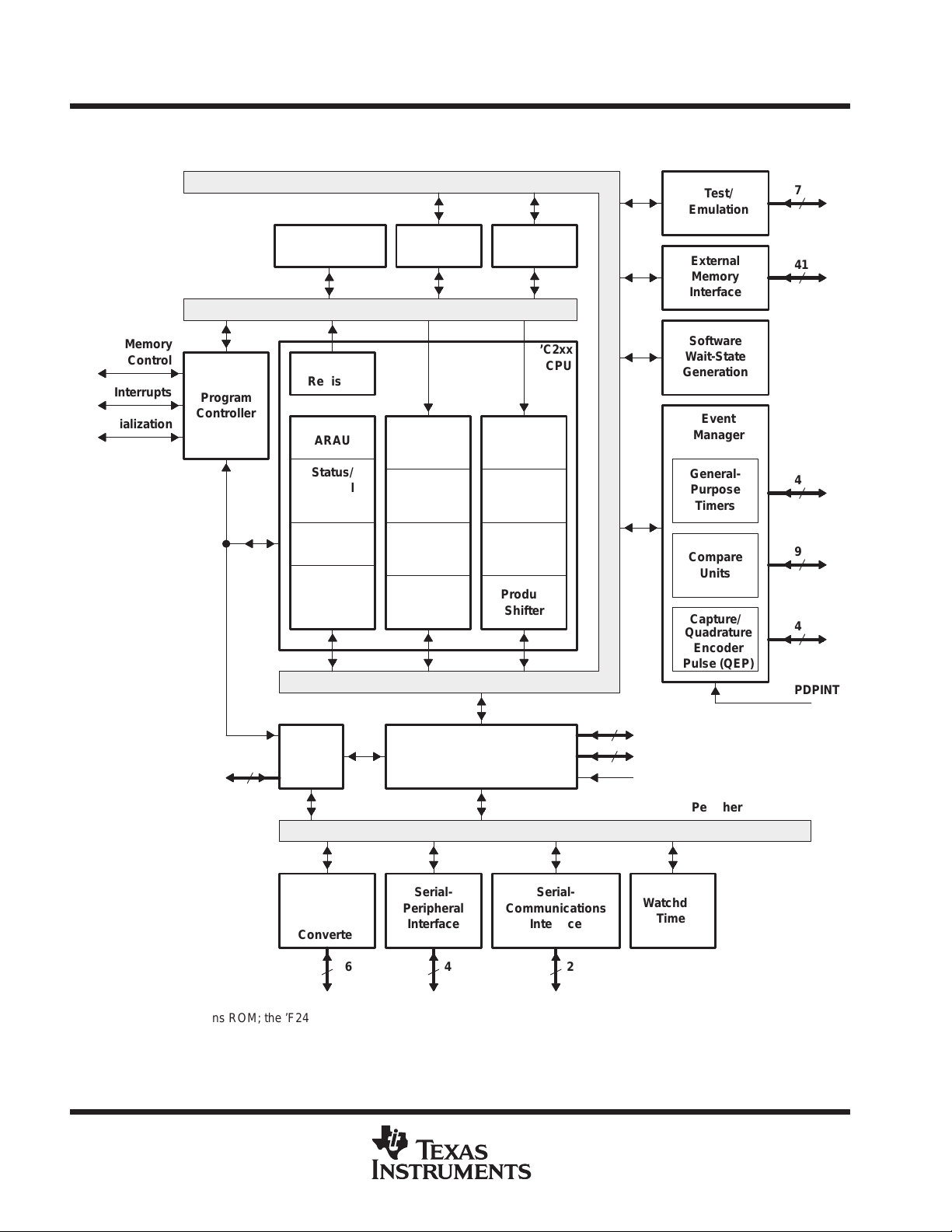
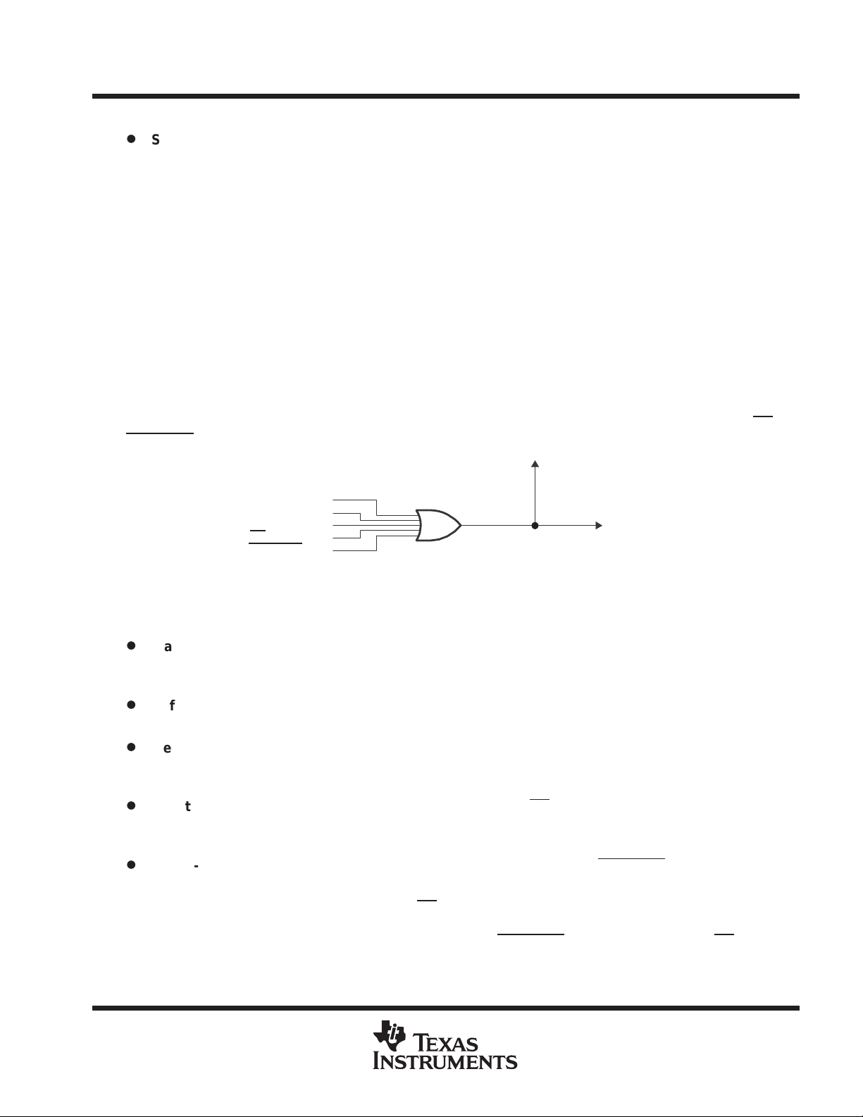
functional block diagram
Data Bus
Memory
Control
Interrupts
Initialization
Program Bus
Program
Controller
EEPROM
Instruction
Register
ARAU
Status/
Control
Registers
Auxiliary
Registers
Memory-
Mapped
Registers
†
DARAMROM or Flash
B0
Input
Shifter
ALU
Accumulator
Output
Shifter
DARAM
B1/B2
Multiplier
TREG
PREG
Product
Shifter
’C2xx
CPU
Test/
Emulation
External
Memory
Interface
Software
Wait-State
Generation
Event
Manager
General-
Purpose
Timers
Compare
Units
Capture/
Quadrature
Encoder
Pulse (QEP)
7
41
4
9
4
Clock
3
†
The ’C240 device contains ROM; the ’F240 device contains Flash EEPROM.
Module
Dual 10-Bit
Analog-
to-Digital
Converter
System-Interface
Module
Serial-
Peripheral
Interface
4
Serial-
Communications
Interface
216
4
Interrupts
20
Digital Input/Output
Reset
Watchdog
Timer
PDPINT
Peripheral Bus
12
POST OFFICE BOX 1443 • HOUSTON, TEXAS 77251–1443
(V)
(ns)
PIN COUNT
description (continued)
TMS320C240, TMS320F240
DSP CONTROLLERS
SPRS042D – OCTOBER 1996 – REVISED NOVEMBER 1998
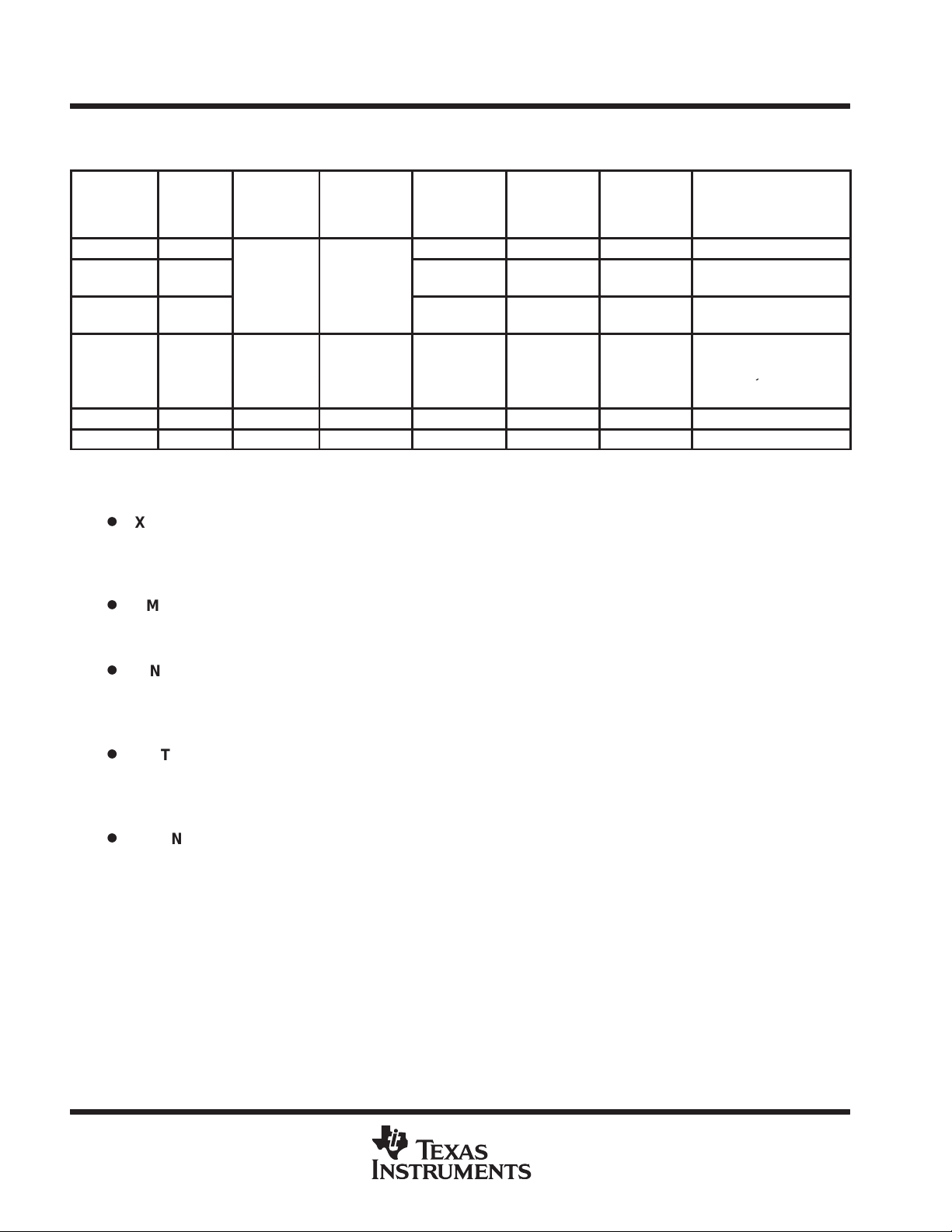
Table 1. Characteristics of the ’x240 DSP Controllers
ON-CHIP MEMORY (WORDS)
TMS320x240
DEVICES
DATA DATA/PROG PROG PROG
TMS320C240 288 256 16K – 5 50 PQ 132–P
TMS320F240 288 256 – 16K 5 50 PQ 132–P
RAM ROM
FLASH
EEPROM
POWER
SUPPLY
CYCLE
TIME
PACKAGE
TYPE
architectural overview
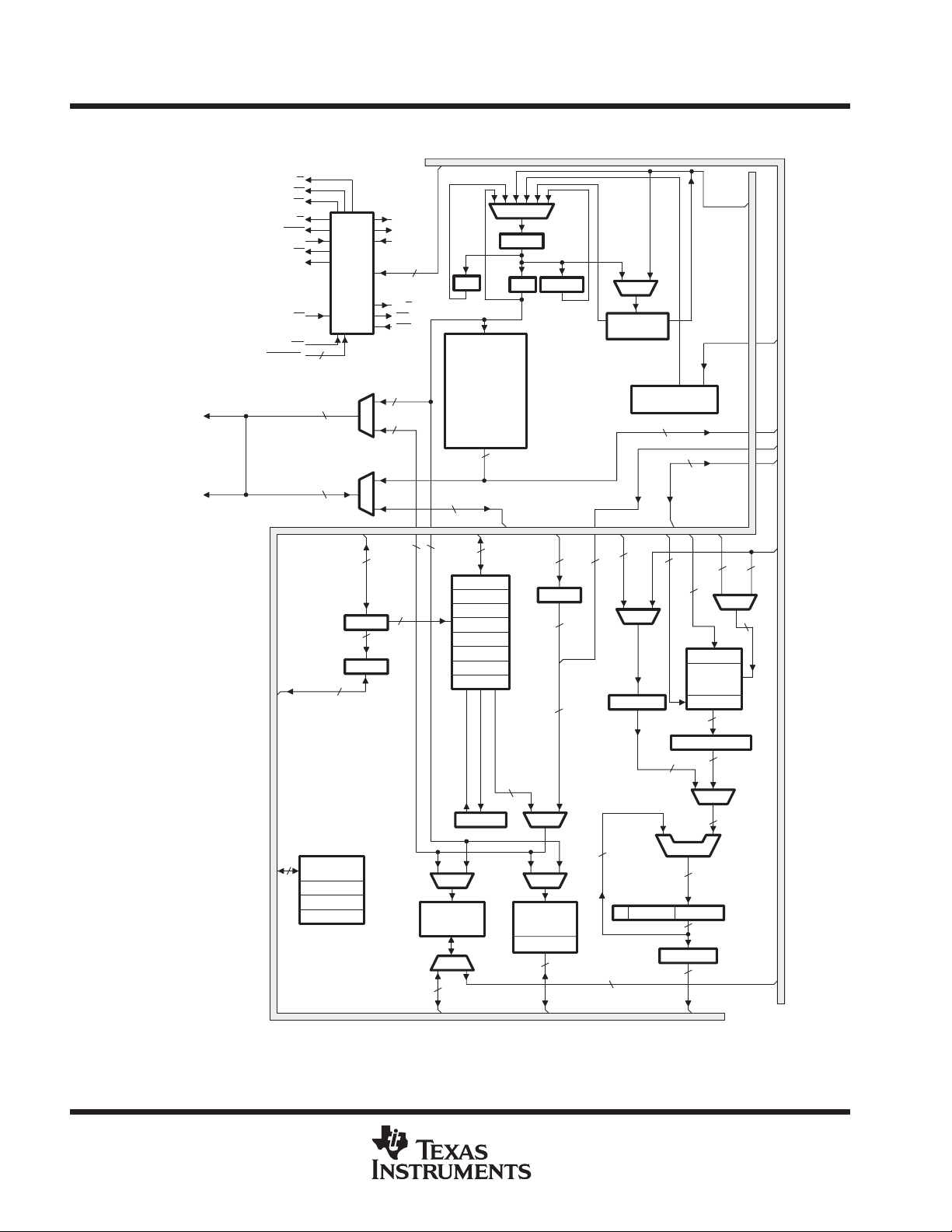
The functional block diagram provides a high-level description of each component in the ’x240 DSP controller.
The TMS320x240 devices are composed of three main functional units: a ’C2xx DSP core, internal memory,
and peripherals. In addition to these three functional units, there are several system-level features of the ’x240
that are distributed. These system features include the memory map, device reset, interrupts, digital
input/output (I/O), clock generation, and low-power operation.
system-level functions
device memory map
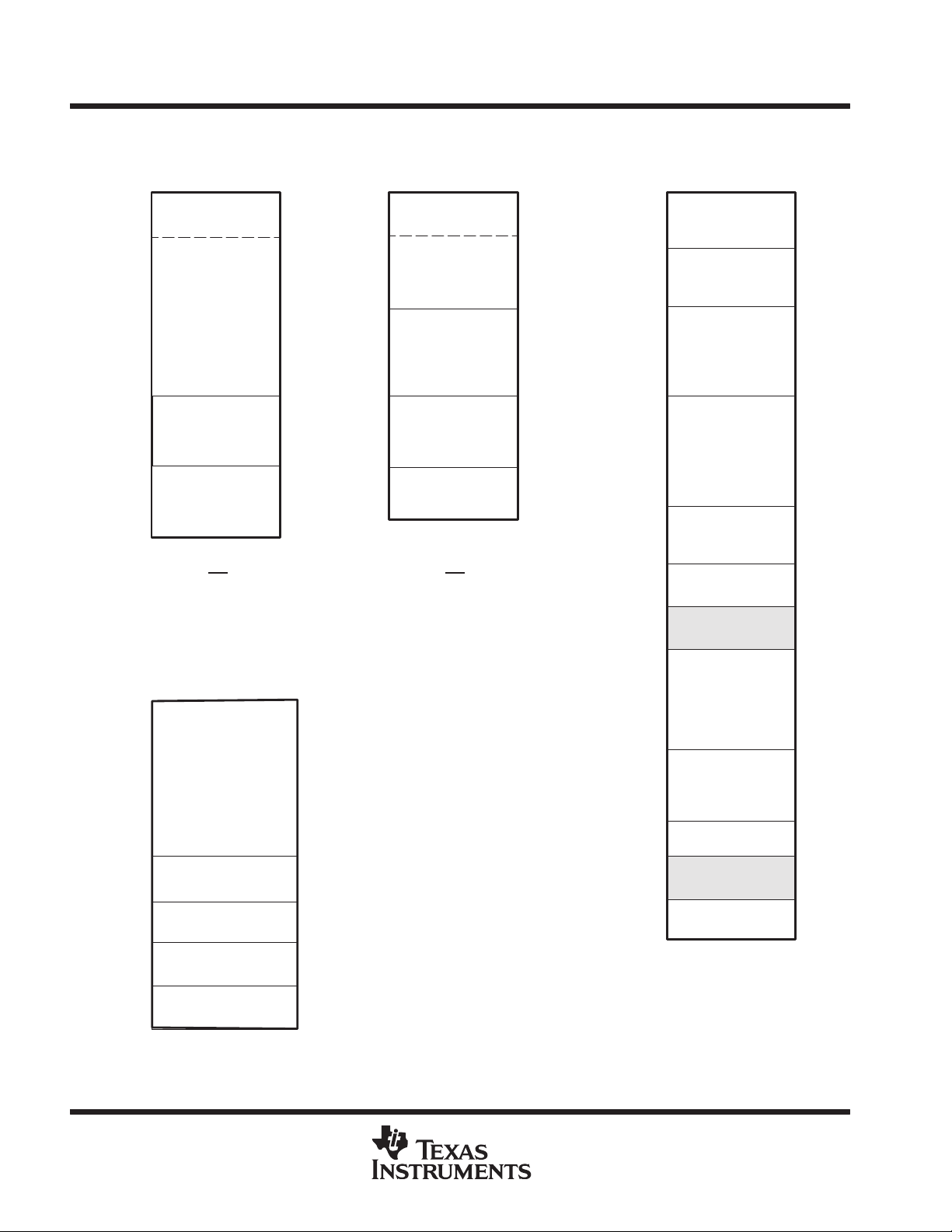
The TMS320x240 implements three separate address spaces for program memory, data memory, and I /O.
Each space accommodates a total of 64K 16-bit words. Within the 64K words of data space, the 256 to
32K words at the top of the address range can be defined to be external global memory in increments of powers
of two, as specified by the contents of the global memory allocation register (GREG). Access to global memory
is arbitrated using the global memory bus request (BR) signal.
On the ’x240, the first 96 (0–5Fh) data memory locations are either allocated for memory-mapped registers or
are reserved. This memory-mapped register space contains various control and status registers including those
for the CPU.
All the on-chip peripherals of the ’x240 device are mapped into data memory space. Access to these registers
is made by the CPU instructions addressing their data-memory locations. Figure 1 shows the memory map.
POST OFFICE BOX 1443 • HOUSTON, TEXAS 77251–1443
13
TMS320C240, TMS320F240
DSP CONTROLLERS
SPRS042D – OCTOBER 1996 – REVISED NOVEMBER 1998
device memory map (continued)
Program
Program
Data
Hex
0000
003F
0040
FDFF
FE00
On-Chip DARAM B0
External (CNF = 0)
FEFF
FF00
FFFF
Microprocessor
Hex
0000
FEFF
FF00
FF0E
FF0F
FF10
FFFE
FFFF
Wait-state Generator
Interrupts
(External)
External
(CNF = 1)
or
Reserved
= 1
MP/MC
Mode
I/O
External
Reserved
Flash Control
Mode Register
Reserved
Control Register
Hex
0000
003F
0040
3FFF
4000
FDFF
FE00
FEFF
FF00
FFFF
†
ROM/Flash memory includes
address range 0000h–003Fh
Interrupts
(On-Chip)
On-Chip ROM
(Flash EEPROM)
(8 x 2K Segments)
External
On-Chip DARAM B0
(CNF = 1)
External (CNF = 0)
Reserved
MP/MC = 0
Microcomputer
Mode
†
or
Hex
0000
005F
0060
007F
0080
01FF
0200
02FF
0300
03FF
0400
07FF
0800
6FFF
7000
73FF
7400
743F
7440
77FF
7800
7FFF
8000
FFFF
Memory-Mapped
Registers and
Reserved
On-Chip
DARAM B2
Reserved
On-Chip DARAM B0
(CNF = 0)
or
Reserved (CNF = 1)
On-Chip
DARAM B1
Reserved
Illegal
Peripheral Memory-
Mapped Registers
(System, WD,
ADC, SPI, SCI,
Interrupts, I/O)
Peripheral
Memory-Mapped
Registers
(Event Manager)
Reserved
Illegal
External
14
Figure 1. TMS320x240 Memory Map
POST OFFICE BOX 1443 • HOUSTON, TEXAS 77251–1443
TMS320C240, TMS320F240
DSP CONTROLLERS
SPRS042D – OCTOBER 1996 – REVISED NOVEMBER 1998
peripheral memory map
The TMS320x240 system and peripheral control register frame contains all the data, status, and control bits
to operate the system and peripheral modules on the device (excluding the event manager).
Hex
0000
0003
0004
0005
0006
0007
005F
Hex
0000
005F
0060
007F
0080
Memory-Mapped Registers
and Reserved
On-Chip DARAM B2
Reserved
Interrupt-Mask Register
Global-Memory Allocation
Register
Interrupt Flag Register
Emulation Registers
and Reserved
01FF
0200
02FF
0300
03FF
0400
07FF
0800
6FFF
7000
73FF
7400
743F
7440
77FF
7800
7FFF
8000
FFFF
Reserved
On-Chip DARAM
B0 (CNF = 0)
Reserved (CNF = 1)
On-Chip
DARAM B1
Reserved
Illegal
Peripheral Frame 1
Peripheral Frame 2
Reserved
Illegal
External
Illegal
System Configuration and
Control Registers
Watchdog Timer and
PLL Control Registers
ADC
SPI
SCI
Illegal
External-Interrupt Registers
Illegal
Digital-I/O Control Registers
Illegal
General-Purpose
Timer Registers
Reserved
Compare, PWM, and
Deadband Registers
Reserved
Capture & QEP Registers
Reserved
Interrupt Mask, Vector and
Flag Registers
Reserved
7000–700F
7010–701F
7020–702F
7030–703F
7040–704F
7050–705F
7060–706F
7070–707F
7080–708F
7090–709F
70A0–73FF
7400–740C
740D–7410
7411–741C
741D–741F
7420–7426
7427–742B
742C–7434
7435–743F
Figure 2. Peripheral Memory Map
POST OFFICE BOX 1443 • HOUSTON, TEXAS 77251–1443
15
TMS320C240, TMS320F240
DSP CONTROLLERS
SPRS042D – OCTOBER 1996 – REVISED NOVEMBER 1998
digital I/O and shared pin functions
The ’C240 has a total of 28 pins shared between primary functions and I/Os. These pins are divided into two
groups:
D
Group1 — Primary functions shared with I/Os belonging to dedicated I/O ports, Port A, Port B, and Port C.
D
Group2 — Primary functions belonging to peripheral modules which also have a built-in I/O feature as a
secondary function (for example, SCI, SPI, external interrupts, and PLL clock modules).
description of group1 shared I/O pins
The control structure for Group1 type shared I/O pins is shown in Figure 3. The only exception to this
configuration is the CLKOUT/IOPC1 pin. In Figure 3, each pin has three bits that define its operation:
D
Mux control bit — this bit selects between the primary function (1) and I/O function (0) of the pin.
D
I/O direction bit — if the I/O function is selected for the pin (mux control bit is set to 0), this bit determines
whether the pin is an input (0) or an output (1).
D
I/O data bit — if the I/O function is selected for the pin (mux control bit is set to 0) and the direction selected
is an input, data is read from this bit; if the direction selected is an output, data is written to this bit.
The mux control bit, I/O direction bit, and I/O data bit are in the I/O control registers.
IOP DIR Bit
0 = Input
1 = Output
IOP Data Bit
(Read/Write)
In Out
Figure 3. Shared Pin Configuration
Primary
Function
or I/O Pin
Primary
Function
01
Pin
Note:
When the MUX control bit = 1, the primary
function is selected in all cases except
for the following pins:
1. XF/IOPC2 (0 = Primary Function)
/IOPC3 (0 = Primary Function)
2. BIO
MUX Control Bit
0 = I/O Function
1 = Primary Function
A summary of Group1 pin configurations and associated bits is shown in Table 2.
16
POST OFFICE BOX 1443 • HOUSTON, TEXAS 77251–1443
PIN #
REGISTER
description of group1 shared I/O pins (continued)
Table 2. Group1 Shared Pin Configurations
TMS320C240, TMS320F240
DSP CONTROLLERS
SPRS042D – OCTOBER 1996 – REVISED NOVEMBER 1998
MUX CONTROL
(name.bit #)
72 OCRA.0 ADCIN0 IOPA0 PADATDIR 0 8
73 OCRA.1 ADCIN1 IOPA1 PADATDIR 1 9
90 OCRA.2 ADCIN9 IOPA2 PADATDIR 2 10
91 OCRA.3 ADCIN8 IOPA3 PADATDIR 3 11
100 OCRA.8 PWM7/CMP7 IOPB0 PBDATDIR 0 8
101 OCRA.9 PWM8/CMP8 IOPB1 PBDATDIR 1 9
102 OCRA.10 PWM9/CMP9 IOPB2 PBDATDIR 2 10
105 OCRA.11 T1PWM/T1CMP IOPB3 PBDATDIR 3 11
106 OCRA.12 T2PWM/T2CMP IOPB4 PBDATDIR 4 12
107 OCRA.13 T3PWM/T3CMP IOPB5 PBDATDIR 5 13
108 OCRA.14 TMRDIR IOPB6 PBDATDIR 6 14
109 OCRA.15 TMRCLK IOPB7 PBDATDIR 7 15
63 OCRB.0 ADCSOC IOPC0 PCDATDIR 0 8
64 SYSCR.7–6
0 0 IOPC1 PCDATDIR 1 9
0 1 WDCLK — — —
1 0 SYSCLK — — —
1 1 CPUCLK — — —
65 OCRB.2 IOPC2 XF PCDATDIR 2 10
66 OCRB.3 IOPC3 BIO PCDATDIR 3 11
67 OCRB.4 CAP1/QEP1 IOPC4 PCDATDIR 4 12
68 OCRB.5 CAP2/QEP2 IOPC5 PCDATDIR 5 13
69 OCRB.6 CAP3 IOPC6 PCDATDIR 6 14
70 OCRB.7 CAP4 IOPC7 PCDATDIR 7 15
†
Valid only if the I/O function is selected on the pin.
PIN FUNCTION SELECTED I/O PORT DATA AND DIRECTION
(CRx.n = 1) (CRx.n = 0) REGISTER DATA BIT # DIR BIT #
†
POST OFFICE BOX 1443 • HOUSTON, TEXAS 77251–1443
17
TMS320C240, TMS320F240
DSP CONTROLLERS
SPRS042D – OCTOBER 1996 – REVISED NOVEMBER 1998
description of group2 shared I/O pins
Group2 shared pins belong to peripherals that have built-in general-purpose I/O capability. Control and
configuration for these pins are achieved by setting the appropriate bits within the control and configuration
registers of the peripherals. Table 3 lists the Group2 shared pins.
Table 3. Group2 Shared Pin Configurations
PIN # PRIMARY FUNCTION REGISTER ADDRESS PERIPHERAL MODULE
43 SCIRXD SCIPC2 705Eh SCI
44 SCITXD SCIPC2 705Eh SCI
45 SPISIMO SPIPC2 704Eh SPI
48 SPISOMI SPIPC2 704Eh SPI
49 SPICLK SPIPC1 704Dh SPI
51 SPISTE SPIPC1 704Dh SPI
54 XINT2 XINT2CR 7078h External Interrupts
55 XINT3 XINT3CR 707Ah External Interrupts
digital I/O control registers
Table 4 lists the registers available to the digital I/O module. As with other ’x240 peripherals, the registers are
memory-mapped to the data space.
Table 4. Addresses of Digital I/O Control Registers
ADDRESS REGISTER NAME
7090h OCRA I/O mux control register A
7092h OCRB I/O mux control register B
7098h PADATDIR I/O port A data and direction register
709Ah PBDATDIR I/O port B data and direction register
709Ch PCDATDIR I/O port C data and direction register
device reset and interrupts
The TMS320x240 software-programmable interrupt structure supports flexible on-chip and external interrupt
configurations to meet real-time interrupt-driven application requirements. The ’x240 recognizes three types of
interrupt sources:
D
Reset (hardware- or software-initiated) is unarbitrated by the CPU and takes immediate priority over any
other executing functions. All maskable interrupts are disabled until the reset service routine enables them.
D
Hardware-generated interrupts are requested by external pins or by on-chip peripherals. There are two
types:
–
External interrupts
are generated by one of five external pins corresponding to the interrupts XINT1,
XINT2, XINT3, PDPINT , and NMI. The first four can be masked both by dedicated enable bits and by t he
CPU’ s interrup t mask regi ster (IMR ), which c an mask ea ch maskab le interr upt line a t the DSP cor e. NMI,
which is not maskable, takes priority over peripheral interrupts and software-generated interrupts. It can
be locked out only by an already executing NMI or a reset.
18
–
Peripheral interrupts
are initiated internally by these on-chip peripheral modules: the event manager,
SPI, SCI, watchdog/real-time interrupt (WD/RTI), and ADC. They can be masked both by enable bits
for each event in each peripheral and by the CPU’s IMR, which can mask each maskable interrupt line at
the DSP core.
POST OFFICE BOX 1443 • HOUSTON, TEXAS 77251–1443
device reset and interrupts (continued)
D
Software-generated interrupts for the ’x240 device include:
TMS320C240, TMS320F240
DSP CONTROLLERS
SPRS042D – OCTOBER 1996 – REVISED NOVEMBER 1998
The INTR instruction.
–
This instruction allows initialization of any ’x240 interrupt with software. Its
operand indicates to which interrupt vector location the CPU branches. This instruction globally
disables maskable interrupts (sets the INTM bit to 1).
–
The NMI instruction.
This instruction forces a branch to interrupt vector location 24h, the same location
used for the nonmaskable hardware interrupt NMI. NMI can be initiated by driving the NMI pin low or by
executing an NMI instruction. This instruction globally disables maskable interrupts.
–
The TRAP instruction.
TRAP instruction does
This instruction forces the CPU to branch to interrupt vector location 22h. The
not
disable maskable interrupts (INTM is not set to 1); therefore, when the CPU
branches to the interrupt service routine, that routine can be interrupted by the maskable hardware
interrupts.
–
An emulator trap.
This interrupt can be generated with either an INTR instruction or a TRAP instruction.
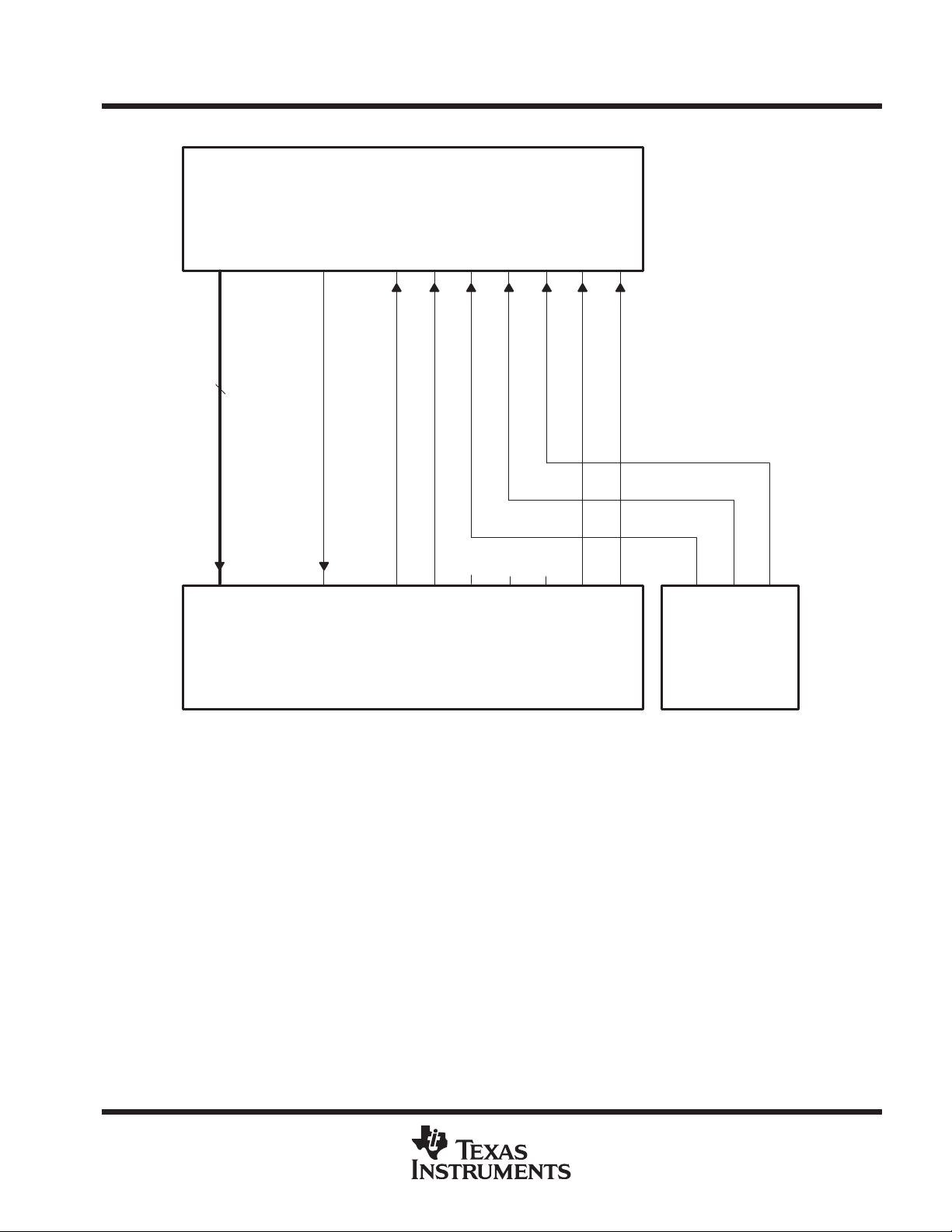
reset
The reset operation ensures an orderly startup sequence for the device. There are five possible causes of a
reset, as shown in Figure 4. Three of these causes are internally generated; the other two causes, the RS and
PORESET pins, are controlled externally.
To Device
Watchdog Timer Reset
Software-Generated Reset
Illegal Address Reset
Power-On Reset (PORESET
Reset (RS
) Pin Active
) Pin
Active
Reset
Signal
To Reset Out
Figure 4. Reset Signals
The five possible reset signals are generated as follows:
D
Watchdog timer reset. A watchdog-timer-generated reset occurs if the watchdog timer overflows or an
improper value is written to either the watchdog key register or the watchdog control register. (Note that
when the device is powered on, the watchdog timer is automatically active.)
D
Software-generated reset. This is implemented with the system control register (SYSCR). Clearing the
RESET0 bit (bit 14) or setting the RESET1 bit (bit 15) causes a system reset.
D
Illegal address reset. The system and peripheral module control register frame address map contains
unimplemented address locations in the ranges labeled illegal. Any access to an address located in the
Illegal ranges generate an illegal-address reset.
D
Reset pin active. To generate an external reset pulse on the RS pin, a low-level pulse duration of as little
as a few nanoseconds is usually effective; however , pulses of one SYSCLK cycle are necessary to ensure
that the device recognizes the reset signal.
D
Power-on reset pin active. To generate a power-on reset pulse on the PORESET pin, a low-level pulse
of one SYSCLK cycle is necessary to ensure that the device recognizes the reset signal.
Once a reset source is activated, the external RS
pin is driven (active) low for a minimum of eight SYSCLK
cycles. This allows the TMS320x240 device to reset external system components. Additionally , if a brown-out
condition (VCC < VCCmin for several microseconds causing PORESET to go low) occurs or the RS pin is held
low, then the reset logic holds the device in a reset state for as long as these actions are active.
POST OFFICE BOX 1443 • HOUSTON, TEXAS 77251–1443
19
TMS320C240, TMS320F240
DSP CONTROLLERS
SPRS042D – OCTOBER 1996 – REVISED NOVEMBER 1998
reset (continued)
The occurrence of a reset condition causes the TMS320x240 to terminate program execution and affects
various registers and status bits. During a reset, RAM contents remain unchanged, and all control bits that are
affected by a reset are initialized to their reset state. In the case of a power-on reset, the PLL control registers
are initialized to zero. The program needs to recognize power-on resets and configure the PLL for correct
operation.
After a reset, the program can check the power-on reset flag (PORST flag, SYSSR.15), the illegal address flag
(ILLADR flag, SYSSR.12), the software reset flag (SWRST flag, SYSSR.10), and the watchdog reset flag
(WDRST flag, SYSSR.9) to determine the source of the reset. A reset does not clear these flags.
RS
and PORESET must be held low until the clock signal is valid and VCC is within the operating range. In
addition, PORESET must be driven low when VCC drops below the minimum operating voltage.
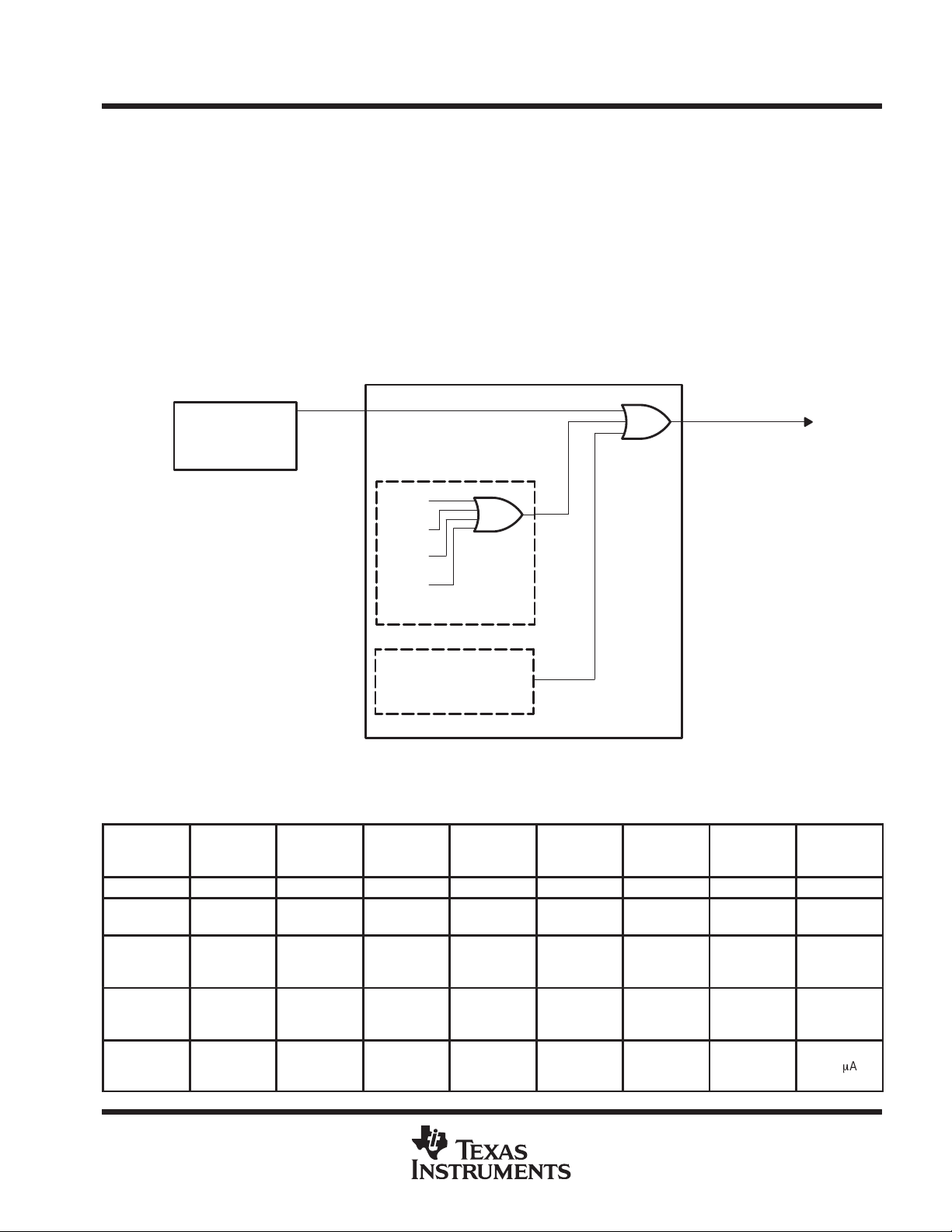
hardware-generated interrupts
All the hardware interrupt lines of the DSP core are given a priority rank from 1 to 10 (1 being highest). When
more than one of these hardware interrupts is pending acknowledgment, the interrupt of highest rank gets
acknowledged first. The others are acknowledged in order after that. Of those ten lines, six are for maskable
interrupt lines (INT1–INT6) and one is for the nonmaskable interrupt (NMI) line. INT1–INT6 and NMI have the
priorities shown in Table 5.
Table 5. Interrupt Priorities at the Level of the DSP Core
INTERRUPT
RESET 1
TI RESERVED
NMI 3
INT1 4
INT2 5
INT3 6
INT4 7
INT5 8
INT6 9
TI RESERVED
†
TI Reserved means that the address space is
reserved for Texas Instruments.
†
†
PRIORITY AT THE
DSP CORE
2
10
The inputs to these lines are controlled by the system module and the event manager as summarized in T able 6
and shown in Figure 5.
Table 6. Interrupt Lines Controlled by the System Module and Event Manager
PERIPHERAL INTERRUPT LINES
INT1
System Module
Event Manager
INT5
INT6
INT2
INT3
INT4
NMI
20
POST OFFICE BOX 1443 • HOUSTON, TEXAS 77251–1443
hardware-generated interrupts (continued)
DSP Core
TMS320C240, TMS320F240
DSP CONTROLLERS
SPRS042D – OCTOBER 1996 – REVISED NOVEMBER 1998
Address
Lines 5–1
5
Address
Lines 5–1
IACK
INT6 INT5 INT4 INT3 INT2 INT1 NMI
NC NC NC
INT6 INT5 INT4 INT3 INT2 INT1 NMIIACK
System Module Event Manager
INTC INTB INTA
Figure 5. DSP Interrupt Structure
At the level of the system module and the event manager, each of the maskable interrupt lines (INT1–INT6) is
connected to multiple maskable interrupt sources. Sources connected to interrupt line INT1 are called Level 1
interrupts; sources connected to interrupt line INT2 are called Level 2 interrupts; and so on. For each interrupt
line, the multiple sources also have a set priority ranking. The source with the highest priority has its interrupt
request responded to by the DSP core first.
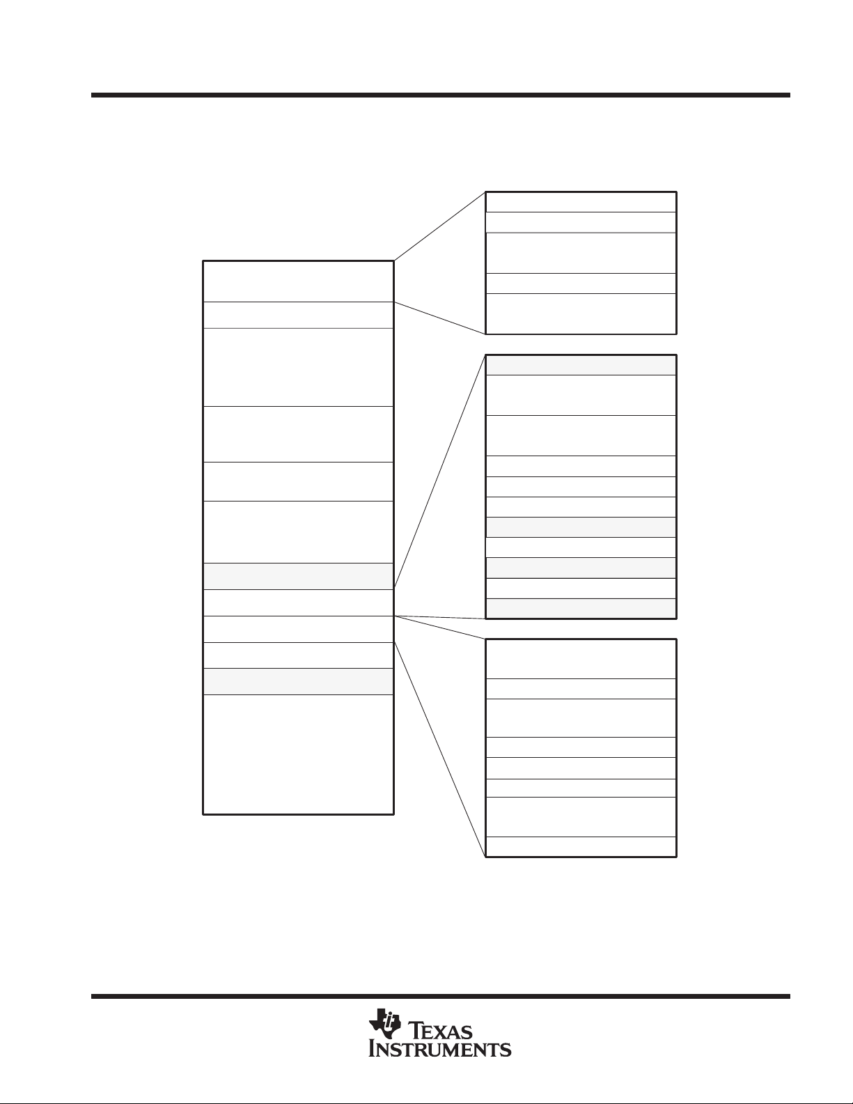
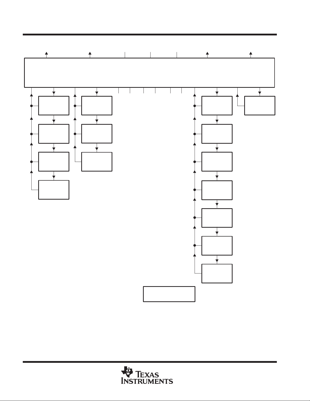
Figure 6 shows the sources and priority ranking for the interrupts controlled by the system module. For each
interrupt chain, the interrupt source of highest priority is at the top. Priority decreases from the top of the chain
to the bottom. Figure 7 shows the interrupt sources and priority ranking for the event manager interrupts.
POST OFFICE BOX 1443 • HOUSTON, TEXAS 77251–1443
21
TMS320C240, TMS320F240
DSP CONTROLLERS
SPRS042D – OCTOBER 1996 – REVISED NOVEMBER 1998
hardware-generated interrupts (continued)
To DSP INT6 To DSP INT1 To DSP NMI
To DSP INT5
NCNCNC
Dual ADC
Interrupt
System-Module
External Interrupt
XINT1
(low priority)
System-Module
External Interrupt
XINT2
(low priority)
System-Module
External Interrupt
XINT3
(low priority)
INT5
SPI
Interrupt
(low priority)
SCI
Receiver
Interrupt
(low priority)
SCI
Transmitter
Interrupt
(low priority)
System Module
INT2INT3INT4
IACK1IRQ1IACK5IRQ5IACK6IRQ6
NCNCNCNCNCNC
System-Module
External Interrupt
XINT1
(high priority)
System-Module
External Interrupt
XINT2
(high priority)
System-Module
External Interrupt
XINT3
(high priority)
Watchdog
Timer
Interrupt
NMIINT1INT6
IACK_NMIIRQ_NMIIACK2IRQ2IACK3IRQ3IACK4IRQ4
System-Module
External Interrupt
NMI
Legend:
NC = No connection
IACK = interrupt acknowledge
IRQ = interrupt request
Figure 6. System-Module Interrupt Structure
SPI
Interrupt
(high priority)
SCI
Receiver
Interrupt
(high priority)
SCI
Transmitter
Interrupt
(high priority)
22
POST OFFICE BOX 1443 • HOUSTON, TEXAS 77251–1443
hardware-generated interrupts (continued)
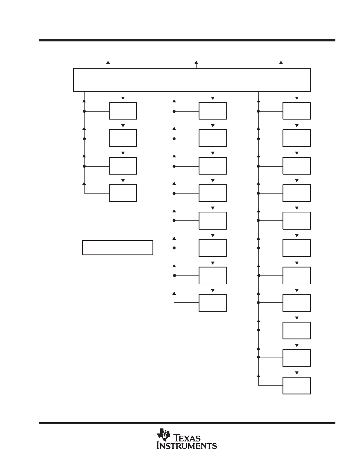
To DSP INT4 To DSP INT3 To DSP INT2
TMS320C240, TMS320F240
DSP CONTROLLERS
SPRS042D – OCTOBER 1996 – REVISED NOVEMBER 1998
INTAINTBINTC
Event Manager
IACKAIRQAIACKBIRQBIACKCIRQC
Legend:
Capture 1
Interrupt
Capture 2
Interrupt
Capture 3
Interrupt
Capture 4
Interrupt
IACK = Interrupt acknowledge
IRQ = Interrupt request
Timer 2
Period
Interrupt
Timer 2
Compare
Interrupt
Timer 2
Underflow
Interrupt
Timer 2
Overflow
Interrupt
Timer 3
Period
Interrupt
Timer 3
Compare
Interrupt
Timer 3
Underflow
Interrupt
Power-Drive
Protection
Interrupt
Compare1
Interrupt
Compare 2
Interrupt
Compare 3
Interrupt
Simple-
Compare 1
Interrupt
Simple-
Compare 2
Interrupt
Simple-
Compare 3
Interrupt
Timer 3
Overflow
Interrupt
Figure 7. Event-Manager Interrupt Structure
POST OFFICE BOX 1443 • HOUSTON, TEXAS 77251–1443
Timer 1
Period
Interrupt
Timer 1
Compare
Interrupt
Timer 1
Underflow
Interrupt
Timer 1
Overflow
Interrupt
23

TMS320C240, TMS320F240
DSP CONTROLLERS
SPRS042D – OCTOBER 1996 – REVISED NOVEMBER 1998
hardware-generated interrupts (continued)
Each of the interrupt sources has its own control register with a flag bit and an enable bit. When an interrupt
request is received, the flag bit in the corresponding control register is set. If the enable bit is also set, a signal
is sent to arbitration logic, which can simultaneously receive similar signals from one or more of the other control
registers. The arbitration logic compares the priority level of competing interrupt requests, and it passes the
interrupt of highest priority to the CPU. The corresponding flag is set in the interrupt flag register (IFR), indicating
that the interrupt is pending. The CPU then must decide whether to acknowledge the request. Maskable
hardware interrupts are acknowledged only after certain conditions are met:
D
Priority is highest. When more than one hardware interrupt is requested at the same time, the ’x240
services them according to the set priority ranking.
D
INTM bit is 0. The interrupt mode (INTM) bit, bit 9 of status register ST0, enables or disables all maskable
interrupts:
– When INTM = 0, all unmasked interrupts are enabled.
– When INTM = 1, all unmasked interrupts are disabled.
INTM is set to 1 automatically when the CPU acknowledges an interrupt (except when initiated by the TRAP
instruction) and at reset. It can be set and cleared by software.
D
IMR mask bit is 1. Each of the maskable interrupt lines has a mask bit in the interrupt mask register (IMR).
To unmask an interrupt line, set its IMR bit to 1.
When the CPU acknowledges a maskable hardware interrupt, it jams the instruction bus with the INTR
instruction. This instruction forces the PC to the appropriate address from which the CPU fetches the software
vector. This vector leads to an interrupt service routine.
Usually, the interrupt service routine reads the peripheral-vector-address offset from the peripheral-vectoraddress register (see Table 7) to branch to code that is meant for the specific interrupt source that initiated the
interrupt request. The ’x240 includes a phantom-interrupt vector offset (0000h), which is a system interrupt
integrity feature that allows a controlled exit from an improper interrupt sequence. If the CPU acknowledges a
request from a peripheral when, in fact, no peripheral has requested an interrupt, the phantom-interrupt vector
is read from the interrupt-vector register.
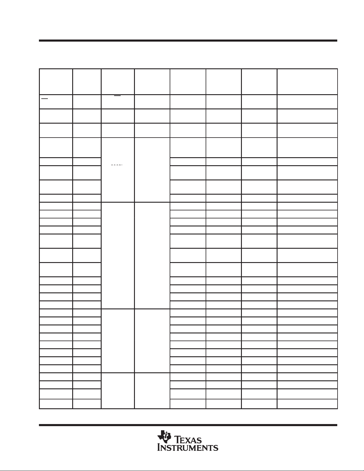
Table 7 summarizes the interrupt sources, overall priority, vector address/offset, source, and function of each
interrupt available on the TMS320x240.
24
POST OFFICE BOX 1443 • HOUSTON, TEXAS 77251–1443
(System)
0004h
0006h
M
Grou B)
M
hardware-generated interrupts (continued)
Table 7. ’x240 Interrupt Locations and Priorities
TMS320C240, TMS320F240
DSP CONTROLLERS
SPRS042D – OCTOBER 1996 – REVISED NOVEMBER 1998
INTERRUPT
NAME
RS
RESERVED 2
NMI 3
XINT1
XINT2
XINT3
SPIINT 7
RXINT 8
TXINT 9
WDTINT 10 0010h Y WDT Watchdog timer interrupt
PDPINT 11 0020h Y External Power-drive protection Int.
CMP1INT 12 0021h Y EV.CMP1 Full Compare 1 interrupt
CMP2INT 13 0022h Y EV.CMP2 Full Compare 2 interrupt
CMP3INT 14 0023h Y EV.CMP3 Full Compare 3 interrupt
SCMP1INT 15
SCMP2INT 16
SCMP3INT 17
TPINT1 18 0027h Y EV.GPT1 Timer1-period interrupt
TCINT1 19 0028h Y EV.GPT1 Timer1-compare interrupt
TUFINT1 20 0029h Y EV.GPT1 Timer1-underflow interrupt
TOFINT1 21 002Ah Y EV.GPT1 T imer1-overflow interrupt
TPINT2 22 002Bh Y EV.GPT2 T imer2-period interrupt
TCINT2 23
TUFINT2 24
TOFINT2 25
TPINT3 26
TCINT3 27
TUFINT3 28
TOFINT3 29 0032h Y EV.GPT3 Timer3-overflow interrupt
CAPINT1 30 INT4 0033h Y EV.CAP1 Capture 1 interrupt
CAPINT2 31 0008h
CAPINT3 32
CAPINT4 33
OVERALL
PRIORITY
1
Highest
4
5
6
DSP-CORE
INTERRUPT,
AND
ADDRESS
RS
0000h
INT7
0026h
NMI
0024h
INT1
0002h
INT2
(Event
Manager
Group A)
INT3
(Event
anager
p
(Event
anager
Group C)
PERIPHERAL
VECTOR
ADDRESS
N/A N Core, SD
N/A N/A N DSP Core Emulator trap
N/A 0002h N Core, SD External user interrupt
SYSIVR
(701Eh)
EVIVRA
(7432h)
EVIVRB
(7433h)
EVIVRC
(7434h)
PERIPHERAL
VECTOR
ADDRESS
OFFSET
0001h
0011h
001Fh
0005h Y SPI High-priority SPI interrupt
0006h Y SCI
0007h Y SCI
0024h Y EV.CMP4
0025h Y EV.CMP5
0026h Y EV.CMP6
002Ch Y EV.GPT2 Timer2-compare interrupt
002Dh Y EV.GPT2 Timer2-underflow interrupt
002Eh Y EV.GPT2 T imer2-overflow interrupt
002Fh Y EV.GPT3 Timer3-period interrupt
0030h Y EV.GPT3 Timer3-compare interrupt
0031h Y EV.GPT3 Timer3-underflow interrupt
0034h Y EV.CAP2 Capture 2 interrupt
0035h Y EV.CAP3 Capture 3 interrupt
0036h Y EV.CAP4 Capture 4 interrupt
MASKABLE?
Y SD
’x240
SOURCE
PERIPHERAL
MODULE
FUNCTION
INTERRUPT
External, system reset
(RESET)
High-priority external user
interrupts
SCI receiver interrupt
(high priority)
SCI transmitter interrupt
(high priority)
Simple compare 1
interrupt
Simple compare 2
interrupt
Simple compare 3
interrupt
POST OFFICE BOX 1443 • HOUSTON, TEXAS 77251–1443
25
TMS320C240, TMS320F240
SYSIVR
XINT2
39
(701Eh)
0011h
Y
y
DSP CONTROLLERS
SPRS042D – OCTOBER 1996 – REVISED NOVEMBER 1998
hardware-generated interrupts (continued)
Table 7. ’x240 Interrupt Locations and Priorities (Continued)
INTERRUPT
NAME
SPIINT 34 INT5
RXINT 35
TXINT 36
ADCINT 37 INT6 SYSIVR 0004h Y ADC Analog-to-digital interrupt
XINT1
XINT3
RESERVED 41 000Eh N/A Y DSP Core Used for analysis
TRAP N/A 0022h N/A N/A TRAP instruction vector
OVERALL
PRIORITY
38
40
DSP-CORE
INTERRUPT,
AND
ADDRESS
000Ah
(System)
000Ch
(System)
PERIPHERAL
VECTOR
ADDRESS
(701Eh)
PERIPHERAL
VECTOR
ADDRESS
OFFSET
0005h Y SPI Low-priority SPI interrupt
0006h Y SCI
0007h Y SCI
0001h
001Fh
MASKABLE?
Y
Y
’x240
SOURCE
PERIPHERAL
MODULE
External Low-priority external
pins
FUNCTION
INTERRUPT
SCI receiver interrupt
(low priority)
SCI transmitter interrupt
(low priority)
user interrupts
external interrupts
The ’x240 has five external interrupts. These interrupts include:
D
XINT1. Type A interrupt. The XINT1 control register (at 7070h) provides control and status for this interrupt.
XINT1 can be used as a high-priority (Level 1) or low-priority (Level 6) maskable interrupt or as a
general-purpose input pin. XINT1 can also be programmed to trigger an interrupt on either the rising or the
falling edge.
D
NMI. T ype A inter rupt. The NMI control register (at 7072h) provides control and status for this interrupt. NMI
is a nonmaskable external interrupt or a general-purpose input pin. NMI can also be programmed to trigger
an interrupt on either the rising or the falling edge.
D
XINT2. Type C interrupt. The XINT2 control register (at 7078h) provides control and status for this interrupt.
XINT2 can be used as a high-priority (Level 1) or low-priority (Level 6) maskable interrupt or a
general-purpose I/O pin. XINT2 can also be programmed to trigger an interrupt on either the rising or the
falling edge.
D
XINT3. Type C interrupt. The XINT3 control register (at 707Ah) provides control and status for this interrupt.
XINT3 can be used as a high-priority (Level 1) or low-priority (Level 6) maskable interrupt or as a
general-purpose I/O pin. XINT3 can also be programmed to trigger an interrupt on either the rising or the
falling edge.
D
PDPINT. This interrupt is provided for safe operation of the power converter and motor drive. This maskable
interrupt can put the timers and PWM output pins in the high-impedance state and inform the CPU in case
of motor drive abnormalities such as overvoltage, overcurrent, and excessive temperature rise. PDP IN T is
a Level 2 interrupt.
26
POST OFFICE BOX 1443 • HOUSTON, TEXAS 77251–1443
external interrupts (continued)
Table 8 is a summary of the external interrupt capability of the ’x240.
Table 8. External Interrupt Types and Functions
TMS320C240, TMS320F240
DSP CONTROLLERS
SPRS042D – OCTOBER 1996 – REVISED NOVEMBER 1998
EXTERNAL
INTERRUPT
XINT1 XINT1CR 7070h A No Input only
NMI NMICR 7072h A Yes Input only No
XINT2 XINT2CR 7078h C No I/O
XINT3 XINT3CR 707Ah C No I/O
PDPINT EVIMRA 742Ch N/A N/A N/A
CONTROL
REGISTER
NAME
CONTROL
REGISTER
ADDRESS
INTERRUPT
TYPE
CAN DO
NMI?
DIGITAL
I/O PIN
MASKABLE?
(Level 1 or 6)
(Level 1 or 6)
(Level 1 or 6)
clock generation
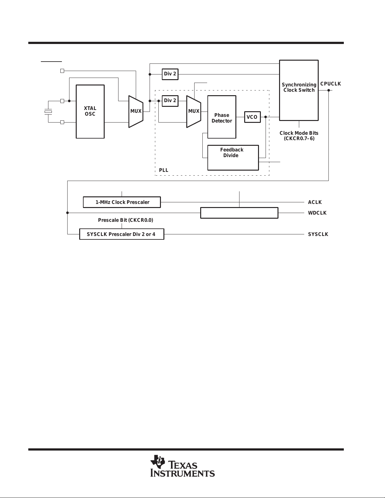
The TMS320x240 has an on-chip, PLL-based clock module. This module provides all the necessary clocking
signals for the device, as well as control for low-power mode entry . The only external component necessary for
this module is an external fundamental crystal, or oscillator.
The PLL-based clock module provides two basic modes of operation: oscillator mode and clock-in mode.
D
oscillator mode
This mode allows the use of a 4-, 6-, or 8-MHz external reference crystal to provide the time base to the
device. The internal oscillator circuitry is initialized by software to select the desired CPUCLK frequency,
which can be the input clock frequency , the input clock frequency divided by 2 (default), or a clock frequency
determined by the PLL.
Yes
Yes
Yes
Yes
(Level 2)
D
Clock-in mode
This mode allows the internal crystal oscillator circuitry to be bypassed. The device clocks are generated
from an external clock source input on the XTAL1/CLKIN pin. The device can be configured by software
to operate on the input clock frequency, the input clock frequency divided by 2, or a clock frequency
determined by the PLL.
The ’x240 runs on two clock frequencies: the CPU clock (CPUCLK) frequency , and the system clock (SYSCLK)
frequency . The CPU, memories, external memory interface, and event manager run at the CPUCLK frequency .
All other peripherals run at the SYSCLK frequency . The CPUCLK runs at 2x or 4x the frequency of the SYSCLK;
for example, for 2x, CPUCLK = 20 MHz and SYSCLK = 10 MHz. There is also a clock for the watchdog timer,
WDCLK. This clock has a nominal frequency of 16384 Hz (214 Hz) when XTAL1/CLKIN is a power of two or
a sum of two powers of two; for example, 4194304 Hz (222 Hz), 6291456 (222 + 221 Hz), or 8388608 Hz
(223 Hz).
The clock module includes three external pins:
1. XTAL1/CLKIN clock source/crystal input
2. XTAL2 output to crystal
3. OSCBYP oscillator bypass
For the external pins, if OSCBYP ≥ VIH, then the oscillator is enabled and if OSCBYP ≤ VIL, then the oscillator
is bypassed and the device is in clock-in mode. In clock-in mode, an external TTL clock must be applied to the
XTAL1/CLKIN pin. The XTAL2 pin can be left unconnected.
POST OFFICE BOX 1443 • HOUSTON, TEXAS 77251–1443
27
TMS320C240, TMS320F240
DSP CONTROLLERS
SPRS042D – OCTOBER 1996 – REVISED NOVEMBER 1998
clock generation (continued)
OSCBYP
XTAL1/CLKIN
XTAL
OSC
XTAL2
Clock Frequency and PLL Multiply Bits (CKCR1.7–4)
PLL
Div 2
Div 2
PLL divide-by-2 bit
(CKCR1.3)
MUXMUX
Phase
Detector
Feedback
Divider
Div 1, 2, 3, 4, 5,
or 9
VCO
Synchronizing
Clock Switch
Clock Mode Bits
(CKCR0.7–6)
PLL multiply ratio
(CKCR1.2–0)
CPUCLK
1-MHz Clock Prescaler
Prescale Bit (CKCR0.0)
SYSCLK Prescaler Div 2 or 4
Figure 8. PLL Clock Module Block Diagram
Watchdog Clock Prescaler
ACLK
WDCLK
SYSCLK
28
POST OFFICE BOX 1443 • HOUSTON, TEXAS 77251–1443
TMS320C240, TMS320F240
DSP CONTROLLERS
SPRS042D – OCTOBER 1996 – REVISED NOVEMBER 1998
low-power modes
The TMS320x240 has four low-power modes (idle 1, idle 2, PLL power down, and oscillator power down). The
low-power modes reduce the operating power by reducing or stopping the activity of various modules (by
stopping their clocks). The two PLLPM bits of the clock module control register, CKCR0, select which of the
low-power modes the device enters when executing an IDLE instruction. Reset or an unmasked interrupt from
any source causes the device to exit from idle 1 low-power mode. A real-time interrupt from the watchdog timer
module causes the device to exit from all low-power modes except oscillator power down. This is a wake-up
interrupt. When enabled, reset or any of the four external interrupts (NMI, XINT1, XINT2, or XINT3) causes the
device to exit from any of the low-power modes (idle 1, idle 2, PLL power down, and oscillator power down).
The external interrupts are all wake-up interrupts. The maskable external interrupts (XINT1, XINT2, and XINT3)
must be enabled individually and globally to bring the device out of a low-power mode properly . It is, therefore,
important to ensure that the desired low-power-mode exit path is enabled before entering a low-power mode.
Figure 9 shows the wake-up sequence from a power down. Table 9 summarizes the low-power modes.
Watchdog Timer
and
Real-Time Interrupt
Module
Wake-up
Signal
Wake-up Signal
to CPU
NMI
XINT1
XINT2
XINT3
External-Interrupt Logic
Reset
Signal
Reset Logic
System Module
Figure 9. Waking Up the Device From Power Down
Table 9. Low-Power Modes
LOW-
POWER
MODE
Run XX On On On On On – 80 mA
Idle 1 00 Off On On On On
Idle 2 01 Off Off On On On
PLL Power
Down
OSC Power
Down
PLLPM(x)
BITS IN
CKCR0[2:3]
10 Off Off On Off On
11 Off Off Off Off Off
CPUCLK
STATUS
SYSCLK
STATUS
WDCLK
STATUS
PLL
STATUS
OSC
STATUS
EXIT
CONDITION
Any interrupt
or reset
Wake-up
interrupt or
reset
Wake-up
interrupt or
reset
Wake-up
interrupt or
reset
TYPICAL
POWER
50 mA
7 mA
1 mA
400 mA
POST OFFICE BOX 1443 • HOUSTON, TEXAS 77251–1443
29
TMS320C240, TMS320F240
DSP CONTROLLERS
SPRS042D – OCTOBER 1996 – REVISED NOVEMBER 1998
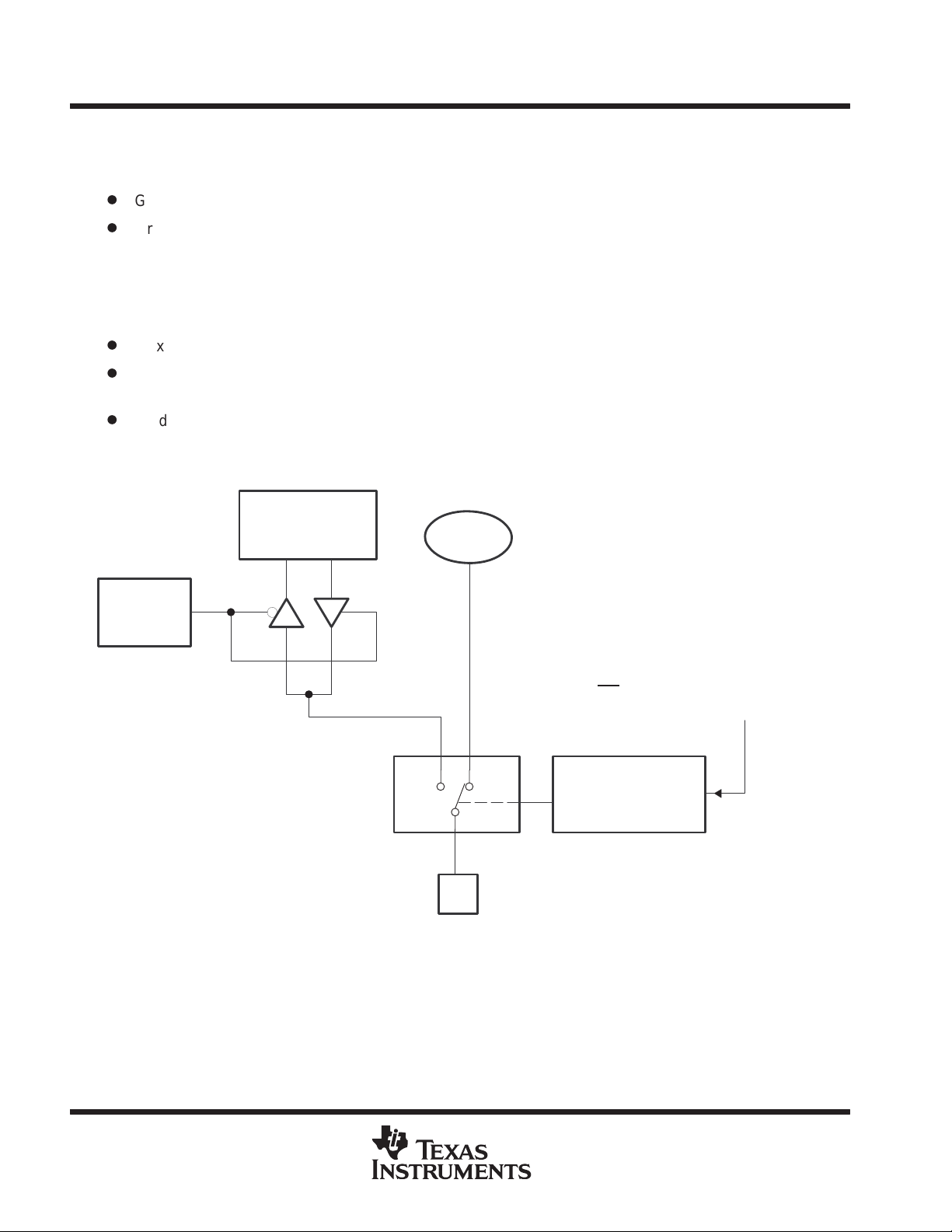
functional block diagram of the TMS320x240 DSP CPU
IS
DS
PS
Control
MUXMUX
ARP(3)
ARB(3)
X1
CLKOUT1
CLKIN/X2
16
PC
W/R
WE
NMI
FLASH EEPROM/
16
1616
MUX
Data/Prog
DARAM
MUX
16
ROM
16
16
AR0(16)
AR1(16)
AR2(16)
AR3(16)
AR4(16)
AR5(16)
AR6(16)
AR7(16)
ARAU(16)
16
16
3
3
3
B0 (256 × 16)
A15–A0
D15–D0
R/W
STRB
READY
MP/MC
XINT[1–3]
16
BR
XF
RS
Data Bus
Memory Map
GREG (16)
3
16
16
3
Register
IMR (16)
IFR (16)
MUX
NPAR
PAR MSTACK
DP(9)
16
MUX
MUX
Data
DARAM
B2 (32 × 16)
B1 (256 × 16)
16
Program Bus
9
9
16
MUX
Stack 8 × 16
16
7
LSB
from
IR
MUX
ISCALE (0–16)
32
16
Program Control
(PCTRL)
16
16
16
16
PSCALE (–6, 0,1,4)
CALU(32)
ACCL(16)ACCH(16)C
OSCALE (0–7)
Data Bus
TREG0(16)
Multiplier
PREG(32)
32
3232
MUX
32
32
32
16
MUX
Data Bus
1616
16
Program Bus
Program Bus
NOTES: A. Symbol descriptions appear in Table 10.
B. For clarity the data and program buses are shown as single buses although they include address and data bits.
30
POST OFFICE BOX 1443 • HOUSTON, TEXAS 77251–1443
Loading...