


 Loading...
TPS23754
TPS23754-1
TPS23756
www.ti.com |
SLVS885B–OCTOBER 2008–REVISED MAY 2009 |
High Power/High Efficiency PoE Interface and DC/DC Controller
FEATURES
∙Powers up to 30 W (input) PDs
∙DC/DC Control Optimized for Isolated Converters
∙Supports High-efficiency Topologies
∙Complete PoE Interface
∙Enhanced Classification per IEEE 802.3at (Draft) with Status Flag
∙Adapter ORing Support
∙Programmable Frequency with Synchronization
∙Robust 100 V, 0.5 Ω Hotswap MOSFET
∙–40°C to 125°C Junction Temperature Range
∙Industry Standard PowerPAD™ TSSOP-20
APPLICATIONS
∙IEEE 802.3at (Draft) Compliant Devices
∙Video and VoIP Telephones
∙RFID Readers
∙Multiband Access Points
∙Security Cameras
DESCRIPTION
The TPS23754/6 is a combined Power over Ethernet (PoE) powered device (PD) interface and current-mode dc/dc controller optimized specifically for isolated converters. The PoE interface supports the IEEE 802.3at (draft) standard.
The TPS23754/6 supports a number of input voltage ORing options including highest voltage, external adapter preference, and PoE preference. These features allow the designer to determine which power source will carry the load under all conditions.
The PoE interface features the new extended hardware classification necessary for compatibility with high-power midspan power sourcing equipment (PSE) per IEEE 802.3at (draft). The detection signature pin can also be used to force power from the PoE source off. Classification can be programmed to any of the defined types with a single resistor.
The dc/dc controller features two complementary gate drivers with programmable dead time. This simplifies design of active-clamp forward converters or optimized gate drive for highly-efficient flyback topologies. The second gate driver may be disabled if desired for single MOSFET topologies. The controller also features internal softstart, bootstrap startup source, current-mode compensation, 78% maximum duty cycle. A programmable and synchronizable oscillator allows design optimization for efficiency and eases use of the controller to upgrade existing power supply designs. Accurate programmable blanking, with a default period, simplifies the usual current-sense filter design trade-offs.
The TPS23754 has a 15 V converter startup while the TPS23756 has a 9 V converter startup. The TPS23754-1 replaces the PPD pin with a no-connect for increased pin spacing.
Pairs 1,2
Pairs 3,4 From Ethernet
From Ethernet
Adapter
|
|
|
|
|
|
|
|
|
|
|
|
|
CIO |
|
|
|
|
|
|
DEN |
|
|
|
|
|
|
|
|
|
|
T1 |
|
|
|
VOUT |
|
|
|
|
|
|
|
|
|
|
|
|
C |
|
|
|
||
|
|
R |
|
|
DD1 |
DD |
|
|
T2P |
|
|
|
IN |
M4 |
LOUT |
RT2P-OUT |
|
|
|
|
|
|
|
|
|
|
|
||||||||
|
|
D |
DEN |
V |
V |
|
|
|
RT2P |
|
|
DVC1 |
|
|
|
||
|
|
1 |
|
|
|
|
|
|
|
|
|
|
|
|
|
|
|
|
|
|
CLS |
|
|
|
|
|
VC |
|
|
|
|
|
|
COUT |
VT2P-OUT |
|
|
CLS |
N/C OR PPD |
|
|
|
|
LVC |
|
DVC2 |
M3 |
|
|||||
|
C |
|
|
|
|
|
|
|
|
||||||||
|
PAD |
|
|
|
|
|
|
|
|
|
|
|
|
||||
|
1 |
|
|
|
|
|
|
|
|
|
|
|
|
|
|
|
|
|
|
R |
|
|
|
|
|
|
|
M1 |
|
|
|
|
|
|
Type 2 PSE |
|
|
|
|
|
|
|
|
VB |
|
|
|
|
|
|
Indicator |
||
|
|
|
V |
|
|
|
|
|
|
C |
|
|
|
|
|
||
|
|
|
SS |
|
|
|
|
|
|
|
|
C |
VB |
|
|
|
|
|
|
|
APD |
|
|
|
|
GATE |
|
M2 |
ROB |
FBU |
|
||||
|
|
|
CTL |
COM ARTN RTN |
|
BLNK |
|
CS |
|
CCTL |
|
||||||
DA |
|
|
FRS |
DT |
GAT2 |
|
|
|
RCTL |
C |
IZ |
R |
|
||||
|
|
|
|
|
|
|
|
|
|
|
|
|
|
|
|||
|
APD2 |
|
FRS |
|
|
|
|
BLNK |
VB |
CCL |
DCL |
|
|
|
|
FBL |
|
RAPD1 |
|
|
|
|
|
VC CS |
|
|
|
|
|
||||||
|
|
R |
|
|
|
|
|
C |
C R |
|
|
|
|
|
|
|
|
|
R |
|
|
|
|
|
R |
|
|
|
TLV431 |
R |
|
||||
Optional |
|
|
|
|
RDT |
|
|
|
|
|
|
|
|
|
|
|
|
Interface |
|
|
|
|
|
|
|
|
|
|
|
|
|
|
|
|
|
Figure 1. High Efficiency Converter Using TPS23754
Please be aware that an important notice concerning availability, standard warranty, and use in critical applications of Texas Instruments semiconductor products and disclaimers thereto appears at the end of this data sheet.
PowerPAD is a trademark of Texas Instruments.
PRODUCTION DATA information is current as of publication date. |
Copyright © 2008–2009, Texas Instruments Incorporated |
Products conform to specifications per the terms of the Texas |
|
Instruments standard warranty. Production processing does not |
|
necessarily include testing of all parameters. |
|

TPS23754
TPS23754-1
TPS23756
SLVS885B–OCTOBER 2008–REVISED MAY 2009 |
www.ti.com |
This device contains circuits to protect its inputs and outputs against damage due to high static voltages or electrostatic fields. These circuits have been qualified to protect this device against electrostatic discharges (ESD) of up to 2 kV according to MIL-STD-883C, Method 3015; however, it is advised that precautions be taken to avoid application of any voltage higher than maximum-rated voltages to these high-impedance circuits. During storage or handling the device leads should be shorted together or the device should be placed in conductive foam. In a circuit, unused inputs should always be connected to an appropriate voltage level, preferably either the proper supply or ground. Specific guidelines for handling devices of this type are contained in the publication Guidelines for Handling Electrostatic-Discharge-Sensitive (ESDS) Devices and Assemblies available from Texas Instruments.
PRODUCT INFORMATION(1)
|
STATUS |
DUTY |
POE UVLO |
CONVERTER UVLO |
FEATURE |
PACKAGE |
MARKING |
|
|
CYCLE |
ON / HYST. |
ON / HYST. |
|
|
|
TPS23754PWP |
Active |
0–78% |
35/4.5 |
15 / 6.5 |
PPD |
TSSOP-20 |
TPS23754 |
|
|
|
|
|
|
PowerPAD™ |
|
TPS23754PWP-1 |
Active |
0–78% |
35/4.5 |
15 / 6.5 |
– |
TSSOP-20 |
23754-1 |
|
|
|
|
|
|
PowerPAD™ |
|
TPS23756PWP |
Active |
0–78% |
35/4.5 |
9 / 3.5 |
PPD |
TSSOP-20 |
TPS23756 |
|
|
|
|
|
|
PowerPAD™ |
|
(1)For the most current package and ordering information, see the Package Option Addendum at the end of this document, or see the TI web site at www.ti.com.
ABSOLUTE MAXIMUM RATINGS(1) (2)
Voltage with respect to VSS unless otherwise noted.
|
VALUE |
UNIT |
Input voltage range, ARTN(2), COM(2), DEN, PPD, RTN(3), VDD, VDD1 |
–0.3 to 100 |
V |
Input voltage range CLS(4) |
-0.3 to 6.5 |
V |
Input voltage range [APD, BLNK(4), CTL, DT(4), FRS(4), VB(4)] to [ARTN, COM] |
–0.3 to 6.5 |
V |
Input voltage range CS to [ARTN,COM] |
–0.3 to VB |
V |
Input voltage range [ARTN, COM] to RTN |
–2 to 2 |
V |
Voltage range VC, T2P, to [ARTN, COM] |
–0.3 to 19 |
V |
Voltage range GATE(4), GAT2(4) to [ARTN, COM] |
–0.3 to VC+0.3 |
V |
Sinking current RTN |
Internally limited |
mA |
Sourcing current VB |
Internally limited |
mA |
Average Sourcing or sinking current, GATE, GAT2 |
25 |
mArms |
ESD rating, HBM |
2 |
kV |
ESD rating, CDM |
500 |
V |
ESD – system level (contact/air) at RJ-45(5) |
8 / 15 |
kV |
Operating junction temperature range, TJ |
–40 to Internally limited |
°C |
(1)Stresses beyond those listed under absolute maximum ratings may cause permanent damage to the device. These are stress ratings only and functional operation of the device at these or any other conditions beyond those indicated under recommended operating conditions is not implied. Exposure to absolute-maximum-rated conditions for extended periods may affect device reliability.
(2)ARTN and COM must be tied to RTN.
(3)IRTN = 0 for VRTN > 80V.
(4)Do not apply voltage to these pins
(5)ESD per EN61000-4-2. A power supply containing the TPS23754 was subjected to the highest test levels in the standard. See the ESD section.
2 |
Submit Documentation Feedback |
Copyright © 2008–2009, Texas Instruments Incorporated |
Product Folder Link(s): TPS23754 TPS23754-1 TPS23756
TPS23754
TPS23754-1
TPS23756
www.ti.com |
SLVS885B–OCTOBER 2008–REVISED MAY 2009 |
RECOMMENDED OPERATING CONDITIONS(1)
Voltage with respect to VSS (unless otherwise noted)
|
MIN |
NOM |
MAX |
UNIT |
Input voltage range ARTN, COM, PPD, RTN, VDD, VDD1 |
0 |
|
57 |
V |
Input voltage range T2P, VC to [ARTN, COM] |
0 |
|
18 |
V |
Input voltage range APD, CTL, DT to [ARTN, COM] |
0 |
|
VB |
V |
Input voltage range CS to [ARTN, COM] |
0 |
|
2 |
V |
Continuous RTN current (T ≤ 125°C)(2) |
|
|
825 |
mA |
J |
|
|
|
|
Sourcing current, VB |
0 |
2.5 |
5 |
mA |
VB capacitance |
0.08 |
|
|
μF |
RBLNK |
0 |
|
350 |
kΩ |
Synchronization pulse width input (when used) |
25 |
|
|
ns |
Operating junction temperature range, TJ |
–40 |
|
125 |
°C |
(1)ARTN and COM tied to RTN.
(2)This is the minimum current-limit value. Viable systems will be designed for maximum currents below this value with reasonable margin. IEEE 802.3at (draft) permits 600mA continuous loading
DISSIPATION RATINGS
PACKAGE |
ΨJT |
θJP |
θJA |
θJA |
MAXIMUM POWER RATING |
|
°C/W(1) |
°C/W |
°C/W(2) |
°C/W(3) |
(W)(4) |
||
|
||||||
PWP (TSSOP-20) |
0.607 |
1.4 |
32.6 |
73.8 |
1.2 |
(1)Thermal resistance junction to case top.
(2)See TI document SLMA002C (or latest version) for recommended layout. This is a best case, natural convection number.
(3)JEDEC method with high-k board (2 signal – 2 plane layers) and power pad not soldered (worst case).
(4)Based on TI recommended layout and 85°C.
ELECTRICAL CHARACTERISTICS
Unless otherwise noted: CS=COM=APD=CTL=RTN=ARTN, GATE & GAT2 float, RFRS=68.1 kΩ, RBLNK=249 kΩ, DT=VB,
PPD=VSS, T2P open, CVB=CVC=0.1 μF, RDEN=24.9 kΩ, RCLS open, 0 V ≤ (VDD, VDD1) ≤ 57 V, 0 V ≤ VC ≤ 18 V, –40°C ≤ TJ ≤ 125°C. Typical specifications are at 25°C.
CONTROLLER SECTION ONLY
[VSS = RTN and VDD=VDD1] or [VSS=RTN=VDD], all voltages referred to [ARTN, COM].
|
PARAMETER |
TEST CONDITIONS |
MIN |
TYP |
MAX |
UNIT |
|
VC |
|
|
|
|
|
|
|
VCUV |
|
VC rising ‘754 |
14.3 |
15 |
15.7 |
|
|
|
VC rising ‘756 |
8.7 |
9 |
9.3 |
|
||
|
UVLO |
V |
|||||
|
Hysteresis ‘754 (1) |
6.2 |
6.5 |
6.8 |
|||
VCUVH |
|
|
|||||
|
Hysteresis ‘756 (1) |
3.3 |
3.5 |
3.7 |
|
||
|
|
|
|||||
|
Operating current |
VC = 12 V, CTL = VB, RDT = 68.1 kΩ |
0.7 |
0.92 |
1.2 |
mA |
|
|
|
‘756, VDD1 = 10.2 V, VC(0) = 0 V |
50 |
85 |
175 |
|
|
tST |
Bootstrap startup time, |
‘756, VDD1 = 35 V, VC(0) = 0 V |
27 |
45 |
92 |
ms |
|
CVC = 22 μF |
‘754, VDD1 = 19.2 V, VC(0) = 0 V |
49 |
81 |
166 |
|||
|
|
||||||
|
|
‘754, VDD1 = 35 V, VC(0) = 0 V |
44 |
75 |
158 |
|
|
|
|
‘754, VDD1 = 19.2 V, VC = 13.9 V |
1.7 |
3.4 |
5.5 |
|
|
|
Startup current source - IVC |
‘756, VDD1 = 10.2 V, VC = 8.6 V |
0.44 |
1.06 |
1.80 |
mA |
|
|
|
‘754, ‘756, VDD1 = 48 V, VC = 0 V |
2.7 |
4.8 |
6.8 |
|
|
VB |
|
|
|
|
|
|
|
|
Voltage |
6.5 V ≤ VC ≤ 18 V, 0 ≤ IVB ≤ 5 mA |
4.8 |
5.10 |
5.25 |
V |
(1)The hysteresis tolerance tracks the rising threshold for a given device.
Copyright © 2008–2009, Texas Instruments Incorporated |
Submit Documentation Feedback |
3 |
Product Folder Link(s): TPS23754 TPS23754-1 TPS23756 |
|
|

TPS23754
TPS23754-1
TPS23756
SLVS885B–OCTOBER 2008–REVISED MAY 2009 |
|
|
|
www.ti.com |
||
|
PARAMETER |
TEST CONDITIONS |
MIN |
TYP |
MAX |
UNIT |
FRS |
|
|
|
|
|
|
|
Switching frequency |
CTL = VB, measure GATE |
|
|
|
kHz |
|
RFRS = 68.1 kΩ |
227 |
253 |
278 |
||
|
|
|
||||
DMAX |
Duty cycle |
CTL= VB, measure GATE |
76 |
78 |
80 |
% |
VSYNC |
Synchronization |
Input threshold |
2 |
2.2 |
2.4 |
V |
CTL |
|
|
|
|
|
|
VZDC |
0% duty cycle threshold |
VCTL ↓ until GATE stops |
1.3 |
1.5 |
1.7 |
V |
|
Softstart period |
Interval from switching start to VCSMAX |
1.9 |
3.9 |
6.2 |
ms |
|
Input resistance |
|
70 |
100 |
145 |
kΩ |
 BLNK
BLNK
|
Blanking delay |
|
|
(In addition to t1) |
|
DT |
|
|
tDT1 |
Dead time |
|
tDT2 |
See Figure 2 for tDTx definition |
|
tDT1 |
|
|
tDT2 |
|
|
CS |
|
|
VCSMAX |
Maximum threshold voltage |
|
t1 |
Turnoff delay |
|
VSLOPE |
Internal slope compensation |
|
voltage |
||
|
||
ISL_EX |
Peak slope compensation |
|
current |
||
|
||
|
Bias current (sourcing) |
|
GATE |
|
|
|
Source current |
|
|
Sink current |
|
GAT2 |
|
|
|
Source current |
Sink current
 APD / PPD
VAPDEN |
APD threshold voltage |
|
VAPDH |
||
|
||
VPPDEN |
|
|
VPPDH |
PPD threshold voltage |
|
VPPD2 |
||
|
||
VPPD2H |
|
|
|
APD leakage current |
|
|
(source or sink) |
|
IPPD |
PPD sink current |
THERMAL SHUTDOWN
Turnoff temperature
Hysteresis(3)
BLNK = RTN |
35 |
55 |
78 |
ns |
|
RBLNK = 49.9 kΩ |
38 |
55 |
70 |
||
|
|||||
CTL = VB, CGATE = 1 nF, |
|
|
|
|
|
CGAT2 = 1 nF, measure GATE, GAT2 |
|
|
|
|
|
RDT = 24.9 kΩ, GAT2 ↑ to GATE ↑ |
40 |
50 |
62.5 |
ns |
|
RDT = 24.9 kΩ, GATE ↓ to GAT2 ↓ |
40 |
50 |
62.5 |
||
|
|||||
RDT = 75 kΩ, GAT2 ↑ to GATE ↑ |
120 |
150 |
188 |
|
|
RDT = 75 kΩ, GATE ↓ to GAT2 ↓ |
120 |
150 |
188 |
|
|
VCTL = VB, VCS rising until GATE duty cycle drops |
0.5 |
0.55 |
0.6 |
V |
|
VCS = 0.65 V |
24 |
40 |
70 |
ns |
|
Peak voltage at maximum duty cycle, referenced to CS |
120 |
155 |
185 |
mV |
|
VCTL = VB, ICS at maximum duty cycle |
30 |
42 |
54 |
μA |
|
DC component of ICS |
1 |
2.5 |
4.3 |
μA |
|
VCTL = VB, VC = 12 V, GATE high, pulsed measurement |
0.37 |
0.6 |
0.95 |
A |
|
VCTL = VB, VC = 12 V, GATE low, pulsed measurement |
0.7 |
1.0 |
1.4 |
A |
|
VCTL = VB, VC = 12 V, GAT2 high, RDT = 24.9 kΩ, pulsed |
0.37 |
0.6 |
0.95 |
A |
|
measurement |
|||||
|
|
|
|
||
VCTL = VB, VC = 12 V, GAT2 low, RDT = 24.9 kΩ, pulsed |
0.7 |
1.0 |
1.4 |
A |
|
measurement |
|||||
|
|
|
|
||
VAPD rising |
1.43 |
1.5 |
1.57 |
V |
|
Hysteresis (2) |
0.29 |
0.31 |
0.33 |
||
|
|||||
VPPD- VVSS rising, UVLO disable |
1.45 |
1.55 |
1.65 |
V |
|
Hysteresis (2) |
0.29 |
0.31 |
0.33 |
||
|
|||||
VPPD- VVSS rising, Class enable |
7.4 |
8.3 |
9.2 |
V |
|
Hysteresis (2) |
0.5 |
0.6 |
0.7 |
||
|
|||||
VC = 12 V, VAPD = VB |
|
|
1 |
μA |
|
VPPD-VSS = 1.5 V |
2.5 |
5 |
7.5 |
μA |
|
TJ rising |
135 |
145 |
155 |
°C |
|
|
|
20 |
|
°C |
(2)The hysteresis tolerance tracks the rising threshold for a given device.
(3)These parameters are provided for reference only, and do not constitute part of TI's published specifications for purposes of TI's product warranty.
4 |
Submit Documentation Feedback |
Copyright © 2008–2009, Texas Instruments Incorporated |
Product Folder Link(s): TPS23754 TPS23754-1 TPS23756

TPS23754
TPS23754-1
TPS23756
www.ti.com |
SLVS885B–OCTOBER 2008–REVISED MAY 2009 |
ELECTRICAL CHARACTERISTICS – PoE AND CONTROL
[VDD=VDD1] or [VDD1=RTN], VC = RTN, COM=RTN=ARTN, all voltages referred to VSS unless otherwise noted
PARAMETER
 DETECTION (DEN)
Detection current
|
Detection bias current |
|
VPD_DIS |
Hotswap disable threshold |
|
|
DEN leakage current |
|
CLASSIFICATION (CLS) |
||
ICLS |
Classification current, |
|
applies to both cycles |
||
|
Classification mark resistance |
|
VCL_ON |
Classification regulator lower |
|
VCL_H |
threshold |
|
VCU_OFF |
Classification regulator upper |
|
VCU_H |
threshold |
|
VMSR |
Mark state reset |
|
|
Leakage current |
|
PASS DEVICE (RTN) |
||
|
On resistance |
|
|
Current limit |
|
|
Inrush limit |
|
|
Foldback voltage threshold |
|
UVLO |
|
|
VUVLO_R |
UVLO threshold |
|
VUVLO_H |
||
|
||
T2P |
|
|
|
ON characteristic |
|
|
Leakage current |
|
tT2P |
Delay |
|
 THERMAL SHUTDOWN
Turnoff temperature Hysteresis(2)
TEST CONDITIONS |
MIN |
TYP |
MAX |
UNIT |
|
(VDD = VDD1 = RTN = VSUPPLY positive) |
|
|
|
|
|
Measure ISUPPLY |
|
|
|
|
|
VDD = 1.6 V |
62 |
64.3 |
66.5 |
μA |
|
VDD = 10 V |
399 |
406 |
414 |
||
|
|||||
VDD = 10 V, float DEN, measure ISUPPLY, |
|
5.6 |
10 |
μA |
|
Note: Not during Mark state |
|
|
|
|
|
|
3 |
4 |
5 |
V |
|
VDEN = VDD = 57 V, float VDD1 and RTN, measure IDEN |
|
0.1 |
5 |
μA |
|
(VDD = VDD1 = RTN = VSUPPLY positive) |
|
|
|
|
|
13 V ≤ VDD ≤ 21 V, Measure ISUPPLY |
|
|
|
|
|
RCLS = 1270 Ω |
1.8 |
2.1 |
2.4 |
|
|
RCLS = 243 Ω |
9.9 |
10.4 |
10.9 |
mA |
|
RCLS = 137 Ω |
17.6 |
18.5 |
19.4 |
||
|
|||||
RCLS = 90.9 Ω |
26.5 |
27.7 |
29.3 |
|
|
RCLS = 63.4 Ω |
38.0 |
39.7 |
42 |
|
|
5.6 V ≤ VDD ≤ 9.4 V |
7.5 |
9.7 |
12 |
kΩ |
|
Regulator turns on, VDD rising |
11.2 |
11.9 |
12.6 |
V |
|
Hysteresis(1) |
1.55 |
1.65 |
1.75 |
||
|
|||||
Regulator turns off, VDD rising |
21 |
22 |
23 |
V |
|
Hysteresis(1) |
0.5 |
0.75 |
1.0 |
||
|
|||||
VDD falling |
3 |
4 |
5 |
V |
|
VDD = 57 V, VCLS = 0 V, DEN = VSS, measure ICLS |
|
|
1 |
μA |
|
(VDD1 = RTN) |
|
|
|
|
|
|
0.25 |
0.43 |
0.75 |
Ω |
|
VRTN = 1.5 V, VDD = 48 V, pulsed measurement |
850 |
970 |
1100 |
mA |
|
VRTN = 2 V, VDD: 0 V → 48 V, pulsed measurement |
100 |
140 |
180 |
mA |
|
VDD rising |
11 |
12.3 |
13.6 |
V |
|
VDD rising |
33.9 |
35 |
36.1 |
V |
|
Hysteresis(1) |
4.4 |
4.55 |
4.76 |
||
|
|||||
Perform classification algorithm, VT2P-RTN = 1 V, |
2 |
|
|
mA |
|
CTL = ARTN |
|
|
|||
|
|
|
|
||
VT2P = 18 V, CTL = VB |
|
|
10 |
μA |
|
From start of switching to T2P active |
5 |
9 |
15 |
ms |
|
TJ rising |
135 |
145 |
155 |
°C |
|
|
|
20 |
|
°C |
(1)The hysteresis tolerance tracks the rising threshold for a given device.
(2)These parameters are provided for reference only, and do not constitute part of TI's published specifications for purposes of TI's product warranty.
Copyright © 2008–2009, Texas Instruments Incorporated |
Submit Documentation Feedback |
5 |
Product Folder Link(s): TPS23754 TPS23754-1 TPS23756
TPS23754
TPS23754-1
TPS23756
SLVS885B–OCTOBER 2008–REVISED MAY 2009 |
www.ti.com |
GATE |
hi |
|
|
|
50% |
||
|
|
||
|
lo |
|
|
GAT2 |
hi |
|
|
|
50% |
||
lo |
time |
||
|
|||
|
tDT1 |
tDT2 |
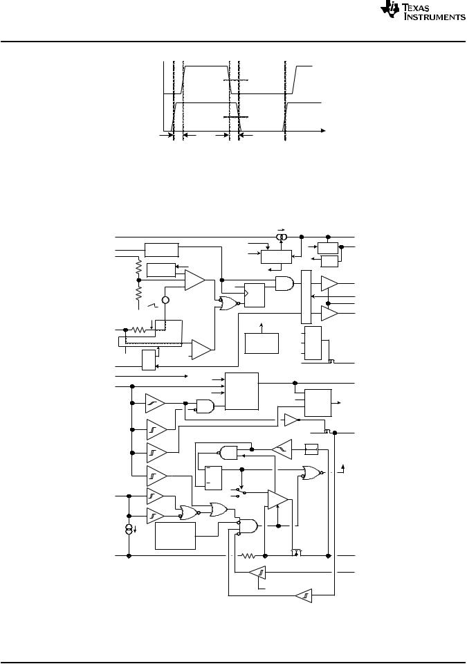
Figure 2. GATE and GAT2 Timing and Phasing
|
|
DEVICE INFORMATION |
|
|
|
|||||
|
FUNCTIONAL BLOCK DIAGRAM |
|
||||||||
VDD1 |
|
|
|
|
φ |
|
|
|
φ |
VC |
|
|
|
|
|
|
|
|
VB |
||
FRS |
Oscillator |
|
|
CONV. |
|
|
|
Reg |
||
CTL |
|
|
|
OFF |
Control |
|
Ref |
|
||
|
|
|
|
|
|
|
|
|
|
|
50kΩ |
4ms |
|
enb |
Global Cvtr. |
enb |
|
|
|
|
|
|
Softstart |
|
- |
Enable |
|
|
|
|
||
|
|
|
|
|
|
|
||||
|
|
|
- |
|
|
|
|
|
|
GATE |
|
|
|
+ |
1 |
D |
Q |
|
|
Deadtime |
|
|
|
|
|
|
|
|||||
50kΩ |
+ |
|
|
|
CK |
|
|
|
|
DT |
|
0.75V |
|
|
|
|
|
|
|
||
|
|
|
CLRB |
|
|
|
COM |
|||
|
|
|
|
|
|
|
|
|||
ARTN |
40µA |
|
|
|
|
|
|
|
|
GAT2 |
(pk) |
|
|
|
|
|
|
|
|
||
|
|
|
|
|
φ |
|
|
|
|
|
3.75kΩ |
|
|
|
|
|
|
|
|
|
|
|
|
|
|
|
|
|
|
|
|
|
CS |
Switch |
|
|
|
|
|
|
t2 |
T2P |
|
|
|
|
|
Converter |
|
|
||||
|
Matrix |
|
+ |
|
|
ss |
|
|||
|
|
|
|
Thermal |
|
Logic |
|
|||
|
|
|
|
|
Monitor |
CTL |
|
|||
|
|
|
|
|
|
|
|
|
||
ARTN |
0.55V |
- |
|
|
|
|
|
|
|
|
|
|
|
|
|
|
|
|
|
||
BLNK |
|
|
|
|
|
|
ARTN |
|
T2P |
|
|
|
|
|
|
|
|
|
|
|
|
ARTN |
|
|
uvlo, φpd |
|
|
2.5V |
|
|
|
|
|
|
|
|
|
|
|
|
CLS |
||
|
|
|
|
Class |
|
|
|
|
||
VDD |
|
|
|
|
|
|
|
|
||
11V & |
pa, sa, den |
Logic & |
|
|
|
|
|
|||
|
|
|
|
T2 |
|
|||||
|
9V |
Regulator |
|
|
|
|
||||
|
|
|
|
uvlo |
|
|||||
|
|
|
|
State |
t2 |
|||||
|
|
|
|
|
|
|
||||
|
|
|
|
|
|
|
|
|
||
|
|
|
|
|
|
|
|
|
Eng. |
|
|
22V & |
|
|
|
|
|
|
|
|
|
|
21.25V |
|
|
|
|
|
|
|
|
|
|
5V |
|
|
|
|
12.5V |
|
VSS |
DEN |
|
|
|
|
|
|
& 1V |
|
|
|
||
|
& 4V |
|
|
|
|
|
|
|
||
|
|
|
|
|
|
|
|
|
|
|
|
|
|
|
|
|
|
|
|
400µs |
CONV. |
|
35V & |
|
|
|
|
|
|
|
OFF |
|
|
|
|
|
|
|
|
|
|
||
|
|
|
|
|
|
|
|
|
|
|
|
30.5V |
|
R |
Q |
|
|
|
|
|
|
|
|
|
|
|
|
|
|
|
||
|
uvlo |
|
|
1 |
|
|
|
|
|
|
|
7.8V |
|
S |
H |
|
ILIM |
|
|
|
|
|
|
|
|
|
|
|
||||
|
|
|
|
|
|
|
|
|
|
|
PPD |
|
|
|
L |
|
+ |
|
|
|
|
|
|
|
0 |
|
|
|
|
|
||
|
1.55V |
|
|
|
- |
|
|
|
|
|
|
|
|
|
|
EN |
|
|
|
||
|
&1.25V |
|
|
|
|
|
|
|
|
|
|
|
|
|
|
|
|
|
|
|
|
|
|
|
pa |
|
|
|
|
|
|
|
|
Common |
|
|
|
|
|
|
|
|
|
|
Circuits and φpd |
|
|
|
|
|
|
|
||
|
PoE Thermal |
|
|
|
|
|
Hotswap |
|
||
|
Monitor |
|
|
|
|
|
MOSFET |
|
||
|
|
|
|
|
|
|
|
|
||
VSS |
|
|
|
|
50mΩ |
|
|
|
|
RTN |
|
|
|
|
|
sa |
1.5V |
|
|
APD |
|
|
|
|
|
|
|
|
|
|||
|
|
|
|
|
|
&1.2V |
|
|
|
|
|
|
|
|
|
den |
ARTN |
|
4V |
|
|
|
|
|
|
|
|
|
|
|
||
6 |
Submit Documentation Feedback |
Copyright © 2008–2009, Texas Instruments Incorporated |
Product Folder Link(s): TPS23754 TPS23754-1 TPS23756
|
|
|
|
|
|
|
TPS23754 |
|
|
|
|
|
|
|
TPS23754-1 |
|
|
|
|
|
|
|
TPS23756 |
www.ti.com |
|
|
|
|
|
SLVS885B–OCTOBER 2008–REVISED MAY 2009 |
|
|
|
|
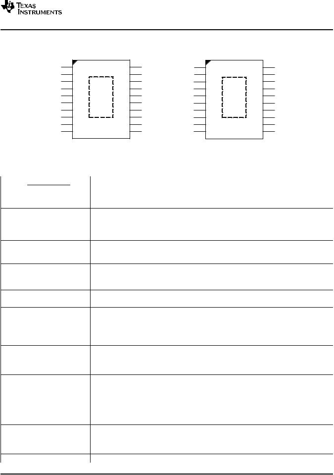
(TOP VIEW) |
|
|
|
|
|
TPS23754/6 |
|
|
TPS23754-1 |
|
||
CTL |
1 |
20 |
T2P |
CTL |
1 |
20 |
T2P |
VB |
2 |
19 |
FRS |
VB |
2 |
19 |
FRS |
|
|||||||
CS |
3 |
18 |
BLNK |
CS |
3 |
18 |
BLNK |
COM |
4 |
17 |
APD |
COM |
4 |
17 |
APD |
GATE |
5 |
16 |
DT |
GATE |
5 |
16 |
DT |
VC |
6 |
15 |
CLS |
VC |
6 |
15 |
CLS |
GAT2 |
7 |
14 |
PPD |
GAT2 |
7 |
14 |
N/C |
ARTN |
8 |
13 |
DEN |
ARTN |
8 |
13 |
DEN |
RTN |
9 |
12 |
VDD |
RTN |
9 |
12 |
VDD |
VSS |
10 |
11 |
VDD1 |
VSS |
10 |
11 |
VDD1 |
PAD = V SS |
PAD = V SS |
|
N/C = Leave Pin Unused |
|
|
|
|
PIN FUNCTIONS |
|
|
NAME |
NO. |
TYPE |
DESCRIPTION |
|
|
|
'754/6 |
‘754-1 |
|
|
|||
|
|
|
|
|
||
CTL |
1 |
1 |
I |
The control loop input to the PWM (pulse width modulator), typically driven by output regulation |
|
|
|
|
|
|
feedback (e.g. optocoupler). Use VB as a pullup for CTL. |
|
|
VB |
2 |
2 |
O |
5.1 V bias rail for dc/dc control circuits and the feedback optocoupler. Typically bypass with a 0.1 μF |
|
|
|
|
|
|
to ARTN. |
|
|
CS |
3 |
3 |
I/O |
DC/DC converter switching MOSFET current sense input. See RCS in Figure 1. |
|
|
COM |
4 |
4 |
|
Gate driver return, connect to ARTN and RTN. |
|
|
GATE |
5 |
5 |
O |
Gate drive output for the main dc/dc converter switching MOSFET. |
|
|
VC |
6 |
6 |
I/O |
DC/DC converter bias voltage. Connect a 0.47 μF (minimum) ceramic capacitor to ARTN at the pin, |
|
|
|
|
|
|
and a larger capacitor to power startup. |
|
|
GAT2 |
7 |
7 |
O |
Gate drive output for a second dc/dc converter switching MOSFET (see Figure 1). |
|
|
ARTN |
8 |
8 |
|
ARTN is the dc/dc converter analog return. Tie to RTN and COM on the circuit board. |
|
|
RTN |
9 |
9 |
|
RTN is the output of the PoE hotswap MOSFET. |
|
|
VSS |
10 |
10 |
|
Connect to the negative power rail derived from the PoE source. |
|
|
VDD1 |
11 |
11 |
I |
Source of dc/dc converter startup current. Connect to VDD for many applications. |
|
|
VDD |
12 |
12 |
I |
Connect to the positive PoE input power rail. VDD powers the PoE interface circuits. Bypass with a |
|
|
|
|
|
|
0.1 μF capacitor and protect with a TVS. |
|
|
DEN |
13 |
13 |
I/O |
Connect a 24.9 kΩ resistor from DEN to VDD to provide the PoE detection signature. Pulling this pin |
|
|
|
|
|
|
to VSS during powered operation causes the internal hotswap MOSFET to turn off. |
|
|
NC |
– |
14 |
|
Float this no-connect pin. |
|
|
PPD |
14 |
– |
I |
Raising VPPD-VSS above 1.55 V enables the hotswap MOSFET and activates T2P. Connecting PPD |
|
|
|
|
|
|
to VDD enables classification when APD is active. Tie PPD to VSS or float when not used. |
|
|
CLS |
15 |
15 |
I |
Connect a resistor from CLS to VSS to program classification current. 2.5 V is applied to the program |
|
|
|
|
|
|
resistor during classification to set class current. |
|
|
DT |
16 |
16 |
I |
Connect a resistor from DT to ARTN to set the GATE to GAT2 dead time. Tie DT to VB to disable |
|
|
|
|
|
|
GAT2 operation. |
|
|
APD |
17 |
17 |
I |
Raising VAPD-VARTN above 1.5 V disables the internal hotswap switch, turns class off, and forces T2P |
||
|
|
|
|
active. This forces power to come from a external VDD1-RTN adapter. Tie APD to ARTN when not |
|
|
|
|
|
|
used. |
|
|
BLNK |
18 |
18 |
I |
Connect to ARTN to utilize the internally set current-sense blanking period, or connect a resistor from |
|
|
|
|
|
|
BLNK to ARTN to program a more accurate period. |
|
|
FRS |
19 |
19 |
I |
Connect a resistor from FRS to ARTN to program the converter switching frequency. FRS may be |
|
|
|
|
|
|
used to synchronize the converter to an external timing source. |
|
|
T2P |
20 |
20 |
O |
Active low output that indicates a PSE has performed the IEEE 802.3at type 2 hardware |
|
|
|
|
|
|
classification, PPD is active, or APD is active. |
|
|
Pad |
– |
– |
|
Connect to VSS. |
|
|
Copyright © 2008–2009, Texas Instruments Incorporated |
Submit Documentation Feedback |
7 |
||||
|
|
|
|
Product Folder Link(s): TPS23754 TPS23754-1 TPS23756 |
|
|

TPS23754
TPS23754-1
TPS23756
SLVS885B–OCTOBER 2008–REVISED MAY 2009 |
www.ti.com |
PIN DESCRIPTION
Refer to Figure 1 for component reference designators (RCS for example), and the Electrical Characteristics table for values denoted by reference (VCSMAX for example). Electrical Characteristic values take precedence over any numerical values used in the following sections.
APD
APD forces power to come from an external adapter connected from VDD1 to RTN by opening the hotswap switch, disabling the CLS output (see PPD pin description), and enabling the T2P output. A resistor divider is recommended on APD when it is connected to an external adapter. The divider provides ESD protection, leakage discharge for the adapter ORing diode, and input voltage qualification. Voltage qualification assures the adapter output voltage is high enough that it can support the PD before the PoE current is cut off.
Select the APD divider resistors per Equation 1 where VADPTR-ON is the desired adapter voltage that enables the APD function as adapter voltage rises.
RAPD1 = RAPD2 × (VADPTR_ON |
− VAPDEN ) VAPDEN |
|||
R APD1 + R APD2 |
× (VAPDEN − VAPDH ) |
|||
VADPTR_OFF = |
|
|
||
R APD2 |
||||
|
(1) |
|||
Place the APD pull-down resistor adjacent to the APD pin.
APD should be tied to ARTN when not used.
BLNK
Blanking provides an interval between GATE going high and the current-control comparators on CS actively monitoring the input. This delay allows the normal turn-on current transient (spike) to subside before the comparators are active, preventing undesired short duty cycles and premature current limiting.
Connect BLNK to ARTN to obtain the internally set blanking period. Connect a resistor from BLNK to ARTN for a more accurate, programmable blanking period. The relationship between the desired blanking period and the programming resistor is defined by Equation 2.
RBLNK (kΩ ) = tBLNK (ns) (2)
Place the resistor adjacent to the BLNK pin when it is used.
CLS
A resistor from CLS to VSS programs the classification current per the IEEE standard. The PD power ranges and corresponding resistor values are listed in Table 1. The power assigned should correspond to the maximum average power drawn by the PD during operation.
High-power PSEs may perform two classification cycles if Class 4 is presented on the first cycle. The TPS23754 presents the same (resistor programmed) class each cycle per the standard.
Table 1. Class Resistor Selection
POWER AT PD |
RESISTOR |
|
||
CLASS MINIMUM |
MAXIMUM |
NOTES |
||
(Ω) |
||||
(W)(W)
0 |
0.44 |
12.95 |
1270 |
Minimum may be reduced by pulsed loading. Serves as a catch-all default class. |
1 |
0.44 |
3.84 |
243 |
|
2 |
3.84 |
6.49 |
137 |
|
3 |
6.49 |
12.95 |
90.9 |
|
4 |
12.95 |
25.5 |
63.4 |
Not allowed for IEEE 802.3-2005. Use to indicate a Type 2 PD (high power) per |
|
|
IEEE 802.3at. |
8 |
Submit Documentation Feedback |
Copyright © 2008–2009, Texas Instruments Incorporated |
|
Product Folder Link(s): TPS23754 TPS23754-1 TPS23756 |
|

TPS23754
TPS23754-1
TPS23756
www.ti.com |
SLVS885B–OCTOBER 2008–REVISED MAY 2009 |
CS
The CS (current sense) input for the dc/dc converter should be connected to the high side of the switching
MOSFET’s current sense resistor (RCS). The current-limit threshold, VCSMAX, defines the voltage on CS above which the GATE ON time will be terminated regardless of the voltage on CTL.
The TPS23754 provides internal slope compensation (150 mV, VSLOPE), an output current for additional slope compensation, a peak current limiter, and an off-time pull-down to this pin.
Routing between the current-sense resistor and the CS pin should be short to minimize cross-talk from noisy traces such as the gate drive signal.
CTL
CTL (control) is the voltage-control loop input to the PWM (pulse width modulator). Pulling VCTL below VZDC causes GATE to stop switching. Increasing VCTL above VZDC (zero duty cycle voltage) raises the switching MOSFET programmed peak current. The maximum (peak) current is requested at approximately VZDC + (2 ×
VCSMAX). The ac gain from CTL to the PWM comparator is 0.5. The internal divider from CTL to ARTN is approximately 100 kΩ.
Use VB as a pull up source for CTL.
DEN
DEN (detection and enable) is a multifunction pin for PoE detection and inhibiting operation from PoE power. Connect a 24.9 kΩ resistor from DEN to VDD to provide the PoE detection signature. DEN goes to a high-impedance state when VVDD-VSS is outside of the detection range. Pulling DEN to VSS during powered operation causes the internal hotswap MOSFET and class regulator to turn off, while the reduced detection resistance prevents the PD from properly re-detecting.
DT
Dead-time programming sets the delay between GATE and GAT2 to prevent overlap of MOSFET ON times as shown in Figure 2. GAT2 turns the second MOSFET off when it transitions high. Both MOSFETs should be off between GAT2 going high to GATE going high, and GATE going low to GAT2 going low. The maximum GATE ON time is reduced by the programmed dead-time period. The dead time period is specified with 1 nF of capacitance on GATE and GAT2. Different loading on these pins will change the effective dead time.
A resistor connected from DT to ARTN sets the delay between GATE and GAT2 per Equation 3.
tDT (ns ) |
|
RDT (kΩ ) = |
(3) |
2 |
|
|
Connect DT to VB to set the dead time to 0 and turn GAT2 off.
FRS
Connect a resistor from FRS (frequency and synchronization) to ARTN to program the converter switching frequency. Select the resistor per the following relationship.
RFRS (kΩ) = |
17250 |
|
|
|
|
||
fSW (kHz) |
|||
|
|||
|
(4) |
||
The converter may be synchronized to a frequency above its maximum free-running frequency by applying short ac-coupled pulses into the FRS pin per Figure 30.
The FRS pin is high impedance. Keep the connections short and apart from potential noise sources. Special care should be taken to avoid crosstalk when synchronizing circuits are used.
GATE
Gate drive output for the dc/dc converter’s main switching MOSFET. GATE’s phase turns the main switch on when it transitions high, and off when it transitions low. GATE is held low when the converter is disabled.
Copyright © 2008–2009, Texas Instruments Incorporated |
Submit Documentation Feedback |
9 |
Product Folder Link(s): TPS23754 TPS23754-1 TPS23756

TPS23754
TPS23754-1
TPS23756
SLVS885B–OCTOBER 2008–REVISED MAY 2009 |
www.ti.com |
GAT2
GAT2 is the second gate drive output for the dc/dc converter. GAT2’s phase turns the second switch off when it transitions high, and on when it transitions low. This drives active-clamp PMOS devices per Figure 1, and driven flyback synchronous rectifiers per Figure 28. See the DT Pin Description for GATE to GAT2 timing. Connecting DT to VB disables GAT2 in a high-impedance condition. GAT2 is low when the converter is disabled.
PPD
PPD is a multifunction pin that has two voltage thresholds, PPD1 and PPD2.
PPD1 permits power to come from an external low voltage adapter, e.g., 24 V, connected from VDD to VSS by
over-riding the normal hotswap UVLO. Voltage on PPD above 1.55 V (VPPDEN) enables the hotswap MOSFET, inhibits class current, and enables T2P. A resistor divider per Figure 35 provides ESD protection, leakage
discharge for the adapter ORing diode, reverse adapter protection, and input voltage qualification. Voltage qualification assures the adapter output voltage is high enough that it can support the PD before it begins to draw current.
|
|
|
|
|
|
|
|
|
|
|
|
|
|
|
|
|
|
|
|
|
|
|
|
V |
|
|
− |
V |
|
|
|
|
|
|
|
|
|
|
|
|
|
|
|
RPPD 1 = |
|
AD PTR _ON |
|
PPDEN |
|
|
|
|
|
|
|
|
|
|
|
|
|
|
|||
|
|
|
VPPD EN |
− |
|
|
|
|
|
|
|
|
|
|
|
|
|
|
|
|
|
|
|
|
|
IPPD |
|
|
|
|
|
|
|
|
|
|
|
|
|
|
|||
|
|
|
RPPD2 |
|
|
|
|
|
|
|
|
|
|
|
|
|
|||||
|
|
|
|
|
|
|
|
|
|
|
|
|
|
|
|
|
|
|
|
|
|
|
|
|
|
|
|
|
|
|
|
(V |
|
− |
V |
) |
|
|
|
|
|||
V |
|
|
= (V |
|
− V |
)+ R |
|
|
PP DEN |
|
PPDH |
|
|
− |
I |
|
|
||||
|
|
|
P PD1 |
|
|
|
|
|
|
|
|||||||||||
ADP TR _OFF |
|
PPD EN |
PPD H |
|
|
|
R |
|
|
|
|
|
PP D |
|
|
||||||
|
|
|
|
|
|
|
|
|
|
|
PPD2 |
|
|
|
|
|
|
||||
|
|
|
|
|
|
|
|
|
|
|
|
|
|
|
|
|
(5) |
||||
|
|
|
|
|
|
|
|
|
|
|
|
|
|
|
|
|
|
|
|
|
|
PPD2 enables normal class regulator operation when VPPD is above 8.3 V to permit type 2 classification when APD is used in conjunction with diode DVDD (see Figure 34). Tie PPD to VDD when PPD2 operation is desired.
The PPD pin has a 5 μA internal pull-down current.
Locate the PPD pull-down resistor adjacent to the pin when used.
PPD may be tied to VSS or left open when not used.
RTN, ARTN, COM
RTN is internally connected to the drain of the PoE hotswap MOSFET, while ARTN is the quiet analog reference for the dc/dc controller return. COM serves as the return path for the gate drivers and should be tied to ARTN on the circuit board. The ARTN / COM / RTN net should be treated as a local reference plane (ground plane) for the dc/dc control and converter primary. RTN and (ARTN/COM) may be separated by several volts for special applications.
T2P
T2P is an active low output that indicates [ (VAPD > 1.5 V) OR (1.55 V ≤ VPPD ≤ 8.3 V) OR (type 2 hardware classification observed) ]. T2P is valid after both a delay of tT2P from the start of converter switching, and [VCTL ≤
(VB – 1 V)]. Once T2P is valid, VCTL will not effect it. T2P will become invalid if the converter goes back into softstart, over-temperature, or is held off by the PD during CIN recharge (inrush). T2P is referenced to ARTN and is intended to drive the diode side of an optocoupler. T2P should be left open or tied to ARTN if not used.
VB
VB is an internal 5.1V regulated dc/dc controller supply rail that is typically bypassed by a 0.1 μF capacitor to ARTN. VB should be used to bias the feedback optocoupler.
VC
VC is the bias supply for the dc/dc controller. The MOSFET gate drivers run directly from VC. VB is regulated down from VC, and is the bias voltage for the rest of the converter control. A startup current source from VDD1 to VC is controlled by a comparator with hysteresis to implement the converter bootstrap startup. VC must be connected to a bias source, such as a converter auxiliary output, during normal operation.
10 |
Submit Documentation Feedback |
Copyright © 2008–2009, Texas Instruments Incorporated |
Product Folder Link(s): TPS23754 TPS23754-1 TPS23756
TPS23754
TPS23754-1
TPS23756
www.ti.com |
SLVS885B–OCTOBER 2008–REVISED MAY 2009 |
A minimum 0.47 μF capacitor, located adjacent to the VC pin, should be connected from VC to COM to bypass the gate driver. A larger total capacitance is required for startup to provide control power between the time the converter starts switching and the availability of the converter auxiliary output voltage.
VDD
VDD is the positive input power rail that is derived from the PoE source (PSE). VDD should be bypassed to VSS with a 0.1 μF capacitor as required by the IEEE standard. A transient suppressor diode (TVS), a special type of Zener diode, such as SMAJ58A should be connected from VDD to VSS to protect against over-voltage transients.
VDD1
VDD1 is the dc/dc converter startup supply. Connect to VDD for many applications. VDD1 may be isolated by a diode from VDD to support PoE priority operation.
VSS
VSS is the PoE input-power return side. It is the reference for the PoE interface circuits, and has a current-limited hotswap switch that connects it to RTN. VSS is clamped to a diode drop above RTN by the hotswap switch.
A local VSS reference plane should be used to connect the input bypass capacitor, TVS, RCLS, and the PowerPad. This plane becomes the main heatsink for the TPS23754.
VSS is internally connected to the PowerPAD.
PowerPAD
The Powerpad is internally connected to VSS. It should be tied to a large VSS copper area on the PCB to provide a low resistance thermal path to the circuit board. It is recommended that a clearance of 0.025” be maintained between VSS, RTN, and various control signals to high-voltage signals such as VDD and VDD1.
TYPICAL CHARACTERISTICS
|
|
DETECTION BIAS CURRENT |
|
|
|
|
|
PoE CURRENT LIMIT |
|
|
||||||
|
|
|
|
vs |
|
|
|
|
|
|
|
vs |
|
|
|
|
|
8 |
|
VOLTAGE |
|
|
|
970 |
|
|
TEMPERATURE |
|
|
|
|||
|
|
|
|
|
|
|
|
|
|
|
|
|
|
|
||
|
7 |
|
|
|
|
|
|
|
Pulsed Current Measurement |
|
|
|
||||
|
|
|
|
|
|
|
960 |
|
|
|
|
|
|
|
|
|
|
|
|
|
|
|
|
|
|
|
|
|
|
|
|
|
|
A |
6 |
|
|
25°C |
|
|
|
|
|
|
|
|
|
|
|
|
|
|
|
|
|
mA |
950 |
|
|
|
|
|
|
|
|
||
5 |
|
|
|
|
|
|
|
|
|
|
|
|
|
|||
− |
|
|
|
|
|
− |
|
|
|
|
|
|
|
|
|
|
− Bias Current |
|
|
|
|
|
Current Limit |
|
|
|
|
|
|
|
|
|
|
4 |
|
125°C |
|
|
|
940 |
|
|
|
|
|
|
|
|
||
3 |
|
|
|
|
|
|
|
|
|
|
|
|
|
|
||
VDD |
|
|
|
|
|
|
− |
930 |
|
|
|
|
|
|
|
|
|
|
|
|
|
|
|
|
|
|
|
|
|
|
|
||
I |
2 |
|
|
|
|
|
PoE |
|
|
|
|
|
|
|
|
|
|
|
|
|
−40 °C |
|
|
|
|
|
|
|
|
|
|
|
|
|
|
|
|
|
|
|
920 |
|
|
|
|
|
|
|
|
|
|
1 |
|
|
|
|
|
|
|
|
|
|
|
|
|
|
|
|
|
|
|
|
|
|
|
|
|
|
|
|
|
|
|
|
|
0 |
|
|
|
|
|
|
910 |
|
|
|
|
|
|
|
|
|
0 |
2 |
4 |
6 |
8 |
10 |
|
−40 |
−20 |
0 |
20 |
40 |
60 |
80 |
100 |
120 |
|
|
(VVDD − V VSS) − PoE V oltage − V |
G001 |
|
|
|
TJ − Junction Temperature − °C |
|
G002 |
|||||||
|
|
|
|
|
|
|
|
|
|
|
|
|
|
|
||
|
|
|
|
Figure 3. |
|
|
|
|
|
|
|
Figure 4. |
|
|
|
|
Copyright © 2008–2009, Texas Instruments Incorporated |
Submit Documentation Feedback |
11 |
Product Folder Link(s): TPS23754 TPS23754-1 TPS23756

TPS23754
TPS23754-1
TPS23756
SLVS885B–OCTOBER 2008–REVISED MAY 2009 |
www.ti.com |
TYPICAL CHARACTERISTICS (continued)
'754 CONVERTER START TIME vs
TEMPERATURE
|
160 |
|
|
|
|
|
|
|
|
|
|
CVC = 22 F |
|
|
|
|
|
|
|
|
140 |
|
|
|
|
|
|
|
|
|
|
|
|
|
VVDD1 = 19.2 V |
|
|
|
|
Time − ms |
120 |
|
|
|
|
|
|
|
|
100 |
|
|
|
|
|
|
|
|
|
Start |
80 |
|
|
|
|
|
|
|
|
Converter |
|
|
|
|
|
|
|
|
|
|
|
|
|
|
VVDD1 = 35 V |
|
|||
60 |
|
|
|
|
|
|
|
|
|
|
|
|
|
|
|
|
|
|
|
|
40 |
|
|
|
|
|
|
|
|
|
20 |
|
|
|
|
|
|
|
|
|
−40 |
−20 |
0 |
20 |
40 |
60 |
80 |
100 |
120 |
|
|
|
TJ − Junction Temperature − °C |
|
|
||||
G003
Figure 5.
'754 CONVERTER STARTUP CURRENT vs
|
6 |
|
|
|
|
VVDD1 |
|
|
|
|
|
|
|
|
VVC = 13.9V |
|
|
|
|
|
|
|
|
||
|
|
|
|
|
|
|
|
TJ = -40oC |
|
|
|
|
|
5 |
|
|
|
|
|
|
|
|
|
|
|
mA |
|
|
|
|
|
|
|
TJ = 25oC |
|
|
|
|
− |
4 |
|
|
|
|
|
|
|
|
|
|
|
SourceCurrent |
3 |
|
|
|
|
|
T = 125oC |
|
|
|
||
|
|
|
|
|
|
|
J |
|
|
|
|
|
|
|
|
|
|
|
|
|
|
|
|
|
|
− |
2 |
|
|
|
|
|
|
|
|
|
|
|
VC |
|
|
|
|
|
|
|
|
|
|
|
|
I |
|
|
|
|
|
|
|
|
|
|
|
|
|
1 |
|
|
|
|
|
|
|
|
|
|
|
|
0 |
|
|
|
|
|
|
|
|
|
|
|
|
5 |
10 |
15 |
20 |
25 |
30 |
35 |
40 |
45 |
50 |
55 |
60 |
|
|
|
|
|
VVDD1-RTN − V |
|
|
|
|
|||
Figure 7.
'756 CONVERTER START TIME vs
TEMPERATURE
|
160 |
|
VVDD1 = 10.2 V |
|
140 |
|
CVC = 22 F |
|
120 |
ms |
100 |
Time− |
80 |
Start |
|
|
60 |
|
40 |
|
VVDD1 = 35 V |
20 |
|
|
|
|
|
|
|
|
−40 |
−20 |
0 |
20 |
40 |
60 |
80 |
100 |
120 |
TJ - Junction Temperature - oC
Figure 6.
'756 CONVERTER STARTUP CURRENT vs
|
|
|
|
|
|
VVDD1 |
|
|
|
|
|
|
|
6 |
|
|
|
|
|
|
|
|
|
|
|
|
|
VVC = 8.6V |
|
|
|
|
|
|
|
|
||
|
|
|
|
|
|
|
|
TJ = -40oC |
|
|
|
|
|
5 |
|
|
|
|
|
|
|
|
|
|
|
mA |
|
|
|
|
|
|
|
TJ = 25oC |
|
|
|
|
− |
4 |
|
|
|
|
|
|
|
|
|
|
|
SourceCurrent |
3 |
|
|
|
|
|
TJ = 125oC |
|
|
|
||
|
|
|
|
|
|
|
|
|
|
|
|
|
− |
2 |
|
|
|
|
|
|
|
|
|
|
|
VC |
|
|
|
|
|
|
|
|
|
|
|
|
I |
|
|
|
|
|
|
|
|
|
|
|
|
|
1 |
|
|
|
|
|
|
|
|
|
|
|
|
0 |
|
|
|
|
|
|
|
|
|
|
|
|
5 |
10 |
15 |
20 |
25 |
30 |
35 |
40 |
45 |
50 |
55 |
60 |
|
|
|
|
|
VVDD1-RTN − V |
|
|
|
|
|||
Figure 8.
12 |
Submit Documentation Feedback |
Copyright © 2008–2009, Texas Instruments Incorporated |
Product Folder Link(s): TPS23754 TPS23754-1 TPS23756

TPS23754
TPS23754-1
TPS23756
www.ti.com |
SLVS885B–OCTOBER 2008–REVISED MAY 2009 |
TYPICAL CHARACTERISTICS (continued)
|
|
|
CONTROLLER BIAS CURRENT |
|
|
||||
|
|
|
|
|
vs |
|
|
|
|
|
|
|
|
TEMPERATURE |
|
|
|||
|
3000 |
|
|
|
|
|
|
|
|
|
|
GATE and GAT2 Open |
|
|
|
|
|||
|
|
VVC = 12 V |
|
|
|
|
|
|
|
|
2500 |
|
|
|
|
|
|
|
|
− A |
2000 |
|
|
|
|
|
|
|
|
|
|
484 kHz |
|
|
937 kHz |
|
|
||
|
|
|
|
|
|
|
|||
− Sinking |
1500 |
|
|
|
|
|
|
|
|
|
|
|
100 kHz |
|
245 kHz |
|
|
||
VC |
|
|
|
|
|
|
|
||
1000 |
|
|
|
|
|
|
|
|
|
I |
|
|
|
|
|
|
|
|
|
|
|
|
|
|
|
|
|
|
|
|
500 |
|
|
|
|
|
|
|
|
|
|
|
|
|
50 kHz |
|
VCTL = 0 V |
|
|
|
0 |
|
|
|
|
|
|
|
|
|
−40 |
−20 |
0 |
20 |
40 |
60 |
80 |
100 |
120 |
|
|
|
TJ - Junction Temperature - °C |
|
|
||||
'754 CONTROLLER BIAS CURRENT vs
VOLTAGE
|
3500 |
|
|
|
|
|
|
|
|
|
|
|
GATE and GAT2 Open |
|
|
|
|
|
|||
|
3000 |
TJ = 25°C |
|
|
|
|
|
|
|
|
|
|
|
|
|
|
|
|
|
|
|
A |
|
|
937 kHz |
|
|
|
|
|
|
|
− |
2500 |
|
|
|
|
|
|
|
|
|
Current |
|
|
|
|
|
|
|
|
|
|
|
|
|
|
|
|
484 kHz |
|
|
||
2000 |
|
|
|
|
|
|
|
|
|
|
ControllerBias |
|
|
|
|
245 kHz |
|
|
|
|
|
1500 |
|
100 kHz |
|
|
|
|
|
|
|
|
|
|
|
|
|
|
|
|
|
||
1000 |
|
|
|
|
|
|
|
|
|
|
− |
|
|
|
|
|
|
|
|
|
|
|
|
|
|
|
|
|
|
|
|
|
C |
|
|
|
|
|
|
|
|
|
|
I |
|
|
|
|
|
|
|
|
|
|
|
500 |
|
|
|
|
|
|
|
|
|
|
|
|
|
50 kHz |
|
|
VCTL = 0 V |
|
||
|
0 |
|
|
|
|
|
|
|
|
|
|
9 |
10 |
11 |
12 |
13 |
14 |
15 |
16 |
17 |
18 |
G005 |
|
|
VC − Controller Bias Voltage − V |
|
G006 |
|||||
|
|
|
|
|
|
|
|
|
||
Figure 9. |
Figure 10. |
'756 CONTROLLER BIAS CURRENT vs
VOLTAGE
|
4000 |
GATE, GAT2 open |
|
|
|
|
|
|
|
|
|
|
|
||
|
3500 |
TJ = 25oC |
|
|
|
|
|
|
|
|
|
|
|
|
|
|
|
|
|
|
960 kHz |
|
|
− A |
3000 |
|
|
|
|
|
|
2500 |
|
|
|
|
|
|
|
− BiasCurrent |
|
|
|
|
|
|
|
|
|
|
|
480 kHz |
|
||
2000 |
|
|
|
|
|
|
|
1500 |
|
100 kHz |
|
|
|
|
|
|
|
|
|
|
|
||
C |
|
50 kHz |
|
|
250 kHz |
|
|
V |
|
|
|
|
|
|
|
|
1000 |
|
|
|
|
|
|
|
500 |
|
|
|
|
|
|
|
0 |
|
|
|
VCTL = 0 V |
|
|
|
|
|
|
|
|
|
|
|
6 |
8 |
10 |
12 |
14 |
16 |
18 |
|
|
VC − Controller Bias Voltage − V |
|
|
|||
|
|
|
|
SWITCHING FREQUENCY |
|
|
|
||||
|
|
|
|
|
|
vs |
|
|
|
|
|
|
|
|
|
|
TEMPERATURE |
|
|
|
|
||
|
600 |
|
|
|
|
|
|
|
|
1200 |
|
|
|
RFRS = 34.6 kΩ (484 kHz) |
|
|
|
|
|
|
|||
|
500 |
|
|
|
|
|
|
|
|
1100 |
|
−kHz |
400 |
RFRS = 17.35 kΩ (937 kHz) |
|
|
|
|
1000 |
−kHz |
|||
SwitchingFrequency |
300 |
RFRS = 69.8 kΩ (245 kHz) |
|
|
|
|
900 |
SwitchingFrequency |
|||
200 |
|
|
|
RFRS = 347 kΩ (50 kHz) |
800 |
||||||
|
RFRS = 173 kΩ (100 kHz) |
|
|
|
|
|
|||||
|
100 |
|
|
|
|
|
|
|
|
700 |
|
|
0 |
|
|
|
|
|
|
|
|
600 |
|
|
−40 |
−20 |
0 |
20 |
40 |
60 |
80 |
100 |
120 |
|
|
|
|
|
TJ - Junction Temperature - °C |
|
|
|
G007 |
||||
|
|
|
|
|
|
|
|
|
|
|
|
Figure 11. |
Figure 12. |
Copyright © 2008–2009, Texas Instruments Incorporated |
Submit Documentation Feedback |
13 |
Product Folder Link(s): TPS23754 TPS23754-1 TPS23756
Loading...