


TPS5633EVM-104
Texas Instruments TPS5633EVM-104, TPS5633EVM-111, TPS5625PWPR, TPS5625PWP, TPS5625EVM-105 Datasheet
...
TPS5615, TPS5618, TPS5625, TPS5633
SYNCHRONOUS-BUCK HYSTERETIC REGULATOR CONTROLLER
SLVS177A – SEPTEMBER 1998 – REVISED NOVEMBER 1998
1
POST OFFICE BOX 655303 • DALLAS, TEXAS 75265
D
±1% Reference Over Full Operating
T emperature Range
D
Synchronous Rectifier Driver for >90%
Efficiency
D
Fixed Output Voltage Options of 1.5 V,
1.8 V, 2.5 V, and 3.3 V
D
User-Selectable Hysteretic-T ype Control
D
Low Supply Current...3 mA Typ
D
11.4-V to 13-V Input Voltage Range, V
CC
D
Power Good Output
D
Programmable Soft-Start
D
Overvoltage/Overcurrent Protection
D
Active Deadtime Control
description
The TPS5615 family of synchronous-buck regulator controllers provides an accurate supply voltage to DSPs.
The output voltage is internally set by a resistive divider with an accuracy of 1% over the full operating
temperature range. A hysteretic controller with user-selectable hysteresis is used to dramatically reduce
overshoot and undershoot caused by load transients. Propagation delay from the comparator inputs to the
output drivers is less than 250 ns. Overcurrent shutdown and crossover protection for the output drivers
combine to eliminate destructive faults in the output FETs. PWRGD monitors the output voltage and pulls the
open-collector output low when the output drops below 93% of the nominal output voltage. An overvoltage circuit
disables the output drivers if the output voltage rises 15% above the nominal value. The inhibit pin can be used
to control power sequencing. Inhibit and undervoltage lockout assures that the 12-V supply voltage and system
supply voltage (5 V or 3.3 V) are within proper operating limits before the controller starts. The output driver
circuits include 2-A drivers with internal 8-V gate-voltage regulators that can easily provide sufficient power for
today’s high-powered DSPs. The high-side driver can be configured either as a ground-referenced driver or as
a floating bootstrap driver. The TPS5615 family is available in a 28-pin TSSOP PowerPad package. It operates
over a junction temperature range of 0°C to 125°C.
AVAILABLE OPTIONS
PACKAGE
T
J
OUTPUT VOLTAGE
TSSOP
†
(PWP)
1.5 V TPS5615PWP
°
°
1.8 V TPS5618PWP
0°C
to
125°C
2.5 V TPS5625PWP
3.3 V TPS5633PWP
†
The PWP package is availble taped and reeled. Add R suffix to
device type (e.g., TPS5615PWPR).
Copyright 1998, Texas Instruments Incorporated
PRODUCTION DATA information is current as of publication date.
Products conform to specifications per the terms of Texas Instruments
standard warranty. Production processing does not necessarily include
testing of all parameters.
Please be aware that an important notice concerning availability, standard warranty, and use in critical applications of
Texas Instruments semiconductor products and disclaimers thereto appears at the end of this data sheet.
1
2
3
4
5
6
7
8
9
10
11
12
13
14
28
27
26
25
24
23
22
21
20
19
18
17
16
15
IOUT
AGND2
OCP
VHYST
VREFB
VSENSE
ANAGND
SLOWST
BIAS
LODRV
LOHIB
DRVGND
LOWDR
DRV
PWRGD
NC
NC
NC
NC
NC
INHIBIT
IOUTLO
LOSENSE
HISENSE
BOOTLO
HIGHDR
BOOT
V
CC
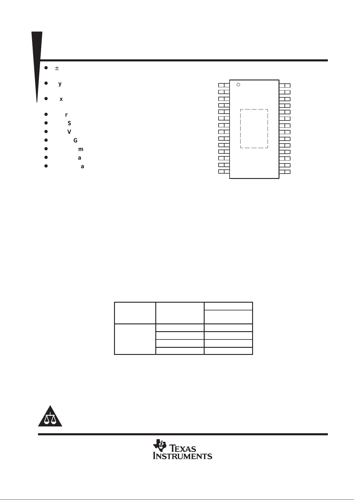
PWP PACKAGE
(TOP VIEW)
NC – No internal connection
PowerPAD is a trademark of Texas Instruments Incorporated.
TPS5615, TPS5618, TPS5625, TPS5633
SYNCHRONOUS-BUCK HYSTERETIC REGULATOR CONTROLLER
SLVS177A – SEPTEMBER 1998 – REVISED NOVEMBER 1998
2
POST OFFICE BOX 655303 • DALLAS, TEXAS 75265
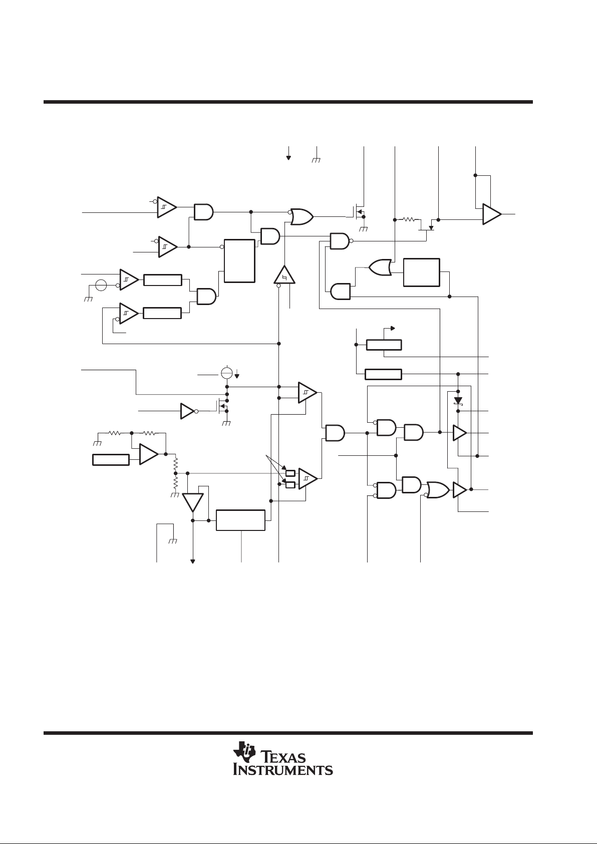
functional block diagram
INHIBIT
OCP
SLOWST
IOUT
BIAS
DRV
BOOT
HIGHDR
BOOTLO
LOWDR
DRVGND
HISENSEIOUTLOLOSENSEPWRGDANAGND
CC
V
VREFBAGND2 VSENSEVHYST LODRVLOHIB
_
+
2 V
10 V
UVLO
V
CC
22
3
8
25 4 6 11 10
15 7 28 20
21
19
1
9
14
16
17
18
13
12
_
+
Deglitch
100mV
VOVP
1.15 VREF
VSENSE
S
R
Q
V
CC
Deglitch
Fault
Shutdown
VPGD
0.93 VREF
Rising
Edge
Delay
HIGHIN
HIGHDR
2X
Shutdown
_
+
Bandgap
_
+
I
VREFB
5
Analog
Bias
VREF
Hysteresis
Setting
I
VREFB
_
+
_
+
Hysteresis
Comparator
Shutdown
Slowstart
Comparator
CM Filters
PREREG
DRV REG
V
CC
Analog
Bias
TPS5615, TPS5618, TPS5625, TPS5633
SYNCHRONOUS-BUCK HYSTERETIC REGULATOR CONTROLLER
SLVS177A – SEPTEMBER 1998 – REVISED NOVEMBER 1998
3
POST OFFICE BOX 655303 • DALLAS, TEXAS 75265
Terminal Functions
TERMINAL
NAME NO.
I/O
DESCRIPTION
AGND2 2 Analog ground (must be connected).
ANAGND 7 Analog ground
BIAS 9 Analog bias pin. A 1-µF capacitor should be connected from BIAS to ANAGND.
BOOT 16 Bootstrap. A 1-µF capacitor should be connected from BOOT to BOOTLO.
BOOTLO 18 Bootstrap low. Connect to the junction of the high-side and low-side FETs for floating drive configuration.
Connect to PGND for ground-reference drive configuration.
DRV 14 Drive regulator for the FET drivers. A 1-µF capacitor should be connected from DRV to DRVGND.
DRVGND 12 Drive ground. Ground for FET drivers. Connect to FET PWRGND.
HIGHDR 17 High drive. Output drive to high-side power switching FETs.
HISENSE 19 High current sense. For current sensing across high-side FET s, connect to the drain of the high-side FETs;
for optional current sensing scheme, connect to power supply side of current-sense resistor placed in series
with high-side FET drain.
INHIBIT 22 Disables the drive signals to the MOSFET drivers. Also serves as UVLO for system logic supply (3.3 V or
5 V). An external pull-up resistor should be connected to system-logic supply.
IOUT 1 Current out. Output voltage on this terminal is proportional to the load current as measured across the
R
ds(on)
of the high side FET . The voltage on this terminal equals 2 ×R
DS(ON)
×IOUT . In applications where
very accurate current-sensing is required, a sense resistor should be connected between the input supply
and the drain of the high-side FETs.
IOUTLO 21 Current sense low output. This is the voltage on the LOSENSE terminal when the high-side FETs are on.
A ceramic capacitor (between 0.033 µF and 0.1 µF) should be connected from IOUTLO to HISENSE to hold
the sensed voltage.
LODRV 10 Low drive enable. Normally tied to 5 V. To configure the low-side FET as a crowbar , pull LODRV low.
LOHIB 11 Low side inhibit. Connect to the junction of the high- and low-side FETs to control the anti-cross-
conduction and eliminate shoot-through current. Disabled when configured in crowbar mode.
LOSENSE 20 Low current sense. For current sensing across high-side FET s, connect to the source of the high-side FET s;
for optional current sensing scheme, connect to high-side FET drain side of current-sense resistor placed
in series with high-side FET drain.
LOWDR 13 Low drive. Output drive to synchronous rectifier FETs.
NC 23–27 No connect
OCP 3 Over current protection. Current limit trip point is set with a resistor divider between IOUT and ANAGND.
PWRGD 28 Power good. PWRGD signal goes high when output voltage is within 7% of voltage setpoint. Open-drain
output.
SLOWST 8 Slow Start (soft start). A capacitor form SLOWST to ANAGND sets the slowstart time.
Slowstart current = I
VREFB
/5
VHYST 4 Hysteresis set input. The hysteresis is set with a resistor divider from VREFB to ANAGND.
Hysteresis = 2 × (VREFB – VHYST)
V
CC
15 12-V supply. A 1-µF capacitor should be connected from V
CC
to DRVGND.
VREFB 5 Buffered reference voltage
VSENSE 6 Voltage sense Input. T o be connected from converter output voltage bus to sense and control output voltage.
It is recommended that a RC low-pass filter be connected at this pin to filter noise.
TPS5615, TPS5618, TPS5625, TPS5633
SYNCHRONOUS-BUCK HYSTERETIC REGULATOR CONTROLLER
SLVS177A – SEPTEMBER 1998 – REVISED NOVEMBER 1998
4
POST OFFICE BOX 655303 • DALLAS, TEXAS 75265
detailed description
Vref
The reference voltage section consists of a temperature-compensated bandgap reference and a resistive
divider that sets the output voltage option. The output voltage, VREF, is within 1% of the nominal setting over
the full junction temperature range of 0°C to 125°C, and a V
CC
supply voltage range of 11.4 V to 12.6 V. The
output of the reference network is indirectly brought out through a buffer to the VREFB pin. The voltage on this
pin will be within 2% of VREF . It is not recommended to drive loads with VREFB, other than setting the hysteresis
of the hysteretic comparator, because the current drawn from VREFB sets the charging current for the slowstart
capacitor. Refer to the
slowstart
section for additional information.
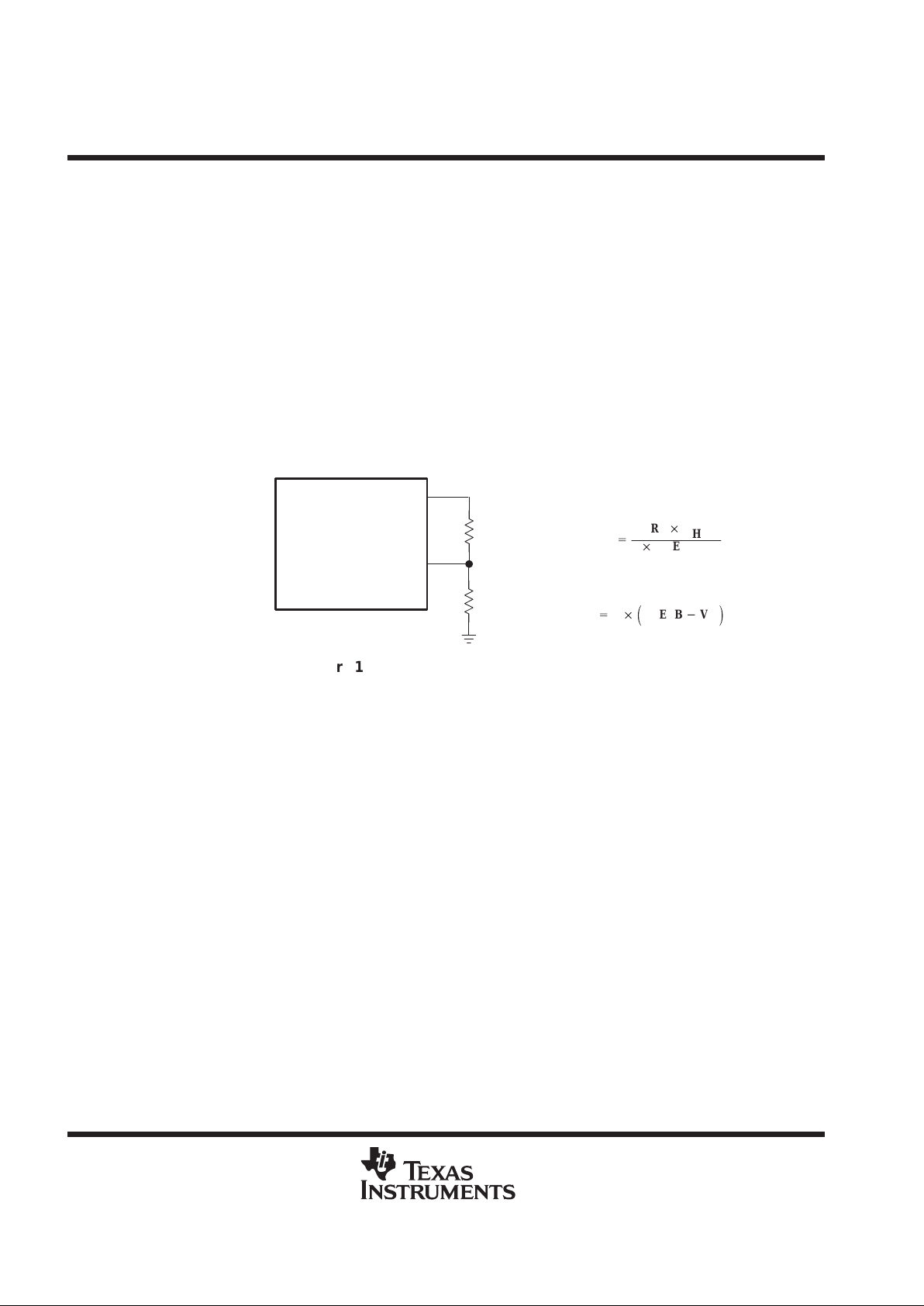
hysteretic comparator
The hysteretic comparator regulates the output voltage of the synchronous-buck converter. The hysteresis is
set by 2 external resistors and is centered on VREF . The 2 external resistors form a resistor divider from VREFB
to ANAGND, with the output voltage connecting to the VHYST pin. The hysteresis of the propagation delay from
the comparator inputs to the driver outputs is 250 ns (maximum). The maximum hysteresis setting is 60 mV.
R1
+
R2
V
H
2
VREFB–V
H
Where
V
H
=
desired
hysteresis
voltage
I
O(MAX)
= 0.5 µA
VHYST
TPS56xx
VREFB
R1
R2
+
2
ǒ
VREFB
*
V
H
Ǔ
Figure 1. Setting the Hysteresis Voltage
low-side driver
The low-side driver is designed to drive low-R
ds(on)
n-channel MOSFETs. The current rating of the driver is 2
A, source or sink. The bias to the low-side driver is internally connected to the DRV regulator.
high-side driver
The high-side driver is designed to drive low-R
ds(on)
n-channel MOSFETs. The current rating of the driver is 2
A, source or sink. The high-side driver can be configured either as a ground-referenced driver or as a floating
bootstrap driver. When configured as a floating driver , the bias voltage to the driver is developed from the DR V
regulator. The internal bootstrap diode, connected between the DR V and BOOT pins, is a Schottky for improved
drive efficiency. The maximum voltage that can be applied between BOOT and DRVGND is 30 V. The driver
can be referenced to ground by connecting BOOTLO to DRVGND, and connecting BOOT to either DRV or V
CC
.
deadtime control
Deadtime control prevents shoot-through current from flowing through the main power FETs during switching
transitions by actively controlling the turn-on times of the MOSFET drivers. The high-side driver is not allowed
to turn on until the gate-drive voltage to the low-side FET is below 2 V; the low-side driver is not allowed to turn
on until the voltage at the junction of the 2 FETs (Vphase) is below 2 V.
TPS5615, TPS5618, TPS5625, TPS5633
SYNCHRONOUS-BUCK HYSTERETIC REGULATOR CONTROLLER
SLVS177A – SEPTEMBER 1998 – REVISED NOVEMBER 1998
5
POST OFFICE BOX 655303 • DALLAS, TEXAS 75265
detailed description (continued)
current sensing
Current sensing is achieved by sampling and holding the voltage across the high-side power FET while the
high-side FET is on. The sampling network consists of an internal 60-Ω switch and an external ceramic hold
capacitor. Recommended value of the hold capacitor is between 0.033 µ F and 0.1 µF. The actual value should
give a time constant (60 Ω × C
H
) greater than the FET on time. Internal logic controls the turn-on and turn-off
of the sample/hold switch such that the switch does not turn on until the Vphase voltage transitions high, and
the switch turns off when the input to the high-side driver goes low . Thus sampling will occur only when the high
side FET is conducting current. The voltage on the IOUT pin equals 2 times the sensed high-side voltage. In
applications where a higher accuracy in current-sensing is required, a sense resistor can be placed in series
with the high-side FET and the voltage across the sense resistor can be sampled by the current sensing circuit.
See Figures 2 and 3.
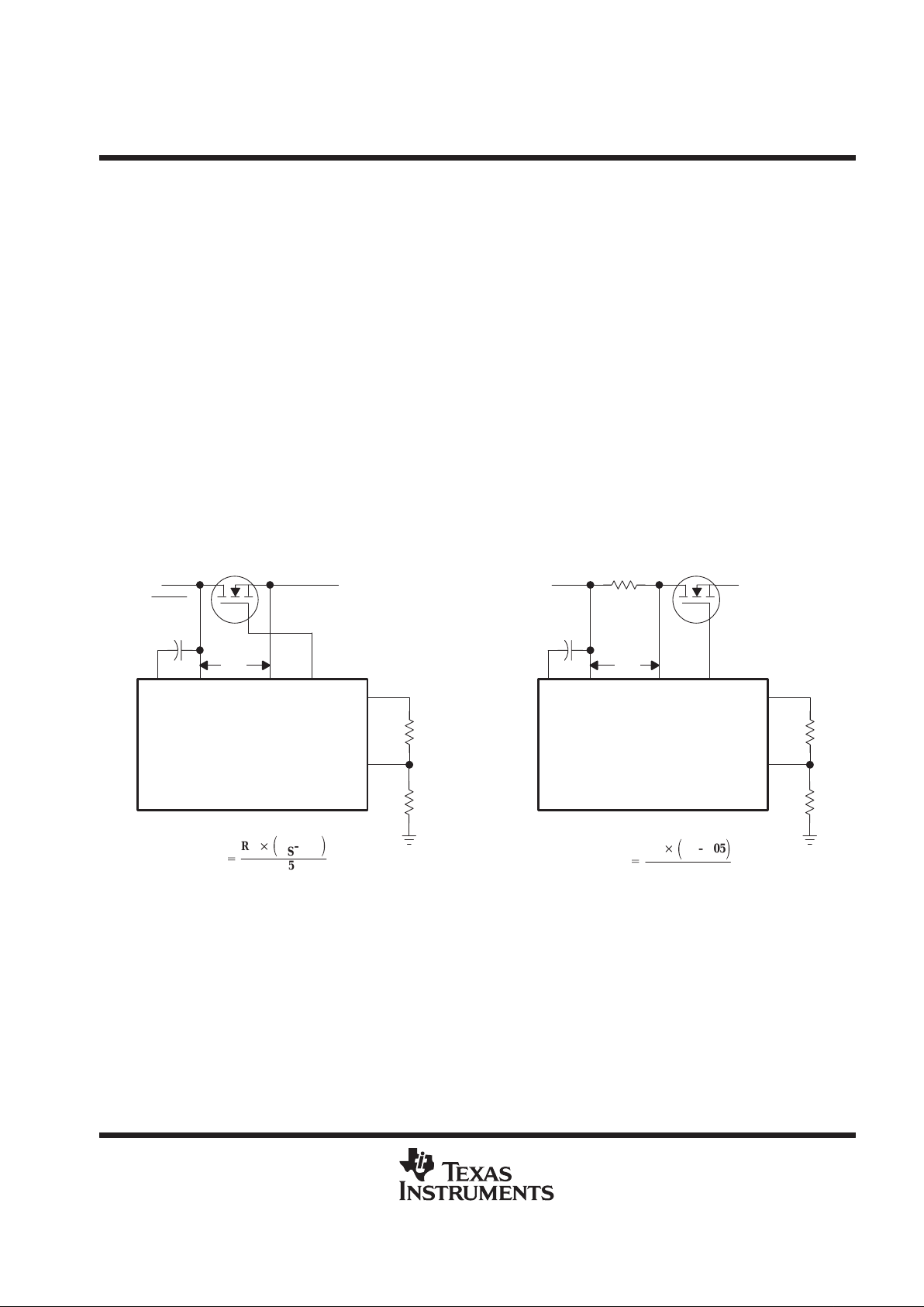
overcurrent protection
The overcurrent protection (OCP) circuit monitors the current through the high-side FET. The overcurrent
threshold is adjustable with an external resistor divider between IOUT and ANAGND, with the divider voltage
connected to OCP. If the voltage on OCP (V
S
) exceeds 100 mV , then a fault latch is set and the output drivers
are turned off. The latch will remain set until V
CC
goes below the undervoltage lockout value. A 3-µs deglitch
timer is included for noise immunity . The OCP circuit is also designed to protect the high-side power FET against
a short-to-ground fault on the terminal common to both power FETs (Vphase).
R1
+
R2
ǒ
V
S
–0.05
Ǔ
0.05
Figure 2. OCP Using FET ON-Resistance
Figure 3. Precision OCP Using External Resistor
R1
+
R2
ǒ
V
S
–0.05
Ǔ
0.05
R2
2 * V
S
OCP
TPS56xx
R1
IOUT
IOUTLO
HISENSE
LOSENSE
HIGHDR
V
CC
V
P
C
H
V
S
R2
2 * V
S
OCP
TPS56xx
R1
IOUT
IOUTLO
HISENSE
LOSENSE
HIGHDR
V
CC
V
P
C
H
V
S
R
S
inhibit
INHIBIT is a TTL-compatible digital input used to enable the controller. When INHIBIT is low , the output drivers
are low and the slowstart capacitor is discharged. When INHIBIT goes high, the short across the slowstart
capacitor is released and normal converter operation begins. When the system-logic supply is connected to
INHIBIT, it also controls power sequencing by locking out controller operation until the system-logic supply
exceeds the input threshold voltage of the inhibit circuit. Thus the 12-V supply and the system-logic supply
(either 5 V or 3.3 V) must be above UVLO thresholds before the controller is allowed to start up. The INHIBIT
comparator start threshold is 2.1 V and the hysteresis is 100 mV.
TPS5615, TPS5618, TPS5625, TPS5633
SYNCHRONOUS-BUCK HYSTERETIC REGULATOR CONTROLLER
SLVS177A – SEPTEMBER 1998 – REVISED NOVEMBER 1998
6
POST OFFICE BOX 655303 • DALLAS, TEXAS 75265
detailed description (continued)
R2
+
2.1
R1
V
TRIP
–2.1
Where
V
TRIP
=desired V
SUPPLY
trip voltage
R2
INHIBIT
TPS56xx
R1
To Power Stage
SHUTDOWN
V
CC
Figure 4. Input Undervoltage Lockout Circuit Using INHIBIT
V
CC
undervoltage lockout (UVLO)
The undervoltage lockout circuit disables the controller while the V
CC
supply is below the 10-V start threshold
during power-up. While the controller is disabled, the output drivers will be low and the slowstart capacitor will
be shorted. When V
CC
exceeds the start threshold, the short across the slowstart capacitor is released and
normal converter operation begins. There is a 2-V hysteresis in the undervoltage lockout circuit for noise
immunity.
slowstart
The slowstart circuit controls the rate at which V
O
powers up. A capacitor is connected between SLOWSST and
ANAGND and is charged by an internal current source. The slowstart charging current is determined by the
following equation:
I
SLOWSTART
+
I(VREFB)
5
where I(VREFB) is the current flowing out of VREFB. It is recommended that no additional loads be connected
to VREFB, other than the resistor divider for setting the hysteresis voltage. The maximum current that can be
sourced by the VREFB circuit is 500 µA. The slowstart time is set by:
t
SLOWSTART
+
5
C
SLOWST
R
VREFB
where R
VREFB
is the total external resistance from VREFB to ANAGND.
power good
The power good circuit monitors for an undervoltage condition on V
O
. If V
O
is 7% below V
REF
, then PWRGD
is pulled low. PWRGD is an open-drain output.
overvoltage protection
The overvoltage protection (OVP) circuit monitors V
O
for an overvoltage condition. If V
O
is 15% above V
REF
,
then a fault latch is set and both output drivers are turned off. The latch will remain set until V
CC
goes below the
undervoltage lockout value. A 3-µs deglitch timer is included for noise immunity. Refer to the LODRV section
for information on how to protect the load against overvoltages due to a shorted fault across the high-side power
FET .
TPS5615, TPS5618, TPS5625, TPS5633
SYNCHRONOUS-BUCK HYSTERETIC REGULATOR CONTROLLER
SLVS177A – SEPTEMBER 1998 – REVISED NOVEMBER 1998
7
POST OFFICE BOX 655303 • DALLAS, TEXAS 75265
detailed description (continued)
drive regulator
The drive regulator provides drive voltage to the output drivers. The minimum drive voltage is 7 V . The minimum
short circuit current is 100 mA. Connect a 1-µF ceramic capacitor from DRV to DRVGND.
LODRV
The LODRV circuit is designed to protect the load against overvoltages that occur if the high-side FET s become
shorted. External components to sense an overvoltage condition are required to use this feature. When an
overvoltage fault occurs, LODRV is pulled low and the low-side FET will be turned on, overriding all control
signals inside the TPS56xx controller. The crowbar action will short the system-logic supply to ground through
the faulted high-side FET s and the low-side FETs. A fuse, in series with V
IN
, should be added to disconnect the
short circuit.
absolute maximum ratings over operating free-air temperature (unless otherwise noted)
†
Supply voltage range, V
CC
(see Note 1) –0.3 to 14 V. . . . . . . . . . . . . . . . . . . . . . . . . . . . . . . . . . . . . . . . . . . . . . .
Input voltage range: BOOT to DRVGND (high-side driver ON) –0.3 to 30 V. . . . . . . . . . . . . . . . . . . . . . . . . . .
BOOT to HIGHDRV –0.3 to 15 V. . . . . . . . . . . . . . . . . . . . . . . . . . . . . . . . . . . . . . . . . . . . . .
BOOT to BOOTLO –0.3 to 15 V. . . . . . . . . . . . . . . . . . . . . . . . . . . . . . . . . . . . . . . . . . . . . . .
INHIBIT, LODRV –0.3 to 7.3 V. . . . . . . . . . . . . . . . . . . . . . . . . . . . . . . . . . . . . . . . . . . . . . . . .
PWRGD, OCP –0.3 to 7 V. . . . . . . . . . . . . . . . . . . . . . . . . . . . . . . . . . . . . . . . . . . . . . . . . . .
LOHIB, LOSENSE, IOUTLO, HISENSE –0.3 to 14 V. . . . . . . . . . . . . . . . . . . . . . . . . . . .
VSENSE –0.3 to 5 V. . . . . . . . . . . . . . . . . . . . . . . . . . . . . . . . . . . . . . . . . . . . . . . . . . . . . . . .
Voltage difference between ANAGND and DRVGND ±0.5 V. . . . . . . . . . . . . . . . . . . . . . . . . . . . . . . . . . . . . . . . .
Output current, VREFB 0.5 mA. . . . . . . . . . . . . . . . . . . . . . . . . . . . . . . . . . . . . . . . . . . . . . . . . . . . . . . . . . . . . . . . . . .
Short circuit duration, DRV Continuous. . . . . . . . . . . . . . . . . . . . . . . . . . . . . . . . . . . . . . . . . . . . . . . . . . . . . . . . . . . .
Continuous total power dissipation See Dissipation Rating Table. . . . . . . . . . . . . . . . . . . . . . . . . . . . . . . . . . . . .
Operating junction temperature range, T
J
0°C to 125°C. . . . . . . . . . . . . . . . . . . . . . . . . . . . . . . . . . . . . . . . . . . . .
Storage temperature range, T
stg
–65°C to 150°C. . . . . . . . . . . . . . . . . . . . . . . . . . . . . . . . . . . . . . . . . . . . . . . . . . .
Lead temperature soldering 1,6 mm (1/16 inch) from case for 10 seconds 260°C. . . . . . . . . . . . . . . . . . . . . . .
†
Stresses beyond those listed under “absolute maximum ratings” may cause permanent damage to the device. These are stress ratings only, and
functional operation of the device at these or any other conditions beyond those indicated under “recommended operating conditions” is not
implied. Exposure to absolute-maximum-rated conditions for extended periods may affect device reliability.
NOTE 1: Unless otherwise specified, all voltages are with respect to ANAGND.
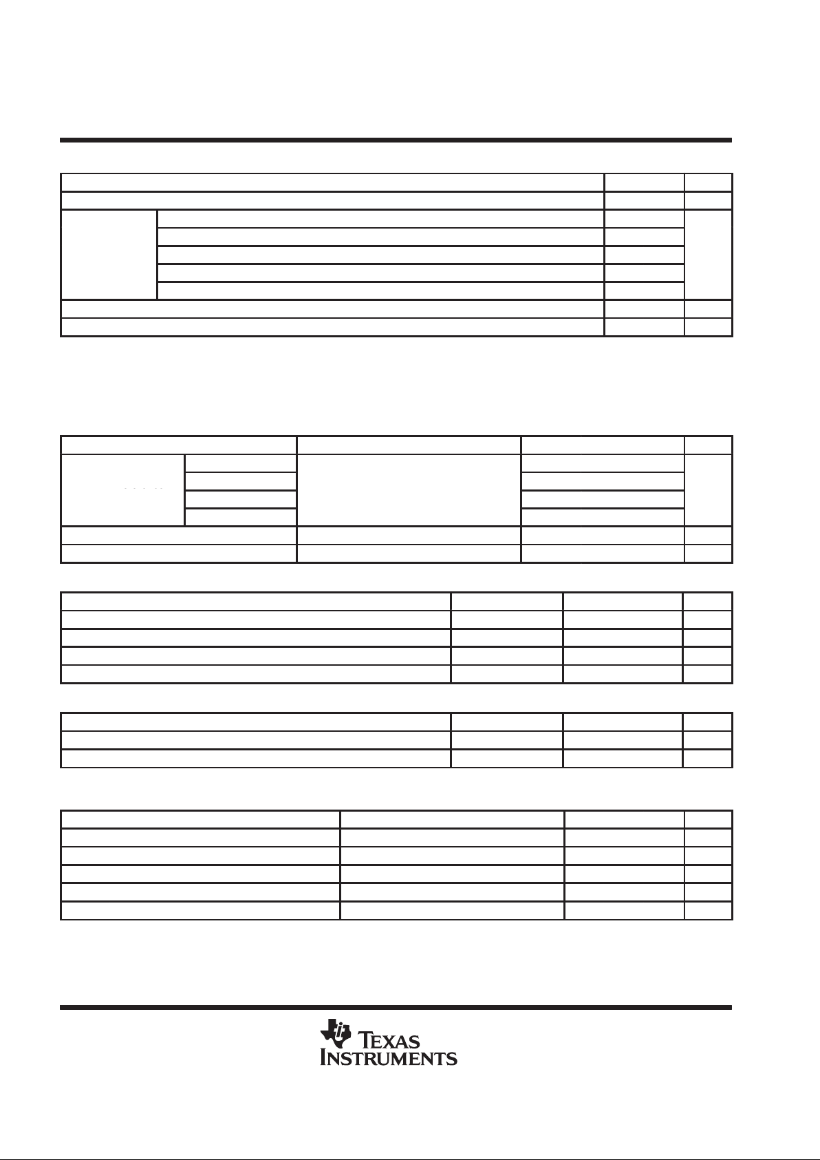
DISSIPATION RATING TABLE
PACKAGE
T
A
≤ 25°C
POWER RATING
DERATING FACTOR
ABOVE T
A
= 25°C
T
A
= 70°C
POWER RATING
T
A
= 85°C
POWER RATING
PWP 1150 mW 11.5 mW/°C 630 mW 460 mW
TPS5615, TPS5618, TPS5625, TPS5633
SYNCHRONOUS-BUCK HYSTERETIC REGULATOR CONTROLLER
SLVS177A – SEPTEMBER 1998 – REVISED NOVEMBER 1998
8
POST OFFICE BOX 655303 • DALLAS, TEXAS 75265
recommended operating conditions
MIN MAX UNIT
Supply voltage, V
CC
11.4 13 V
BOOT to DRVGND 0 28
BOOT to BOOTLO 0 13
Input voltage
INHIBIT, LODRV, PWRGD, OCP 0 6
V
LOHIB, LOSENSE, IOUTLO, HISENSE 0 13
VSENSE 0 4.5
Voltage dif ference between ANAGND and DRVGND 0 ±0.2 V
Output current, VREFB
†
0 0.4 mA
†
Not recommended to load VREFB other than to set hysteresis since I
VREFB
sets slowstart time.
electrical characteristics over recommended operating virtual junction temperature range,
V
CC
= 12 V, I
DRV
= 0 A (unless otherwise noted)
reference
PARAMETER TEST CONDITIONS MIN TYP MAX UNIT
TPS5615 1.485 1.515
Reference
TPS5618
1.782 1.818
VREF
Reference
voltage
TPS5625
V
CC
=
11
.
4
V
to
12
.
6
V
2.475 2.525
V
TPS5633 3.267 3.333
VREFB Output voltage I
REFB
= 50 µA VREF–2% VREF VREF+2% V
VREFB Output regulation 10 µA ≤ I
O
≤ 500 µA 2 mV
power good
PARAMETER TEST CONDITIONS MIN TYP MAX UNIT
Undervoltage trip threshold 90 93 95 %VREF
Low-level output voltage, PWRGD I
O
= 5 mA 0.5 0.75 V
High-level input current, PWRGD V
PWRGD
= 6 V 1 µA
Hysteresis 10 mV
overvoltage protection
PARAMETER TEST CONDITIONS MIN TYP MAX UNIT
Overvoltage trip threshold 112 115 120 %VREF
Hysteresis See Note 2 10 mV
NOTE 2: Ensured by design, not tested.
slowstart
PARAMETER TEST CONDITIONS MIN TYP MAX UNIT
Charge current V
SLOWST
= 0.5 V, I
VREFB
= 65 µA 10.4 13 15.6 µA
Discharge current V
SOFTST
= 1 V 3 mA
Comparator input offset voltage 10 mV
Comparator input bias current See Note 2 10 100 nA
Hysteresis –7.5 7.5 mV
NOTE 2: Ensured by design, not tested.
 Loading...