


Texas Instruments TMX320C6201BGJL, TMS320C6201GGP200, TMS320C6201GGP167, TMS320C6201GJLA200, TMS320C6201GJL200 Datasheet
...TMS320C6201, TMS320C6201B DIGITAL SIGNAL PROCESSORS
SPRS051F ± JANUARY 1997 ± REVISED AUGUST 1999
DHighest Performance Fixed-Point Digital Signal Processor (DSP) TMS320C6201
±6-, 5-ns Instruction Cycle Time
±167-, 200-MHz Clock Rate
±Eight 32-Bit Instructions/Cycle
±1336, 1600 MIPS
DHighest Performance Fixed-Point Digital Signal Processor (DSP) TMS320C6201B
±5-, 4.3-ns Instruction Cycle Time
±200-, and 233-MHz Clock Rates
±Eight 32-Bit Instructions/Cycle
±1600, 1860 MIPS
DVelociTI Advanced Very Long Instruction
Word (VLIW) 'C62x CPU Core
±Eight Independent Functional Units:
±Six ALUs (32-/40-Bit)
±Two 16-Bit Multipliers (32-Bit Results)
±Load-Store Architecture With 32 32-Bit General-Purpose Registers
±Instruction Packing Reduces Code Size
±All Instructions Conditional
DInstruction Set Features
±Byte-Addressable (8-, 16-, 32-Bit Data)
±32-Bit Address Range
±8-Bit Overflow Protection
±Saturation
±Bit-Field Extract, Set, Clear
±Bit-Counting
±Normalization
D1M-Bit On-Chip SRAM
±512K-Bit Internal Program/Cache
(16K 32-Bit Instructions)
±512K-Bit Dual-Access Internal Data
(64K Bytes) Organized as a Single Block ('6201)
±512K-Bit Dual-Access Internal Data
(64K Bytes) Organized as Two Blocks for Improved Concurrency ('6201B)
D32-Bit External Memory Interface (EMIF)
±Glueless Interface to Synchronous Memories: SDRAM and SBSRAM
±Glueless Interface to Asynchronous Memories: SRAM and EPROM
DFour-Channel Bootloading Direct-Memory-Access (DMA) Controller with an Auxiliary Channel
GJC/GJL/GGP
352-PIN BALL GRID ARRAY (BGA) PACKAGES
(BOTTOM VIEW)
AF
AE
AD
AC
AB
AA
Y
W
V
U
T
R
P
N
M
L
K
J
H
G
F
E
D
C
B
A
1 |
3 |
5 |
7 |
9 |
11 |
13 |
15 |
17 |
19 |
21 |
23 |
25 |
|
2 |
4 |
6 |
8 |
10 |
|
12 |
14 |
16 |
18 |
20 |
22 |
24 |
26 |
D16-Bit Host-Port Interface (HPI)
±Access to Entire Memory Map
DTwo Multichannel Buffered Serial Ports (McBSPs)
±Direct Interface to T1/E1, MVIP, SCSA Framers
±ST-Bus-Switching Compatible
±Up to 256 Channels Each
±AC97-Compatible
±Serial Peripheral Interface (SPI) Compatible (Motorola )
DTwo 32-Bit General-Purpose Timers
DFlexible Phase-Locked Loop (PLL) Clock Generator
DIEEE-1149.1 (JTAG²) Boundary-Scan Compatible
D352-Pin BGA Package (GGP Suffix) ('6201)
D352-Pin BGA Package (GJC Suffix) ('6201B)
D352-Pin BGA Package (GJL Suffix) ('6201B)
DCMOS Technology
±0.25- m/5-Level Metal Process ('6201)
±0.18- m/5-Level Metal Process ('6201B)
D3.3-V I/Os, 2.5-V Internal ('6201)
D3.3-V I/Os, 1.8-V Internal ('6201B)
Please be aware that an important notice concerning availability, standard warranty, and use in critical applications of Texas Instruments semiconductor products and disclaimers thereto appears at the end of this data sheet.
VelociTI is a trademark of Texas Instruments Incorporated. Motorola is a trademark of Motorola, Inc.
² IEEE Standard 1149.1-1990 Standard-Test-Access Port and Boundary Scan Architecture.
UNLESS OTHERWISE NOTED this document contains PRODUCTION |
Copyright 1999, Texas Instruments Incorporated |
DATA information current as of publication date. Products conform to |
|
specifications per the terms of Texas Instruments standard warranty. |
|
Production processing does not necessarily include testing of all |
|
parameters. |
|
POST OFFICE BOX 1443 •HOUSTON, TEXAS 77251±1443 |
1 |

TMS320C6201, TMS320C6201B
DIGITAL SIGNAL PROCESSORS
SPRS051F ± JANUARY 1997 ± REVISED AUGUST 1999
description
The TMS320C62x² DSPs (including the TMS320C6201 and the TMS320C6201B devices) are the fixed-point DSP family in the TMS320C6000 platform. The TMS320C6201 ('C6201) and the TMS320C6201B ('C6201B) devices are based on the high-performance, advanced VelociTI very-long-instruction-word (VLIW) architecture developed by Texas Instruments (TI ), making these DSPs an excellent choice for multichannel and multifunction applications. With performance of up to 1600 million instructions per second (MIPS) at a clock rate of 200 MHz, the 'C6201 offers cost-effective solutions to high-performance DSP programming challenges. The 'C6201B is a newer revision of the 'C6201 with performance of up to 1860 MIPS at a clock rate of 233 MHz. The 'C6201/'C6201B DSPs possess the operational flexibility of high-speed controllers and the numerical capability of array processors. Each of these processors have 32 general-purpose registers of 32-bit word length and eight highly independent functional units. The eight functional units provide six arithmetic logic units (ALUs) for a high degree of parallelism and two 16-bit multipliers for a 32-bit result. Both the 'C6201 and the 'C6201B can produce two multiply-accumulates (MACs) per cycleÐfor a total of 400 million MACs per second (MMACS) for the 'C6201, and a total of 466 MMACS for the 'C6201B. The 'C62x DSP also has application-specific hardware logic, on-chip memory, and additional on-chip peripherals.
The 'C6201/'C6201B includes a large bank of on-chip memory and has a powerful and diverse set of peripherals. Program memory consists of a 64K-byte block that is user-configurable as cache or memory-mapped program space. Data memory of the 'C6201 consists of a 64K-byte block of RAM, while data memory of the 'C6201B consists of two 32K-byte blocks of RAM for improved concurrency. The peripheral set includes two multichannel buffered serial ports (McBSPs), two general-purpose timers, a host-port interface (HPI), and a glueless external memory interface (EMIF) capable of interfacing to SDRAM or SBSRAM and asynchronous peripherals.
The 'C62x has a complete set of development tools which includes: a new C compiler, an assembly optimizer to simplify programming and scheduling, and a Windows debugger interface for visibility into source code execution.
device characteristics
Table 1 provides an overview of the 'C62x DSP. The table shows significant features of each device, including the capacity of on-chip RAM, the peripherals, the execution time, and the package type with pin count.
Table 1. Characteristics of the 'C6201/'C6201B Processors
CHARACTERISTICS |
|
DESCRIPTION |
||
|
|
|
|
|
Device Number |
TMS320C6201 |
|
TMS320C6201B |
|
|
|
|
|
|
On-Chip Memory |
512-Kbit Program Memory |
|
512-Kbit Program Memory |
|
512-Kbit Data Memory (organized as a single block) |
512-Kbit Data Memory (organized as two blocks) |
|||
|
||||
|
|
|
|
|
|
2 Multichannel Buffered Serial Ports (McBSPs) |
|
2 Multichannel Buffered Serial Ports (McBSPs) |
|
Peripherals |
2 General-Purpose Timers |
|
2 General-Purpose Timers |
|
Host-Port Interface (HPI) |
|
Host-Port Interface (HPI) |
||
|
|
|||
|
External Memory Interface (EMIF) |
|
External Memory Interface (EMIF) |
|
|
|
|
|
|
Cycle Time |
5 ns (TMS320C6201-200), |
|
4.3 ns (TMS320C6201B-233), |
|
6 ns (TMS320C6201-167) |
|
5 ns (TMS320C6201B-200) |
||
|
|
|||
|
|
|
|
|
Package Type |
35 mm × 35 mm, 352-Pin BGA (GGP) |
|
35 mm × 35 mm, 352-Pin BGA (GJC), |
|
|
27 mm × 27 mm, 352-Pin BGA (GJL) |
|||
|
|
|
||
|
|
|
|
|
Nominal Voltage |
2.5 V Core |
|
1.8 V Core |
|
3.3 V I/O |
|
3.3 V I/O |
||
|
|
|||
|
|
|
|
|
TI is a trademark of Texas Instruments Incorporated.
Windows is a registered trademark of the Microsoft Corporation.
²Where unique device characteristics are specified, TMS320C6201 and TMS320C6201B identifiers are used. For generic characteristics, no identifiers are needed, 'C62x is used, or 'C6000 is used.
2 |
POST OFFICE BOX 1443 •HOUSTON, TEXAS 77251±1443 |
TMS320C6201, TMS320C6201B
DIGITAL SIGNAL PROCESSORS
SPRS051F ± JANUARY 1997 ± REVISED AUGUST 1999
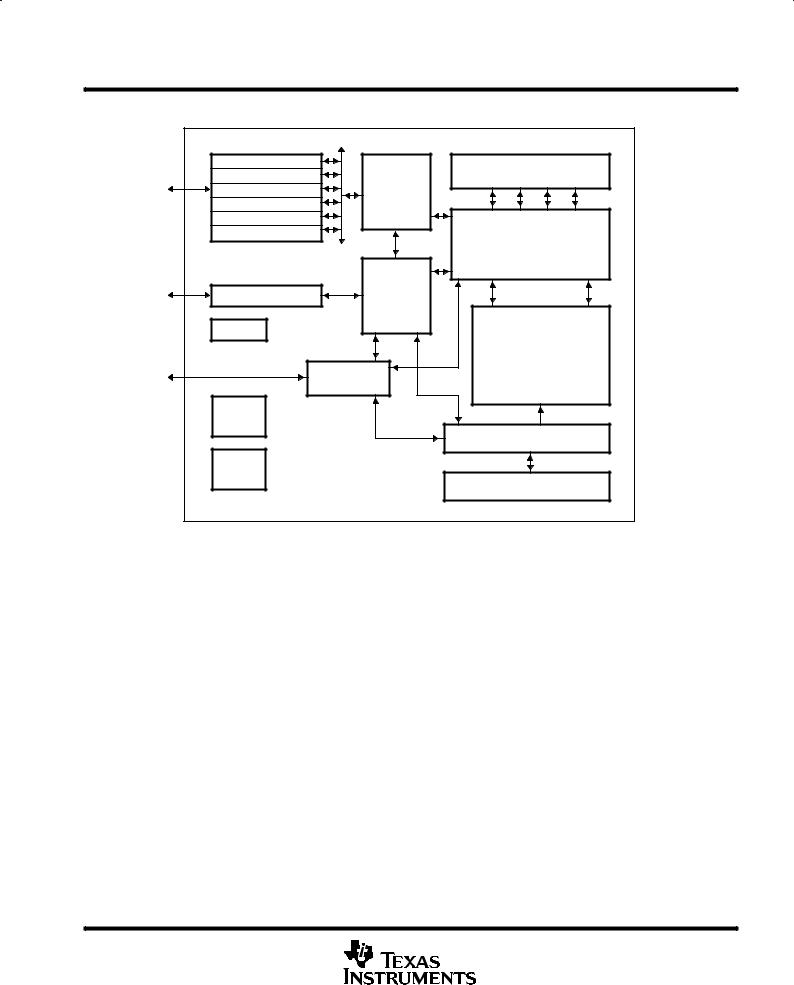
functional block diagram
Timers |
Data Memory |
|
Interrupt Selector |
||
Peripheral |
||
McBSPs |
||
Bus |
||
HPI Control |
Controller |
|
DMA Control |
|
|
EMIF Control |
Data Memory |
|
|
||
|
Controller |
|
Host-Port Interface |
DMA |
|
Controller |
||
|
||
PLL |
|
|
|
CPU |
|
|
EMIF |
|
Power |
|
|
Down |
|
|
|
Program Memory Controller |
|
Boot- |
|
|
Config. |
Program Memory/Cache |
|
|
POST OFFICE BOX 1443 •HOUSTON, TEXAS 77251±1443 |
3 |

TMS320C6201, TMS320C6201B
DIGITAL SIGNAL PROCESSORS
SPRS051F ± JANUARY 1997 ± REVISED AUGUST 1999
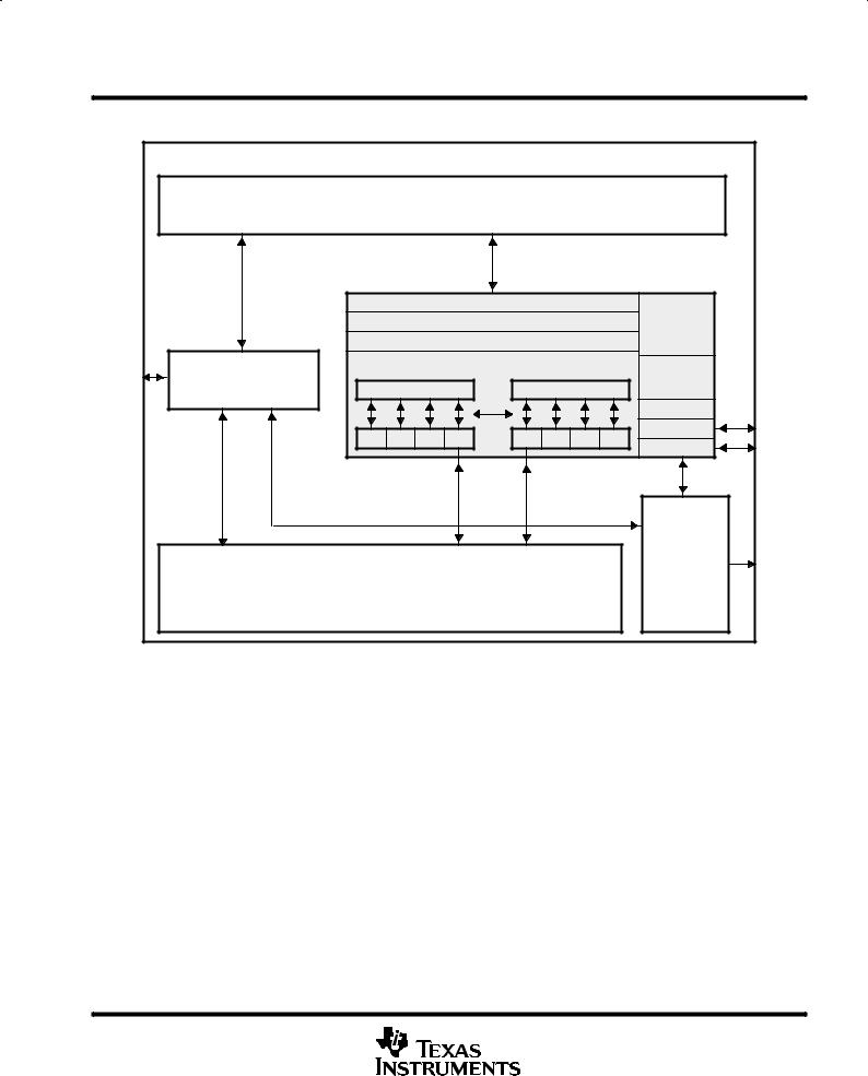
CPU description
The CPU fetches VelociTI advanced very-long instruction words (VLIW) (256 bits wide) to supply up to eight 32-bit instructions to the eight functional units during every clock cycle. The VelociTI VLIW architecture features controls by which all eight units do not have to be supplied with instructions if they are not ready to execute. The first bit of every 32-bit instruction determines if the next instruction belongs to the same execute packet as the previous instruction, or whether it should be executed in the following clock as a part of the next execute packet. Fetch packets are always 256 bits wide; however, the execute packets can vary in size. The variable-length execute packets are a key memory-saving feature, distinguishing the 'C62x CPU from other VLIW architectures.
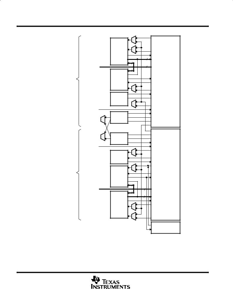
The CPU features two sets of functional units. Each set contains four units and a register file. One set contains functional units .L1, .S1, .M1, and .D1; the other set contains units .D2, .M2, .S2, and .L2. The two register files each contain 16 32-bit registers for a total of 32 general-purpose registers. The two sets of functional units, along with two register files, compose sides A and B of the CPU (see Figure 1 and Figure 2). The four functional units on each side of the CPU can freely share the 16 registers belonging to that side. Additionally, each side features a single data bus connected to all the registers on the other side, by which the two sets of functional units can access data from the register files on the opposite side. While register access by functional units on the same side of the CPU as the register file can service all the units in a single clock cycle, register access using the register file across the CPU supports one read and one write per cycle.
Another key feature of the 'C62x CPU is the load/store architecture, where all instructions operate on registers (as opposed to data in memory). Two sets of data-addressing units (.D1 and .D2) are responsible for all data transfers between the register files and the memory. The data address driven by the .D units allows data addresses generated from one register file to be used to load or store data to or from the other register file. The 'C62x CPU supports a variety of indirect addressing modes using either linearor circular-addressing modes with 5- or 15-bit offsets. All instructions are conditional, and most can access any one of the 32 registers. Some registers, however, are singled out to support specific addressing or to hold the condition for conditional instructions (if the condition is not automatically ªtrueº). The two .M functional units are dedicated for multiplies. The two .S and .L functional units perform a general set of arithmetic, logical, and branch functions with results available every clock cycle.
The processing flow begins when a 256-bit-wide instruction fetch packet is fetched from a program memory. The 32-bit instructions destined for the individual functional units are ªlinkedº together by ª1º bits in the least significant bit (LSB) position of the instructions. The instructions that are ªchainedº together for simultaneous execution (up to eight in total) compose an execute packet. A ª0º in the LSB of an instruction breaks the chain, effectively placing the instructions that follow it in the next execute packet. If an execute packet crosses the fetch packet boundary (256 bits wide), the assembler places it in the next fetch packet, while the remainder of the current fetch packet is padded with NOP instructions. The number of execute packets within a fetch packet can vary from one to eight. Execute packets are dispatched to their respective functional units at the rate of one per clock cycle and the next 256-bit fetch packet is not fetched until all the execute packets from the current fetch packet have been dispatched. After decoding, the instructions simultaneously drive all active functional units for a maximum execution rate of eight instructions every clock cycle. While most results are stored in 32-bit registers, they can be subsequently moved to memory as bytes or half-words as well. All load and store instructions are byte-, half-word, or word-addressable.
4 |
POST OFFICE BOX 1443 •HOUSTON, TEXAS 77251±1443 |
TMS320C6201, TMS320C6201B
DIGITAL SIGNAL PROCESSORS
SPRS051F ± JANUARY 1997 ± REVISED AUGUST 1999
CPU description
|
|
Program Memory |
|
|
|
|
|
||
|
|
32-Bit Address |
|
|
|
|
|
||
|
|
|
256-Bit Data |
|
|
|
|
|
|
|
|
|
|
|
|
|
|
|
'C62x CPU |
|
|
|
|
Program Fetch |
|
|
|
|
|
|
|
|
|
Instruction Dispatch |
|
|
Control |
||
|
|
|
|
|
|
Registers |
|||
|
|
|
|
|
|
|
|
|
|
|
|
|
|
Instruction Decode |
|
|
|
||
External Memory |
|
Data Path A |
|
Data Path B |
|
Control |
|||
Interface |
Register File A |
Register File B |
Logic |
||||||
|
|
|
|
|
|
|
|
|
Test |
|
.L1 |
.S1 |
.M1 |
.D1 |
.D2 |
.M2 |
.S2 |
.L2 |
Emulation |
|
Interrupts |
||||||||
|
|
|
|
|
|
|
|
|
|
|
|
|
|
|
|
|
|
|
Additional |
|
|
|
|
|
|
|
|
|
Peripherals: |
|
Data Memory |
|
|
|
|
|
Timers, |
||
|
|
|
|
|
|
Serial Ports, |
|||
|
32-Bit Address |
|
|
|
|
|
etc. |
||
|
8-, 16-, 32-Bit Data |
|
|
|
|
|
|||
Figure 1. TMS320C62x CPU Block Diagram
POST OFFICE BOX 1443 •HOUSTON, TEXAS 77251±1443 |
5 |
TMS320C6201, TMS320C6201B DIGITAL SIGNAL PROCESSORS
SPRS051F ± JANUARY 1997 ± REVISED AUGUST 1999
CPU description (continued)
ST1 
Data Path A
LD1
DA1
DA2 
LD2
Data Path B
ST2 
|
src1 |
|
|
.L1 src2 |
|
||
|
dst |
8 |
|
long dst |
|||
8 |
|||
long src |
|||
32 |
|||
|
|
||
long src |
8 |
||
|
|||
long dst |
Register |
||
|
dst |
||
.S1 |
File A |
||
src1 |
|||
|
(A0±A15) |
||
|
src2 |
|
|
dst
.M1 src1
src2
dst
.D1 src1 src2
src2 
2X
1X
src2
.D2 src1 dst
dst
|
src2 |
|
|
.M2 src1 |
|
||
|
dst |
|
|
|
src2 |
Register |
|
|
|
||
.S2 |
src1 |
File B |
|
dst |
(B0±B15) |
||
|
|||
long dst |
8 |
||
long src |
|||
32 |
|||
|
|
||
long src |
8 |
||
8 |
|||
long dst |
|||
|
|||
|
dst |
|
|
.L2 |
src2 |
|
|
|
|
||
|
src1 |
|
|
|
|
Control |
|
|
|
Register |
|
|
|
File |
|
Figure 2. TMS320C62x CPU Data Paths
6 |
POST OFFICE BOX 1443 •HOUSTON, TEXAS 77251±1443 |

TMS320C6201, TMS320C6201B DIGITAL SIGNAL PROCESSORS
SPRS051F ± JANUARY 1997 ± REVISED AUGUST 1999
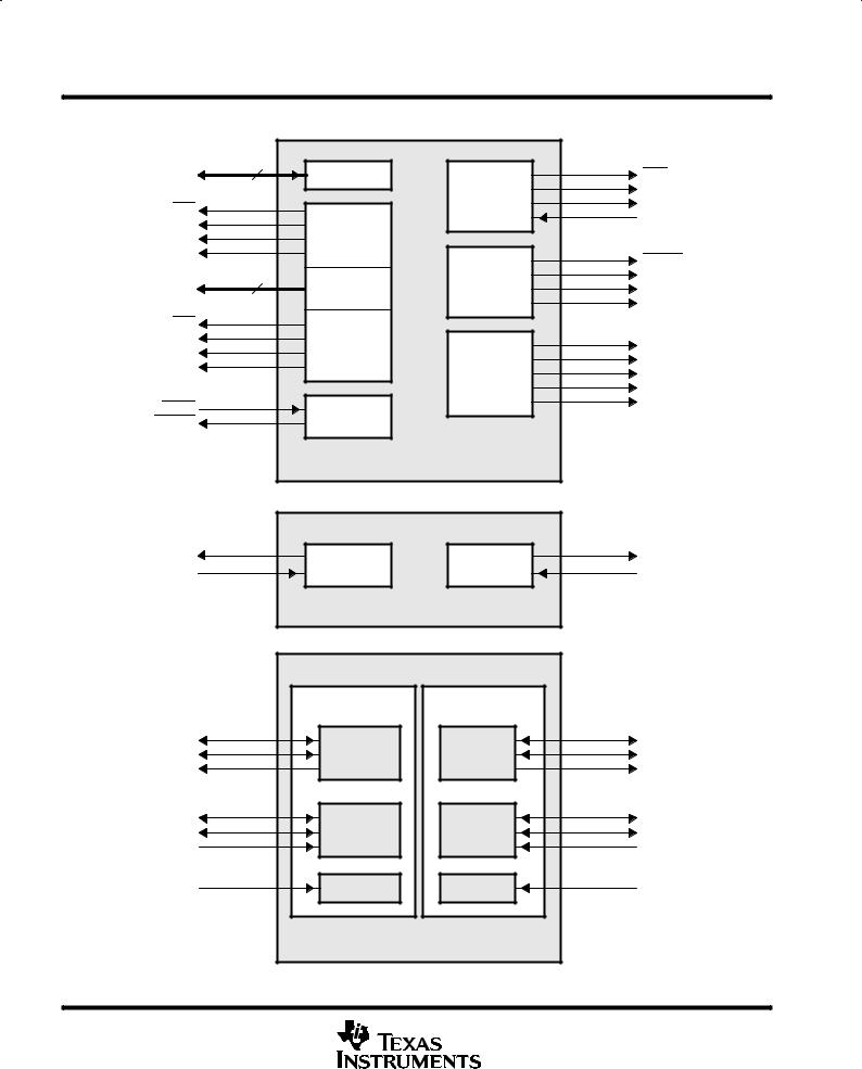
signal groups description
CLKIN
CLKOUT2  CLKOUT1
  Boot Mode
CLKMODE1 CLKMODE0
PLLFREQ3  Clock/PLL PLLFREQ2
PLLFREQ1 PLLV PLLG PLLF
Reset and
Interrupts
TMS
TDO 
TDI
TCK
JTAG
TRST
Emulation
EMU1 
EMU0 
 Little ENDIAN
Big ENDIAN
RSV9 |
|
|
RSV8 |
|
|
RSV7 |
DMA Status |
|
RSV6 |
||
|
||
RSV5 |
Reserved |
|
RSV4 |
||
RSV3 |
|
|
RSV2 |
Power-Down |
|
RSV1 |
||
Status |
||
RSV0 |
||
|
||
|
Control/Status |
|
16 |
|
HPI |
|
HD[15:0] |
Data |
(Host-Port Interface) |
||
|
||||
|
||||
|
|
|
|
HCNTL0
Register Select
HCNTL1
Control
HHWIL
HBE1
Half-Word/Byte
Select
HBE0
BOOTMODE4
BOOTMODE3
BOOTMODE2
BOOTMODE1
BOOTMODE0
RESET
NMI
EXT_INT7
EXT_INT6
EXT_INT5
EXT_INT4
IACK
INUM3
INUM2
INUM1
INUM0
LENDIAN
DMAC3
DMAC2
DMAC1
DMAC0
PD
HAS
HR/W
HCS
HDS1
HDS2
HRDY
HINT
Figure 3. CPU and Peripheral Signals
POST OFFICE BOX 1443 •HOUSTON, TEXAS 77251±1443 |
7 |
TMS320C6201, TMS320C6201B
DIGITAL SIGNAL PROCESSORS
SPRS051F ± JANUARY 1997 ± REVISED AUGUST 1999
signal groups description (continued)
ED[31:0] |
32 |
|
|
|
Data |
Asynchronous |
ARE |
||
|
|
AOE |
||
|
|
Memory |
||
CE3 |
|
AWE |
||
|
Control |
|||
|
ARDY |
|||
CE2 |
|
|||
|
|
|||
Memory Map |
|
|
||
CE1 |
|
|
||
Space Select |
|
|
||
CE0 |
|
|
||
|
|
SSADS |
||
|
|
|
||
|
20 |
SBSRAM |
SSOE |
|
EA[21:2] |
Control |
SSWE |
||
Word Address |
||||
|
|
|
SSCLK |
|
BE3 |
|
|
|
|
BE2 |
Byte Enables |
|
SDA10 |
|
BE1 |
|
|||
|
SDRAM |
SDRAS |
||
BE0 |
|
|||
|
SDCAS |
|||
|
|
Control |
||
|
|
|
SDWE |
|
HOLD |
HOLD/ |
|
SDCLK |
|
|
|
|||
HOLDA |
HOLDA |
|
|
|
|
|
EMIF |
|
|
|
|
(External Memory Interface) |
|
TOUT1 |
Timer 1 |
Timer 0 |
TOUT0 |
|
TINP1 |
TINP0 |
|||
|
|
|||
|
|
Timers |
|
|
|
McBSP1 |
McBSP0 |
|
|
CLKX1 |
|
|
CLKX0 |
|
FSX1 |
Transmit |
Transmit |
FSX0 |
|
DX1 |
|
|
DX0 |
|
CLKR1 |
|
|
CLKR0 |
|
FSR1 |
Receive |
Receive |
FSR0 |
|
DR1 |
|
|
DR0 |
|
CLKS1 |
Clock |
Clock |
CLKS0 |
|
|
|
McBSPs |
|
|
|
(Multichannel Buffered Serial Ports) |
|
||
Figure 4. Peripheral Signals
8 |
POST OFFICE BOX 1443 •HOUSTON, TEXAS 77251±1443 |

|
|
|
|
|
|
|
TMS320C6201, TMS320C6201B |
|
|
|
|
|
|
|
|
DIGITAL SIGNAL PROCESSORS |
|
|
|
|
|
|
|
|
SPRS051F ± JANUARY 1997 ± REVISED AUGUST 1999 |
|
|
|
|
|
|
|
|
|
|
|
|
|
|
|
|
|
Signal Descriptions |
|
|
|
|
|
|
|
|
|
|
|
|
|
|
SIGNAL |
|
|
|
|
|
NAME |
GGP, GJC |
GJL |
TYPE² |
DESCRIPTION |
|
||
|
PIN NO. |
PIN NO. |
|
|
|
|||
|
|
|
|
|
|
|
||
|
|
|
|
|
|
|
|
|
|
|
|
|
|
|
|
CLOCK/PLL |
|
|
|
|
|
|
|
|
|
|
|
CLKIN |
C10 |
B9 |
I |
Clock Input |
|
||
|
|
|
|
|
|
|
|
|
|
CLKOUT1 |
AF22 |
AC18 |
O |
Clock output at full device speed |
|
||
|
|
|
|
|
|
|
|
|
|
CLKOUT2 |
AF20 |
AC16 |
O |
Clock output at half of device speed |
|
||
|
|
|
|
|
|
|
|
|
|
CLKMODE1 |
C6 |
D8 |
I |
Clock-mode select |
|
||
|
|
|
|
|
|
• Selects whether the CPU clock frequency = input clock frequency x4 or x1 |
|
|
|
CLKMODE0 |
C5 |
C7 |
|
||||
|
|
|
||||||
|
|
|
|
|
|
|
|
|
|
PLLFREQ3 |
A9 |
A9 |
|
PLL frequency range (3, 2, and 1) |
|
||
|
|
|
|
|
|
|
• The target range for CLKOUT1 frequency is determined by the 3-bit value of the |
|
|
PLLFREQ2 |
D11 |
D11 |
I |
|
|||
|
PLLFREQ pins. |
|
||||||
|
|
|
|
|
|
|
|
|
|
|
|
|
|
|
|
|
|
|
PLLFREQ1 |
B10 |
B10 |
|
|
|
||
|
|
|
|
|
|
|
|
|
|
PLLV³ |
D12 |
B11 |
A§ |
PLL analog VCC connection for the low-pass filter |
|
||
|
PLLG³ |
C12 |
C12 |
A§ |
PLL analog GND connection for the low-pass filter |
|
||
|
PLLF |
A11 |
D12 |
A§ |
PLL low-pass filter connection to external components and a bypass capacitor |
|
||
|
|
|
|
|
|
|
JTAG EMULATION |
|
|
|
|
|
|
|
|
|
|
|
TMS |
L3 |
L3 |
I |
JTAG test port mode select (features an internal pullup) |
|
||
|
|
|
|
|
|
|
|
|
|
TDO |
W2 |
U4 |
O/Z |
JTAG test port data out |
|
||
|
|
|
|
|
|
|
|
|
|
TDI |
R4 |
T2 |
I |
JTAG test port data in (features an internal pullup) |
|
||
|
|
|
|
|
|
|
|
|
|
TCK |
R3 |
R3 |
I |
JTAG test port clock |
|
||
|
|
|
|
|
|
|
|
|
|
|
|
|
T1 |
R4 |
I |
JTAG test port reset (features an internal pulldown) |
|
|
TRST |
|
|
|
||||
|
|
|
|
|
|
|
|
|
|
EMU1 |
Y1 |
V3 |
I/O/Z |
Emulation pin 1, pullup with a dedicated 20-kΩ resistor¶ |
|
||
|
EMU0 |
W3 |
W2 |
I/O/Z |
Emulation pin 0, pullup with a dedicated 20-kΩ resistor¶ |
|
||
|
|
|
|
|
|
|
RESET AND INTERRUPTS |
|
|
|
|
|
|
|
|
||
|
RESET |
|
K2 |
K2 |
I |
Device reset |
|
|
|
|
|
|
|
|
|
|
|
|
NMI |
L2 |
L2 |
I |
Nonmaskable interrupt |
|
||
|
• Edge-driven (rising edge) |
|
||||||
|
|
|
|
|
|
|
|
|
|
|
|
|
|
|
|
||
|
EXT_INT7 |
U3 |
U2 |
|
|
|
||
|
|
|
|
|
|
|
||
|
EXT_INT6 |
V2 |
T4 |
I |
External interrupts |
|
||
|
EXT_INT5 |
W1 |
V1 |
• Edge-driven (rising edge) |
|
|||
|
|
|
||||||
|
|
|
|
|
|
|
||
|
EXT_INT4 |
U4 |
V2 |
|
|
|
||
|
|
|
|
|
|
|
||
|
IACK |
Y2 |
Y1 |
O |
Interrupt acknowledge for all active interrupts serviced by the CPU |
|
||
|
|
|
|
|
|
|
||
|
INUM3 |
AA1 |
V4 |
|
|
|
||
|
|
|
|
|
|
|
Active interrupt identification number |
|
|
INUM2 |
W4 |
Y2 |
|
|
|||
|
O |
• Valid during IACK for all active interrupts (not just external) |
|
|||||
|
|
|
|
|
|
|
||
|
INUM1 |
AA2 |
AA1 |
|
||||
|
|
• Encoding order follows the interrupt-service fetch-packet ordering |
|
|||||
|
|
|
|
|
|
|
|
|
|
INUM0 |
AB1 |
W4 |
|
|
|
||
|
|
|
|
|
|
|
|
|
|
|
|
|
|
|
|
LITTLE ENDIAN/BIG ENDIAN |
|
|
|
|
|
|
|
|
|
|
|
LENDIAN |
H3 |
G2 |
I |
If high, LENDIAN selects little-endian byte/half-word addressing order within a word |
|
||
|
If low, LENDIAN selects big-endian addressing |
|
||||||
|
|
|
|
|
|
|
|
|
|
|
|
|
|
|
|
|
|
|
|
|
|
|
|
|
POWER-DOWN STATUS |
|
|
|
|
|
|
|
|
||
|
PD |
D3 |
E2 |
O |
Power-down mode 2 or 3 (active if high) |
|
||
² I = Input, O = Output, Z = High Impedance, S = Supply Voltage, GND = Ground
³ PLLV and PLLG are not part of external voltage supply or ground. See the clock PLL section for information on how to connect these pins. § A = Analog Signal (PLL Filter)
¶For emulation and normal operation, pull up EMU1 and EMU0 with a dedicated 20-kΩ resistor. For boundary scan, pull down EMU1 and EMU0 with a dedicated 20-kΩ resistor.
POST OFFICE BOX 1443 •HOUSTON, TEXAS 77251±1443 |
9 |

TMS320C6201, TMS320C6201B
DIGITAL SIGNAL PROCESSORS
SPRS051F ± JANUARY 1997 ± REVISED AUGUST 1999
Signal Descriptions (Continued)
|
|
|
|
|
|
|
|
|
|
SIGNAL |
|
|
|
|
|
NAME |
GGP, GJC |
GJL |
TYPE² |
DESCRIPTION |
|||||||
|
|
PIN NO. |
PIN NO. |
|
|
||||||||
|
|
|
|
|
|
|
|
|
|
|
|
||
|
|
|
|
|
|
|
|
|
|
|
|
|
|
|
|
|
|
|
|
|
|
|
|
|
|
|
HOST-PORT INTERFACE (HPI) |
|
|
|
|
|
|
|
|
|
|
|
|
|
|
|
HINT |
|
|
|
|
|
H26 |
J26 |
O |
Host interrupt (from DSP to host) |
|||
|
|
|
|
|
|
|
|
|
|
|
|
|
|
|
HCNTL1 |
F23 |
G24 |
I |
Host control ± selects between control, address, or data registers |
||||||||
|
|
|
|
|
|
|
|
|
|
|
|
|
|
|
HCNTL0 |
D25 |
F25 |
I |
Host control ± selects between control, address, or data registers |
||||||||
|
|
|
|
|
|
|
|
|
|
|
|
|
|
|
HHWIL |
C26 |
E26 |
I |
Host half-word select ± first or second half-word (not necessarily high or low order) |
||||||||
|
|
|
|
|
|
|
|
|
|
|
|
||
|
|
|
|
|
|
|
|
|
|
E23 |
F24 |
I |
Host byte select within word or half-word |
|
HBE1 |
|
|
|
|
||||||||
|
|
|
|
|
|
|
|
|
|
|
|
||
|
|
|
|
|
|
|
|
|
|
D24 |
E25 |
I |
Host byte select within word or half-word |
|
HBE0 |
|
|
|
|
||||||||
|
|
|
|
|
|
|
|
|
|
C23 |
B22 |
I |
Host read or write select |
|
HR/W |
|
|
|
|||||||||
|
|
|
|
|
|
|
|
|
|
||||
|
HD15 |
B13 |
A12 |
|
|
||||||||
|
|
|
|
|
|
|
|
|
|
||||
|
HD14 |
B14 |
D13 |
|
|
||||||||
|
|
|
|
|
|
|
|
|
|
||||
|
HD13 |
C14 |
C13 |
|
|
||||||||
|
|
|
|
|
|
|
|
|
|
||||
|
HD12 |
B15 |
D14 |
|
|
||||||||
|
|
|
|
|
|
|
|
|
|
||||
|
HD11 |
D15 |
B15 |
|
|
||||||||
|
|
|
|
|
|
|
|
|
|
||||
|
HD10 |
B16 |
C15 |
|
|
||||||||
|
|
|
|
|
|
|
|
|
|
||||
|
HD9 |
A17 |
D15 |
|
|
||||||||
|
|
|
|
|
|
|
|
|
|
||||
|
HD8 |
B17 |
B16 |
I/O/Z |
Host-port data (used for transfer of data, address, and control) |
||||||||
|
|
|
|
|
|
|
|
|
|
|
|
||
|
HD7 |
D16 |
C16 |
||||||||||
|
|
|
|||||||||||
|
|
|
|
|
|
|
|
|
|
||||
|
HD6 |
B18 |
B17 |
|
|
||||||||
|
|
|
|
|
|
|
|
|
|
||||
|
HD5 |
A19 |
D16 |
|
|
||||||||
|
|
|
|
|
|
|
|
|
|
||||
|
HD4 |
C18 |
A18 |
|
|
||||||||
|
|
|
|
|
|
|
|
|
|
||||
|
HD3 |
B19 |
B18 |
|
|
||||||||
|
|
|
|
|
|
|
|
|
|
||||
|
HD2 |
C19 |
D17 |
|
|
||||||||
|
|
|
|
|
|
|
|
|
|
||||
|
HD1 |
B20 |
C18 |
|
|
||||||||
|
|
|
|
|
|
|
|
|
|
||||
|
HD0 |
B21 |
A20 |
|
|
||||||||
|
|
|
|
|
|
|
|
|
|||||
|
|
|
|
|
|
|
|
|
|
C22 |
C20 |
I |
Host address strobe |
|
HAS |
|
|
|
|
||||||||
|
|
|
|
|
|
|
|
||||||
|
|
|
|
|
|
|
|
|
|
B23 |
B21 |
I |
Host chip select |
|
HCS |
|
|
|
|||||||||
|
|
|
|
|
|
|
|
||||||
|
|
|
|
|
|
|
|
|
|
D22 |
C21 |
I |
Host data strobe 1 |
|
HDS1 |
|
|
|
|||||||||
|
|
|
|
|
|
|
|||||||
|
|
|
|
|
|
|
|
|
|
A24 |
D20 |
I |
Host data strobe 2 |
|
HDS2 |
|
|
||||||||||
|
|
|
|
|
|
||||||||
|
|
|
|
|
|
|
|
|
|
J24 |
J25 |
O |
Host ready (from DSP to host) |
|
HRDY |
|
|||||||||||
|
|
|
|
|
|
|
|
|
|
|
|
|
|
|
|
|
|
|
|
|
|
|
|
|
|
|
BOOT MODE |
|
|
|
|
|
|
||||||||
|
BOOTMODE4 |
D8 |
C8 |
|
|
||||||||
|
|
|
|
|
|
||||||||
|
BOOTMODE3 |
B4 |
B6 |
|
|
||||||||
|
|
|
|
I |
Boot mode |
||||||||
|
BOOTMODE2 |
A3 |
D7 |
||||||||||
|
|
|
|
|
|
||||||||
|
BOOTMODE1 |
D5 |
C6 |
|
|
||||||||
|
|
|
|
|
|
||||||||
|
BOOTMODE0 |
C4 |
B5 |
|
|
||||||||
² I = Input, O = Output, Z = High Impedance, S = Supply Voltage, GND = Ground
10 |
POST OFFICE BOX 1443 •HOUSTON, TEXAS 77251±1443 |
|
|
|
|
|
|
|
|
TMS320C6201, TMS320C6201B |
|
|
|
|
|
|
|
|
|
DIGITAL SIGNAL PROCESSORS |
|
|
|
|
|
|
|
|
|
SPRS051F ± JANUARY 1997 ± REVISED AUGUST 1999 |
|
|
|
|
|
|
|
|
|
|
|
|
|
|
|
|
|
|
Signal Descriptions (Continued) |
||
|
|
|
|
|
|
|
|
|
|
|
|
|
|
|
SIGNAL |
|
|
|
|
|
NAME |
GGP, GJC |
GJL |
TYPE² |
DESCRIPTION |
|
|||
|
PIN NO. |
PIN NO. |
|
|
|
||||
|
|
|
|
|
|
|
|
||
|
|
|
|
|
|
|
|
|
|
|
|
|
|
|
|
EMIF ± CONTROL SIGNALS COMMON TO ALL TYPES OF MEMORY |
|
||
|
|
|
|
|
|
|
|
|
|
|
CE3 |
|
|
AE22 |
AD20 |
|
|
|
|
|
|
|
|
|
|
|
|
||
|
|
|
|
|
AD26 |
AA24 |
|
Memory space enables |
|
|
CE2 |
|
O/Z |
|
|||||
|
|
|
|
|
|
|
• Enabled by bits 24 and 25 of the word address |
|
|
|
|
|
|
|
|
|
|
||
|
CE1 |
AB24 |
AB26 |
|
|||||
|
|
|
|||||||
|
|
|
|
|
|
• Only one asserted during any external data access |
|
||
|
|
|
|
|
AC26 |
AA25 |
|
|
|
|
CE0 |
|
|
|
|||||
|
|
|
|
|
|
|
|
||
|
|
|
|
|
AB25 |
Y24 |
|
Byte-enable control |
|
|
BE3 |
|
|
|
|||||
|
|
|
|
|
|
• Decoded from the two lowest bits of the internal address |
|
||
|
|
|
|
|
AA24 |
W23 |
|
|
|
|
BE2 |
|
O/Z |
|
|||||
|
|
|
|
|
|
|
• Byte-write enables for most types of memory |
|
|
|
|
|
|
|
|
|
|
||
|
BE1 |
Y23 |
AA26 |
|
|||||
|
|
|
|||||||
|
|
|
|
|
• Can be directly connected to SDRAM read and write mask signal (SDQM) |
|
|||
|
|
|
|
|
AA26 |
W25 |
|
|
|
|
BE0 |
|
|
|
|||||
|
|
|
|
|
|
|
|
|
|
|
|
|
|
|
|
|
|
EMIF ± ADDRESS |
|
|
|
|
|
|
|
|
|||
|
EA21 |
J26 |
K25 |
|
|
|
|||
|
|
|
|
|
|
|
|||
|
EA20 |
K25 |
L24 |
|
|
|
|||
|
|
|
|
|
|
|
|||
|
EA19 |
L24 |
L25 |
|
|
|
|||
|
|
|
|
|
|
|
|||
|
EA18 |
K26 |
M23 |
|
|
|
|||
|
|
|
|
|
|
|
|||
|
EA17 |
M26 |
M25 |
|
|
|
|||
|
|
|
|
|
|
|
|||
|
EA16 |
M25 |
M24 |
|
|
|
|||
|
|
|
|
|
|
|
|||
|
EA15 |
P25 |
N23 |
|
|
|
|||
|
|
|
|
|
|
|
|||
|
EA14 |
P24 |
P24 |
|
|
|
|||
|
|
|
|
|
|
|
|||
|
EA13 |
R25 |
P23 |
|
|
|
|||
|
|
|
|
|
|
|
|||
|
EA12 |
T26 |
R25 |
O/Z |
External address (word address) |
|
|||
|
|
|
|
|
|
|
|
||
|
EA11 |
R23 |
R24 |
|
|||||
|
|
|
|
||||||
|
|
|
|
|
|
|
|||
|
EA10 |
U26 |
R23 |
|
|
|
|||
|
|
|
|
|
|
|
|||
|
EA9 |
U25 |
T25 |
|
|
|
|||
|
|
|
|
|
|
|
|||
|
EA8 |
T23 |
T24 |
|
|
|
|||
|
|
|
|
|
|
|
|||
|
EA7 |
V26 |
U25 |
|
|
|
|||
|
|
|
|
|
|
|
|||
|
EA6 |
V25 |
T23 |
|
|
|
|||
|
|
|
|
|
|
|
|||
|
EA5 |
W26 |
V26 |
|
|
|
|||
|
|
|
|
|
|
|
|||
|
EA4 |
V24 |
V25 |
|
|
|
|||
|
|
|
|
|
|
|
|||
|
EA3 |
W25 |
U23 |
|
|
|
|||
|
|
|
|
|
|
|
|||
|
EA2 |
Y26 |
V24 |
|
|
|
|||
² I = Input, O = Output, Z = High Impedance, S = Supply Voltage, GND = Ground
POST OFFICE BOX 1443 •HOUSTON, TEXAS 77251±1443 |
11 |

TMS320C6201, TMS320C6201B
DIGITAL SIGNAL PROCESSORS
SPRS051F ± JANUARY 1997 ± REVISED AUGUST 1999
Signal Descriptions (Continued)
|
|
|
|
|
SIGNAL |
|
|
|
|
NAME |
GGP, GJC |
GJL |
TYPE² |
DESCRIPTION |
|||
|
PIN NO. |
PIN NO. |
|
|
||||
|
|
|
|
|
|
|
||
|
|
|
|
|
|
|
|
|
|
|
|
|
|
|
|
|
EMIF ± DATA |
|
|
|
|
|
|
|
|
|
|
ED31 |
AB2 |
Y3 |
|
|
|||
|
|
|
|
|
|
|
|
|
|
ED30 |
AC1 |
AA2 |
|
|
|||
|
|
|
|
|
|
|
|
|
|
ED29 |
AA4 |
AB1 |
|
|
|||
|
|
|
|
|
|
|
|
|
|
ED28 |
AD1 |
AA3 |
|
|
|||
|
|
|
|
|
|
|
|
|
|
ED27 |
AC3 |
AB2 |
|
|
|||
|
|
|
|
|
|
|
|
|
|
ED26 |
AD4 |
AE5 |
|
|
|||
|
|
|
|
|
|
|
|
|
|
ED25 |
AF3 |
AD6 |
|
|
|||
|
|
|
|
|
|
|
|
|
|
ED24 |
AE4 |
AC7 |
|
|
|||
|
|
|
|
|
|
|
|
|
|
ED23 |
AD5 |
AE6 |
|
|
|||
|
|
|
|
|
|
|
|
|
|
ED22 |
AF4 |
AD7 |
|
|
|||
|
|
|
|
|
|
|
|
|
|
ED21 |
AE5 |
AC8 |
|
|
|||
|
|
|
|
|
|
|
|
|
|
ED20 |
AD6 |
AD8 |
|
|
|||
|
|
|
|
|
|
|
|
|
|
ED19 |
AE6 |
AC9 |
|
|
|||
|
|
|
|
|
|
|
|
|
|
ED18 |
AD7 |
AF7 |
|
|
|||
|
|
|
|
|
|
|
|
|
|
ED17 |
AC8 |
AD9 |
|
|
|||
|
|
|
|
|
|
|
|
|
|
ED16 |
AF7 |
AC10 |
I/O/Z |
External data |
|||
|
|
|
|
|
|
|
||
|
ED15 |
AD9 |
AE9 |
|||||
|
|
|
||||||
|
|
|
|
|
|
|
|
|
|
ED14 |
AD10 |
AF9 |
|
|
|||
|
|
|
|
|
|
|
|
|
|
ED13 |
AF9 |
AC11 |
|
|
|||
|
|
|
|
|
|
|
|
|
|
ED12 |
AC11 |
AE10 |
|
|
|||
|
|
|
|
|
|
|
|
|
|
ED11 |
AE10 |
AD11 |
|
|
|||
|
|
|
|
|
|
|
|
|
|
ED10 |
AE11 |
AE11 |
|
|
|||
|
|
|
|
|
|
|
|
|
|
ED9 |
AF11 |
AC12 |
|
|
|||
|
|
|
|
|
|
|
|
|
|
ED8 |
AE14 |
AD12 |
|
|
|||
|
|
|
|
|
|
|
|
|
|
ED7 |
AF15 |
AE12 |
|
|
|||
|
|
|
|
|
|
|
|
|
|
ED6 |
AE15 |
AC13 |
|
|
|||
|
|
|
|
|
|
|
|
|
|
ED5 |
AF16 |
AD14 |
|
|
|||
|
|
|
|
|
|
|
|
|
|
ED4 |
AC15 |
AC14 |
|
|
|||
|
|
|
|
|
|
|
|
|
|
ED3 |
AE17 |
AE15 |
|
|
|||
|
|
|
|
|
|
|
|
|
|
ED2 |
AF18 |
AD15 |
|
|
|||
|
|
|
|
|
|
|
|
|
|
ED1 |
AF19 |
AE16 |
|
|
|||
|
|
|
|
|
|
|
|
|
|
ED0 |
AC17 |
AD16 |
|
|
|||
|
|
|
|
|
|
|
|
|
|
|
|
|
|
|
|
EMIF ± ASYNCHRONOUS MEMORY CONTROL |
|
|
|
|
|
|
|
|
|
|
|
ARE |
|
|
|
Y24 |
V23 |
O/Z |
Asynchronous memory read enable |
|
|
|
|
|
|
|
||
|
|
|
|
|
AC24 |
AB25 |
O/Z |
Asynchronous memory output enable |
|
AOE |
|
|
|||||
|
|
|
|
|
|
|||
|
|
|
|
|
AD23 |
AE22 |
O/Z |
Asynchronous memory write enable |
|
AWE |
|
||||||
|
|
|
|
|
|
|||
|
ARDY |
W23 |
Y26 |
I |
Asynchronous memory ready input |
|||
² I = Input, O = Output, Z = High Impedance, S = Supply Voltage, GND = Ground
12 |
POST OFFICE BOX 1443 •HOUSTON, TEXAS 77251±1443 |

|
|
|
|
|
|
|
|
|
|
|
|
|
TMS320C6201, TMS320C6201B |
|
|
|
|
|
|
|
|
|
|
|
|
|
|
DIGITAL SIGNAL PROCESSORS |
|
|
|
|
|
|
|
|
|
|
|
|
|
|
SPRS051F ± JANUARY 1997 ± REVISED AUGUST 1999 |
|
|
|
|
|
|
|
|
|
|
|
|
|
|
|
|
|
|
|
|
|
|
|
|
|
|
|
|
Signal Descriptions (Continued) |
||
|
|
|
|
|
|
|
|
|
|
|
|
|
|
|
|
|
|
|
|
|
|
|
|
SIGNAL |
|
|
|
|
|
|
NAME |
GGP, GJC |
GJL |
|
TYPE² |
DESCRIPTION |
|
|||||||
|
PIN NO. |
PIN NO. |
|
|
|
|
||||||||
|
|
|
|
|
|
|
|
|
|
|
|
|
||
|
|
|
|
|
|
|
|
|
|
|
|
|
|
|
|
|
|
|
|
|
|
|
|
|
EMIF ± SYNCHRONOUS BURST SRAM (SBSRAM) CONTROL |
|
|||
|
|
|
|
|
|
|
|
|
|
|
|
|
|
|
|
SSADS |
|
|
|
AC20 |
AD19 |
|
O/Z |
SBSRAM address strobe |
|
||||
|
|
|
|
|
|
|
|
|
|
|
|
|
||
|
|
|
|
|
|
|
|
|
AF21 |
AD18 |
|
O/Z |
SBSRAM output enable |
|
|
SSOE |
|
|
|
|
|
|
|
||||||
|
|
|
|
|
|
|
|
|
|
|
|
|||
|
|
|
|
|
|
|
|
|
AD19 |
AF18 |
|
O/Z |
SBSRAM write enable |
|
|
SSWE |
|
|
|
|
|
|
|||||||
|
|
|
|
|
|
|
|
|
|
|
|
|||
|
SSCLK |
AD17 |
AC15 |
|
O |
SBSRAM clock |
|
|||||||
|
|
|
|
|
|
|
|
|
|
|
|
|
|
|
|
|
|
|
|
|
|
|
|
|
|
EMIF ± SYNCHRONOUS DRAM (SDRAM) CONTROL |
|
||
|
|
|
|
|
|
|
|
|
|
|
|
|||
|
SDA10 |
AD21 |
AC19 |
|
O/Z |
SDRAM address 10 (separate for deactivate command) |
|
|||||||
|
|
|
|
|
|
|
|
|
|
|
||||
|
|
|
|
|
|
|
|
|
AF24 |
AD21 |
|
O/Z |
SDRAM row-address strobe |
|
|
SDRAS |
|
|
|
|
|||||||||
|
|
|
|
|
|
|
|
|
|
|||||
|
|
|
|
|
|
|
|
|
AD22 |
AC20 |
|
O/Z |
SDRAM column-address strobe |
|
|
SDCAS |
|
|
|
||||||||||
|
|
|
|
|
|
|
|
|
||||||
|
|
|
|
|
|
|
|
|
AF23 |
AE21 |
|
O/Z |
SDRAM write enable |
|
|
SDWE |
|
|
|
||||||||||
|
|
|
|
|
|
|
|
|
||||||
|
SDCLK |
AE20 |
AC17 |
|
O |
SDRAM clock |
|
|||||||
|
|
|
|
|
|
|
|
|
|
|
|
|
|
|
|
|
|
|
|
|
|
|
|
|
|
|
|
EMIF ± BUS ARBITRATION |
|
|
|
|
|
|
|
|
|
|||||||
|
HOLD |
|
AA25 |
Y25 |
|
I |
Hold request from the host |
|
||||||
|
|
|
|
|
|
|
|
|||||||
|
|
|
|
|
|
|
|
|
A7 |
C9 |
|
O |
Hold-request acknowledge to the host |
|
|
HOLDA |
|
|
|
||||||||||
|
|
|
|
|
|
|
|
|
|
|
|
|
|
|
|
|
|
|
|
|
|
|
|
|
|
|
|
TIMERS |
|
|
|
|
|
|
|
|
|
|||||||
|
TOUT1 |
H24 |
K23 |
|
O |
Timer 1 or general-purpose output |
|
|||||||
|
|
|
|
|
|
|
|
|||||||
|
TINP1 |
K24 |
L23 |
|
I |
Timer 1 or general-purpose input |
|
|||||||
|
|
|
|
|
|
|
|
|||||||
|
TOUT0 |
M4 |
M4 |
|
O |
Timer 0 or general-purpose output |
|
|||||||
|
|
|
|
|
|
|
|
|||||||
|
TINP0 |
K4 |
H2 |
|
I |
Timer 0 or general-purpose input |
|
|||||||
|
|
|
|
|
|
|
|
|
|
|
|
|
|
|
|
|
|
|
|
|
|
|
|
|
|
|
DMA ACTION COMPLETE STATUS |
|
|
|
|
|
|
|
|
|
|
|||||||
|
DMAC3 |
D2 |
E1 |
|
|
|
|
|||||||
|
|
|
|
|
|
|
|
|||||||
|
DMAC2 |
F4 |
F2 |
|
O |
DMA action complete |
|
|||||||
|
|
|
|
|
|
|
|
|
|
|
|
|
||
|
DMAC1 |
D1 |
G3 |
|
|
|||||||||
|
|
|
|
|
||||||||||
|
|
|
|
|
|
|
|
|||||||
|
DMAC0 |
E2 |
H4 |
|
|
|
|
|||||||
|
|
|
|
|
|
|
|
|
|
|
|
|
|
|
|
|
|
|
|
|
|
|
|
|
MULTICHANNEL BUFFERED SERIAL PORT 1 (McBSP1) |
|
|||
|
|
|
|
|
|
|
|
|||||||
|
CLKS1 |
E25 |
F26 |
|
I |
External clock source (as opposed to internal) |
|
|||||||
|
|
|
|
|
|
|
|
|||||||
|
CLKR1 |
H23 |
H25 |
|
I/O/Z |
Receive clock |
|
|||||||
|
|
|
|
|
|
|
|
|||||||
|
CLKX1 |
F26 |
J24 |
|
I/O/Z |
Transmit clock |
|
|||||||
|
|
|
|
|
|
|
|
|||||||
|
DR1 |
D26 |
H23 |
|
I |
Receive data |
|
|||||||
|
|
|
|
|
|
|
|
|||||||
|
DX1 |
G23 |
G25 |
|
O/Z |
Transmit data |
|
|||||||
|
|
|
|
|
|
|
|
|||||||
|
FSR1 |
E26 |
J23 |
|
I/O/Z |
Receive frame sync |
|
|||||||
|
|
|
|
|
|
|
|
|||||||
|
FSX1 |
F25 |
G26 |
|
I/O/Z |
Transmit frame sync |
|
|||||||
² I = Input, O = Output, Z = High Impedance, S = Supply Voltage, GND = Ground
POST OFFICE BOX 1443 •HOUSTON, TEXAS 77251±1443 |
13 |

TMS320C6201, TMS320C6201B
DIGITAL SIGNAL PROCESSORS
SPRS051F ± JANUARY 1997 ± REVISED AUGUST 1999
Signal Descriptions (Continued)
|
SIGNAL |
|
|
|
NAME |
GGP, GJC |
GJL |
TYPE² |
DESCRIPTION |
PIN NO. |
PIN NO. |
|
|
|
|
|
|
||
|
|
|
|
|
|
|
MULTICHANNEL BUFFERED SERIAL PORT 0 (McBSP0) |
||
|
|
|
|
|
CLKS0 |
L4 |
L4 |
I |
External clock source (as opposed to internal) |
|
|
|
|
|
CLKR0 |
M2 |
M2 |
I/O/Z |
Receive clock |
|
|
|
|
|
CLKX0 |
L1 |
M3 |
I/O/Z |
Transmit clock |
|
|
|
|
|
DR0 |
J1 |
J1 |
I |
Receive data |
|
|
|
|
|
DX0 |
R1 |
P4 |
O/Z |
Transmit data |
|
|
|
|
|
FSR0 |
P4 |
N3 |
I/O/Z |
Receive frame sync |
|
|
|
|
|
FSX0 |
P3 |
N4 |
I/O/Z |
Transmit frame sync |
|
|
|
|
|
|
|
|
|
RESERVED FOR TEST |
|
|
|
|
|
RSV0 |
T2 |
T3 |
I |
Reserved for testing, pullup with a dedicated 20-kΩ resistor |
RSV1 |
G2 |
F1 |
I |
Reserved for testing, pullup with a dedicated 20-kΩ resistor |
|
|
|
|
|
RSV2 |
C11 |
C11 |
I |
Reserved for testing, pullup with a dedicated 20-kΩ resistor |
RSV3 |
B9 |
D10 |
I |
Reserved for testing, pullup with a dedicated 20-kΩ resistor |
|
|
|
|
|
RSV4 |
A6 |
D9 |
I |
Reserved for testing, pulldown with a dedicated 20-kΩ resistor |
|
|
|
|
|
RSV5 |
C8 |
A7 |
O |
Reserved (leave unconnected, do not connect to power or ground) |
|
|
|
|
|
RSV6 |
C21 |
D18 |
I |
Reserved for testing, pullup with a dedicated 20-kW resistor |
|
|
|
|
|
RSV7 |
B22 |
C19 |
I |
Reserved for testing, pullup with a dedicated 20-kW resistor |
|
|
|
|
|
RSV8 |
A23 |
D19 |
I |
Reserved for testing, pullup with a dedicated 20-kW resistor |
|
|
|
|
|
RSV9 |
E4 |
F3 |
O |
Reserved (leave unconnected, do not connect to power or ground) |
|
|
|
|
|
|
|
|
|
UNCONNECTED PINS |
|
|
|
|
|
|
A8 |
AF20 |
|
|
|
|
|
|
|
|
B8 |
AE18 |
|
|
|
|
|
|
|
|
C9 |
AE17 |
|
|
|
|
|
|
|
|
D10 |
± |
|
|
|
|
|
|
|
|
D21 |
± |
|
|
NC |
|
|
|
Unconnected pins |
G1 |
J4 |
|
||
|
|
|
|
|
|
H1 |
J3 |
|
|
|
|
|
|
|
|
H2 |
G1 |
|
|
|
|
|
|
|
|
J2 |
K4 |
|
|
|
|
|
|
|
|
K3 |
J2 |
|
|
|
|
|
|
|
|
R2 |
R2 |
|
|
² I = Input, O = Output, Z = High Impedance, S = Supply Voltage, GND = Ground
14 |
POST OFFICE BOX 1443 •HOUSTON, TEXAS 77251±1443 |

|
|
|
|
TMS320C6201, TMS320C6201B |
|
|
|
|
|
DIGITAL SIGNAL PROCESSORS |
|
|
|
|
|
SPRS051F ± JANUARY 1997 ± REVISED AUGUST 1999 |
|
|
|
|
|
|
|
|
|
|
Signal Descriptions (Continued) |
||
|
|
|
|
|
|
|
SIGNAL |
|
|
|
|
NAME |
GGP, GJC |
GJL |
TYPE² |
DESCRIPTION |
|
PIN NO. |
PIN NO. |
|
|
|
|
|
|
|
|
||
|
|
|
|
|
|
|
|
|
|
3.3-V SUPPLY VOLTAGE PINS |
|
|
|
|
|
|
|
|
A10 |
A5 |
|
|
|
|
|
|
|
|
|
|
A15 |
A11 |
|
|
|
|
|
|
|
|
|
|
A18 |
A16 |
|
|
|
|
|
|
|
|
|
|
A21 |
A22 |
|
|
|
|
|
|
|
|
|
|
A22 |
B7 |
|
|
|
|
|
|
|
|
|
|
B7 |
B8 |
|
|
|
|
|
|
|
|
|
|
C1 |
B19 |
|
|
|
|
|
|
|
|
|
|
D17 |
B20 |
|
|
|
|
|
|
|
|
|
|
F3 |
C10 |
|
|
|
|
|
|
|
|
|
|
G24 |
C14 |
|
|
|
|
|
|
|
|
|
|
G25 |
C17 |
|
|
|
|
|
|
|
|
|
|
H25 |
G4 |
|
|
|
|
|
|
|
|
|
|
J25 |
G23 |
|
|
|
|
|
|
|
|
|
|
L25 |
H3 |
|
|
|
|
|
|
|
|
|
|
M3 |
H24 |
|
|
|
|
|
|
|
|
|
|
N3 |
K3 |
|
|
|
|
|
|
|
|
|
|
N23 |
K24 |
|
|
|
|
|
|
|
|
|
|
R26 |
L1 |
|
|
|
|
|
|
|
|
|
|
T24 |
L26 |
|
|
|
|
|
|
|
|
|
DVDD |
U24 |
N24 |
S |
3.3-V supply voltage |
|
|
|
|
|||
W24 |
P3 |
|
|||
|
|
|
|
||
|
|
|
|
|
|
|
Y4 |
T1 |
|
|
|
|
|
|
|
|
|
|
AB3 |
T26 |
|
|
|
|
|
|
|
|
|
|
AB4 |
U3 |
|
|
|
|
|
|
|
|
|
|
AB26 |
U24 |
|
|
|
|
|
|
|
|
|
|
AC6 |
W3 |
|
|
|
|
|
|
|
|
|
|
AC10 |
W24 |
|
|
|
|
|
|
|
|
|
|
AC19 |
Y4 |
|
|
|
|
|
|
|
|
|
|
AC21 |
Y23 |
|
|
|
|
|
|
|
|
|
|
AC22 |
AD10 |
|
|
|
|
|
|
|
|
|
|
AC25 |
AD13 |
|
|
|
|
|
|
|
|
|
|
AD11 |
AD17 |
|
|
|
|
|
|
|
|
|
|
AD13 |
AE7 |
|
|
|
|
|
|
|
|
|
|
AD15 |
AE8 |
|
|
|
|
|
|
|
|
|
|
AD18 |
AE19 |
|
|
|
|
|
|
|
|
|
|
AE18 |
AE20 |
|
|
|
|
|
|
|
|
|
|
AE21 |
AF5 |
|
|
|
|
|
|
|
|
|
|
AF5 |
AF11 |
|
|
|
|
|
|
|
|
|
|
AF6 |
AF16 |
|
|
|
|
|
|
|
|
|
|
AF17 |
AF22 |
|
|
|
² I = Input, O = Output, Z = High Impedance, S = Supply Voltage, GND = Ground
POST OFFICE BOX 1443 •HOUSTON, TEXAS 77251±1443 |
15 |

TMS320C6201, TMS320C6201B
DIGITAL SIGNAL PROCESSORS
SPRS051F ± JANUARY 1997 ± REVISED AUGUST 1999
Signal Descriptions (Continued)
|
SIGNAL |
|
|
|
|
NAME |
GGP, GJC |
GJL |
TYPE² |
DESCRIPTION |
|
PIN NO. |
PIN NO. |
|
|
||
|
|
|
|||
|
|
|
|
|
|
|
|
|
2.5-V SUPPLY VOLTAGE PINS FOR 'C6201 |
||
|
|
|
1.8-V SUPPLY VOLTAGE PINS FOR 'C6201B |
||
|
|
|
|
|
|
|
A5 |
A1 |
|
|
|
|
|
|
|
|
|
|
A12 |
A2 |
|
|
|
|
|
|
|
|
|
|
A16 |
A3 |
|
|
|
|
|
|
|
|
|
|
A20 |
A24 |
|
|
|
|
|
|
|
|
|
|
B2 |
A25 |
|
|
|
|
|
|
|
|
|
|
B6 |
A26 |
|
|
|
|
|
|
|
|
|
|
B11 |
B1 |
|
|
|
|
|
|
|
|
|
|
B12 |
B2 |
|
|
|
|
|
|
|
|
|
|
B25 |
B3 |
|
|
|
|
|
|
|
|
|
|
C3 |
B24 |
|
|
|
|
|
|
|
|
|
|
C15 |
B25 |
|
|
|
|
|
|
|
|
|
|
C20 |
B26 |
|
|
|
|
|
|
|
|
|
|
C24 |
C1 |
|
|
|
|
|
|
|
|
|
|
D4 |
C2 |
|
|
|
|
|
|
|
|
|
|
D6 |
C3 |
|
|
|
|
|
|
|
|
|
|
D7 |
C4 |
|
|
|
|
|
|
|
|
|
|
D9 |
C23 |
|
|
|
|
|
|
|
|
|
|
D14 |
C24 |
|
|
|
|
|
|
|
|
|
CVDD |
D18 |
C25 |
S |
2.5-V supply voltage for 'C6201 |
|
D20 |
C26 |
1.8-V supply voltage for 'C6201B |
|||
|
|
||||
|
|
|
|
|
|
|
D23 |
D3 |
|
|
|
|
|
|
|
|
|
|
E1 |
D4 |
|
|
|
|
|
|
|
|
|
|
F1 |
D5 |
|
|
|
|
|
|
|
|
|
|
H4 |
D22 |
|
|
|
|
|
|
|
|
|
|
J4 |
D23 |
|
|
|
|
|
|
|
|
|
|
J23 |
D24 |
|
|
|
|
|
|
|
|
|
|
K1 |
E4 |
|
|
|
|
|
|
|
|
|
|
K23 |
E23 |
|
|
|
|
|
|
|
|
|
|
M1 |
AB4 |
|
|
|
|
|
|
|
|
|
|
M24 |
AB23 |
|
|
|
|
|
|
|
|
|
|
N4 |
AC3 |
|
|
|
|
|
|
|
|
|
|
N25 |
AC4 |
|
|
|
|
|
|
|
|
|
|
P2 |
AC5 |
|
|
|
|
|
|
|
|
|
|
P23 |
AC22 |
|
|
|
|
|
|
|
|
|
|
T3 |
AC23 |
|
|
|
|
|
|
|
|
|
|
T4 |
AC24 |
|
|
|
|
|
|
|
|
|
|
U1 |
AD1 |
|
|
|
|
|
|
|
|
|
|
V4 |
AD2 |
|
|
|
² I = Input, O = Output, Z = High Impedance, S = Supply Voltage, GND = Ground
16 |
POST OFFICE BOX 1443 •HOUSTON, TEXAS 77251±1443 |

|
|
|
|
TMS320C6201, TMS320C6201B |
|
|
|
|
|
DIGITAL SIGNAL PROCESSORS |
|
|
|
|
|
SPRS051F ± JANUARY 1997 ± REVISED AUGUST 1999 |
|
|
|
|
|
|
|
|
|
|
Signal Descriptions (Continued) |
||
|
|
|
|
|
|
|
SIGNAL |
|
|
|
|
NAME |
GGP, GJC |
GJL |
TYPE² |
DESCRIPTION |
|
PIN NO. |
PIN NO. |
|
|
|
|
|
|
|
|
||
|
|
|
|
|
|
|
|
|
2.5-V SUPPLY VOLTAGE PINS FOR 'C6201 |
|
|
|
|
1.8-V SUPPLY VOLTAGE PINS FOR 'C6201B (CONTINUED) |
|
||
|
|
|
|
|
|
|
V23 |
AD3 |
|
|
|
|
|
|
|
|
|
|
AC4 |
AD4 |
|
|
|
|
|
|
|
|
|
|
AC9 |
AD23 |
|
|
|
|
|
|
|
|
|
|
AC12 |
AD24 |
|
|
|
|
|
|
|
|
|
|
AC13 |
AD25 |
|
|
|
|
|
|
|
|
|
|
AC18 |
AD26 |
|
|
|
|
|
|
|
|
|
|
AC23 |
AE1 |
|
|
|
|
|
|
|
|
|
|
AD3 |
AE2 |
|
|
|
|
|
|
|
|
|
CVDD |
AD8 |
AE3 |
S |
2.5-V supply voltage for 'C6201 |
|
AD14 |
AE24 |
1.8-V supply voltage for 'C6201B |
|
||
|
|
|
|||
|
|
|
|
|
|
|
AD24 |
AE25 |
|
|
|
|
|
|
|
|
|
|
AE2 |
AE26 |
|
|
|
|
|
|
|
|
|
|
AE8 |
AF1 |
|
|
|
|
|
|
|
|
|
|
AE12 |
AF2 |
|
|
|
|
|
|
|
|
|
|
AE25 |
AF3 |
|
|
|
|
|
|
|
|
|
|
AF12 |
AF24 |
|
|
|
|
|
|
|
|
|
|
± |
AF25 |
|
|
|
|
|
|
|
|
|
|
± |
AF26 |
|
|
|
|
|
|
|
|
|
|
|
|
|
GROUND PINS |
|
|
|
|
|
|
|
|
A1 |
A4 |
|
|
|
|
|
|
|
|
|
|
A2 |
A6 |
|
|
|
|
|
|
|
|
|
|
A4 |
A8 |
|
|
|
|
|
|
|
|
|
|
A13 |
A10 |
|
|
|
|
|
|
|
|
|
|
A14 |
A13 |
|
|
|
|
|
|
|
|
|
|
A25 |
A14 |
|
|
|
|
|
|
|
|
|
|
A26 |
A15 |
|
|
|
|
|
|
|
|
|
|
B1 |
A17 |
|
|
|
|
|
|
|
|
|
|
B3 |
A19 |
|
|
|
VSS |
|
|
GND |
Ground pins |
|
B5 |
A21 |
|
|||
|
B24 |
A23 |
|
|
|
|
|
|
|
|
|
|
B26 |
B4 |
|
|
|
|
|
|
|
|
|
|
C2 |
B12 |
|
|
|
|
|
|
|
|
|
|
C7 |
B13 |
|
|
|
|
|
|
|
|
|
|
C13 |
B14 |
|
|
|
|
|
|
|
|
|
|
C16 |
B23 |
|
|
|
|
|
|
|
|
|
|
C17 |
C5 |
|
|
|
|
|
|
|
|
|
|
C25 |
C22 |
|
|
|
|
|
|
|
|
|
|
D13 |
D1 |
|
|
|
² I = Input, O = Output, Z = High Impedance, S = Supply Voltage, GND = Ground
POST OFFICE BOX 1443 •HOUSTON, TEXAS 77251±1443 |
17 |

TMS320C6201, TMS320C6201B
DIGITAL SIGNAL PROCESSORS
SPRS051F ± JANUARY 1997 ± REVISED AUGUST 1999
Signal Descriptions (Continued)
|
SIGNAL |
|
|
|
|
NAME |
GGP, GJC |
GJL |
TYPE² |
DESCRIPTION |
|
PIN NO. |
PIN NO. |
|
|
||
|
|
|
|||
|
|
|
|
|
|
|
|
|
|
GROUND PINS (CONTINUED) |
|
|
|
|
|
|
|
|
D19 |
D2 |
|
|
|
|
|
|
|
|
|
|
E3 |
D6 |
|
|
|
|
|
|
|
|
|
|
E24 |
D21 |
|
|
|
|
|
|
|
|
|
|
F2 |
D25 |
|
|
|
|
|
|
|
|
|
|
F24 |
D26 |
|
|
|
|
|
|
|
|
|
|
G3 |
E3 |
|
|
|
|
|
|
|
|
|
|
G4 |
E24 |
|
|
|
|
|
|
|
|
|
|
G26 |
F4 |
|
|
|
|
|
|
|
|
|
|
J3 |
F23 |
|
|
|
|
|
|
|
|
|
|
L23 |
H1 |
|
|
|
|
|
|
|
|
|
|
L26 |
H26 |
|
|
|
|
|
|
|
|
|
|
M23 |
K1 |
|
|
|
|
|
|
|
|
|
|
N1 |
K26 |
|
|
|
|
|
|
|
|
|
|
N2 |
M1 |
|
|
|
|
|
|
|
|
|
|
N24 |
M26 |
|
|
|
|
|
|
|
|
|
|
N26 |
N1 |
|
|
|
|
|
|
|
|
|
|
P1 |
N2 |
|
|
|
|
|
|
|
|
|
|
P26 |
N25 |
|
|
|
|
|
|
|
|
|
VSS |
R24 |
N26 |
GND |
Ground pins |
|
|
|
||||
T25 |
P1 |
||||
|
|
|
|||
|
|
|
|
|
|
|
U2 |
P2 |
|
|
|
|
|
|
|
|
|
|
U23 |
P25 |
|
|
|
|
|
|
|
|
|
|
V1 |
P26 |
|
|
|
|
|
|
|
|
|
|
V3 |
R1 |
|
|
|
|
|
|
|
|
|
|
Y3 |
R26 |
|
|
|
|
|
|
|
|
|
|
Y25 |
U1 |
|
|
|
|
|
|
|
|
|
|
AA3 |
U26 |
|
|
|
|
|
|
|
|
|
|
AA23 |
W1 |
|
|
|
|
|
|
|
|
|
|
AB23 |
W26 |
|
|
|
|
|
|
|
|
|
|
AC2 |
AA4 |
|
|
|
|
|
|
|
|
|
|
AC5 |
AA23 |
|
|
|
|
|
|
|
|
|
|
AC7 |
AB3 |
|
|
|
|
|
|
|
|
|
|
AC14 |
AB24 |
|
|
|
|
|
|
|
|
|
|
AC16 |
AC1 |
|
|
|
|
|
|
|
|
|
|
AD2 |
AC2 |
|
|
|
|
|
|
|
|
|
|
AD12 |
AC6 |
|
|
|
|
|
|
|
|
|
|
AD16 |
AC21 |
|
|
|
|
|
|
|
|
|
|
AD20 |
AC25 |
|
|
² I = Input, O = Output, Z = High Impedance, S = Supply Voltage, GND = Ground
18 |
POST OFFICE BOX 1443 •HOUSTON, TEXAS 77251±1443 |

|
|
|
|
TMS320C6201, TMS320C6201B |
|
|
|
|
|
DIGITAL SIGNAL PROCESSORS |
|
|
|
|
|
SPRS051F ± JANUARY 1997 ± REVISED AUGUST 1999 |
|
|
|
|
|
|
|
|
|
|
Signal Descriptions (Continued) |
||
|
|
|
|
|
|
|
SIGNAL |
|
|
|
|
NAME |
GGP, GJC |
GJL |
TYPE² |
DESCRIPTION |
|
PIN NO. |
PIN NO. |
|
|
|
|
|
|
|
|
||
|
|
|
|
|
|
|
|
|
|
GROUND PINS (CONTINUED) |
|
|
|
|
|
|
|
|
AD25 |
AC26 |
|
|
|
|
|
|
|
|
|
|
AE1 |
AD5 |
|
|
|
|
|
|
|
|
|
|
AE3 |
AD22 |
|
|
|
|
|
|
|
|
|
|
AE7 |
AE4 |
|
|
|
|
|
|
|
|
|
|
AE9 |
AE13 |
|
|
|
|
|
|
|
|
|
|
AE13 |
AE14 |
|
|
|
|
|
|
|
|
|
|
AE16 |
AE23 |
|
|
|
|
|
|
|
|
|
|
AE19 |
AF4 |
|
|
|
|
|
|
|
|
|
|
AE23 |
AF6 |
|
|
|
VSS |
|
|
GND |
Ground pins |
|
AE24 |
AF8 |
|
|||
|
AE26 |
AF10 |
|
|
|
|
|
|
|
|
|
|
AF1 |
AF12 |
|
|
|
|
|
|
|
|
|
|
AF2 |
AF13 |
|
|
|
|
|
|
|
|
|
|
AF8 |
AF14 |
|
|
|
|
|
|
|
|
|
|
AF10 |
AF15 |
|
|
|
|
|
|
|
|
|
|
AF13 |
AF17 |
|
|
|
|
|
|
|
|
|
|
AF14 |
AF19 |
|
|
|
|
|
|
|
|
|
|
AF25 |
AF21 |
|
|
|
|
|
|
|
|
|
|
AF26 |
AF23 |
|
|
|
² I = Input, O = Output, Z = High Impedance, S = Supply Voltage, GND = Ground
POST OFFICE BOX 1443 •HOUSTON, TEXAS 77251±1443 |
19 |

TMS320C6201, TMS320C6201B
DIGITAL SIGNAL PROCESSORS
SPRS051F ± JANUARY 1997 ± REVISED AUGUST 1999
development support
Texas Instruments offers an extensive line of development tools for the 'C6000 generation of DSPs, including tools to evaluate the performance of the processors, generate code, develop algorithm implementations, and fully integrate and debug software and hardware modules.
The following products support development of 'C6000-based applications:
Software Development Tools:
Assembly optimizer
Assembler/Linker
Simulator
Optimizing ANSI C compiler
Application algorithms
C/Assembly debugger and code profiler
Hardware Development Tools:
Extended development system (XDS ) emulator (supports 'C6000 multiprocessor system debug) EVM (Evaluation Module)
The TMS320 DSP Development Support Reference Guide (SPRU011) contains information about development-support products for all TMS320 family member devices, including documentation. See this document for further information on TMS320 documentation or any TMS320 support products from Texas Instruments. An additional document, the TMS320 Third-Party Support Reference Guide (SPRU052), contains information about TMS320-related products from other companies in the industry. To receive TMS320 literature, contact the Literature Response Center at 800/477-8924.
See Table 2 for a complete listing of development-support tools for the 'C6000. For information on pricing and availability, contact the nearest TI field sales office or authorized distributor.
Table 2. TMS320C6000 Development-Support Tools
DEVELOPMENT TOOL |
PLATFORM |
PART NUMBER |
|
|
|
|
Software |
|
|
|
|
C Compiler/Assembler/Linker/Assembly Optimizer |
Win32 |
TMDX3246855-07 |
|
|
|
C Compiler/Assembler/Linker/Assembly Optimizer |
SPARC Solaris |
TMDX324655-07 |
|
|
|
Simulator |
Win32 |
TMDS3246851-07 |
|
|
|
Simulator |
SPARC Solaris |
TMDS3246551-07 |
|
|
|
XDS510 Debugger/Emulation Software |
Win32, Windows NT |
TMDX324016X-07 |
|
|
|
|
Hardware |
|
|
|
|
XDS510 Emulator² |
PC |
TMDS00510 |
XDS510WS Emulator³ |
SCSI |
TMDS00510WS |
|
Software/Hardware |
|
|
|
|
EVM Evaluation Kit |
PC/Win95/Windows NT |
TMDX3260A6201 |
|
|
|
EVM Evaluation Kit (including TMDX3246855±07) |
PC/Win95/Windows NT |
TMDX326006201 |
² Includes XDS510 board and JTAG emulation cable. TMDX324016X-07 C-source Debugger/Emulation software is not included. ³ Includes XDS510WS box, SCSI cable, power supply, and JTAG emulation cable.
XDS, XDS510, and XDS510WS are trademarks of Texas Instruments Incorporated.
Win32 and Windows NT are trademarks of Microsoft Corporation.
SPARC is a trademark of SPARC International, Inc.
Solaris is a trademark of Sun Microsystems, Inc.
20 |
POST OFFICE BOX 1443 •HOUSTON, TEXAS 77251±1443 |
TMS320C6201, TMS320C6201B
DIGITAL SIGNAL PROCESSORS
SPRS051F ± JANUARY 1997 ± REVISED AUGUST 1999
device and development-support tool nomenclature
To designate the stages in the product development cycle, TI assigns prefixes to the part numbers of all TMS320 devices and support tools. Each TMS320 member has one of three prefixes: TMX, TMP, or TMS. Texas Instruments recommends two of three possible prefix designators for support tools: TMDX and TMDS. These prefixes represent evolutionary stages of product development from engineering prototypes (TMX/TMDX) through fully qualified production devices/tools (TMS/TMDS). This development flow follows.
Device development evolutionary flow:
TMX |
Experimental device that is not necessarily representative of the final device's electrical |
|
specifications |
TMP |
Final silicon die that conforms to the device's electrical specifications but has not completed |
|
quality and reliability verification |
TMS |
Fully qualified production device |
Support tool development evolutionary flow: |
|
TMDX |
Development-support product that has not yet completed Texas Instruments internal qualification |
|
testing. |
TMDS Fully qualified development-support product
TMX and TMP devices and TMDX development-support tools are shipped against the following disclaimer:
ªDevelopmental product is intended for internal evaluation purposes.º
TMS devices and TMDS development-support tools have been characterized fully, and the quality and reliability of the device have been demonstrated fully. TI's standard warranty applies.
Predictions show that prototype devices (TMX or TMP) have a greater failure rate than the standard production devices. Texas Instruments recommends that these devices not be used in any production system because their expected end-use failure rate still is undefined. Only qualified production devices are to be used.
TI device nomenclature also includes a suffix with the device family name. This suffix indicates the package type (for example, GGP, GJC, or GJL), the temperature range (for example, blank is the default commercial temperature range), and the device speed range in megahertz (for example, -200 is 200 MHz). Figure 5 provides a legend for reading the complete device name for any TMS320 family member.
POST OFFICE BOX 1443 •HOUSTON, TEXAS 77251±1443 |
21 |

TMS320C6201, TMS320C6201B
DIGITAL SIGNAL PROCESSORS
SPRS051F ± JANUARY 1997 ± REVISED AUGUST 1999
device and development-support tool nomenclature (continued)
TMS 320
PREFIX
TMX = Experimental device
TMP = Prototype device
TMS = Qualified device
SMJ = MIL-STD-883C
SM = High Rel (non-883C)
DEVICE FAMILY
320 = TMS320 family
TECHNOLOGY
C = CMOS
E= CMOS EPROM
F= CMOS Flash EEPROM
² DIP |
= |
Dual-In-Line Package |
PGA |
= |
Pin Grid Array |
CC |
= |
Chip Carrier |
QFP |
= |
Quad Flat Package |
TQFP = |
Thin Quad Flat Package |
|
BGA |
= |
Ball Grid Array |
C 6201 GGP (A) ±200
DEVICE SPEED RANGE
|
|
|
|
|
±100 MHz |
|
|
|
|
|
|
|
±150 MHz |
|
|
|
|
|
|
|
±167 MHz |
|
|
|
|
|
|
|
±200 MHz |
|
|
|
|
|
|
|
±233 MHz |
|
|
|
|
|
|
|
±250 MHz |
|
|
|
|
|
|
|
±300 MHz |
|
|
|
|
|
TEMPERATURE RANGE (DEFAULT: 0°C TO 90°C) |
||||
|
|
|
|||||
|
|
|
Blank = |
0°C to 90°C, commercial temperature |
|||
|
|
|
A |
= |
±40°C to 105°C, extended temperature |
||
|
|
|
PACKAGE TYPE² |
|
|||
|
|
|
|||||
|
|
|
N |
= |
Plastic DIP |
|
|
|
|
|
J |
= |
Ceramic DIP |
||
|
|
|
JD |
= |
Ceramic DIP side-brazed |
||
|
|
|
GB |
= |
Ceramic PGA |
||
|
|
|
FZ |
= |
Ceramic CC |
||
|
|
|
FN |
= |
Plastic leaded CC |
||
|
|
|
FD |
= |
Ceramic leadless CC |
||
|
|
|
PJ |
= |
100-pin plastic EIAJ QFP |
||
|
|
|
PQ |
= |
132-pin plastic bumpered QFP |
||
|
|
|
PZ |
= |
100-pin plastic TQFP |
||
|
|
|
PBK = |
128-pin plastic TQFP |
|||
|
|
|
PGE = |
144-pin plastic TQFP |
|||
|
|
|
GFN = |
256-pin plastic BGA |
|||
|
|
|
GGU = |
144-pin plastic BGA |
|||
|
|
|
GGP = |
352-pin plastic BGA |
|||
|
|
|
GJC = |
352-pin plastic BGA |
|||
|
|
|
GJL |
= |
352-pin plastic BGA |
||
|
|
|
GLS = |
384-pin plastic BGA |
|||
|
DEVICE |
|
|
|
|
||
|
|
'1x DSP: |
|
|
|
||
|
|
|
|
10 |
16 |
|
|
|
|
|
|
14 |
17 |
|
|
|
|
|
|
15 |
|
|
|
|
|
'2x DSP: |
|
|
|
||
|
|
|
|
25 |
|
|
|
|
|
|
|
26 |
|
|
|
|
|
'2xx DSP: |
|
|
|
||
|
|
|
|
203 |
206 |
240 |
|
|
|
|
|
204 |
209 |
|
|
|
|
'3x DSP: |
|
|
|
||
|
|
|
|
30 |
|
|
|
|
|
|
|
31 |
|
|
|
|
|
|
|
32 |
|
|
|
|
|
'4x DSP: |
|
|
|
||
|
|
|
|
40 |
|
|
|
|
|
|
|
44 |
|
|
|
|
|
'5x DSP: |
|
|
|
||
|
|
|
|
50 |
53 |
|
|
|
|
|
|
51 |
56 |
|
|
|
|
|
|
52 |
57 |
|
|
|
|
'54x DSP: |
|
|
|
||
|
|
|
|
541 |
545 |
|
|
|
|
|
|
542 |
546 |
|
|
|
|
|
|
543 |
548 |
|
|
|
|
'6x DSP: |
|
|
|
||
6201
6201B
6202
6203
6211
6701
6711
Figure 5. TMS320 Device Nomenclature (Including TMS320C6201/TMS320C6201B)
22 |
POST OFFICE BOX 1443 •HOUSTON, TEXAS 77251±1443 |

TMS320C6201, TMS320C6201B
DIGITAL SIGNAL PROCESSORS
SPRS051F ± JANUARY 1997 ± REVISED AUGUST 1999
documentation support
Extensive documentation supports all TMS320 family generations of devices from product announcement through applications development. The types of documentation available include: data sheets, such as this document, with design specifications; complete user's reference guides for all devices; technical briefs; development-support tools; and hardware and software applications. The following is a brief, descriptive list of support documentation specific to the 'C6x devices:
The TMS320C6000 CPU and Instruction Set Reference Guide (literature number SPRU189) describes the 'C6000 CPU architecture, instruction set, pipeline, and associated interrupts.
The TMS320C6000 Peripherals Reference Guide (literature number SPRU190) describes the functionality of the peripherals available on 'C6x devices, such as the external memory interface (EMIF), host-port interface (HPI), multichannel buffered serial ports (McBSPs), direct-memory-access (DMA), enhanced direct-memory-access (EDMA) controller, expansion bus (XB), clocking and phase-locked loop (PLL); and power-down modes. This guide also includes information on internal data and program memories.
The TMS320C6000 Programmer's Guide (literature number SPRU198) describes ways to optimize C and assembly code for 'C6x devices and includes application program examples.
The TMS320C6x C Source Debugger User's Guide (literature number SPRU188) describes how to invoke the 'C6x simulator and emulator versions of the C source debugger interface and discusses various aspects of the debugger, including: command entry, code execution, data management, breakpoints, profiling, and analysis.
The TMS320C6x Peripheral Support Library Programmer's Reference (literature number SPRU273) describes the contents of the 'C6x peripheral support library of functions and macros. It lists functions and macros both by header file and alphabetically, provides a complete description of each, and gives code examples to show how they are used.
TMS320C6000 Assembly Language Tools User's Guide (literature number SPRU186) describes the assembly language tools (assembler, linker, and other tools used to develop assembly language code), assembler directives, macros, common object file format, and symbolic debugging directives for the 'C6000 generation of devices.
The TMS320C6x Evaluation Module Reference Guide (literature number SPRU269) provides instructions for installing and operating the 'C6x evaluation module. It also includes support software documentation, application programming interfaces, and technical reference material.
TMS320C62x Multichannel Evaluation Module User's Guide (literature number SPRU285) provides instructions for installing and operating the 'C62x multichannel evaluation module. It also includes support software documentation, application programming interfaces, and technical reference material.
TMS320C62x Multichannel Evaluation Module Technical Reference (SPRU308) provides provides technical reference information for the 'C62x multichannel evaluation module (McEVM). It includes support software documentation, application programming interface references, and hardware descriptions for the 'C62x McEVM.
TMS320C6000 DSP/BIOS User's Guide (literature number SPRU303) describes how to use DSP/BIOS tools and APIs to analyze embedded real-time DSP applications.
Code Composer User's Guide (literature number SPRU296) explains how to use the Code Composer development environment to build and debug embedded real-time DSP applications.
Code Composer Studio Tutorial (literature number SPRU301) introduces the Code Composer Studio integrated development environment and software tools.
POST OFFICE BOX 1443 •HOUSTON, TEXAS 77251±1443 |
23 |
 Loading...