


TPS60400, TPS60401, TPS60402, TPS60403
UNREGULATED 60 mA CHARGE PUMP VOLTAGE INVERTER
|
|
SLVS324A − JULY 2001 REVISED NOVEMBER 2004 |
|
|
|
features |
applications |
|
D Inverts Input Supply Voltage |
D LCD Bias |
|
D Up to 60-mA Output Current |
D GaAs Bias for RF Power Amps |
|
D Only Three Small 1- F Ceramic Capacitors |
D Sensor Supply in Portable Instruments |
|
Needed |
D |
Bipolar Amplifier Supply |
|
|
|
D Input Voltage Range From 1.6 V to 5.5 V |
D |
Medical Instruments |
|
|
|
D PowerSave-Mode for Improved Efficiency |
D |
Battery-Operated Equipment |
|
|
|
at Low Output Currents (TPS60400)
DDevice Quiescent Current Typical 65 A
DIntegrated Active Schottky-Diode for Start-Up Into Load
DSmall 5-Pin SOT23 Package
DEvaluation Module Available TPS60400EVM−178
description
DBV PACKAGE (TOP VIEW)
OUT |
|
1 |
5 |
|
CFLY+ |
|
|
||||
|
|
|
|
||
IN |
|
2 |
|
|
|
|
|
|
|
||
CFLY− |
|
3 |
4 |
|
GND |
|
|
||||
|
|
|
|
The TPS6040x is a family of devices that generate an unregulated negative output voltage from an input voltage ranging from 1.6 V to 5.5 V. The devices are typically supplied by a preregulated supply rail of 5 V or 3.3 V. Due to its wide input voltage range, two or three NiCd, NiMH, or alkaline battery cells, as well as one Li-Ion cell can also power them.
Only three external 1- F capacitors are required to build a complete dc/dc charge pump inverter. Assembled in a 5-pin SOT23 package, the complete converter can be built on a 50 mm2 board area. Additional board area and component count reduction is achieved by replacing the Schottky diode that is typically needed for start-up into load by integrated circuitry.
The TPS6040x can deliver a maximum output current of 60 mA with a typical conversion efficiency of greater than 90% over a wide output current range. Three device options with 20-kHz, 50-kHz, and 250-kHz fixed frequency operation are available. One device comes with a variable switching frequency to reduce operating current in applications with a wide load range and enables the design with low-value capacitors.
typical application circuit |
|
|
|
|
|
|
|
|
|
|
|
|
|||
|
|
|
|
|
|
|
|
|
|
|
TPS60400 |
|
|
|
|
|
|
|
|
|
|
|
|
|
|
OUTPUT VOLTAGE |
|
||||
|
|
|
|
|
|
|
|
|
|
|
|
vs |
|
|
|
|
|
|
C(fly) |
1 F |
|
|
|
|
0 |
|
INPUT VOLTAGE |
|
|||
|
|
|
|
|
|
|
|
|
|
|
|
|
|
|
|
|
|
|
3 |
5 |
|
|
|
|
|
|
|
IO = 60 mA |
|
||
|
|
|
|
|
|
|
|
|
|
|
|
|
|
||
|
|
|
CFLY− |
CFLY+ |
|
|
|
|
−1 |
|
|
IO = 30 mA |
|
||
|
|
|
|
|
|
|
|
|
|
|
|
|
|
||
|
|
|
TPS60400 |
|
|
Output |
V |
|
|
|
I |
O |
= 1 mA |
|
|
Input |
|
2 |
1 |
|
− |
|
|
|
|
|
|
||||
CI |
IN |
OUT |
|
Max 60 mA |
Voltage |
−2 |
|
|
|
|
|
|
|||
|
|
CO |
|
|
|
|
|
|
|||||||
1.6 V to 5.5 V |
|
|
|
|
−1.6 V to −5.5 V, |
|
|
|
|
|
|
|
|||
|
|
|
|
|
|
|
|
|
|
|
|
|
|
|
|
|
1 F |
|
GND |
1 |
F |
|
Output− |
|
|
|
|
|
|
|
|
|
|
4 |
|
|
−3 |
|
|
|
|
|
|
||||
|
|
|
|
|
|
|
|
|
|
|
|
|
|||
|
|
|
|
|
|
|
|
|
|
|
|
|
|
||
|
|
|
|
|
|
|
|
O |
|
|
|
|
|
|
|
|
|
|
|
|
|
|
|
V |
−4 |
|
|
|
|
|
|
|
|
|
|
|
|
|
|
|
|
|
|
|
|
|
|
|
|
|
|
|
|
|
|
|
|
TA = 25°C |
|
|
|
|
|
|
|
|
|
|
|
|
|
|
−5 |
|
|
|
|
|
|
|
|
|
|
|
|
|
|
|
0 |
1 |
2 |
3 |
|
4 |
5 |
|
|
|
|
|
|
|
|
|
|
|
VI − Input Voltage − V |
|
|||
Please be aware that an important notice concerning availability, standard warranty, and use in critical applications of Texas Instruments semiconductor products and disclaimers thereto appears at the end of this data sheet.
PRODUCTION DATA information is current as of publication date. |
Copyright 2001−2004, T exas Instruments Incorporated |
Products conform to specifications per the terms of Texas Instruments |
|
standard warranty. Production processing does not necessarily include |
|
testing of all parameters. |
|
WWW.TI.COM |
1 |

TPS60400, TPS60401, TPS60402, TPS60403
UNREGULATED 60 mA CHARGE PUMP VOLTAGE INVERTER
SLVS324A − JULY 2001 REVISED NOVEMBER 2004
|
|
AVAILABLE OPTIONS |
|
|
PART NUMBER† |
MARKING DBV |
TYPICAL FLYING CAPACITOR |
FEATURE |
|
PACKAGE |
[ F] |
|||
|
|
|||
|
|
|
|
|
TPS60400DBV |
PFKI |
1 |
Variable switching frequency |
|
50 kHz−250 kHz |
||||
|
|
|
||
|
|
|
|
|
TPS60401DBV |
PFLI |
10 |
Fixed frequency 20 kHz |
|
|
|
|
|
|
TPS60402DBV |
PFMI |
3.3 |
Fixed frequency 50 kHz |
|
|
|
|
|
|
TPS60403DBV |
PFNI |
1 |
Fixed frequency 250 kHz |
†The DBV package is available taped and reeled. Add R suffix to device type (e.g. TPS60400DBVR) to order quantities of 3000 devices per reel. Add T suffix to device type (e.g. TPS60400DBVT) to order quantities of 250 devices per reel.
TPS60400 functional block diagram
VI |
|
|
|
|
|
|
||||||||
|
|
|
VI − VCFLY+ < 0.5 V |
|
|
|
|
|
|
|||||
|
|
|
|
|
|
|
|
|
||||||
VI |
R |
Q |
|
|
||||||||||
|
|
|
|
|
|
|
|
|||||||
|
|
Start |
|
|
||||||||||
MEAS |
VI < 1 V |
|
DC_ Startup |
VI |
||||||||||
FF |
|
|
|
|||||||||||
|
|
|
|
|
|
|||||||||
|
|
|
VO > Vbe |
|
S |
|
|
|
|
|
||||
|
|
|
|
|
|
|
||||||||
|
|
|
|
|
|
|
|
|
||||||
|
|
|
|
|
|
|
|
|
|
|
|
|
|
|
VO |
|
|
|
|
|
|
Q1 |
|||||||
|
|
|
|
|
||||||||||
|
|
OSC |
Q |
|
+ |
VO |
|
VO |
CHG |
Phase |
|
Q4 |
|
|
|
C(fly) |
|
|||
|
OSC |
|
|
|||
MEAS |
Generator |
|
B |
|
||
|
|
50 kHz |
Q |
Q2 |
Q3 |
Q5 |
|
|
|
||||
|
|
VO > −1 V |
|
|
|
GND |
VI |
VO |
|
|
|
|
|
|
|
|
|
|
||
DC_ Startup 
VCO_CONT
VI / VO
MEAS
VO < −V I − V be
Terminal Functions
TERMINAL |
I/O |
DESCRIPTION |
||
NAME |
NO. |
|||
|
|
|||
|
|
|
|
|
CFLY+ |
5 |
|
Positive terminal of the flying capacitor C(fly) |
|
CFLY− |
3 |
|
Negative terminal of the flying capacitor C(fly) |
|
GND |
4 |
|
Ground |
|
|
|
|
|
|
IN |
2 |
I |
Supply input. Connect to an input supply in the 1.6-V to 5.5-V range. Bypass IN to GND with a capacitor that has the |
|
|
|
|
same value as the flying capacitor. |
|
|
|
|
|
|
OUT |
1 |
O |
Power output with VO = −V I |
|
|
|
|
Bypass OUT to GND with the output filter capacitor CO. |
|
2 |
WWW.TI.COM |
TPS60400, TPS60401, TPS60402, TPS60403
UNREGULATED 60 mA CHARGE PUMP VOLTAGE INVERTER
SLVS324A − JULY 2001 REVISED NOVEMBER 2004
detailed description
operating principle
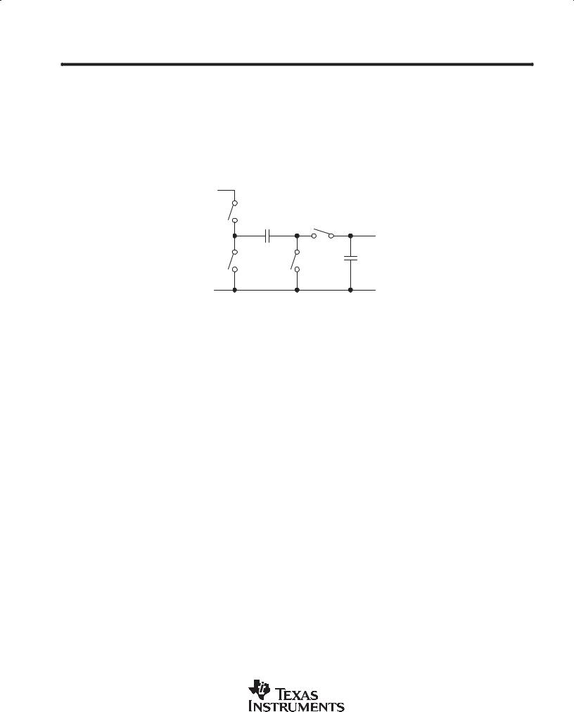
The TPS60400, TPS60401 charge pumps invert the voltage applied to their input. For the highest performance, use low equivalent series resistance (ESR) capacitors (e.g., ceramic). During the first half-cycle, switches S2
and S4 open, switches S1 and S3 close, and capacitor (C(fly)) charges to the voltage at VI. During the second half-cycle, S1 and S3 open, S2 and S4 close. This connects the positive terminal of C(fly) to GND and the negative to VO. By connecting C(fly) in parallel, CO is charged negative. The actual voltage at the output is more
positive than −V I, since switches S1–S4 have resistance and the load drains charge from CO.
VI |
|
|
|
|
S1 |
|
|
|
|
|
C(fly) |
|
S4 |
|
|
|
|
|
|
|
|
|
|
VO (−V I) |
|
1 F |
|
CO |
|
S2 |
|
S3 |
||
|
1 |
F |
||
|
|
|
||
GND |
|
|
|
GND |
Figure 1. Operating Principle
charge-pump output resistance
The TPS6040x devices are not voltage regulators. The charge pumps output source resistance is approximately 15 Ω at room temperature (with VI = 5 V), and VO approaches –5 V when lightly loaded. VO will droop toward GND as load current increases.
VO = −(V I – RO × IO)
1 |
(1) |
||
RO [ |
|
|
) 4 2RSWITCH ) ESRCFLY ) ESRCO |
ƒosc C |
|
||
|
|
(fly) |
|
RO = output resistance of the converter |
|||
efficiency considerations
The power efficiency of a switched-capacitor voltage converter is affected by three factors: the internal losses in the converter IC, the resistive losses of the capacitors, and the conversion losses during charge transfer between the capacitors. The internal losses are associated with the IC’s internal functions, such as driving the switches, oscillator, etc. These losses are affected by operating conditions such as input voltage, temperature, and frequency. The next two losses are associated with the voltage converter circuit’s output resistance. Switch losses occur because of the on-resistance of the MOSFET switches in the IC. Charge-pump capacitor losses occur because of their ESR. The relationship between these losses and the output resistance is as follows:
PCAPACITOR LOSSES + PCONVERSION LOSSES = IO2 × RO
RSWITCH = resistance of a single MOSFET-switch inside the converter fOSC = oscillator frequency
The first term is the effective resistance from an ideal switched-capacitor circuit. Conversion losses occur during the charge transfer between C(fly) and CO when there is a voltage difference between them. The power loss is:
1 |
2 |
2 |
) |
1 |
2 |
* 2VOVRIPPLE |
(2) |
PCONV.LOSS + 2 |
C(fly) VI |
* VO |
2 CO VRIPPLE |
ƒosc |
|||
|
|
|
|
|
|
|
|
WWW.TI.COM |
3 |

TPS60400, TPS60401, TPS60402, TPS60403
UNREGULATED 60 mA CHARGE PUMP VOLTAGE INVERTER
SLVS324A − JULY 2001 REVISED NOVEMBER 2004
efficiency considerations (continued)
The efficiency of the TPS6040x devices is dominated by their quiescent supply current at low output current and by their output impedance at higher current.
|
I |
1 * |
I |
O |
R |
O |
|
h ^ |
O |
|
|
||||
IO ) IQ |
|
VI |
|
|
Where, IQ = quiescent current.
capacitor selection
To maintain the lowest output resistance, use capacitors with low ESR (see Table 1). The charge-pump output
resistance is a function of C(fly)’s and CO’s ESR. Therefore, minimizing the charge-pump capacitor’s ESR minimizes the total output resistance. The capacitor values are closely linked to the required output current and
the output noise and ripple requirements. It is possible to only use 1- F capacitors of the same type.
input capacitor (CI)
Bypass the incoming supply to reduce its ac impedance and the impact of the TPS6040x switching noise. The recommended bypassing depends on the circuit configuration and where the load is connected. When the inverter is loaded from OUT to GND, current from the supply switches between 2 x IO and zero. Therefore, use a large bypass capacitor (e.g., equal to the value of C(fly)) if the supply has high ac impedance.
flying capacitor (C(fly))
Increasing the flying capacitor’s size reduces the output resistance. Small values increases the output resistance. Above a certain point, increasing C(fly)’s capacitance has a negligible effect, because the output resistance becomes dominated by the internal switch resistance and capacitor ESR.
output capacitor (CO)
Increasing the output capacitor’s size reduces the output ripple voltage. Decreasing its ESR reduces both output resistance and ripple. Smaller capacitance values can be used with light loads if higher output ripple can be tolerated. Use the following equation to calculate the peak-to-peak ripple.
VO(ripple) + |
IO |
|
|
|
|
|
|
|
||
|
) 2 |
IO |
ESRCO |
|
|
|
|
|||
fosc Co |
|
|
|
|
||||||
|
Table 1. Recommended Capacitor Values |
|
||||||||
|
|
|
|
|
|
|
|
|
|
|
|
DEVICE |
|
VI |
|
IO |
CI |
C(fly) |
|
CO |
|
|
|
[V] |
|
[mA] |
[ F] |
[ F] |
|
[ F] |
||
|
|
|
|
|
|
|||||
|
|
|
|
|
|
|
|
|
|
|
|
TPS60400 |
|
1.8…5.5 |
|
60 |
1 |
1 |
|
1 |
|
|
|
|
|
|
|
|
|
|
|
|
|
TPS60401 |
|
1.8…5.5 |
|
60 |
10 |
10 |
|
10 |
|
|
|
|
|
|
|
|
|
|
|
|
|
TPS60402 |
|
1.8…5.5 |
|
60 |
3.3 |
3.3 |
|
3.3 |
|
|
|
|
|
|
|
|
|
|
|
|
|
TPS60403 |
|
1.8…5.5 |
|
60 |
1 |
1 |
|
1 |
|
4 |
WWW.TI.COM |
TPS60400, TPS60401, TPS60402, TPS60403
UNREGULATED 60 mA CHARGE PUMP VOLTAGE INVERTER
SLVS324A − JULY 2001 REVISED NOVEMBER 2004
detailed description (continued)
Table 2. Recommended Capacitors
MANUFACTURER |
PART NUMBER |
SIZE |
CAPACITANCE |
TYPE |
|
|
|
|
|
|
|
Taiyo Yuden |
EMK212BJ474MG |
0805 |
0.47 |
F |
Ceramic |
|
LMK212BJ105KG |
0805 |
1 |
F |
Ceramic |
|
LMK212BJ225MG |
0805 |
2.2 |
F |
Ceramic |
|
EMK316BJ225KL |
1206 |
2.2 |
F |
Ceramic |
|
LMK316BJ475KL |
1206 |
4.7 |
F |
Ceramic |
|
JMK316BJ106KL |
1206 |
10 |
F |
Ceramic |
|
|
|
|
|
|
TDK |
C2012X5R1C105M |
0805 |
1 |
F |
Ceramic |
|
C2012X5R1A225M |
0805 |
2.2 |
F |
Ceramic |
|
C2012X5R1A335M |
0805 |
3.3 |
F |
Ceramic |
Table 3 contains a list of manufacturers of the recommended capacitors. Ceramic capacitors will provide the lowest output voltage ripple because they typically have the lowest ESR-rating.
Table 3. Recommended Capacitor Manufacturers
MANUFACTURER |
CAPACITOR TYPE |
INTERNET |
|
|
|
Taiyo Yuden |
X7R/X5R ceramic |
www.t-yuden.com |
|
|
|
TDK |
X7R/X5R ceramic |
www.component.tdk.com |
|
|
|
Vishay |
X7R/X5R ceramic |
www.vishay.com |
|
|
|
Kemet |
X7R/X5R ceramic |
www.kemet.com |
absolute maximum ratings over operating free-air temperature (unless otherwise noted)†
Voltage range: IN to GND . . . . . . . . . . . . . . . . . . . . . . . . . . . . . . . . . . . . . . . . . . . . |
. . . . . . . . . . . . −0.3 V to 5.5 |
V |
OUT to GND . . . . . . . . . . . . . . . . . . . . . . . . . . . . . . . . . . . . . . . . . . |
. . . . . . . . . . . . −5.5 V to 0.3 |
V |
CFLY− to GND . . . . . . . . . . . . . . . . . . . . . . . . . . . . . . . . . . . . . . . . . |
. . . . . . . 0.3 V to (VO − 0.3 V) |
|
CFLY+ to GND . . . . . . . . . . . . . . . . . . . . . . . . . . . . . . . . . . . . . . . . . |
. . . . . . −0.3 V to (V I + 0.3 |
V) |
Continuous power dissipation . . . . . . . . . . . . . . . . . . . . . . . . . . . . . . . . . . . . . . . . . . |
See Dissipation Rating Table |
|
Continuous output current . . . . . . . . . . . . . . . . . . . . . . . . . . . . . . . . . . . . . . . . . . . . . . |
. . . . . . . . . . . . . . . . . . . 80 mA |
|
Storage temperature range, Tstg . . . . . . . . . . . . . . . . . . . . . . . . . . . . . . . . . . . . . . . . . |
. . . . . . . . . . . −55 °C to 150°C |
|
Maximum junction temperature, TJ . . . . . . . . . . . . . . . . . . . . . . . . . . . . . . . . . . . . . . |
. . . . . . . . . . . . . . . . . . . 150°C |
|
†Stresses beyond those listed under “absolute maximum ratings” may cause permanent damage to the device. These are stress ratings only, and functional operation of the device at these or any other conditions beyond those indicated under “recommended operating conditions” is not implied. Exposure to absolute-maximum-rated conditions for extended periods may affect device reliability.
DISSIPATION RATING TABLE
PACKAGE |
TA < 25°C |
DERATING FACTOR |
TA = 70°C |
TA = 85°C |
|
POWER RATING |
ABOVE TA = 25°C |
POWER RATING |
POWER RATING |
||
|
|||||
DBV |
437 mW |
3.5 mW/°C |
280 mW |
227 mW |
WWW.TI.COM |
5 |
TPS60400, TPS60401, TPS60402, TPS60403
UNREGULATED 60 mA CHARGE PUMP VOLTAGE INVERTER
SLVS324A − JULY 2001 REVISED NOVEMBER 2004
recommended operating conditions
|
MIN |
NOM |
MAX |
UNIT |
|
|
|
|
|
Input voltage range, VI |
1.8 |
|
5.25 |
V |
Output current range at OUT, IO |
|
|
60 |
mA |
Input capacitor, CI |
0 |
C(fly) |
|
µF |
Flying capacitor, C(fly) |
|
1 |
|
µF |
Output capacitor, CO |
|
1 |
100 |
µF |
Operating junction temperature, TJ |
−40 |
|
125 |
°C |
electrical characteristics at CI = C(fly) = CO (according to Table 1), TC = −40 °C to 85°C, VI = 5 V over recommended operating free-air temperature range (unless otherwise noted)
|
PARAMETER |
|
TEST CONDITIONS |
MIN |
TYP |
MAX |
UNIT |
||
|
|
|
|
|
|
|
|
|
|
VI |
Supply voltage range |
|
At TC = −40 °C to 85°C, |
RL = 5 kΩ |
1.8 |
|
5.25 |
V |
|
|
At TC ≥ 0°C, |
|
RL = 5 kΩ |
1.6 |
|
|
|||
|
|
|
|
|
|
|
|||
IO |
Maximum output current at VO |
|
|
|
|
60 |
|
|
mA |
VO |
Output voltage |
|
|
|
|
|
−V I |
|
V |
|
|
TPS60400 |
|
C(fly) = 1 µF, CO = 2.2 µF |
|
35 |
|
|
|
VP−P |
Output voltage ripple |
TPS60401 |
IO = 5 mA |
C(fly) = CO = 10 µF |
|
20 |
|
mVP−P |
|
TPS60402 |
C(fly) = CO = 3.3 µF |
|
20 |
|
|||||
|
|
|
|
|
|
||||
|
|
TPS60403 |
|
C(fly) = CO = 1 µF |
|
15 |
|
|
|
|
|
TPS60400 |
|
|
|
|
125 |
270 |
|
|
|
|
|
|
|
|
|
|
|
|
|
TPS60401 |
At VI = 5 V |
|
|
|
65 |
190 |
µA |
|
|
|
|
|
|
|
|
||
|
|
TPS60402 |
|
|
|
120 |
270 |
||
|
|
|
|
|
|
|
|||
|
|
|
|
|
|
|
|
|
|
IQ |
Quiescent current (no-load input |
TPS60403 |
|
|
|
|
425 |
700 |
|
|
|
|
|
|
|
|
|
||
current) |
TPS60400 |
|
|
|
|
|
210 |
|
|
|
|
|
|
|
|
|
|
||
|
|
|
|
|
|
|
|
|
|
|
|
TPS60401 |
At T ≤ 60°C, |
VI = 5 V |
|
|
|
135 |
µA |
|
|
|
|
|
|
|
|||
|
|
TPS60402 |
|
|
|
210 |
|||
|
|
|
|
|
|
|
|
||
|
|
|
|
|
|
|
|
|
|
|
|
TPS60403 |
|
|
|
|
|
640 |
|
|
|
|
|
|
|
|
|
|
|
|
|
TPS60400 |
VCO version |
|
|
30 |
50−250 |
350 |
|
|
|
|
|
|
|
|
|
|
|
fOSC |
Internal switching frequency |
TPS60401 |
|
|
|
13 |
20 |
28 |
kHz |
|
|
|
|
|
|
|
|||
TPS60402 |
|
|
|
30 |
50 |
70 |
|||
|
|
|
|
|
|
||||
|
|
|
|
|
|
|
|
|
|
|
|
TPS60403 |
|
|
|
150 |
250 |
300 |
|
|
|
|
|
|
|
|
|
|
|
|
|
TPS60400 |
CI = C(fly) = CO = 1 µF |
|
|
12 |
15 |
|
|
|
Impedance at 25°C, VI = 5 V |
TPS60401 |
CI = C(fly) = CO = 10 µF |
|
|
12 |
15 |
Ω |
|
|
TPS60402 |
CI = C(fly) = CO = 3.3 µF |
|
|
12 |
15 |
|||
|
|
|
|
|
|||||
|
|
TPS60403 |
CI = C(fly) = CO = 1 µF |
|
|
12 |
15 |
|
|
6 |
WWW.TI.COM |
TPS60400, TPS60401, TPS60402, TPS60403
UNREGULATED 60 mA CHARGE PUMP VOLTAGE INVERTER
|
|
SLVS324A − JULY 2001 REVISED NOVEMBER 2004 |
|
||
|
|
|
|
|
|
|
|
TYPICAL CHARACTERISTICS |
|
|
|
|
|
Table of Graphs |
|
|
|
|
|
|
|
|
|
|
|
|
FIGURE |
|
|
|
|
|
|
|
|
η |
Efficiency |
vs Output current at 3.3 V, 5 V |
2, |
3 |
|
|
|
TPS60400, TPS60401, TPS60402, TPS60403 |
|
|
|
|
|
|
|
|
|
II |
Input current |
vs Output current |
4, |
5 |
|
|
|
TPS60400, TPS60401, TPS60402, TPS60403 |
|
|
|
|
|
|
|
|
|
IS |
Supply current |
vs Input voltage |
6, |
7 |
|
|
|
TPS60400, TPS60401, TPS60402, TPS60403 |
|
|
|
|
|
|
|
|
|
|
Output resistance |
vs Input voltage at −40 °C, 0°C, 25°C, 85°C |
8, 9, 10, |
|
|
|
|
TPS60400, CI = C(fly) = CO = 1 µF |
11 |
|
|
|
|
TPS60401, CI = C(fly) = CO = 10 µF |
|
|
|
|
|
TPS60402 , CI = C(fly) = CO = 3.3 µF |
|
|
|
|
|
TPS60403, CI = C(fly) = CO = 1 µF |
|
|
|
VO |
Output voltage |
vs Output current at 25°C, VIN=1.8 V, 2.5 V, 3.3 V, 5 V |
12, 13, |
|
|
|
|
TPS60400, CI = C(fly) = CO = 1 µF |
14, |
15 |
|
|
|
TPS60401, CI = C(fly) = CO = 10 µF |
|
|
|
|
|
TPS60402 , CI = C(fly) = CO = 3.3 µF |
|
|
|
|
|
TPS60403, CI = C(fly) = CO = 1 µF |
|
|
|
fOSC |
Oscillator frequency |
vs Temperature at VI = 1.8 V, 2.5 V, 3.3 V, 5 V |
16, 17, |
|
|
|
|
TPS60400, TPS60401, TPS60402, TPS60403 |
18, |
19 |
|
|
|
|
|
|
|
fOSC |
Oscillator frequency |
vs Output current TPS60400 at 2 V, 3.3 V, 5.0 V |
20 |
|
|
|
Output ripple and noise |
VI = 5 V, IO = 30 mA, CI = C(fly) = CO = 1 µF (TPS60400) |
21, |
22 |
|
|
|
VI = 5 V, IO = 30 mA, CI = C(fly) = CO = 10 µF (TPS60401) |
|
|
|
|
|
VI = 5 V, IO = 30 mA, CI = C(fly) = CO = 3.3 µF (TPS60402) |
|
|
|
|
|
VI = 5 V, IO = 30 mA, CI = C(fly) = CO = 1 µF (TPS60403) |
|
|
|
TPS60400, TPS60401 |
TPS60402, TPS60403 |
EFFICIENCY |
EFFICIENCY |
vs |
vs |
OUTPUT CURRENT |
OUTPUT CURRENT |
|
100 |
|
|
|
|
|
|
|
|
|
|
100 |
|
|
|
|
|
|
TPS60400 |
|
|
|
|
|
|
|
95 |
|
|
|
|
VI = 5 V |
|
TPS60401 |
|
95 |
||
|
|
|
|
|
|
|
|
|
|
|
||
|
90 |
|
|
|
|
|
|
|
VI = 5 V |
|
90 |
|
|
|
|
|
|
|
|
|
|
|
|
||
− % |
85 |
|
TPS60401 |
|
|
|
|
|
− % |
85 |
||
|
|
|
|
|
|
|
|
|||||
Efficiency |
80 |
|
VI = 3.3 V |
|
|
|
|
|
|
Efficiency |
80 |
|
|
|
|
|
|
|
|
|
|
||||
75 |
|
|
|
|
|
|
|
|
|
75 |
||
|
70 |
|
|
|
|
|
TPS60400 |
|
|
70 |
||
|
|
|
|
|
|
VI = 3.3 V |
|
|
||||
|
65 |
|
|
|
|
|
|
|
|
|
|
65 |
|
|
|
|
|
|
|
|
TA = 25°C |
|
|
||
|
60 |
10 |
20 |
30 |
40 |
50 |
60 |
70 |
80 |
90 |
100 |
60 |
|
0 |
|
||||||||||
|
|
|
|
IO − Output Current − mA |
|
|
|
|||||
|
|
|
|
|
TPS60403 |
|
|
|
|
|
|
|
|
|
|
VI = 5 V |
|
|
|
|
|
|
|
|
|
|
|
|
|
TPS60402 |
|
|
|
|
|
|
|
|
|
|
VI = 5 V |
|
|
|
|
|
|
TPS60403 |
|
|
|
|
|
|
|
|
|
|
VI = 3.3 V |
|
|
|
|
|
|
|
|
|
|
|
|
TPS60402 |
|
|
||
|
|
|
|
|
|
VI = 3.3 V |
|
|
||
|
|
|
|
|
|
|
TA = 25°C |
|
||
0 |
10 |
20 |
30 |
40 |
50 |
60 |
70 |
80 |
90 |
100 |
|
|
|
IO − Output Current − mA |
|
|
|
||||
Figure 2 |
Figure 3 |
|
|
|
|
WWW.TI.COM |
7 |

TPS60400, TPS60401, TPS60402, TPS60403
UNREGULATED 60 mA CHARGE PUMP VOLTAGE INVERTER
SLVS324A − JULY 2001 REVISED NOVEMBER 2004
TYPICAL CHARACTERISTICS
TPS60400, TPS60401 |
TPS60402, TPS60403 |
INPUT CURRENT |
INPUT CURRENT |
vs |
vs |
OUTPUT CURRENT |
OUTPUT CURRENT |
|
100 |
TA = 25°C |
|
|
100 |
TA = 25°C |
|
|
|
|
|
|
|
|
|
||
|
|
|
TPS60400 |
|
|
|
|
|
mA− |
|
|
VI = 5 V |
mA− |
|
VI |
= 5 V |
|
|
10 |
|
|
|
10 |
TPS60403 |
|
|
Current |
|
TPS60401 |
|
Current |
|
TPS60403 |
|
|
Input− |
1 |
VI = 5 V |
VI = 2 V |
Input− |
1 |
VI = 2 V |
|
|
|
|
|
TPS60401 |
|
|
|
|
|
I |
|
|
|
I |
|
|
TPS60402 |
|
I |
|
|
|
I |
|
|
|
|
|
|
|
|
|
|
|
VI = 5 V |
|
|
|
TPS60400 |
|
|
|
TPS60402 |
|
|
|
0.1 |
VI = 2 V |
|
|
|
VI = 2 V |
|
|
|
|
|
|
0.1 |
|
|
|
|
|
0.1 |
1 |
10 |
100 |
0.1 |
1 |
10 |
100 |
|
|
IO − Output Current − mA |
|
|
IO − Output Current − mA |
|
||
Figure 4 |
Figure 5 |
TPS60400, TPS60401 |
TPS60402, TPS60403 |
SUPPLY CURRENT |
SUPPLY CURRENT |
vs |
vs |
INPUT VOLTAGE |
INPUT VOLTAGE |
|
0.6 |
|
|
|
|
|
0.6 |
|
|
|
|
|
|
|
|
|
|
IO = 0 mA |
|
|
|
|
|
IO = 0 mA |
|
|
|
|
|
|
TA = 25°C |
|
|
|
|
|
TA = 25°C |
|
−mA |
0.4 |
|
|
|
|
|
−mA |
|
|
|
|
|
CurrentSupply− |
|
|
|
|
|
0.4 |
|
|
|
|
|
|
0.2 |
|
|
|
|
|
CurrentSupply− |
|
|
TPS60403 |
|
||
|
|
|
|
|
|
|
|
|
|
|
||
DD |
|
|
|
|
|
|
0.2 |
|
|
|
|
|
|
|
|
|
|
|
DD |
|
|
|
|
|
|
I |
|
|
|
TPS60400 |
|
|
I |
|
|
|
|
|
|
|
|
|
|
|
|
|
|
|
|
|
|
|
|
|
|
|
TPS60401 |
|
|
|
|
|
TPS60402 |
|
|
0 |
|
|
|
|
0 |
|
|
|
|
|
|
|
|
|
|
|
|
|
|
|
|
|
||
|
0 |
1 |
2 |
3 |
4 |
5 |
0 |
1 |
2 |
3 |
4 |
5 |
|
|
|
VI − Input Voltage − V |
|
|
|
|
VI − Input Voltage − V |
|
|
||
Figure 6 |
Figure 7 |
|
|
|
|
8 |
WWW.TI.COM |
TPS60400, TPS60401, TPS60402, TPS60403
UNREGULATED 60 mA CHARGE PUMP VOLTAGE INVERTER
|
SLVS324A − JULY 2001 REVISED NOVEMBER 2004 |
|
|
TYPICAL CHARACTERISTICS |
|
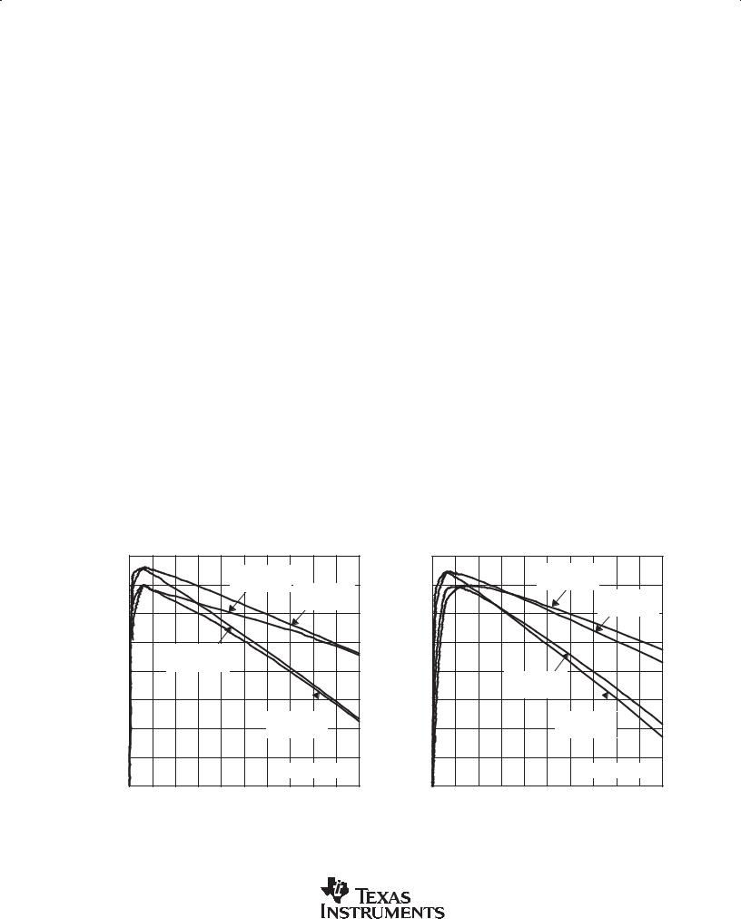
TPS60400 |
TPS60401 |
OUTPUT RESISTANCE |
OUTPUT RESISTANCE |
vs |
vs |
INPUT VOLTAGE |
INPUT VOLTAGE |
|
40 |
|
|
|
|
|
|
40 |
|
|
|
|
|
|
|
|
|
|
|
|
|
IO = 30 mA |
|
|
|
||
|
|
|
|
IO = 30 mA |
|
|
|
|
|
|
|
||
|
35 |
|
|
CI = C(fly) = CO = 1 F |
|
|
35 |
CI = C(fly) = CO = 10 F |
|
|
|||
Ω |
30 |
|
|
|
|
|
|
30 |
|
|
|
|
|
|
|
|
|
|
|
Resistance− Ω |
|
|
|
|
|
||
ResistanceOutput− |
|
|
|
|
|
|
|
|
|
|
|
||
25 |
|
|
|
|
|
25 |
|
|
|
|
|
||
|
|
|
|
|
|
|
|
|
|
|
|
||
|
|
|
|
|
|
|
|
|
|
|
|
|
|
|
20 |
|
TA = 85°C |
|
|
|
|
20 |
|
TA = 25°C |
|
|
|
|
|
|
TA = 25°C |
|
|
|
15 |
|
TA = 85°C |
|
|
||
r |
15 |
|
|
|
Output |
|
|
|
|
||||
|
|
|
|
|
|
|
|
|
|
|
|||
|
|
|
|
|
|
|
|
|
|
|
|
|
|
− |
|
|
|
|
|
|
|
|
|
|
|
|
|
o |
10 |
|
|
|
|
|
|
10 |
|
|
|
|
|
|
|
|
|
|
|
− |
|
|
|
|
|
||
|
|
|
|
|
|
o |
|
|
|
|
|
|
|
|
|
|
|
|
|
|
|
|
|
|
|
|
|
|
|
|
|
|
|
|
r |
|
|
|
|
|
|
|
5 |
|
|
|
|
|
|
5 |
|
|
|
|
|
|
|
TA = −40 °C |
|
|
|
|
TA = −40 °C |
|
|
|
|||
|
|
|
|
|
|
0 |
|
|
|
||||
|
0 |
|
|
|
|
|
|
|
|
|
|
|
|
|
1 |
2 |
3 |
4 |
5 |
6 |
|
1 |
2 |
3 |
4 |
5 |
6 |
|
|
|
VI − Input Voltage − V |
|
|
|
|
|
VI − Input Voltage − V |
|
|
||
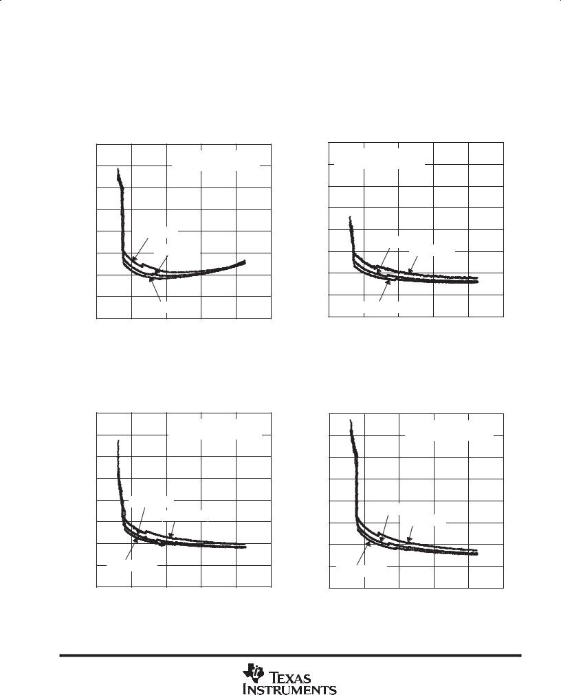
Figure 8 |
Figure 9 |
|
|
|
TPS60402 |
|
|
|
|
TPS60403 |
|
|
|||
|
|
|
OUTPUT RESISTANCE |
|
|
|
|
OUTPUT RESISTANCE |
|
|
|||
|
|
|
|
vs |
|
|
|
|
vs |
|
|
||
|
|
|
INPUT VOLTAGE |
|
|
|
|
INPUT VOLTAGE |
|
|
|||
|
40 |
|
|
|
|
|
40 |
|
|
|
|
|
|
|
|
|
|
IO = 30 mA |
|
|
|
|
I |
O |
= 30 mA |
|
|
|
35 |
|
|
CI = C(fly) = CO = 3.3 F |
|
35 |
|
CI = C(fly) = CO = 1 |
F |
||||
Ω |
|
|
|
|
|
|
|
|
|
|
|
|
|
− |
30 |
|
|
|
|
Ω |
30 |
|
|
|
|
|
|
ResistanceOutput |
25 |
|
|
|
|
Resistance− |
25 |
|
|
|
|
|
|
|
|
|
|
|
|
|
|
|
|
|
|
||
|
20 |
TA = 25°C |
|
|
|
20 |
|
TA = 25°C |
|
|
|
|
|
|
|
|
TA = 85°C |
|
Output |
|
|
|
|
|
|
||
o |
15 |
|
|
15 |
|
TA = 85°C |
|
|
|||||
|
|
|
|
|
|
|
|||||||
|
|
|
|
|
|
|
|
|
|||||
− |
|
|
|
|
|
|
|
|
|
|
|
|
|
r |
10 |
|
|
|
|
− |
10 |
|
|
|
|
|
|
|
|
|
|
|
r |
|
|
|
|
|
|
||
|
|
|
|
|
|
o |
|
|
|
|
|
|
|
|
5 |
TA = −40 °C |
|
|
|
5 |
TA = −40 |
°C |
|
|
|
|
|
|
|
|
|
|
|
|
|
|
|
|
|
||
|
0 |
|
|
|
|
|
0 |
|
|
|
|
|
|
|
1 |
2 |
3 |
4 |
5 |
6 |
1 |
2 |
3 |
|
4 |
5 |
6 |
|
|
|
VI − Input Voltage − V |
|
|
|
|
VI − Input Voltage − V |
|
|
|||
|
|
|
Figure 10 |
|
|
|
|
Figure 11 |
|
|
|||
|
|
|
|
|
|
WWW.TI.COM |
|
|
|
|
|
|
9 |
 Loading...