


TMS320LC546APZ-66
Texas Instruments TMS320LC546APZ-66, TMS320LC546APZ-50, TMS320LC545APBK-66, TMS320LC545APBK-50, TMS320LC543PZ2-50 Datasheet
...
TMS320C54x, TMS320LC54x, TMS320VC54x
FIXED-POINT DIGITAL SIGNAL PROCESSORS
SPRS039C – FEBRUARY 1996 – REVISED DECEMBER 1999
1
POST OFFICE BOX 1443 • HOUSTON, TEXAS 77251–1443
D Advanced Multibus Architecture With Three
Separate 16-Bit Data Memory Buses and
One Program Memory Bus
D 40-Bit Arithmetic Logic Unit (ALU)
Including a 40-Bit Barrel Shifter and Two
Independent 40-Bit Accumulators
D 17- × 17-Bit Parallel Multiplier Coupled to a
40-Bit Dedicated Adder for Non-Pipelined
Single-Cycle Multiply/Accumulate (MAC)
Operation
D Compare, Select, and Store Unit (CSSU) for
the Add/Compare Selection of the Viterbi
Operator
D Exponent Encoder to Compute an
Exponent Value of a 40-Bit Accumulator
Value in a Single Cycle
D T wo Address Generators With Eight
Auxiliary Registers and Two Auxiliary
Register Arithmetic Units (ARAUs)
D Data Bus With a Bus Holder Feature
D Address Bus With a Bus Holder Feature
(’548 and ’549 Only)
D Extended Addressing Mode for 8M × 16-Bit
Maximum Addressable External Program
Space (’548 and ’549 Only)
D 192K × 16-Bit Maximum Addressable
Memory Space (64K Words Program,
64K Words Data, and 64K Words I/O)
D On-Chip ROM with Some Configurable to
Program/Data Memory
D Dual-Access On-Chip RAM
D Single-Access On-Chip RAM (’548/’549)
D Single-Instruction Repeat and
Block-Repeat Operations for Program Code
D Block-Memory-Move Instructions for Better
Program and Data Management
D Instructions With a 32-Bit Long Word
Operand
D Instructions With Two- or Three-Operand
Reads
D Arithmetic Instructions With Parallel Store
and Parallel Load
D Conditional Store Instructions
D Fast Return From Interrupt
D On-Chip Peripherals
– Software-Programmable Wait-State
Generator and Programmable Bank
Switching
– On-Chip Phase-Locked Loop (PLL) Clock
Generator With Internal Oscillator or
External Clock Source
– Full-Duplex Serial Port to Support 8- or
16-Bit Transfers (’541, ’LC545, and
’LC546 Only)
– Time-Division Multiplexed (TDM) Serial
Port (’542, ’543, ’548, and ’549 Only)
– Buffered Serial Port (BSP) (’542, ’543,
’LC545, ’LC546, ’548, and ’549 Only)
– 8-Bit Parallel Host-Port Interface (HPI)
(’542, ’LC545, ’548, and ’549)
– One 16-Bit Timer
– External-Input/Output (XIO) Off Control
to Disable the External Data Bus,
Address Bus and Control Signals
D Power Consumption Control With IDLE1,
IDLE2, and IDLE3 Instructions With
Power-Down Modes
D CLKOUT Off Control to Disable CLKOUT
D On-Chip Scan-Based Emulation Logic,
IEEE Std 1149.1
†
(JTAG) Boundary Scan
Logic
D 25-ns Single-Cycle Fixed-Point Instruction
Execution Time [40 MIPS] for 5-V Power
Supply (’C541 and ’C542 Only)
D 20-ns and 25-ns Single-Cycle Fixed-Point
Instruction Execution Time (50 MIPS and
40 MIPS) for 3.3-V Power Supply (’LC54x)
D 15-ns Single-Cycle Fixed-Point Instruction
Execution Time (66 MIPS) for 3.3-V Power
Supply (’LC54xA, ’548, ’LC549)
D 12.5-ns Single-Cycle Fixed-Point
Instruction Execution Time (80 MIPS) for
3.3-V Power Supply (’LC548, ’LC549)
D 10-ns and 8.3-ns Single-Cycle Fixed-Point
Instruction Execution Time (100 and 120
MIPS) for 3.3-V Power Supply (2.5-V Core)
(’VC549)
Please be aware that an important notice concerning availability, standard warranty, and use in critical applications of
Texas Instruments semiconductor products and disclaimers thereto appears at the end of this data sheet.
Copyright 1999, Texas Instruments Incorporated
†
IEEE Standard 1149.1-1990 Standard-Test-Access Port and Boundary Scan Architecture.
PRODUCTION DATA information is current as of publication date.
Products conform to specifications per the terms of Texas Instruments
standard warranty. Production processing does not necessarily include
testing of all parameters.

TMS320C54x, TMS320LC54x, TMS320VC54x
FIXED-POINT DIGITAL SIGNAL PROCESSORS
SPRS039C – FEBRUARY 1996 – REVISED DECEMBER 1999
2
POST OFFICE BOX 1443 • HOUSTON, TEXAS 77251–1443
description
The TMS320C54x, TMS320LC54x, and TMS320VC54x fixed-point, digital signal processor (DSP) families
(hereafter referred to as the ’54x unless otherwise specified) are based on an advanced modified Harvard
architecture that has one program memory bus and three data memory buses. These processors also provide
an arithmetic logic unit (ALU) that has a high degree of parallelism, application-specific hardware logic, on-chip
memory , and additional on-chip peripherals. These DSP families also provide a highly specialized instruction
set, which is the basis of the operational flexibility and speed of these DSPs.
Separate program and data spaces allow simultaneous access to program instructions and data, providing the
high degree of parallelism. Two reads and one write operation can be performed in a single cycle. Instructions
with parallel store and application-specific instructions can fully utilize this architecture. In addition, data can be
transferred between data and program spaces. Such parallelism supports a powerful set of arithmetic, logic,
and bit-manipulation operations that can all be performed in a single machine cycle. In addition, the ’C54x,
’LC54x, and ’VC54x versions include the control mechanisms to manage interrupts, repeated operations, and
function calls.
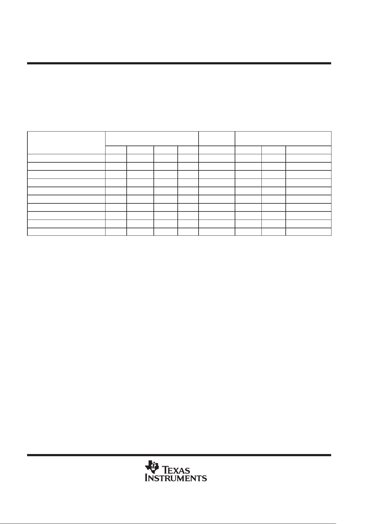
Table 1 provides an overview of the ’54x generation of DSPs. The table shows significant features of each
device including the capacity of on-chip RAM and ROM memories, the peripherals, the execution time of one
machine cycle, and the type of package with its total pin count.
Table 1. Characteristics of the ’54x Processors
NOMINAL
ON-CHIP
MEMORY
PERIPHERALS
CYCLE
DSP TYPE
NOMINAL
VOLTAGE (V)
RAM
†
(Word)
ROM
(Word)
SERIAL
PORT
TIMER HPI
CYCLE
TIME (ns)
PACKAGE TYPE
TMS320C541 5.0 5K 28K
‡
2
§
1 No 25 100-pin TQFP
TMS320LC541 3.3 5K 28K
‡
2
§
1 No 20/25 100-pin TQFP
TMS320LC541Bh 3.3 5K 28K
‡
2
§
1 No 20/25 100-pin TQFP
TMS320C542 5.0 10K 2K 2
¶
1 Yes 25 144-pin TQFP
TMS320LC542 3.3 10K 2K 2
¶
1 Yes 20/25 128-pin TQFP/144-pin TQFP
TMS320LC543 3.3 10K 2K 2
¶
1 No 20/25 100-pin TQFP
TMS320LC545 3.3 6K 48K
#
2
||
1 Yes 20/25 128-pin TQFP
TMS320LC545Ah 3.3 6K 48K
#
2
||
1 Yes 15/20/25 128-pin TQFP
TMS320LC545Bh 3.3 6K 48K
#
2
||
1 Yes 15/20/25 128-pin TQFP
TMS320LC546 3.3 6K 48K
#
2
||
1 No 20/25 100-pin TQFP
TMS320LC546Ah 3.3 6K 48K
#
2
||
1 No 15/20/25 100-pin TQFP
TMS320LC546Bh 3.3 6K 48K
#
2
||
1 No 15/20/25 100-pin TQFP
TMS320LC548h 3.3 32K 2K 3k 1 Yes 12.5/15/20 144-pin TQFP/144-pin BGA
TMS320LC549h 3.3 32K 16K 3k 1 Yes 12.5/15 144-pin TQFP/144-pin BGA
TMS320VC549h 3.3 (2.5 core) 32K 16K 3k 1 Yes 8.3/10/12.5 144-pin TQFP/144-pin BGA
Legend:
TQFP = Thin Quad Flatpack
BGA = MicroStar BGA (Ball Grid Array)
†
The dual-access RAM (single access RAM on ’548 and ’549 devices) can be configured as data memory or program/data memory.
‡
For ’C541/’LC541, 8K words of ROM can be configured as program memory or program/data memory.
§
Two standard (general-purpose) serial ports
¶
One TDM and one BSP
#
For ’LC545/’LC546, 16K words of ROM can be configured as program memory or program/data memory.
||
One standard and one BSP
kOne TDM and two BSPs
hRefer to separate data sheet for electrical specifications.
MicroStar BGA is a trademark of Texas Instruments Incorporated.

TMS320C54x, TMS320LC54x, TMS320VC54x
FIXED-POINT DIGITAL SIGNAL PROCESSORS
SPRS039C – FEBRUARY 1996 – REVISED DECEMBER 1999
3
POST OFFICE BOX 1443 • HOUSTON, TEXAS 77251–1443
CLKR0
V
SS
A10
A11
A12
A13
A14
A15
CV
DD
V
SS
CV
DD
READY
PS
DS
IS
R/W
MSTRB
IOSTRB
MSC
XF
HOLDA
HOLD
BIO
MP/MC
1
2
3
4
5
6
7
8
9
10
11
12
13
14
15
16
17
18
19
20
21
22
23
24
25
76
77
78
79
80
81
82
83
84
85
86
87
88
89
90
91
92
93
94
95
96
97
98
99
100
75
74
73
72
71
70
69
68
67
66
65
64
63
62
61
60
59
58
57
56
55
54
53
52
51
50
49
48
47
46
45
44
43
42
41
40
39
38
37
36
35
34
33
32
31
30
29
28
27
26
A5
A4
A3
A2
A1
V
V
D14
D13
D12
D11
D10
D9
D8
D7
D6
DV
SS
CLKR1
FSR0
FSR1
DR0
DR1
CLKX1
DD
FSX1
DD
SS
INT1
INT3
SS
V
SS
A6
D15
INT2
TMS320C541, TMS320LC541
PZ PACKAGE
†
(TOP VIEW)
IAQ
A0
CLKX0
NMI
D5
D4
D3
D2
D1
D0
RS
X2/CLKIN
X1
V
SS
CV
DD
V
SS
TMS
TCK
TRST
TDI
TDO
EMU1/OFF
EMU0
TOUT
CLKMD3
CLKMD2
CLKMD1
CLKOUT
CNT
A9
A8
A7
SS
SS
DD
V
DV
V
V
CV
SS
V
FSX0
DX0
DX1
IACK
DD
CV
INT0
CV
DD
DV
DD
†
DV
DD
is the power supply for the I/O pins while CV
DD
is the power supply for the core CPU, and V
SS
is the ground for both the I/O pins and the
core CPU.
The ’54x signal descriptions table lists each terminal name, function, and operating mode(s) for the
TMS320C541PZ/TMS320LC541PZ (100-pin TQFP packages).
For the ’C541/’LC541 (100-pin packages), no letter in front of CLKRn, FSRn, DRn, CLKXn, FSXn, and DXn pin
names denotes standard serial port (where n = 0 or 1 port).
TMS320C54x, TMS320LC54x, TMS320VC54x
FIXED-POINT DIGITAL SIGNAL PROCESSORS
SPRS039C – FEBRUARY 1996 – REVISED DECEMBER 1999
4
POST OFFICE BOX 1443 • HOUSTON, TEXAS 77251–1443
CV
HDS1
V
SS
NC
V
SS
DV
DD
D5
D4
D3
D2
D1
D0
RS
X2/CLKIN
X1
HD3
CLKOUT
V
SS
HPIENA
CV
DD
V
SS
TMS
TCK
TRST
TDI
TDO
EMU1/OFF
EMU0
TOUT
HD2
CNT
CLKMD3
CLKMD2
CLKMD1
V
SS
DV
DD
NC
V
SS
V
SS
NC
V
SS
DV
DD
A10
HD7
A11
A12
A13
A14
A15
CV
DD
HAS
V
SS
V
SS
CV
DD
HCS
HR/W
READY
PS
DS
IS
R/W
MSTRB
IOSTRB
MSC
XF
HOLDA
IAQ
HOLD
BIO
MP/MC
DV
DD
V
SS
NC
V
SS
SS
V
144
NC
CV
143
142
141
A8
140
A7
139
A6
138
A5
137
A4
136
HD6
135
A3
134
A2
133
A1
132
A0
131
DV
130
129
128
127
V
126
125
HD5
124
D15
123
D14
122
D13
121
HD4
120
D12
119
D11
118
117
D9
116
D8
115
D7
114
D6
113
112
37
38
39
40
41
42
43
44
45
46
47
48
49
50
51
52
53
54
55
56
57
58
59
60
61
62
63
64
65
66
67
68
69
1
2
3
4
5
6
7
8
9
10
11
12
13
14
15
16
17
18
19
20
21
22
23
24
25
26
27
28
29
30
31
32
33
34
35
36
108
107
106
105
104
103
102
101
100
99
98
97
96
95
94
93
92
91
90
89
88
87
86
85
84
83
82
81
80
79
78
77
76
75
74
73
SS
V
NC
HCNTL0
SS
BCLKR
TCLKR
BFSR
TFSR/TADD
BDR
HCNTL1
TDR
BCLKX
TCLKX
SS
DD
SS
HD0
BDX
TDX
IACK
HBIL
NMI
INT0
INT1
INT2
INT3
DD
HD1
SS
HRDY
HINT
111
V
110
V
109
70
71
72
NC
SS
V
D10
TFSX/TFRM
SS
NC
DV
DD
CV
HDS2
SS
V
V
V
DV
V
CV
V
DD
DD
DD
DD
SS
SS
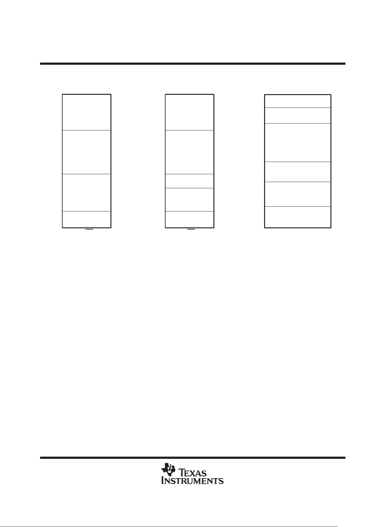
TMS320C542/TMS320LC542
PGE PACKAGE
†‡
(TOP VIEW)
BFSX
A9
†
NC = No connection
‡
DV
DD
is the power supply for the I/O pins while CV
DD
is the power supply for the core CPU, and V
SS
is the ground for both the I/O pins and the
core CPU.
The ’54x signal descriptions table lists each terminal name, function, and operating mode(s) for the
TMS320C542PGE/’LC542PGE (144-pin TQFP packages).
For the ’C542/’LC542 (144-pin TQFP packages), the letter B in front of CLKR, FSR, DR, CLKX, FSX, and DX
pin names denotes buffered serial port (BSP). The letter T in front of CLKR, FSR, DR, CLKX, FSX, and DX pin
names denotes time-division multiplexed (TDM) serial port.

TMS320C54x, TMS320LC54x, TMS320VC54x
FIXED-POINT DIGITAL SIGNAL PROCESSORS
SPRS039C – FEBRUARY 1996 – REVISED DECEMBER 1999
5
POST OFFICE BOX 1443 • HOUSTON, TEXAS 77251–1443
V
SS
DV
DD
A10
HD7
A11
A12
A13
A14
A15
CV
DD
HAS
V
SS
V
SS
CV
DD
HCS
HR/W
READY
PS
DS
IS
R/W
MSTRB
IOSTRB
MSC
XF
HOLDA
IAQ
HOLD
BIO
MP/MC
DV
DD
V
SS
V
SS
DV
DD
D5
D4
D3
D2
D1
D0
RS
X2/CLKIN
X1
HD3
CLKOUT
V
SS
HPIENA
CV
DD
V
SS
TMS
TCK
TRST
TDI
TDO
EMU1/OFF
EMU0
TOUT
HD2
CNT
CLKMD3
CLKMD2
CLKMD1
V
SS
DV
DD
96
95
94
93
92
91
90
89
88
87
86
85
84
83
82
81
80
79
78
77
76
75
74
73
72
71
70
69
68
67
66
65
1
2
3
4
5
6
7
8
9
10
11
12
13
14
15
16
17
18
19
20
21
22
23
24
25
26
27
28
29
30
31
32
128
33
127126125124123122121 120119118117116115114113112 111110109108107106105104103102101100 99 98 97
34 35 36 37 38 39 40 41 42 43 44 45 46 47 48 49 50 51 52 53 54 55 56 57 58 59 60 61 62 63 64
HCNTL0 CV
SS
A9
BCLKR A8
TCLKR A7
BFSR A6
TFSR/TADD A5
BDR A4
HCNTL1 HD6
TDR A3
BCLKX A2
TCLKX A1
SS
A0
HINT
DV
DD
HDS2
BFSX
V
TFSX/TFRM
HDS1
HRDY V
DD
CV
SS
HD5
HD0 D15
BDX D14
TDX D13
IACK HD4
HBIL D12
NMI D11
INT0 D10
INT1 D9
INT2 D8
INT3 D7
DD
D6
HD1
DV
SS
V
DD
DD
V
CV
V
CV
DV
V
V
SS
DD
DD
SS
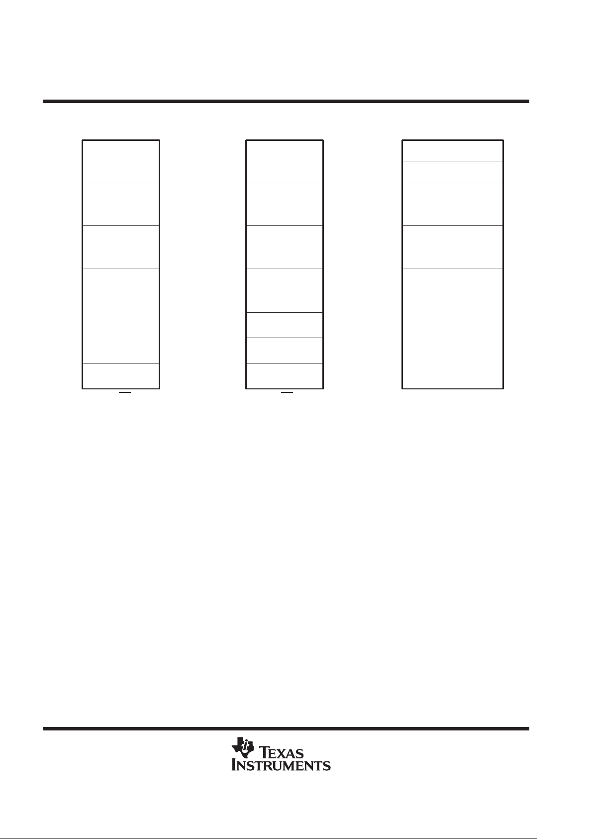
TMS320LC542
PBK PACKAGE
†
(TOP VIEW)
SS
†
DV
DD
is the power supply for the I/O pins while CV
DD
is the power supply for the core CPU, and V
SS
is the ground for both the I/O pins and the
core CPU.
The ’54x signal descriptions table lists each terminal name, function, and operating mode(s) for the
TMS320LC542PBK (128-pin TQFP package).
For the ’LC542 (128-pin TQFP package), the letter B in front of CLKR, FSR, DR, CLKX, FSX, and DX pin names
denotes buffered serial port (BSP). The letter T in front of CLKR, FSR, DR, CLKX, FSX, and DX pin names
denotes time-division multiplexed (TDM) serial port.

TMS320C54x, TMS320LC54x, TMS320VC54x
FIXED-POINT DIGITAL SIGNAL PROCESSORS
SPRS039C – FEBRUARY 1996 – REVISED DECEMBER 1999
6
POST OFFICE BOX 1443 • HOUSTON, TEXAS 77251–1443
BCLKR
V
SS
A10
A11
A12
A13
A14
A15
CV
DD
V
SS
CV
DD
READY
PS
DS
IS
R/W
MSTRB
IOSTRB
MSC
XF
HOLDA
HOLD
BIO
MP/MC
1
2
3
4
5
6
7
8
9
10
11
12
13
14
15
16
17
18
19
20
21
22
23
24
25
76
77
78
79
80
81
82
83
84
85
86
87
88
89
90
91
92
93
94
95
96
97
98
99
100
75
74
73
72
71
70
69
68
67
66
65
64
63
62
61
60
59
58
57
56
55
54
53
52
51
50
49
48
47
46
45
44
43
42
41
40
39
38
37
36
35
34
33
32
31
30
29
28
27
26
A5
A4
A3
A2
A1
V
V
D14
D13
D12
D11
D10
D9
D8
D7
D6
DV
SS
TCLKR
BFSR
TFSR
BDR
TDR
TCLKX
DD
TFSX
DD
SS
INT1
INT3
SS
V
SS
A6
D15
INT2
TMS320LC543
PZ PACKAGE
†
(TOP VIEW)
IAQ
A0
BCLKX
NMI
D5
D4
D3
D2
D1
D0
RS
X2/CLKIN
X1
V
SS
CV
DD
V
SS
TMS
TCK
TRST
TDI
TDO
EMU1/OFF
EMU0
TOUT
CLKMD3
CLKMD2
CLKMD1
CLKOUT
CNT
A9
A8
A7
SS
SS
DD
V
DV
V
V
CV
SS
V
BFSX
BDX
TDX
IACK
DD
CV
INT0
CV
DD
DV
DD
†
DV
DD
is the power supply for the I/O pins while CV
DD
is the power supply for the core CPU, and V
SS
is the ground for both the I/O pins and the
core CPU.
The ’54x signal descriptions table lists each terminal name, function, and operating mode(s) for the
TMS320LC543PZ (100-pin TQFP package).
For the ’LC543 (100-pin TQFP package), the letter B in front of CLKR, FSR, DR, CLKX, FSX, and DX denotes
buffered serial port (BSP). The letter T in front of CLKR, FSR, DR, CLKX, FSX, and DX denotes time-division
multiplexed (TDM) serial port.

TMS320C54x, TMS320LC54x, TMS320VC54x
FIXED-POINT DIGITAL SIGNAL PROCESSORS
SPRS039C – FEBRUARY 1996 – REVISED DECEMBER 1999
7
POST OFFICE BOX 1443 • HOUSTON, TEXAS 77251–1443
V
SS
DV
DD
A10
HD7
A11
A12
A13
A14
A15
CV
DD
HAS
V
SS
V
SS
CV
DD
HCS
HR/W
READY
PS
DS
IS
R/W
MSTRB
IOSTRB
MSC
XF
HOLDA
IAQ
HOLD
BIO
MP/MC
DV
DD
V
SS
V
SS
DV
DD
D5
D4
D3
D2
D1
D0
RS
X2/CLKIN
X1
HD3
CLKOUT
V
SS
HPIENA
CV
DD
V
SS
TMS
TCK
TRST
TDI
TDO
EMU1/OFF
EMU0
TOUT
HD2
CNT
CLKMD3
CLKMD2
CLKMD1
V
SS
DV
DD
96
95
94
93
92
91
90
89
88
87
86
85
84
83
82
81
80
79
78
77
76
75
74
73
72
71
70
69
68
67
66
65
1
2
3
4
5
6
7
8
9
10
11
12
13
14
15
16
17
18
19
20
21
22
23
24
25
26
27
28
29
30
31
32
128
33
127126125124123122121 120119118117116115114113112 111110109108107106105104103102101100 99 98 97
34 35 36 37 38 39 40 41 42 43 44 45 46 47 48 49 50 51 52 53 54 55 56 57 58 59 60 61 62 63 64
HCNTL0 CV
SS
A9
BCLKR A8
CLKR A7
BFSR A6
FSR A5
BDR A4
HCNTL HD6
DR A3
BCLKX A2
CLKX A1
SS
A0
HINT
DV
DD
HDS2
BFSX
V
FSX
HDS1
HRDY V
DD
CV
SS
HD5
HD0 D15
BDX D14
DX D13
IACK HD4
HBIL D12
NMI D11
INT0 D10
INT1 D9
INT2 D8
INT3 D7
DD
D6
HD1
DV
SS
V
DD
DD
V
CV
V
CV
DV
V
V
SS
DD
DD
SS
SS
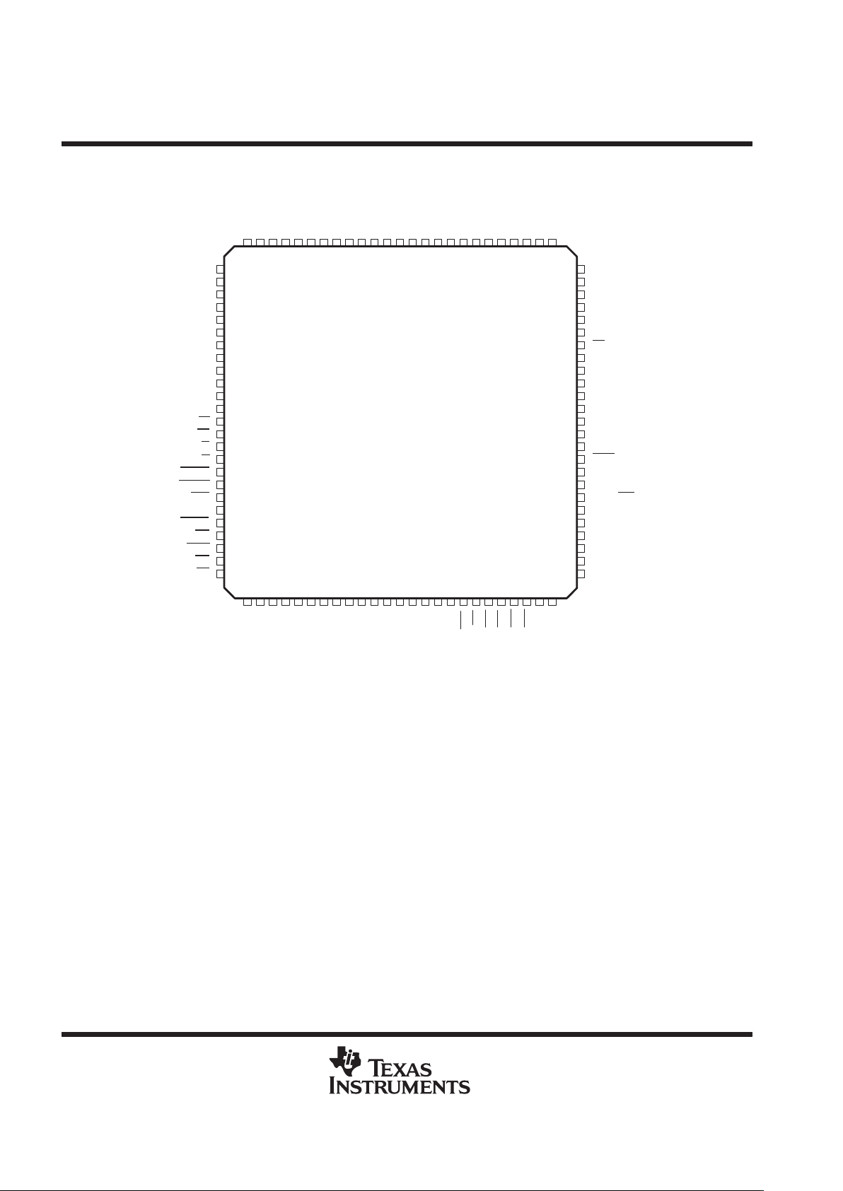
TMS320LC545
PBK PACKAGE
†
(TOP VIEW)
†
DV
DD
is the power supply for the I/O pins while CV
DD
is the power supply for the core CPU, and V
SS
is the ground for both the I/O pins and the
core CPU.
The ’54x signal descriptions table lists each terminal name, function, and operating mode(s) for the for the
TMS320LC545PBK (128-pin TQFP package).
For the ’LC545 (128-pin TQFP package), the letter B in front of CLKR, FSR, DR, CLKX, FSX, and DX pin names
denotes buffered serial port (BSP). No letter in front of CLKR, FSR, DR, CLKX, FSX, and DX pin names denotes
standard serial port.
TMS320C54x, TMS320LC54x, TMS320VC54x
FIXED-POINT DIGITAL SIGNAL PROCESSORS
SPRS039C – FEBRUARY 1996 – REVISED DECEMBER 1999
8
POST OFFICE BOX 1443 • HOUSTON, TEXAS 77251–1443
BCLKR
V
SS
A10
A11
A12
A13
A14
A15
CV
DD
V
SS
CV
DD
READY
PS
DS
IS
R/W
MSTRB
IOSTRB
MSC
XF
HOLDA
HOLD
BIO
MP/MC
1
2
3
4
5
6
7
8
9
10
11
12
13
14
15
16
17
18
19
20
21
22
23
24
25
76
77
78
79
80
81
82
83
84
85
86
87
88
89
90
91
92
93
94
95
96
97
98
99
100
75
74
73
72
71
70
69
68
67
66
65
64
63
62
61
60
59
58
57
56
55
54
53
52
51
50
49
48
47
46
45
44
43
42
41
40
39
38
37
36
35
34
33
32
31
30
29
28
27
26
A5
A4
A3
A2
A1
V
V
D14
D13
D12
D11
D10
D9
D8
D7
D6
DV
SS
CLKR
BFSR
FSR
BDR
DR
CLKX
DD
FSX
DD
SS
INT1
INT3
SS
V
SS
A6
D15
INT2
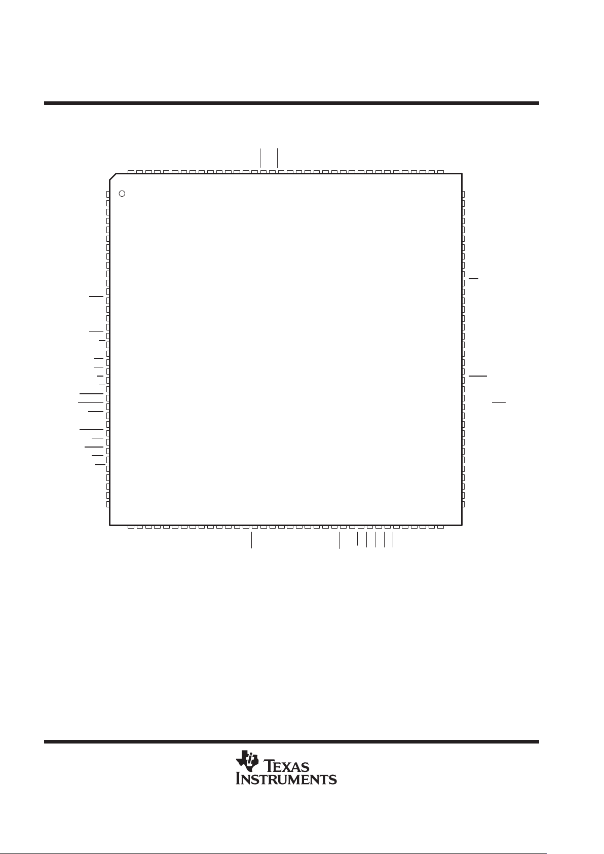
TMS320LC546
PZ PACKAGE
†
(TOP VIEW)
IAQ
A0
BCLKX
NMI
D5
D4
D3
D2
D1
D0
RS
X2/CLKIN
X1
V
SS
CV
DD
V
SS
TMS
TCK
TRST
TDI
TDO
EMU1/OFF
EMU0
TOUT
CLKMD3
CLKMD2
CLKMD1
CLKOUT
CNT
A9
A8
A7
SS
SS
DD
V
DV
V
V
CV
SS
V
BFSX
BDX
DX
IACK
DD
CV
INT0
CV
DD
V
DD
†
DV
DD
is the power supply for the I/O pins while CV
DD
is the power supply for the core CPU, and V
SS
is the ground for both the I/O pins and the
core CPU.
The ’54x signal descriptions table lists each terminal name, function, and operating mode(s) for the for the
TMS320LC546PZ (100-pin TQFP package).
For the ’LC546 (100-pin TQFP package), the letter B in front of CLKR, FSR, DR, FSX, and DX denotes buffered
serial port (BSP). No letter in front of CLKR, FSR, DR, FSX, and DX denotes standard serial port.

TMS320C54x, TMS320LC54x, TMS320VC54x
FIXED-POINT DIGITAL SIGNAL PROCESSORS
SPRS039C – FEBRUARY 1996 – REVISED DECEMBER 1999
9
POST OFFICE BOX 1443 • HOUSTON, TEXAS 77251–1443
CV
HDS1
A18
A17
V
SS
A16
D5
D4
D3
D2
D1
D0
RS
X2/CLKIN
X1
HD3
CLKOUT
V
SS
HPIENA
CV
DD
V
SS
TMS
TCK
TRST
TDI
TDO
EMU1/OFF
EMU0
TOUT
HD2
TEST1
CLKMD3
CLKMD2
CLKMD1
V
SS
DV
DD
BDX1
BFSX1
V
SS
A22
V
SS
DV
DD
A10
HD7
A11
A12
A13
A14
A15
CV
DD
HAS
V
SS
V
SS
CV
DD
HCS
HR/W
READY
PS
DS
IS
R/W
MSTRB
IOSTRB
MSC
XF
HOLDA
IAQ
HOLD
BIO
MP/MC
DV
DD
V
SS
BDR1
BFSR1
SS
V
144
A21
CV
143
142
141
A8
140
A7
139
A6
138
A5
137
A4
136
HD6
135
A3
134
A2
133
A1
132
A0
131
DV
130
129
128
127
V
126
125
HD5
124
D15
123
D14
122
D13
121
HD4
120
D12
119
D11
118
117
D9
116
D8
115
D7
114
D6
113
112
37
38
39
40
41
42
43
44
45
46
47
48
49
50
51
52
53
54
55
56
57
58
59
60
61
62
63
64
65
66
67
68
69
1
2
3
4
5
6
7
8
9
10
11
12
13
14
15
16
17
18
19
20
21
22
23
24
25
26
27
28
29
30
31
32
33
34
35
36
108
107
106
105
104
103
102
101
100
99
98
97
96
95
94
93
92
91
90
89
88
87
86
85
84
83
82
81
80
79
78
77
76
75
74
73
SS
V
BCLKR1
HCNTL0
SS
BCLKR0
TCLKR
BFSR0
TFSR/TADD
BDR0
HCNTL1
TDR
BCLKX0
TCLKX
SS
DD
SS
HD0
BDX0
TDX
IACK
HBIL
NMI
INT0
INT1
INT2
INT3
DD
HD1
SS
HRDY
HINT
111
V
110
A19
109
70
71
72
BCLKX1
SS
V
D10
TFSX/TFRM
SS
A20
DV
DD
CV
HDS2
SS
V
V
V
DV
V
CV
V
DD
DD
DD
DD
SS
TMS320LC548, TMS320LC549, and TMS320VC549
PGE PACKAGE
†‡
(TOP VIEW)
BFSX0
A9
†
NC = No connection
‡
DV
DD
is the power supply for the I/O pins while CV
DD
is the power supply for the core CPU, and V
SS
is the ground for both the I/O pins and the
core CPU.
The ’54x signal descriptions table lists each terminal name, function, and operating mode(s) for the
TMS320LC548PGE (144-pin TQFP package).
For the ’LC548, ’LC549 and ’VC549 (144-pin TQFP package), the letter B in front of CLKRn, FSRn, DRn,
CLKXn, FSXn, and DXn pin names denotes buffered serial port (BSP), where n = 0 or 1 port. The letter T in
front of CLKR, FSR, DR, CLKX, FSX, and DX pin names denotes time-division multiplexed (TDM) serial port.
TMS320C54x, TMS320LC54x, TMS320VC54x
FIXED-POINT DIGITAL SIGNAL PROCESSORS
SPRS039C – FEBRUARY 1996 – REVISED DECEMBER 1999
10
POST OFFICE BOX 1443 • HOUSTON, TEXAS 77251–1443
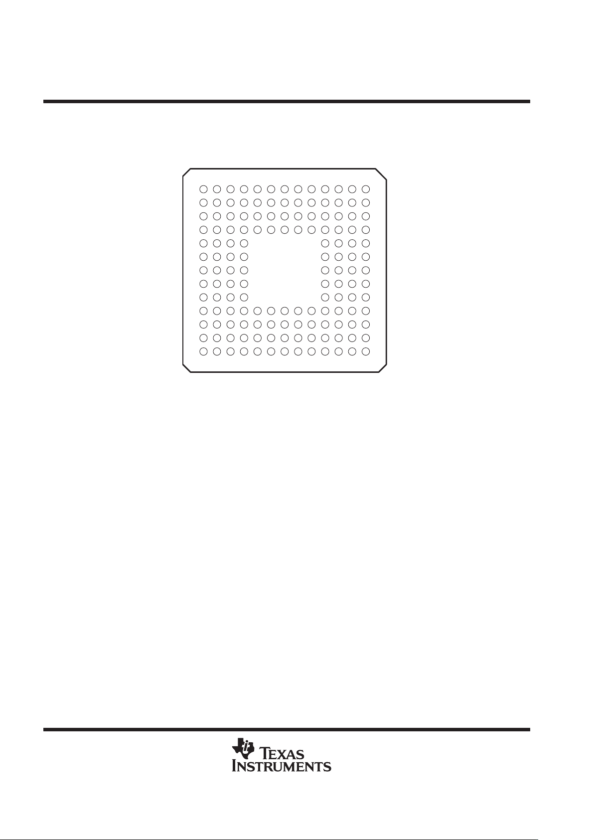
TMS320LC548, TMS320LC549, TMS320VC549
GGU PACKAGE
(BOTTOM VIEW)
A
B
D
C
E
F
H
J
L
M
K
N
G
12
3456781012 1113 9
The pin assignments table to follow lists each signal quadrant and BGA ball pin number for the TMS320LC548,
TMS320LC549, and TMS320VC549 (144-pin BGA package).
The ’54x signal descriptions table lists each terminal name, function, and operating mode(s) for the
TMS320LC548GGU, TMS320LC549GGU, and TMS320VC549GGU.
TMS320C54x, TMS320LC54x, TMS320VC54x
FIXED-POINT DIGITAL SIGNAL PROCESSORS
SPRS039C – FEBRUARY 1996 – REVISED DECEMBER 1999
11
POST OFFICE BOX 1443 • HOUSTON, TEXAS 77251–1443
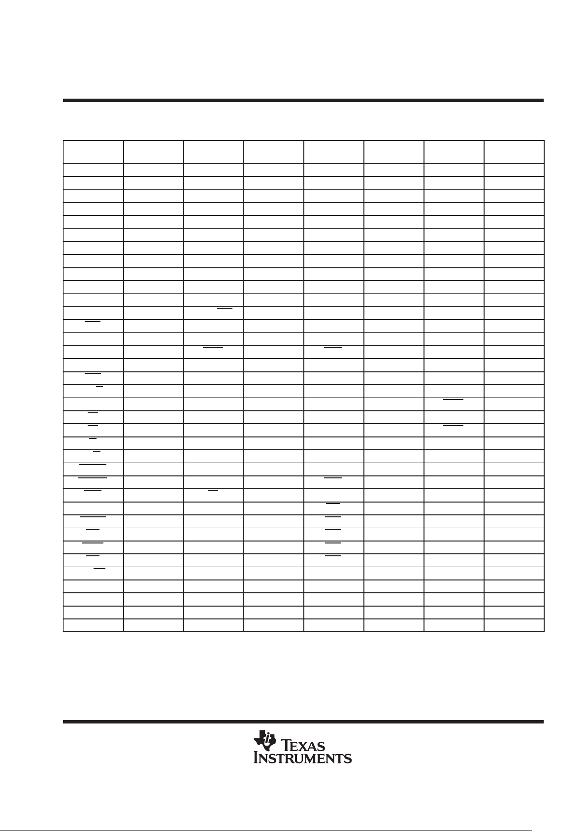
Pin Assignments for the TMS320LC548GGU, TMS320LC549GGU, and TMS320VC549GGU
(144-Pin BGA Package)
†
SIGNAL
QUADRANT 1
BGA BALL #
SIGNAL
QUADRANT 2
BGA BALL #
SIGNAL
QUADRANT 3
BGA BALL #
SIGNAL
QUADRANT 4
BGA BALL #
V
SS
A1 BFSX1 N13 V
SS
N1 A19 A13
A22 B1 BDX1 M13 BCLKR1 N2 A20 A12
V
SS
C2 DV
DD
L12 HCNTL0 M3 V
SS
B11
DV
DD
C1 V
SS
L13 V
SS
N3 DV
DD
A11
A10 D4 CLKMD1 K10 BCLKR0 K4 D6 D10
HD7 D3 CLKMD2 K11 TCLKR L4 D7 C10
A11 D2 CLKMD3 K12 BFSR0 M4 D8 B10
A12 D1 TEST1 K13 TFSR/TADD N4 D9 A10
A13 E4 HD2 J10 BDR0 K5 D10 D9
A14 E3 TOUT J11 HCNTL1 L5 D11 C9
A15 E2 EMU0 J12 TDR M5 D12 B9
CV
DD
E1 EMU1/OFF J13 BCLKX0 N5 HD4 A9
HAS F4 TDO H10 TCLKX K6 D13 D8
V
SS
F3 TDI H11 V
SS
L6 D14 C8
V
SS
F2 TRST H12 HINT M6 D15 B8
CV
DD
F1 TCK H13 CVDD N6 HD5 A8
HCS G2 TMS G12 BFSX0 M7 CV
DD
B7
HR/W G1 V
SS
G13 TFSX/TFRM N7 V
SS
A7
READY G3 CV
DD
G11 HRDY L7 HDS1 C7
PS G4 HPIENA G10 DV
DD
K7 V
SS
D7
DS H1 V
SS
F13 V
SS
N8 HDS2 A6
IS H2 CLKOUT F12 HD0 M8 DV
DD
B6
R/W H3 HD3 F11 BDX0 L8 A0 C6
MSTRB H4 X1 F10 TDX K8 A1 D6
IOSTRB J1 X2/CLKIN E13 IACK N9 A2 A5
MSC J2 RS E12 HBIL M9 A3 B5
XF J3 D0 E11 NMI L9 HD6 C5
HOLDA J4 D1 E10 INT0 K9 A4 D5
IAQ K1 D2 D13 INT1 N10 A5 A4
HOLD K2 D3 D12 INT2 M10 A6 B4
BIO K3 D4 D11 INT3 L10 A7 C4
MP/MC L1 D5 C13 CV
DD
N11 A8 A3
DV
DD
L2 A16 C12 HD1 M11 A9 B3
V
SS
L3 V
SS
C11 V
SS
L11 CV
DD
C3
BDR1 M1 A17 B13 BCLKX1 N12 A21 A2
BFSR1 M2 A18 B12 V
SS
M12 V
SS
B2
†
DV
DD
is the power supply for the I/O pins while CV
DD
is the power supply for the core CPU, and V
SS
is the ground for both the I/O pins and the
core CPU.
TMS320C54x, TMS320LC54x, TMS320VC54x
FIXED-POINT DIGITAL SIGNAL PROCESSORS
SPRS039C – FEBRUARY 1996 – REVISED DECEMBER 1999
12
POST OFFICE BOX 1443 • HOUSTON, TEXAS 77251–1443
’54x Signal Descriptions
TERMINAL
NAME TYPE
†
DESCRIPTION
DATA SIGNALS
A22 (MSB)
A21
A20
A19
A18
A17
A16
A15
A14
A13
A12
A11
A10
A9
A8
A7
A6
A5
A4
A3
A2
A1
A0 (LSB)
O/Z
Parallel port address bus A22 (MSB) through A0 (LSB). The sixteen LSBs (A15–A0) are multiplexed to address
external data/program memory or I/O. A15–A0 are placed in the high-impedance state in the hold mode. A15–A0
also go into the high-impedance state when EMU1/OFF
is low. The seven MSBs (A22 to A16) are used for
extended program memory addressing (’548 and ’549 only).
On the ’548 and ’549 devices, the address bus have a feature called bus holder that eliminates passive
components and the power dissipation associated with it. The bus holders keep the address bus at the previous
logic level when the bus goes into a high-impedance state. The bus holders on the address bus are always
enabled.
D15 (MSB)
D14
D13
D12
D11
D10
D9
D8
D7
D6
D5
D4
D3
D2
D1
D0 (LSB)
I/O/Z
Parallel port data bus D15 (MSB) through D0 (LSB). D15–D0 are multiplexed to transfer data between the core
CPU and external data/program memory or I/O devices. D15–D0 are placed in the high-impedance state when
not output or when RS
or HOLD is asserted. D15–D0 also go into the high-impedance state when EMU1/OFF
is low.
The data bus has a feature called bus holder that eliminates passive components and the power dissipation
associated with it. The bus holders keep the data bus at the previous logic level when the bus goes into a
high-impedance state. These bus holders are enabled or disabled by the BH bit in the bank switching control
register (BSCR).
INITIALIZATION, INTERRUPT AND RESET OPERATIONS
IACK O/Z
Interrupt acknowledge signal. IACK indicates the receipt of an interrupt and that the program counter is fetching
the interrupt vector location designated by A15–0. IACK
also goes into the high-impedance state when
EMU1/OFF
is low.
INT0
INT1
INT2
INT3
I
External user interrupt inputs. INT0–INT3 are prioritized and are maskable by the interrupt mask register and the
interrupt mode bit. INT0
–INT3 can be polled and reset by the interrupt flag register.
†
I = Input, O = Output, Z = High impedance

TMS320C54x, TMS320LC54x, TMS320VC54x
FIXED-POINT DIGITAL SIGNAL PROCESSORS
SPRS039C – FEBRUARY 1996 – REVISED DECEMBER 1999
13
POST OFFICE BOX 1443 • HOUSTON, TEXAS 77251–1443
’54x Signal Descriptions (Continued)
TERMINAL
DESCRIPTION
NAME
DESCRIPTION
TYPE
†
INITIALIZATION, INTERRUPT AND RESET OPERATIONS (CONTINUED)
NMI I
Nonmaskable interrupt. NMI is an external interrupt that cannot be masked by way of the INTM or the IMR. When
NMI
is activated, the processor traps to the appropriate vector location.
RS I
Reset input. RS causes the DSP to terminate execution and forces the program counter to 0FF80h. When RS
is brought to a high level, execution begins at location 0FF80h of the program memory. RS affects various
registers and status bits.
MP/MC I
Microprocessor/microcomputer mode-select pin. If active-low at reset (microcomputer mode), MP/MC causes
the internal program ROM to be mapped into the upper program memory space. In the microprocessor mode,
off-chip memory and its corresponding addresses (instead of internal program ROM) are accessed by the DSP.
CNT I
I/O level select. For 5-V operation, all input and output voltage levels are TTL-compatible when CNT is pulled
down to a low level. For 3-V operation with CMOS-compatible I/O interface levels, CNT is pulled to a high level.
MULTIPROCESSING SIGNALS
BIO I
Branch control input. A branch can be conditionally executed when BIO is active. If low, the processor executes
the conditional instruction. The BIO
condition is sampled during the decode phase of the pipeline for the XC
instruction, and all other instructions sample BIO
during the read phase of the pipeline.
XF O/Z
External flag output (latched software-programmable signal). XF is set high by the SSBX XF instruction, set low
by RSBX XF instruction or by loading the ST1 status register. XF is used for signaling other processors in
multiprocessor configurations or as a general-purpose output pin. XF goes into the high-impedance state when
OFF
is low, and is set high at reset.
MEMORY CONTROL SIGNALS
DS
PS
IS
O/Z
Data, program, and I/O space select signals. DS, PS, and IS are always high unless driven low for communicating
to a particular external space. Active period corresponds to valid address information. Placed into a
high-impedance state in hold mode. DS
, PS, and IS also go into the high-impedance state when EMU1/OFF is
low.
MSTRB O/Z
Memory strobe signal. MSTRB is always high unless low-level asserted to indicate an external bus access to data
or program memory. Placed in high-impedance state in hold mode. MSTRB
also goes into the high-impedance
state when OFF
is low.
READY I
Data-ready input. READY indicates that an external device is prepared for a bus transaction to be completed.
If the device is not ready (READY is low), the processor waits one cycle and checks READY again. Note that the
processor performs ready-detection if at least two software wait states are programmed. The READY signal is
not sampled until the completion of the software wait states.
R/W O/Z
Read/write signal. R/W indicates transfer direction during communication to an external device and is normally
high (in read mode), unless asserted low when the DSP performs a write operation. Placed in the high-impedance
state in hold mode, R/W
also goes into the high-impedance state when EMU1/OFF is low.
IOSTRB O/Z
I/O strobe signal. IOSTRB is always high unless low level asserted to indicate an external bus access to an I/O
device. Placed in high-impedance state in hold mode. IOSTRB
also goes into the high-impedance state when
EMU1/OFF
is low.
HOLD I
Hold input. HOLD is asserted to request control of the address, data, and control lines. When acknowledged by
the ’54x, these lines go into high-impedance state.
HOLDA O/Z
Hold acknowledge signal. HOLDA indicates to the external circuitry that the processor is in a hold state and that
the address, data, and control lines are in a high-impedance state, allowing them to be available to the external
circuitry. HOLDA
also goes into the high-impedance state when EMU1/OFF is low.
MSC O/Z
Microstate complete signal. Goes low on CLKOUT falling at the start of the first software wait state. Remains low
until one CLKOUT cycle before the last programmed software wait state. If connected to the READY line, MSC
forces one external wait state after the last internal wait state has been completed. MSC also goes into the
high-impedance state when EM1/OFF
is low.
†
I = Input, O = Output, Z = High impedance
TMS320C54x, TMS320LC54x, TMS320VC54x
FIXED-POINT DIGITAL SIGNAL PROCESSORS
SPRS039C – FEBRUARY 1996 – REVISED DECEMBER 1999
14
POST OFFICE BOX 1443 • HOUSTON, TEXAS 77251–1443
’54x Signal Descriptions (Continued)
TERMINAL
DESCRIPTION
NAME
DESCRIPTION
TYPE
†
MEMORY CONTROL SIGNALS (CONTINUED)
IAQ O/Z
Instruction acquisition signal. IAQ is asserted (active low) when there is an instruction address on the address
bus and goes into the high-impedance state when EMU1/OFF
is low.
OSCILLATOR/TIMER SIGNALS
CLKOUT O/Z
Master clock output signal. CLKOUT cycles at the machine-cycle rate of the CPU. The internal machine cycle
is bounded by the falling edges of this signal. CLKOUT also goes into the high-impedance state when EMU1/OFF
is low.
CLKMD1
CLKMD2
CLKMD3
I
Clock mode external/internal input signals. CLKMD1, CLKMD2, and CLKMD3 allow you to select and configure
different clock modes, such as crystal, external clock, and various PLL factors. Refer to PLL section for a detailed
functional description of these pins.
X2/CLKIN I
Input pin to internal oscillator from the crystal. If the internal (crystal) oscillator is not being used, a clock can
become input to the device using this pin. The internal machine cycle time is determined by the clock
operating-mode pins (CLKMD1, CLKMD2 and CLKMD3).
X1 O
Output pin from the internal oscillator for the crystal. If the internal oscillator is not used, X1 should be left
unconnected. X1 does not go into the high-impedance state when EMU1/OFF
is low.
TOUT O/Z
Timer output. TOUT signals a pulse when the on-chip timer counts down past zero. The pulse is a CLKOUT -cycle
wide. TOUT also goes into the high-impedance state when EMU1/OFF
is low.
BUFFERED SERIAL PORT 0 AND BUFFERED SERIAL PORT 1 SIGNALS
BCLKR0
BCLKR1
I
Receive clocks. External clock signal for clocking data from the data-receive (DR) pin into the buffered serial port
receive shift registers (RSRs). Must be present during buffered serial port transfers. If the buffered serial port is
not being used, BCLKR0 and BCLKR1 can be sampled as an input by way of IN0 bit of the SPC register.
BCLKX0
BCLKX1
I/O/Z
Transmit clock. Clock signal for clocking data from the serial port transmit shift register (XSR) to the data transmit
(DX) pin. BCLKX can be an input if MCM in the serial port control register is cleared to 0. It also can be driven
by the device at 1/(CLKDV + 1) where CLKDV range is 0–31 CLKOUT frequency when MCM is set to 1. If the
buffered serial port is not used, BCLKX can be sampled as an input by way of IN1 of the SPC register . BCLKX0
and BCLKX1 go into the high-impedance state when OFF
is low.
BDR0
BDR1
I Buffered serial-data-receive input. Serial data is received in the RSR by BDR0/BDR1.
BDX0
BDX1
O/Z
Buffered serial-port-transmit output. Serial data is transmitted from the XSR by way of BDX. BDX0 and BDX1 are
placed in the high-impedance state when not transmitting and when EMU1/OFF
is low.
BFSR0
BFSR1
I
Frame synchronization pulse for receive input. The falling edge of the BFSR pulse initiates the data-receive
process, beginning the clocking of the RSR.
BFSX0
BFSX1
I/O/Z
Frame synchronization pulse for transmit input/output. The falling edge of the BFSX pulse initiates the
data-transmit process, beginning the clocking of the XSR. Following reset, the default operating condition of
BFSX is an input. BFSX0 and BFSX1 can be selected by software to be an output when TXM in the serial control
register is set to 1. This pin goes into the high-impedance state when EMU1/OFF
is low.
SERIAL PORT 0 AND SERIAL PORT 1 SIGNALS
CLKR0
CLKR1
I
Receive clocks. External clock signal for clocking data from the data receive (DR) pin into the serial port receive
shift register (RSR). Must be present during serial port transfers. If the serial port is not being used, CLKR0 and
CLKR1 can be sampled as an input via IN0 bit of the SPC register.
CLKX0
CLKX1
I/O/Z
Transmit clock. Clock signal for clocking data from the serial port transmit shift register (XSR) to the data transmit
(DX) pin. CLKX can be an input if MCM in the serial port control register is cleared to 0. It also can be driven by
the device at 1/4 CLKOUT frequency when MCM is set to 1. If the serial port is not used, CLKX can be sampled
as an input via IN1 of the SPC register. CLKX0 and CLKX1 go into the high-impedance state when EMU1/OFF
is low.
DR0
DR1
I
Serial-data-receive input. Serial data is received in the RSR by DR.
†
I = Input, O = Output, Z = High impedance
TMS320C54x, TMS320LC54x, TMS320VC54x
FIXED-POINT DIGITAL SIGNAL PROCESSORS
SPRS039C – FEBRUARY 1996 – REVISED DECEMBER 1999
15
POST OFFICE BOX 1443 • HOUSTON, TEXAS 77251–1443
’54x Signal Descriptions (Continued)
TERMINAL
DESCRIPTION
NAME
DESCRIPTION
TYPE
†
SERIAL PORT 0 AND SERIAL PORT 1 SIGNALS (CONTINUED)
DX0
DX1
O/Z
Serial port transmit output. Serial data is transmitted from the XSR via DX. DX0 and DX1 are placed in the
high-impedance state when not transmitting and when EMU1/OFF
is low.
FSR0
FSR1
I
Frame synchronization pulse for receive input. The falling edge of the FSR pulse initiates the data-receive
process, beginning the clocking of the RSR.
FSX0
FSX1
I/O/Z
Frame synchronization pulse for transmit input/output. The falling edge of the FSX pulse initiates the data transmit
process, beginning the clocking of the XSR. Following reset, the default operating condition of FSX is an input.
FSX0 and FSX1 can be selected by software to be an output when TXM in the serial control register is set to 1.
This pin goes into the high-impedance state when EMU1/OFF is low.
TDM SERIAL PORT SIGNALS
TCLKR I TDM receive clock input
TDR I TDM serial data-receive input
TFSR/TADD I/O TDM receive frame synchronization or TDM address
TCLKX I/O/Z TDM transmit clock
TDX O/Z TDM serial data-transmit output
TFSX/TFRM I/O/Z TDM transmit frame synchronization
HOST-PORT INTERFACE SIGNALS
HD0–HD7 I/O/Z
Parallel bidirectional data bus. HD0–HD7 are placed in the high-impedance state when not outputting data. The
signals go into the high-impedance state when EMU1/OFF
is low. These pins each have bus holders similar to
those on the address/data bus, but which are always enabled.
HCNTL0
HCNTL1
I Control inputs
HBIL I Byte-identification input
HCS I Chip-select input
HDS1
HDS2
I Data strobe inputs
HAS I Address strobe input
HR/W I Read/write input
HRDY O/Z Ready output. This signal goes into the high-impedance state when EMU1/OFF is low.
HINT O/Z
Interrupt output. When the DSP is in reset, this signal is driven high. The signal goes into the high-impedance
state when EMU1/OFF
is low.
HPIENA I
HPI module select input. This signal must be tied to a logic 1 state to have HPI selected. If this input is left open
or connected to ground, the HPI module will not be selected, internal pullup for the HPI input pins are enabled,
and the HPI data bus has keepers set. This input is provided with an internal pull-down resistor which is active
only when RS
is low. HPIENA is sampled when RS goes high and ignored until RS goes low again. Refer to the
Electrical Characteristics section for the input current requirements for this pin.
SUPPLY PINS
CV
DD
Supply +V
DD
. CV
DD
is the dedicated power supply for the core CPU.
DV
DD
Supply +V
DD
. DV
DD
is the dedicated power supply for I/O pins.
V
SS
Supply Ground. V
SS
is the dedicated power ground for the device.
†
I = Input, O = Output, Z = High impedance
TMS320C54x, TMS320LC54x, TMS320VC54x
FIXED-POINT DIGITAL SIGNAL PROCESSORS
SPRS039C – FEBRUARY 1996 – REVISED DECEMBER 1999
16
POST OFFICE BOX 1443 • HOUSTON, TEXAS 77251–1443
’54x Signal Descriptions (Continued)
TERMINAL
DESCRIPTION
NAME
DESCRIPTION
TYPE
†
IEEE1149.1 TEST PINS
TCK I
IEEE standard 1149.1 test clock. Pin with internal pullup device. This is normally a free-running clock signal with
a 50% duty cycle. The changes on the test-access port (TAP) of input signals TMS and TDI are clocked into the
TAP controller, instruction register , or selected test data register on the rising edge of TCK. Changes at the T AP
output signal (TDO) occur on the falling edge of TCK.
TDI I
IEEE standard 1149.1 test data input. Pin with internal pullup device. TDI is clocked into the selected register
(instruction or data) on a rising edge of TCK.
TDO O/Z
IEEE standard 1149.1 test data output. The contents of the selected register (instruction or data) is shifted out
of TDO on the falling edge of TCK. TDO is in the high-impedance state except when the scanning of data is in
progress. TDO also goes into the high-impedance state when EMU1/OFF
is low.
TMS I
IEEE standard 1149.1 test mode select. Pin with internal pullup device. This serial control input is clocked into
the TAP controller on the rising edge of TCK.
TRST I
IEEE standard 1149.1 test reset. TRST, when high, gives the IEEE standard 1149.1 scan system control of the
operations of the device. If TRST
is not connected or driven low, the device operates in its functional mode, and
the IEEE standard 1149.1 signals are ignored. Pin with internal pulldown device.
EMU0 I/O/Z
Emulator interrupt 0 pin. When TRST is driven low, EMU0 must be high for the activation of the EMU1/OFF
condition. When TRST is driven high, EMU0 is used as an interrupt to or from the emulator system and is defined
as input/output by way of IEEE standard 1149.1 scan system.
EMU1/OFF I/O/Z
Emulator interrupt 1 pin/disable all outputs. When TRST is driven high, EMU1/OFF is used as an interrupt to or
from the emulator system and is defined as input/output by way of IEEE standard 1149.1 scan system. When
TRST
is driven low, EMU1/OFF is configured as OFF. The EMU1/OFF signal, when active low, puts all output
drivers into the high-impedance state. Note that OFF
is used exclusively for testing and emulation purposes (not
for multiprocessing applications). Therefore, for the OFF
condition, the following conditions apply:
TRST
= low,
EMU0 = high
EMU1/OFF
= low
DEVICE TEST PIN
TEST1 I
Test1 – Reserved for internal use only (’LC548, ’LC549, and ’VC549 only). This pin must not be connected
(NC).
†
I = Input, O = Output, Z = High impedance
architecture
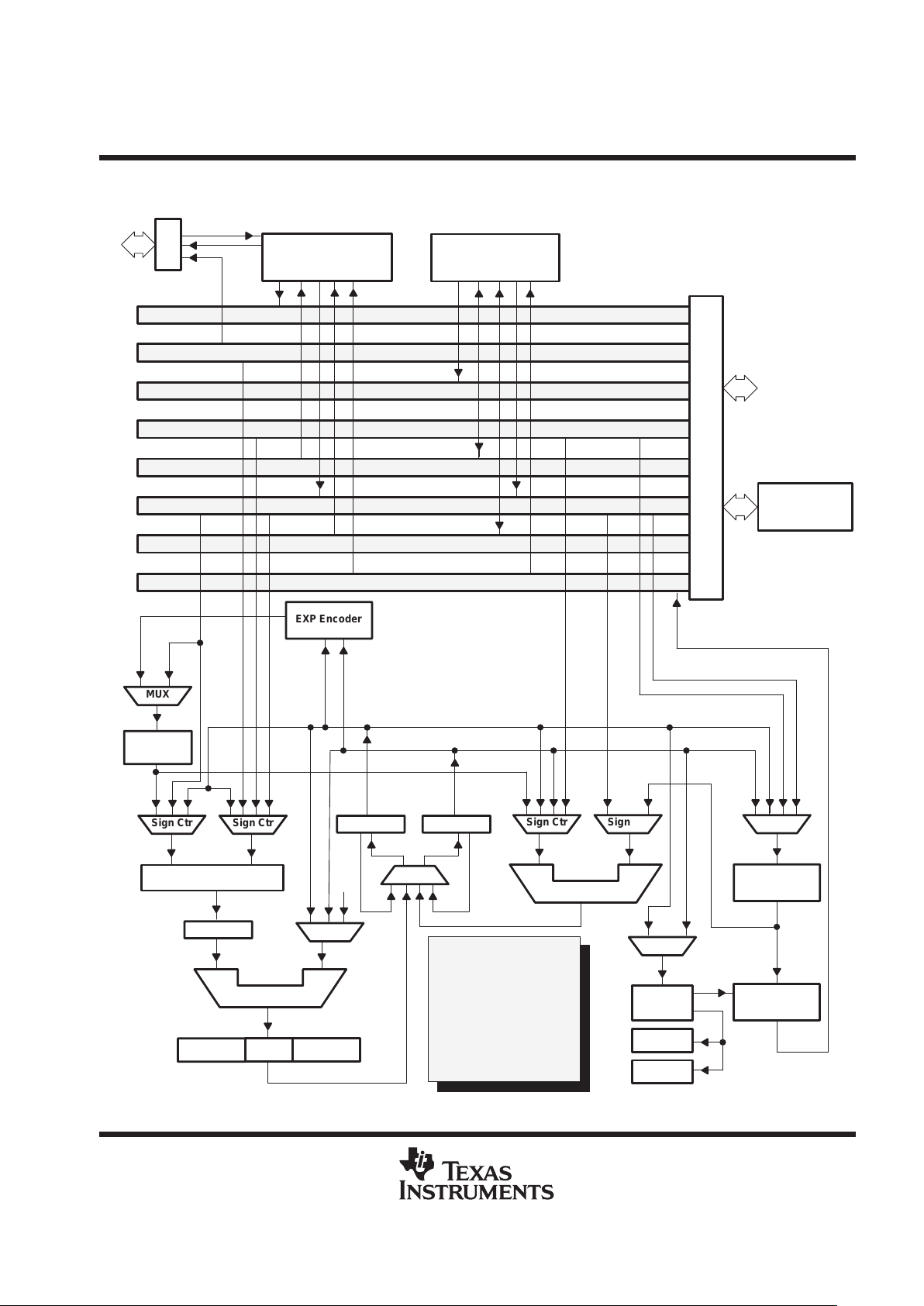
The ’54x DSPs use an advanced, modified Harvard architecture that maximizes processing power by
maintaining three separate bus structures for data memory and one for program memory. Separate program
and data spaces allow simultaneous access to program instructions and data, providing a high degree of
parallelism. For example, two read and one write operations can be performed in a single cycle. Instructions
with parallel store and application-specific instructions fully utilize this architecture. In addition, data can be
transferred between data and program spaces. Such parallelism supports a powerful set of arithmetic, logic,
and bit-manipulation operations that can all be performed in a single machine cycle. In addition, the ’54x include
the control mechanisms to manage interrupts, repeated operations, and function calls.
The functional block diagram includes the principal blocks and bus structure in the ’54x devices.
TMS320C54x, TMS320LC54x, TMS320VC54x
FIXED-POINT DIGITAL SIGNAL PROCESSORS
SPRS039C – FEBRUARY 1996 – REVISED DECEMBER 1999
17
POST OFFICE BOX 1443 • HOUSTON, TEXAS 77251–1443
functional block diagram of the ’54x internal hardware
M
P
A
T Register
A(40) B(40)
Multiplier (17 × 17)
Fractional
MUX
0
Adder(40)
ZERO ROUND
SAT
System Control
Interface
Program Address Generation
Logic (PAGEN)
Data Address Generation
Logic (DAGEN)
PC, IPTR, RC,
BRC, RSA, REA
ARAU0, ARAU1,
AR0–AR7
ARP, BK, DP, SP
Memory
And
External
Interface
Peripherals
(Serial Ports,
HPI, etc.)
PAB
PB
CAB
CB
DAB
DB
EAB
EB
Sign Ctr Sign Ctr
MUX
EXP Encoder
Sign Ctr Sign Ctr Sign Ctr
MUX
ALU(40)
Barrel Shifter
MUX
COMP
TRN
TC
MSW/LSW
Select
CABD
S
BA
SDABCTCDADT
BU
A
A
B
XD
AB
A Accumulator A
B Accumulator B
C CB Data Bus
D DB Data Bus
E EB Data Bus
M MAC Unit
P PB Program Bus
S Barrel Shifter
T T Register
U ALU
Legend:
E

TMS320C54x, TMS320LC54x, TMS320VC54x
FIXED-POINT DIGITAL SIGNAL PROCESSORS
SPRS039C – FEBRUARY 1996 – REVISED DECEMBER 1999
18
POST OFFICE BOX 1443 • HOUSTON, TEXAS 77251–1443
central processing unit (CPU)
The CPU of the ’54x devices contains:
D A 40-bit arithmetic logic unit (ALU)
D Two 40-bit accumulators
D A barrel shifter
D A 17 × 17-bit multiplier/adder
D A compare, select and store unit (CSSU)
arithmetic logic unit (ALU)
The ’54x devices perform 2s-complement arithmetic using: a 40-bit arithmetic logic unit (ALU) and two 40-bit
accumulators (ACCA and ACCB). The ALU also can perform Boolean operations.
The ALU can function as two 16-bit ALUs and perform two 16-bit operations simultaneously when the C16 bit
in status register 1 (ST1) is set.
accumulators
The accumulators, ACCA and ACCB, store the output from the ALU or the multiplier / adder block; the
accumulators can also provide a second input to the ALU or the multiplier/ adder. The accumulators are divided
into three parts:
D Guard bits (bits 32–39)
D A high-order word (bits 16–31)
D A low-order word (bits 0–15)
Instructions are provided for storing the guard bits, the high- and the low-order accumulator words in data
memory , and for manipulating 32-bit accumulator words in or out of data memory. Also, any of the accumulators
can be used as temporary storage for the other.
barrel shifter
The ’54x’s barrel shifter has a 40-bit input connected to the accumulator, or data memory
(CB, DB) and a 40-bit output connected to the ALU, or data memory (EB). The barrel shifter produces a left shift
of 0 to 31 bits and a right shift of 0 to 16 bits on the input data. The shift requirements are defined in the shift-count
field
(ASM) of ST1 or defined in the temporary register (TREG), which is designated as a shift-count register.
This shifter and the exponent detector normalize the values in an accumulator in a single cycle. The least
significant bits (LSBs) of the output are filled with 0s and the most significant bits (MSBs) can be either zero-filled
or sign-extended, depending on the state of the sign-extended mode bit (SXM) of ST1. Additional shift
capabilities enable the processor to perform numerical scaling, bit extraction, extended arithmetic, and overflow
prevention operations.
multiplier/adder
The multiplier/ adder performs 17 × 17-bit 2s-complement multiplication with a 40-bit accumulation in a single
instruction cycle. The multiplier/ adder block consists of several elements: a multiplier, adder , signed/ unsigned
input control, fractional control, a zero detector, a rounder (2s-complement), overflow / saturation logic, and
TREG. The multiplier has two inputs: one input is selected from the TREG, a data-memory operand, or an
accumulator; the other is selected from the program memory, the data memory, an accumulator, or an
immediate value. The fast on-chip multiplier allows the ’54x to perform operations such as convolution,
correlation, and filtering efficiently.
In addition, the multiplier and ALU together execute multiply/accumulate (MAC) computations and ALU
operations in parallel in a single instruction cycle. This function is used in determining the Euclid distance, and
in implementing symmetrical and least mean square (LMS) filters, which are required for complex DSP
algorithms.

TMS320C54x, TMS320LC54x, TMS320VC54x
FIXED-POINT DIGITAL SIGNAL PROCESSORS
SPRS039C – FEBRUARY 1996 – REVISED DECEMBER 1999
19
POST OFFICE BOX 1443 • HOUSTON, TEXAS 77251–1443
compare, select and store unit (CSSU)
The compare, select and store unit (CSSU) performs maximum comparisons between the accumulator’s high
and low word, allows the test/control (TC) flag bit of status register 0 (ST0) and the transition (TRN) register
to keep their transition histories, and selects the larger word in the accumulator to be stored in data memory.
The CSSU also accelerates Viterbi-type butterfly computation with optimized on-chip hardware.
program control
Program control is provided by several hardware and software mechanisms:
D The program controller decodes instructions, manages the pipeline, stores the status of operations, and
decodes conditional operations. Some of the hardware elements included in the program controller are the
program counter, the status and control register, the stack, and the address-generation logic.
D Some of the software mechanisms used for program control include branches, calls, conditional
instructions, a repeat instruction, reset, and interrupts.
power-down modes
There are three power-down modes, activated by the IDLE1, IDLE2, and IDLE3 instructions. In these modes,
the ’54x devices enter a dormant state and dissipate considerably less power than in normal operation. The
IDLE1 instruction is used to shut down the CPU. The IDLE2 instruction is used to shut down the CPU and on-chip
peripherals. The IDLE3 instruction is used to shut down the ’54x processor completely . This instruction stops
the PLL circuitry as well as the CPU and peripherals.
bus structure
The ’54x device architecture is built around eight major 16-bit buses:
D One program-read bus (PB), which carries the instruction code and immediate operands from program
memory
D Two data-read buses (CB, DB) and one data-write bus (EB), which interconnect to various elements, such
as the CPU, data-address generation logic, program-address generation logic, on-chip peripherals, and
data memory
– The CB and DB carry the operands read from data memory.
– The EB carries the data to be written to memory.
D Four address buses (PAB, CAB, DAB, and EAB), which carry the addresses needed for instruction
execution
The ’54x devices have the capability to generate up to two data-memory addresses per cycle, which are stored
into two auxiliary register arithmetic units (ARAU0 and ARAU1).
The PB can carry data operands stored in program space (for instance, a coefficient table) to the multiplier for
multiply/accumulate operations or to a destination in data space for the data move instruction. This capability
allows implementation of single-cycle three-operand instructions such as FIRS.
The ’54x devices also have an on-chip bidirectional bus for accessing on-chip peripherals; this bus is connected
to DB and EB through the bus exchanger in the CPU interface. Accesses using this bus can require more than
two cycles for reads and writes depending on the peripheral’s structure.
The ’54x devices can have bus keepers connected to the data bus. Bus keepers ensure that the data bus does
not float. When bus keepers are enabled, the data bus maintains its previous level. Setting bit 1 of the bank
switching control register (BSCR) enables bus keepers and clearing bit 1 disables the bus keepers. A reset
automatically disables the bus keepers.
TMS320C54x, TMS320LC54x, TMS320VC54x
FIXED-POINT DIGITAL SIGNAL PROCESSORS
SPRS039C – FEBRUARY 1996 – REVISED DECEMBER 1999
20
POST OFFICE BOX 1443 • HOUSTON, TEXAS 77251–1443
bus structure (continued)
The ’548 and ’549 devices also have equivalent bus keepers connected to the address bus. The bus keepers
ensure the address bus does not float when in high-impedance. For the ’548 and ’549 devices, the bus keepers
are always enabled.
Table 2 summarizes the buses used by various types of accesses.
Table 2. Bus Usage for Accesses
ACCESS TYPE
ADDRESS BUS
PROGRAM
BUS
DATA BUS
ACCESS
TYPE
PAB CAB DAB EAB PB CB DB EB
Program read √ √
Program write √ √
Data single read √ √
Data dual read √ √ √ √
Data long (32-bit) read √(hw) √(lw) √(hw) √(lw)
Data single write √ √
Data read/data write √ √ √ √
Dual read/coefficient read √ √ √ √ √ √
Peripheral read √ √
Peripheral write √ √
Legend:
hw = high 16-bit word
lw = low 16-bit word
memory
The total memory address range for the host of ’54x devices is 192K 16-bit words. The ’548 and ’549 devices
have 8M-word program memory . The memory space is divided into three specific memory segments: 64K-word
program, 64K-word data, and 64K-word I /O. The program memory space contains the instructions to be
executed as well as tables used in execution. The data memory space stores data used by the instructions. The
I/O memory space interfaces to external memory-mapped peripherals and can also serve as extra data storage
space.
The parallel nature of the architecture of these DSPs allows them to perform four concurrent memory operations
in any given machine cycle: fetching an instruction, reading two operands, and writing an operand. The four
parallel buses are the program-read bus (PB), the data-write bus (EB) and the two data-read buses (CB and
DB). Each bus accesses different memory spaces for different aspects of the DSP’s operation. Additionally , this
architecture allows dual-operand reads, 32-bit-long word accesses, and a single read with a parallel store.
The ’54x DSPs include on-chip memory to aid in system performance and integration.
on-chip ROM
The ’C541 and ’LC541 feature a 28K-word
×16-bit on-chip maskable ROM. 8K words of the ’C541 and ’LC541
ROM can be mapped into program and data memory space if the data ROM (DROM) bit in the processor mode
status (PMST) register is set. This allows an instruction to use data stored in the ROM as an operand.
The ’LC545/’LC546 all feature a 48K-word × 16-bit on-chip maskable ROM. 16K words of the ROM on these
devices can be mapped into program and data memory space if the DROM bit in the PMST register is set.
The ’C542/’LC542/’LC543/ ’LC548 all feature 2K-word × 16-bit on-chip ROM.
The ’LC549 and ’VC549 feature 16K-word x 16-bit on-chip ROM.

TMS320C54x, TMS320LC54x, TMS320VC54x
FIXED-POINT DIGITAL SIGNAL PROCESSORS
SPRS039C – FEBRUARY 1996 – REVISED DECEMBER 1999
21
POST OFFICE BOX 1443 • HOUSTON, TEXAS 77251–1443
on-chip ROM (continued)
Customers can arrange to have the ROM of the ’54x programmed with contents unique to any particular
application.
on-chip dual-access RAM (DARAM)
The ’541 devices have a 5K-word
× 16-bit on-chip DARAM (5 blocks of 1K-word each).
The ’542 and ’543 devices have a 10K-word × 16-bit on-chip DARAM (5 blocks of 2K-word each).
The ’545 and ’546 devices have a 6K-word
× 16-bit on-chip DARAM (3 blocks of 2K-word each).
The ’548 and ’549 devices have a 8K-word × 16-bit on-chip DARAM (4 blocks of 2K-word each).
Each of these RAM blocks can be accessed twice per machine cycle. This memory is intended primarily to store
data values; however, it can be used to store program as well. At reset, the DARAM is mapped into data memory
space. DARAM can be mapped into program/data memory space by setting the OVLY bit in the PMST register .
on-chip single-access RAM (SARAM)
The ’548 and ’549 devices have a 24K word × 16 bit on-chip SARAM (three blocks of 8K words each).
Each of these SARAM blocks is a single-access memory . This memory is intended primarily to store data values;
however, it can be used to store program as well. At reset, the SARAM is mapped into data memory space
(2000h–7FFFh). SARAM can be mapped into program/data memory space by setting the OVLY bit in the PMST
register.
on-chip memory security
The ’54x devices have a maskable option to protect the contents of on-chip memories. When the related bit is
set, no externally originating instruction can access the on-chip memory spaces.

TMS320C54x, TMS320LC54x, TMS320VC54x
FIXED-POINT DIGITAL SIGNAL PROCESSORS
SPRS039C – FEBRUARY 1996 – REVISED DECEMBER 1999
22
POST OFFICE BOX 1443 • HOUSTON, TEXAS 77251–1443
memory (continued)
Memory-Mapped
Registers
Program
Hex
Data
External
Program
On-Chip DARAM
(OVLY=1)
or
External
(OVLY=0)
External
MP/MC
= 0
(Microcomputer Mode)
MP/MC= 1
(Microprocessor Mode)
0000
007F
0080
13FF
1400
FFFF
005F
0060
007F
0080
External
On-Chip DARAM
(5K Words)
Reserved
(OVLY=1)
or
External
(OVLY=0)
Interrupts and
Reserved
(External)
FF80
Reserved
(OVL Y=1)
or
External
(OVL Y=0)
On-Chip DARAM
(OVLY=1)
or
External
(OVLY=0)
On-Chip ROM
(28K Words)
Interrupts and
Reserved
(On-Chip)
Scratch-Pad RAM
8FFF
9000
On-Chip ROM
(DROM=1)
or
External (DROM=0)
Reserved (DROM=1)
or
External (DROM= 0)
13FF
1400
007F
0080
13FF
1400
FFFF
DFFF
E000
FFFF
FF00
Hex
0000
Hex
0000
FF7F
FF80
FF7F
FEFF
Figure 1. Memory Map (’541 only)
Memory-Mapped
Registers
Program
Hex
Data
Reserved
Program
External
MP/MC
= 0
(Microcomputer Mode)
MP/MC= 1
(Microprocessor Mode)
0000
007F
0080
27FF
2800
FFFF
0000
007F
0080
FFFF
0000
005F
0060
007F
0080
FFFF
27FF
2800
External
On-Chip DARAM
(10K Words)
Hex Hex
Reserved (OVL Y=1)
or
External (OVL Y=0)
Interrupts and
Reserved
(External)
FF80
Reserved (OVL Y=1)
or
External (OVL Y=0)
On-Chip DARAM
(OVLY=1)
or
External (OVL Y=0)
EFFF
F000
On-Chip ROM
(2K Words)
Interrupts and
Reserved
(On-Chip)
FF80
Scratch-Pad RAM
F800
27FF
2800
External
On-Chip DARAM
(OVLY=1)
or
External (OVL Y=0)
FF7F
FF7F
F7FF
Figure 2. Memory Map (’542 and ’543 only)
TMS320C54x, TMS320LC54x, TMS320VC54x
FIXED-POINT DIGITAL SIGNAL PROCESSORS
SPRS039C – FEBRUARY 1996 – REVISED DECEMBER 1999
23
POST OFFICE BOX 1443 • HOUSTON, TEXAS 77251–1443
memory (continued)
Memory-Mapped Registers
Program
Hex
Data
External
Program
On-Chip DARAM
(OVLY=1)
or
External (OVL Y=0)
External
MP/MC
= 0
(Microcomputer Mode)
MP/MC= 1
(Microprocessor Mode)
0000
007F
0080
17FF
1800
FFFF
005F
0060
007F
0080
External
On-Chip DARAM
(6K Words)
Reserved
(OVLY=1)
or
External (OVL Y=0)
Interrupts and
Reserved
(External)
FF80
Reserved
(OVL Y=1)
or
External (OVL Y=0)
On-Chip DARAM
(OVLY=1)
or
External (OVL Y=0)
On-Chip ROM
(48K Words)
Interrupts and
Reserved
(On-Chip)
Scratch-Pad RAM
3FFF
4000
On-Chip ROM (DROM=1)
or
External (DROM=0)
Reserved (DROM=1)
or
External (DROM= 0)
17FF
1800
007F
0080
17FF
1800
FFFF
FF80
BFFF
C000
FFFF
FF00
Hex
0000
Hex
0000
FEFF
FF7F
FF7F
Figure 3. Memory Map (’545 and ’546 only)
TMS320C54x, TMS320LC54x, TMS320VC54x
FIXED-POINT DIGITAL SIGNAL PROCESSORS
SPRS039C – FEBRUARY 1996 – REVISED DECEMBER 1999
24
POST OFFICE BOX 1443 • HOUSTON, TEXAS 77251–1443
memory (continued)
Program
Hex
Data
External
Program
On-Chip DARAM
(OVLY=1)
or
External (OVL Y=0)
External
MP/MC
= 0
(Microcomputer Mode)
MP/MC= 1
(Microprocessor Mode)
0000
007F
0080
7FFF
8000
005F
0060
Reserved
(OVL Y=1)
or
External (OVL Y=0)
On-Chip ROM
(2K Words)
Interrupts and
Reserved
(On-Chip)
Scratch-Pad RAM
EFFF
F000
FFFF
FF80
Hex
0000
FF7F
On-Chip SARAM
(OVL Y=1)
or
External (OVL Y=0)
1FFF
2000
On-Chip DARAM
(OVLY=1)
or
External (OVL Y=0)
007F
0080
7FFF
8000
Reserved
(OVL Y=1)
or
External (OVL Y=0)
On-Chip SARAM
(OVL Y=1)
or
External (OVL Y=0)
1FFF
2000
Reserved
Interrupts and
Reserved
(External)
FFFF
FF80
FF7F
F800
F7FF
External
FFFF
Hex
0000
On-Chip DARAM
(8K Words)
007F
0080
7FFF
8000
Memory-Mapped
Registers
On-Chip SARAM
(24K Words)
1FFF
2000
Figure 4. Memory Map (’548 only)
(In the case of a 64K Program Word Address Reach)

TMS320C54x, TMS320LC54x, TMS320VC54x
FIXED-POINT DIGITAL SIGNAL PROCESSORS
SPRS039C – FEBRUARY 1996 – REVISED DECEMBER 1999
25
POST OFFICE BOX 1443 • HOUSTON, TEXAS 77251–1443
memory (continued)
Program
Hex
Data
External
Program
On-Chip DARAM
(OVLY=1)
or
External (OVL Y=0)
External
MP/MC
= 0
(Microcomputer Mode)
MP/MC= 1
(Microprocessor Mode)
0000
007F
0080
7FFF
8000
005F
0060
Reserved
(OVL Y=1)
or
External (OVL Y=0)
On-Chip ROM
(16K Words)
Interrupts and
Reserved
(On-Chip)
Scratch-Pad RAM
BFFF
C000
FFFF
FF00
Hex
0000
FEFF
On-Chip SARAM
(OVL Y=1)
or
External (OVL Y=0)
1FFF
2000
On-Chip DARAM
(OVLY=1)
or
External (OVL Y=0)
007F
0080
7FFF
8000
Reserved
(OVL Y=1)
or
External (OVL Y=0)
On-Chip SARAM
(OVL Y=1)
or
External (OVL Y=0)
1FFF
2000
Interrupts and
Reserved
(External)
FFFF
FF80
FF7F
External
FFFF
Hex
0000
On-Chip DARAM
(8K Words)
007F
0080
7FFF
8000
Memory-Mapped
Registers
On-Chip SARAM
(24K Words)
1FFF
2000
On-Chip ROM (DROM=1)
or
External (DROM=0)
Reserved (DROM=1)
or
External (DROM= 0)
BFFF
C000
FF00
FEFF
Figure 5. Memory Map (’549 only)
Page 0
32K
Words
†
xx 0000
xx 7FFF
Page 1
32K
Words
‡
01 0000
01 FFFF
Page 2
32K
Words
‡
02 0000
02 FFFF
Page 127
32K
Words
‡
7F 0000
7F FFFF
Page 0
32K
Words
00 8000
00 FFFF
Page 1
32K
Words
01 8000
01 FFFF
Page 2
32K
Words
02 8000
02 FFFF
Page 127
32K
Words
7F 8000
7F FFFF
XPC = 0 XPC = 1 XPC = 2 XPC = 127
†
See Figure 4 and Figure 5 for more information about this on-chip memory region.
‡
These pages available when OVLY = 0 when on-chip RAM is not mapped in program space or data space. When OVL Y = 1 the first 32K words
are all on page 0 when on-chip RAM is mapped in program space or data space.
NOTE A: When the on-chip RAM is enabled in program space, all accesses to the region xx 0000 – xx 7FFF, regardless of page number, are
mapped to the on-chip RAM at 00 0000 – 00 7FFF.
Figure 6. Extended Program Memory (’548 and ’549 only)

TMS320C54x, TMS320LC54x, TMS320VC54x
FIXED-POINT DIGITAL SIGNAL PROCESSORS
SPRS039C – FEBRUARY 1996 – REVISED DECEMBER 1999
26
POST OFFICE BOX 1443 • HOUSTON, TEXAS 77251–1443
program memory
The external program memory space on the ’54x devices addresses up to 64K 16-bit words. Software can
configure their memory cells to reside inside or outside of the program address map. When the cells are mapped
into program space, the device automatically accesses them when their addresses are within bounds. When
the program-address generation (PAGEN) logic generates an address outside its bounds, the device
automatically generates an external access. The advantages of operating from on-chip memory are as follows:
D Higher performance because no wait states are required
D Lower cost than external memory
D Lower power than external memory
The advantage of operating from off-chip memory is the ability to access a larger address space.
program memory address map
The reset, interrupt, and trap vectors are addressed in program space. These vectors are soft — meaning that
the processor, when taking the trap, loads the program counter (PC) with the trap address and executes the
code at the vector location. Four words are reserved at each vector location to accommodate a delayed branch
instruction, and either two 1-word instructions or one 2-word instruction, which allows branching to the
appropriate interrupt service routine without the overhead.
At device reset, the reset, interrupt, and trap vectors are mapped to address FF80h in program space. However,
these vectors can be remapped to the beginning of any 128-word page in program space after device reset.
This is done by loading the interrupt vector pointer (IPTR) bits in the PMST register with the appropriate
128-word page boundary address. After loading IPTR, any user interrupt or trap vector is mapped to the new
128-word page. For example:
STM #05800h,PMST ;Remapped vectors to start at 5800h.
This example moves the interrupt vectors to program space at address 05800h. Any subsequent interrupt
(except for a device reset) fetches its interrupt vector from that new location. For example, if, after loading the
IPTR, an INT2 occurs, the interrupt service routine vector is fetched from location 5848h in program space as
opposed to location FFC8h. This feature facilitates moving the desired vectors out of the boot ROM and then
removing the ROM from the memory map. Once the system code is booted into the system from the boot-loader
code resident in ROM, the application reloads the IPTR with a value pointing to the new vectors. In the previous
example, the STM instruction is used to modify the PMST. Note that the STM instruction modifies not only the
IPTR but other status/control bits in the PMST register.
NOTE: The hardware reset (RS
) vector cannot be remapped, because the hardware reset loads the IPTR with
1s. Therefore, the reset vector is always fetched at location FF80h in program space. In addition, for the ’54x,
128 words are reserved in the on-chip ROM for device-testing purposes. Application code written to be
implemented in on-chip ROM must reserve these 128 words at addresses FF00h–FF7Fh in program space.
extended program memory (’548 and ’549 only)
The ’548 and ’549 devices use a paged extended memory scheme in program space to allow access of up to
8M of program memory. This extended program memory is organized into 128 pages (0–127), each 64K in
length. To implement the extended program memory scheme, the ’548 and ’549 device includes the following
additional features:
D Seven additional address lines (for a total of 23)
D An extra memory-mapped register [program counter extension register (XPC)]

TMS320C54x, TMS320LC54x, TMS320VC54x
FIXED-POINT DIGITAL SIGNAL PROCESSORS
SPRS039C – FEBRUARY 1996 – REVISED DECEMBER 1999
27
POST OFFICE BOX 1443 • HOUSTON, TEXAS 77251–1443
extended program memory (’548 and ’549 only) (continued)
D Six new instructions for addressing extended program memory space:
– FB[D] — Far branch
– FBACC[D] — Far branch to the location specified by the value in accumulator A or accumulator B
– FCALA[D] — Far call to the location specified by the value in accumulator A or accumulator B
– FCALL[D] — Far call
– FRET[D] — Far return
– FRETE[D] — Far return with interrupts enabled
D Two ’54x instructions are extended to use the 23 bits in the ’548 and ’549 devices:
– READA — Read program memory addressed by accumulator A and store in data memory
– WRITA — Write data to program memory addressed by accumulator A
For more information on these six new instructions and the two extended instructions, refer to the instruction
set summary table in this data sheet and to the
TMS320C54x DSP Reference Set, Volume 2, Mnemonic
Instruction Set
, literature number SPRU172. And for more information on extended program memory , refer to
the
TMS320C54x DSP Reference Set, Volume 1, CPU and Peripherals
, literature number SPRU131.
data memory
The data memory space on the ’54x device addresses contains up to 64K of 16-bit words. The ’devices
automatically access the on-chip RAM when addressing within its bounds. When an address is generated
outside the RAM bounds, the device automatically generates an external access.
The advantages of operating from on-chip memory are as follows:
D Higher performance because no wait states are required
D Higher performance because of better flow within the pipeline of the CALU
D Lower cost than external memory
D Lower power than external memory
The advantage of operating from off-chip memory is the ability to access a larger address space.
bootloader
A bootloader is available in the standard ’54x on-chip ROM. This bootloader can be used to transfer user code
from an external source to anywhere in the program memory at power up automatically . If MP/MC
of the device
is sampled low during a hardware reset, execution begins at location FF80h of the on-chip ROM. This location
contains a branch instruction to the start of the bootloader program. The standard ’54x devices provide different
ways to download the code to accommodate various system requirements:
D Parallel from 8-bit or 16-bit-wide EPROM
D Parallel from I/O space 8-bit or 16-bit mode
D Serial boot from serial ports 8-bit or 16-bit mode
D Host-port interface boot (’542, ’545, ’548, and ’549 devices only)
D Warm boot

TMS320C54x, TMS320LC54x, TMS320VC54x
FIXED-POINT DIGITAL SIGNAL PROCESSORS
SPRS039C – FEBRUARY 1996 – REVISED DECEMBER 1999
28
POST OFFICE BOX 1443 • HOUSTON, TEXAS 77251–1443
bootloader (continued)
The bootloader provided in the on-chip ROM of the ’548 and ’549 devices implements several enhanced
features. These include the addition of BSP and TDM boot modes. To accommodate these new boot modes,
the encoding of the boot-mode selection word has been modified.
For a detailed description of bootloader functionality , refer to the
TMS320C54x DSP Reference Set, Volume 4:
Applications Guide
(literature number SPRU173). For a detailed description of the enhanced bootloader
functionality, refer to the
TMS320x548/’549 Bootloader Technical Reference
.
on-chip peripherals
All the ’54x devices have the same CPU structure; however, they have different on-chip peripherals connected
to their CPUs. The on-chip peripheral options provided are:
D Software-programmable wait-state generator
D Programmable bank switching
D Parallel I/O ports
D Serial ports (standard, TDM, and BSP)
D A hardware timer
D A clock generator [with a multiple phase-locked loop (PLL) on ’549 devices]
software-programmable wait-state generators
Software-programmable wait-state generators can be used to extend external bus cycles up to seven machine
cycles to interface with slower off-chip memory and I/ O devices. The software wait-state generators are
incorporated without any external hardware. For off-chip memory access, a number of wait states can be
specified for every 32K-word block of program and data memory space, and for one 64K-word block of I /O
space within the software wait-state (SWWSR) register.
programmable bank-switching
Programmable bank-switching can be used to insert one cycle automatically when crossing memory-bank
boundaries inside program memory or data memory space. One cycle can also be inserted when crossing from
program-memory space to data-memory space (’54x) or one program memory page to another program
memory page (’548 and ’549 only). This extra cycle allows memory devices to release the bus before other
devices start driving the bus; thereby avoiding bus contention. The size of memory bank for the bank-switching
is defined by the bank-switching control register (BSCR).
parallel I/O ports
Each ’54x device has a total of 64K I/O ports. These ports can be addressed by the PORTR instruction or the
PORTW instruction. The IS signal indicates a read /write operation through an I / O port. The devices can
interface easily with external devices through the I/O ports while requiring minimal off-chip address-decoding
circuits.
host-port interface (’542, ’545, ’548, and ’549 only)
The host-port interface (HPI) is an 8-bit parallel port used to interface a host processor to the DSP device.
Information is exchanged between the DSP device and the host processor through on-chip memory that is
accessible by both the host and the DSP device. The DSP devices have access to the HPI control (HPIC)
register and the host can address the HPI memory through the HPI address register (HPIA). HPI memory is a
2K-word DARAM block that resides at 1000h to 17FFh in data memory and can also be used as
general-purpose on-chip data or program DARAM.

TMS320C54x, TMS320LC54x, TMS320VC54x
FIXED-POINT DIGITAL SIGNAL PROCESSORS
SPRS039C – FEBRUARY 1996 – REVISED DECEMBER 1999
29
POST OFFICE BOX 1443 • HOUSTON, TEXAS 77251–1443
host-port interface (’542, ’545, ’548, and ’549 only) (continued)
Data transfers of 16-bit words occur as two consecutive bytes with a dedicated pin (HBIL) indicating whether
the high or low byte is being transmitted. Two control pins, HCNTL1 and HCNTL0, control host access to the
HPIA, HPI data (with an optional automatic address increment), or the HPIC. The host can interrupt the DSP
device by writing to HPIC. The DSP device can interrupt the host with a dedicated HINT pin that the host can
acknowledge and clear.
The HPI has two modes of operation, shared-access mode (SAM) and host-only mode (HOM). In SAM, the
normal mode of operation, both the DSP device and the host can access HPI memory. In this mode,
asynchronous host accesses are resynchronized internally and, in case of conflict, the host has access priority
and the DSP device waits one cycle. The HOM capability allows the host to access HPI memory while the DSP
device is in IDLE2 (all internal clocks stopped) or in reset mode. The host can therefore access the HPI RAM
while the DSP device is in its optimal configuration in terms of power consumption.
The HPI control register has two data strobes, HDS1 and HDS2, a read/write strobe HR/W, and an address
strobe HAS
, to enable a glueless interface to a variety of industry-standard host devices. The HPI is interfaced
easily to hosts with multiplexed address/data bus, separate address and data buses, one data strobe and a
read/write strobe, or two separate strobes for read and write.
The HPI supports high-speed back-to-back accesses.
D In the SAM, the HPI can handle one byte every five DSP device periods—that is, 64 MBps with a 40-MIPS
DSP, or 160 MBps with a 100-MIPS DSP . The HPI is designed so that the host can take advantage of this
high bandwidth and run at frequencies up to (f n) ÷ 5, where n is the number of host cycles for an external
access and f is the DSP device frequency.
D In HOM, the HPI supports high-speed back-to-back host accesses at 1 byte every 50 ns—that is, 160 MBps
with a -40 or faster DSP.
serial ports
The ’54x devices provide high-speed full-duplex serial ports that allow direct interface to other ’54x devices,
codecs, and other devices in a system. There is a standard serial port, a time-division-multiplexed (TDM) serial
port, and a buffered serial port (BSP). The ’549 devices provides a misalignment detection feature to that allows
the device to detect when a word or words are lost in the serial data line.
The general-purpose serial port utilizes two memory-mapped registers for data transfer: the data-transmit
register (DXR) and the data-receive register (DRR). Both of these registers can be accessed in the same
manner as any other memory location. The transmit and receive sections of the serial port each have associated
clocks, frame-synchronization pulses, and serial-shift registers; and serial data can be transferred either in
bytes or in 16-bit words. Serial port receive and transmit operations can generate their own maskable transmit
and receive interrupts (XINT and RINT), allowing serial-port transfers to be managed through software. The ’54x
serial ports are double-buffered and fully static.
The TDM port allows the device to communicate through time-division multiplexing with up to seven other ’54x
devices with TDM ports. Time-division multiplexing is the division of time intervals into a number of subintervals
with each subinterval representing a prespecified communications channel. The TDM port serially transmits
16-bit words on a single data line (TDAT) and destination addresses on a single address line (TADD). Each
device can transmit data on a single channel and receive data from one or more of the eight channels, providing
a simple and efficient interface for multiprocessing applications. A frame synchronization pulse occurs once
every 128 clock cycles, corresponding to the transmission of one 16-bit word on each of the eight channels. Like
the general-purpose serial port, the TDM port is double-buffered on both input and output data.
The buffered serial port (BSP) consists of a full-duplex double-buffered serial-port interface and an
auto-buffering unit (ABU). The serial port block of the BSP is an enhanced version of the standard serial port.
The ABU allows the serial port to read /write directly to the ’54x internal memory using a dedicated bus
independent of the CPU. This results in minimal overhead for serial port transactions and faster data rates.

TMS320C54x, TMS320LC54x, TMS320VC54x
FIXED-POINT DIGITAL SIGNAL PROCESSORS
SPRS039C – FEBRUARY 1996 – REVISED DECEMBER 1999
30
POST OFFICE BOX 1443 • HOUSTON, TEXAS 77251–1443
serial ports (continued)
When auto-buffering capability is disabled (standard mode), serial port transfers are performed under software
control through interrupts. In this mode, the ABU is transparent and the word-based interrupts (WXINT and
WRINT ) provided by the serial port are sent to the CPU as transmit interrupt (XINT ) and receive interrupt
(RINT). When auto buffering is enabled, word transfers are done directly between the serial port and the ’54x
internal memory using ABU-embedded address generators.
The ABU has its own set of circular-addressing registers with corresponding address-generation units. Memory
for the buffers resides in 2K words of the ’54x internal memory . The length and starting addresses of the buffers
are user-programmable. A buffer-empty/buffer-full interrupt can be posted to the CPU. Buffering is easily halted
by an auto-disabling capability. Auto-buffering capability can be enabled separately for transmit and receive
sections. When auto buffering is disabled, operation is similar to that of the general-purpose serial port.
The BSP allows transfer of 8-, 10-, 12-, or 16-bit data packets. In burst mode, data packets are directed by a
frame synchronization pulse for every packet. In continuous mode, the frame synchronization pulse occurs
when the data transmission is initiated and no further pulses occur. The frame and clock strobes are frequency-
and polarity-programmable. The BSP is fully static and operates at arbitrarily low clock frequencies. The
maximum operating frequency for ’54x devices up to 50 MIPs is CLKOUT. For higher-speed ’54x devices, the
maximum operating frequency is 50 MBps at 20 ns.
buffer misalignment (BMINT) interrupt (’549 only)
The BMINT interrupt is generated when a frame sync occurs and the ABU transmit or receive buffer pointer is
not at the top of the buffer address. This is useful for detecting several potential error conditions on the serial
interface, including extraneous and missed clocks and frame sync pulses. A BMINT interrupt, therefore,
indicates that one or more words may have been lost on the serial interface.
BMINT is useful for detecting buffer misalignment only when the buffer pointer(s) are initially loaded with the
top of buffer address, and a frame of data contains the same number of words as the buffer length. These are
the only conditions under which a frame sync occurring at a buffer address, other than the top of buffer , constitute
an error condition. In cases where these conditions are met, a frame sync always occurs when the buffer pointer
is at the top of buffer address, if the interface is functioning properly.
If BMINT is enabled under conditions other than those stated above, interrupts may be generated under
circumstances other than actual buffer misalignment. In these cases, BMINT should generally be masked in
the IMR register so that the processor will ignore this interrupt.
BMINT is available when operating auto-buffering mode with continuous transfers, the FIG bit cleared to 0, and
external serial clocks or frames.
The BSP0 and BSP1 BMINT bits in the IMR and IFR registers are bits 12 and 13, respectively , (bit 15 is the MSB),
and their interrupt vector locations are 070h and 074h, respectively.
 Loading...