


TPS3305-18DGN
Texas Instruments TPS3305-18DGN, TPS3305-18D, TPS3305-33DR, TPS3305-33DGNR, TPS3305-33DGN Datasheet
...
TPS3305-18, TPS3305-25, TPS3305-33
DUAL PROCESSOR SUPERVISORS
SLVS198 – DECEMBER 1998
1
POST OFFICE BOX 655303 • DALLAS, TEXAS 75265
D
Dual Supervisory Circuits for DSP and
Processor-Based Systems
D
Power-On Reset Generator with Fixed
Delay Time of 200 ms, no External
Capacitor Needed
D
Watchdog Timer Retriggers the RESET
Output at SENSEn ≥ V
IT+
D
T emperature-Compensated Voltage
Reference
D
Maximum Supply Current of 40 µA
D
Supply Voltage Range...2.7 V to 6 V
D
Defined RESET Output from V
DD
≥ 1.1 V
D
MSOP-8 and SO-8 Packages
D
T emperature Range...–40°C to 85°C
typical applications
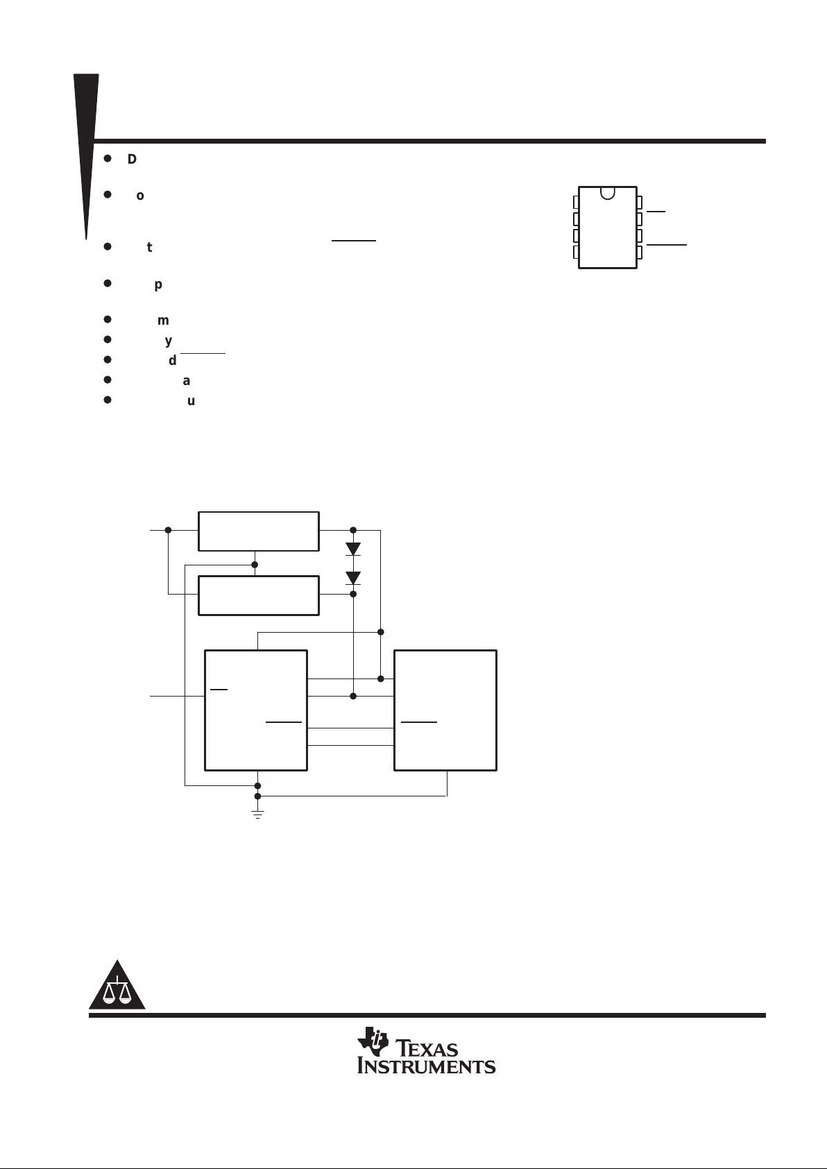
Figure 1 lists some of the typical applications for the TPS3305 family , and a schematic diagram for a DSP-based
system application. This application uses TI part numbers TPS3305–25, TPS7133, TPS71025, and
TMS320VC549.
TPS7133
V
O
V
I
GND
TPS71025
V
O
V
I
GND
V
DD
GND
SENSE 1
SENSE 2
MR
RESET
WDI
DSP
GND
DV
DD
CV
DD
TMS320VC549TPS3305–25
RESET
XF
2.5 V
3.3 V
5 V – 10 V
External
Reset
Source
Figure 1. Applications Using the TPS3305 Family
• Applications using DSPs, Microcontrollers
or Microprocessors
• Industrial Equipment
• Programmable Controls
• Automotive Systems
• Portable/Battery Powered Equipment
• Intelligent Instruments
• Wireless Communication Systems
• Notebook/Desktop Computers
description
The TPS3305 family is a series of micropower supply voltage supervisors designed for circuit initialization,
primarily in DSP and processor-based systems, which require two supply voltages.
The product spectrum of the TPS3305 is designed for monitoring two independent supply voltages of
3.3 V/1.8 V, 3.3 V/2.5 V or 3.3 V /5 V.
PRODUCTION DATA information is current as of publication date.
Products conform to specifications per the terms of Texas Instruments
standard warranty. Production processing does not necessarily include
testing of all parameters.
Copyright 1998, Texas Instruments Incorporated
Please be aware that an important notice concerning availability, standard warranty, and use in critical applications of
Texas Instruments semiconductor products and disclaimers thereto appears at the end of this data sheet.
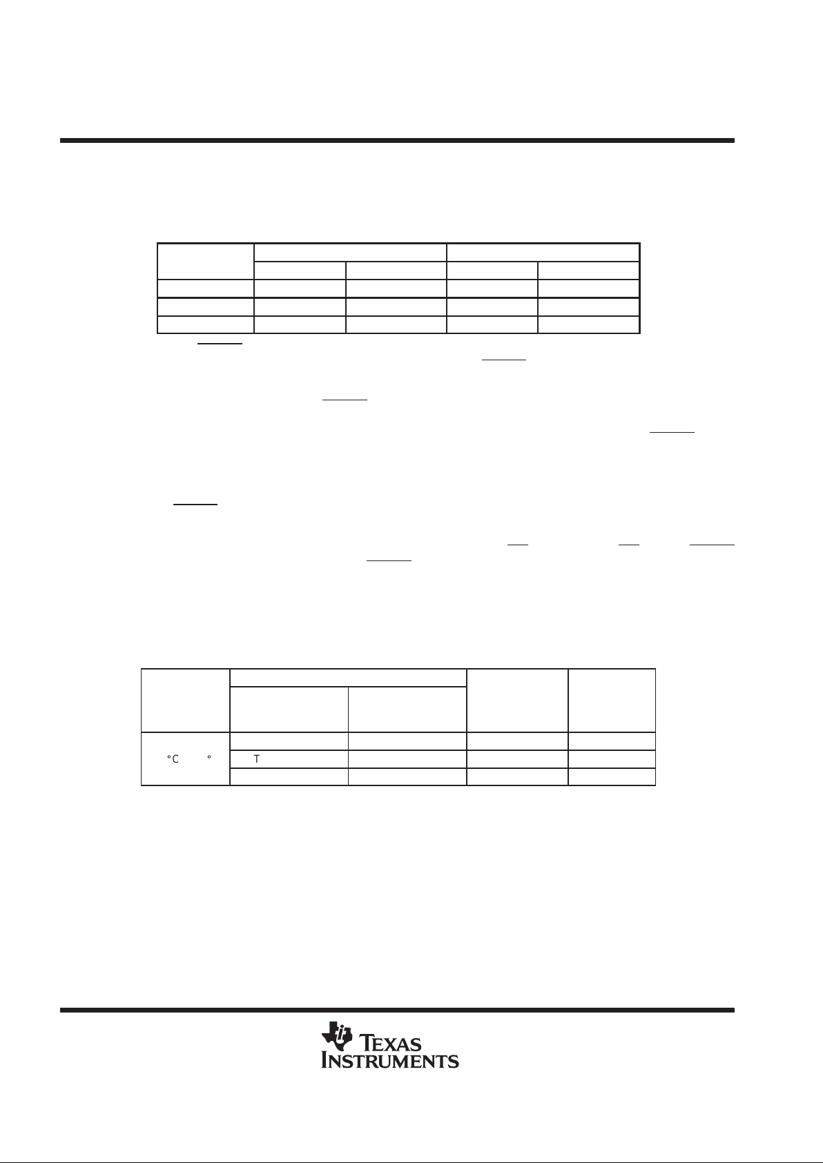
1
2
3
4
8
7
6
5
SENSE1
SENSE2
WDI
GND
V
DD
MR
RESET
RESET
D OR DGN PACKAGE
(TOP VIEW)
TPS3305-18, TPS3305-25, TPS3305-33
DUAL PROCESSOR SUPERVISORS
SLVS198 – DECEMBER 1998
2
POST OFFICE BOX 655303 • DALLAS, TEXAS 75265
description (continued)
The various supply voltage supervisors are designed to monitor the nominal supply voltage, as shown in the
following supply voltage monitoring table.
SUPPLY VOLTAGE MONITORING
NOMINAL SUPERVISED VOLTAGE THRESHOLD VOLTAGE (TYP)
DEVICE
SENSE1 SENSE2 SENSE1 SENSE2
TPS3305-18 3.3 V 1.8 V 2.93 V 1.68 V
TPS3305-25 3.3 V 2.5 V 2.93 V 2.25 V
TPS3305-33 5 V 3.3 V 4.55 V 2.93 V
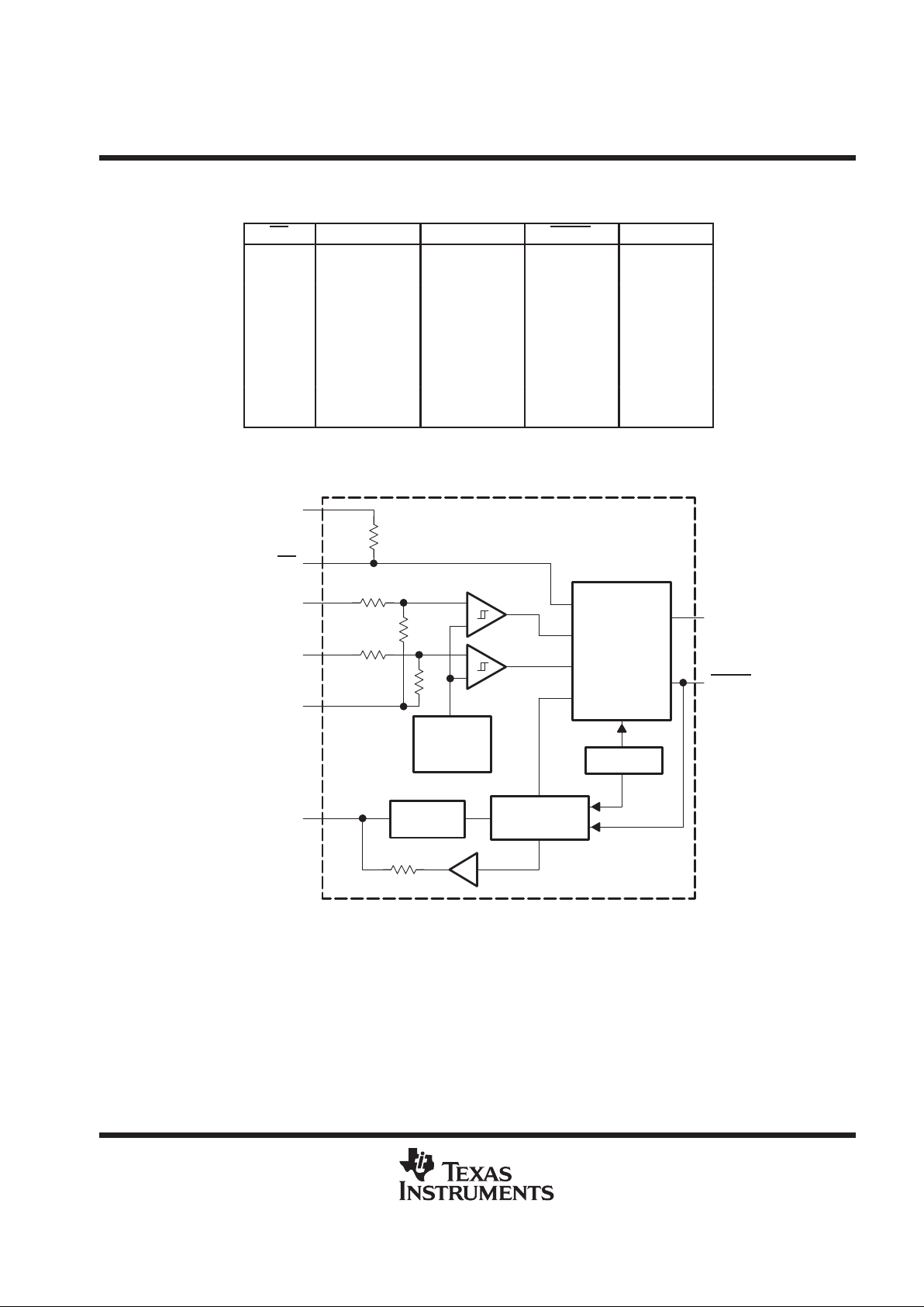
During power-on, RESET is asserted when the supply voltage V
DD
becomes higher than 1.1 V . Thereafter , the
supply voltage supervisor monitors the SENSEn inputs
and keeps RESET active as long as SENSEn remains
below the threshold voltage V
IT+
.
An internal timer delays the return of the RESET
output to the inactive state (high) to ensure proper system reset.
The delay time, t
d
typ
= 200 ms, starts after SENSE1 and SENSE2 inputs have risen above the threshold voltage
V
IT+
. When the voltage at SENSE1 or SENSE2 input drops below the threshold voltage V
IT–
, the RESET output
becomes active (low) again.
The TPS3305-xx devices integrate a watchdog timer that is periodically triggered by a positive or negative
transition of WDI. When the supervising system fails to retrigger the watchdog circuit within the time-out interval,
t
t(out)
= 1.6 s, RESET becomes active for the time period t
d
. This event also reinitializes the watchdog timer.
Leaving WDI unconnected disables the watchdog.
The TPS3305-xx family of devices incorporates a manual reset input, MR
. A low level at MR causes RESET
to become active. In addition to the active-low RESET output, the TPS3305-xx family includes an active-high
RESET output.
The TPS3305-xx devices are available in either 8-pin MSOP or standard 8-pin SO packages.
The TPS3305-xx family is characterized for operation over a temperature range of – 40°C to 85°C.
AVAILABLE OPTIONS
PACKAGED DEVICES
T
A
SMALL OUTLINE
(D)
PowerPAD
µ-SMALL OUTLINE
(DGN)
MARKING
DGN PACKAGE
CHIP FORM
(Y)
TPS3305-18D TPS3305-18DGN TIAAM TPS3305-18Y
–40
_
C to 85
_
C
TPS3305-25D TPS3305-25DGN TIAAN TPS3305-25Y
TPS3305-33D TPS3305-33DGN TIAAO TPS3305-33Y
PowerPAD is a trademark of Texas Instruments Incorporated.
TPS3305-18, TPS3305-25, TPS3305-33
DUAL PROCESSOR SUPERVISORS
SLVS198 – DECEMBER 1998
3
POST OFFICE BOX 655303 • DALLAS, TEXAS 75265
description (continued)
FUNCTION/TRUTH TABLES
MR
SENSE1>V
IT1
SENSE2>V
IT2
RESET RESET
L X
†
X
†
L H
H 0 0 L H
H 0 0 L H
H 0 1 L H
H 0 1 L H
H 1 0 L H
H 1 0 L H
H 1 1 L H
H 1 1 H L
†
X = Don’t care
functional block diagram
_
+
_
+
R4
R2
R1
R3
Reference
Voltage
of 1.25 V
RESET
Logic + Timer
Oscillator
14 kΩ
V
DD
MR
SENSE 1
SENSE 2
GND
WDI
RESET
RESET
TPS3305
Watchdog
Logic + Timer
40 kΩ
Transition
Detection
TPS3305-18, TPS3305-25, TPS3305-33
DUAL PROCESSOR SUPERVISORS
SLVS198 – DECEMBER 1998
4
POST OFFICE BOX 655303 • DALLAS, TEXAS 75265
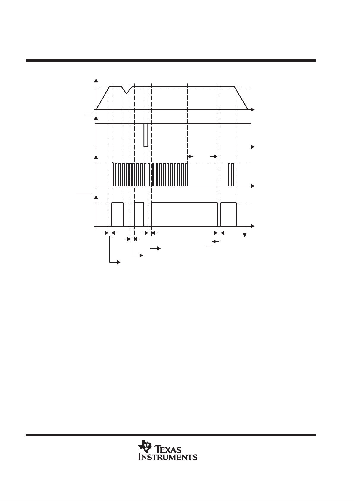
timing diagram
t
d
t
d
t
d
RESET Because of WDI
RESET Because of MR
RESET Because of SENSE Below V
IT–
RESET Because of SENSE Below V
IT–
SENSEn
V
(nom)
V
IT–
MR
1
0
1
0
RESET
t
t
t
1
0
WDI
t
t(out)
t
t
d
RESET Because
of SENSE Below V
IT–
 Loading...