


Texas Instruments TMX320VC549PGE-120, TMX320VC549GGU-120, TMS320VC549PGE-80, TMS320VC549PGE-100, TMS320VC549GGU-80 Datasheet
...C
F 2 A A C
SPRS078F ± SEPTEMBER 1998 ± REVISED MAY 2000
Advanced Multibus Architecture With Three Separate 16-Bit Data Memory Buses and One Program Memory Bus
40-Bit Arithmetic Logic Unit (ALU) Including a 40-Bit Barrel Shifter and Two Independent 40-Bit Accumulators
17- ×17-Bit Parallel Multiplier Coupled to a
40-Bit Dedicated Adder for Non-Pipelined Single-Cycle Multiply/Accumulate (MAC) Operation
Compare, Select, and Store Unit (CSSU) for the Add/Compare Selection of the Viterbi Operator
Exponent Encoder to Compute an Exponent Value of a 40-Bit Accumulator Value in a Single Cycle
Two Address Generators With Eight Auxiliary Registers and Two Auxiliary Register Arithmetic Units (ARAUs)
Data Bus With a Bus Holder Feature
Address Bus With a Bus Holder Feature
Extended Addressing Mode for 8M × 16-Bit
Maximum Addressable External Program Space
192K ×16-Bit Maximum Addressable
Memory Space (64K Words Program, 64K Words Data, and 64K Words I/O)
On-Chip ROM with Some Configurable to Program/Data Memory
Dual-Access On-Chip RAM
Single-Access On-Chip RAM
Single-Instruction Repeat and Block-Repeat Operations for Program Code
Block-Memory-Move Instructions for Better Program and Data Management
Instructions With a 32-Bit Long Word Operand
Instructions With Twoor Three-Operand Reads
Arithmetic Instructions With Parallel Store and Parallel Load
Conditional Store Instructions
Fast Return From Interrupt
On-Chip Peripherals
±Software-Programmable Wait-State Generator and Programmable Bank Switching
±On-Chip Phase-Locked Loop (PLL) Clock Generator With Internal Oscillator or External Clock Source
±Time-Division Multiplexed (TDM) Serial Port
±Buffered Serial Port (BSP)
±8-Bit Parallel Host Port Interface (HPI)
±One 16-Bit Timer
±External-Input/Output (XIO) Off Control to Disable the External Data Bus, Address Bus and Control Signals
Power Consumption Control With IDLE1, IDLE2, and IDLE3 Instructions With Power-Down Modes
CLKOUT Off Control to Disable CLKOUT
On-Chip Scan-Based Emulation Logic, IEEE Std 1149.1² (JTAG) Boundary Scan Logic
12.5-ns Single-Cycle Fixed-Point Instruction Execution Time (80 MIPS) for 3.3-V Power Supply)
10-ns Single-Cycle Fixed-Point Instruction Execution Time (100 MIPS) for 3.3-V Power Supply (2.5-V Core)
8.3-ns Single-Cycle Fixed-Point Instruction Execution Time (120 MIPS) for 3.3-V Power Supply (2.5-V Core) (Product Preview Data)
Available in a 144-Pin Plastic Thin Quad Flatpack (TQFP) (PGE Suffix) and a 144-Pin Ball Grid Array (BGA) (GGU Suffix)
NOTE: The data provided in this data sheet for the 8.3-ns, 120 MIPS device is considered to be Product Preview data as the devices have not completed reliability performance qualification testing according to TI Quality Systems Specifications.
Please be aware that an important notice concerning availability, standard warranty, and use in critical applications of Texas Instruments semiconductor products and disclaimers thereto appears at the end of this data sheet.
² IEEE Standard 1149.1-1990 Standard-Test-Access Port and Boundary Scan Architecture.
|
|
-$%, |
) .'!(- |
)(- %(, |
C |
Copyright 2000, Texas Instruments Incorporated |
|
A A %(")+' -%)( .++!(- , |
)" *. &% -%)( |
-! +) |
. -, )(")+' -) |
|
|||
,*! %"% -%)(, *!+ -$! |
-!+', |
)" !0 , (,-+.'!(-, ,- ( + |
/ ++ (-1 |
|
|||
+) . -%)( *+) !,,%(# |
)!, |
()- |
(! !,, +%&1 |
%( &. ! |
-!,-%(# |
)" && |
|
* + '!-!+, |
|
|
|
|
|
|
|
|
|
|
|
|
POST OFFICE BOX 1443 •HOUSTON, TEXAS 77251±1443 |
1 |
|

TMS320VC549
FIXED POINT DIGITAL SIGNAL PROCESSOR
SPRS078F ± SEPTEMBER 1998 ± REVISED MAY 2000
Table of Contents
Description . . . . . . . . . . . . . . . . . . . . . . . . . . . . . . . . . . . 2
Pin Assignments . . . . . . . . . . . . . . . . . . . . . . . . . . . . . . 6
Signal Descriptions . . . . . . . . . . . . . . . . . . . . . . . . . . . 7
Absolute Maximum Ratings . . . . . . . . . . . . . . . . . . . . 12
Recommended Operating Conditions . . . . . . . . . . . 12
Electrical Characteristics . . . . . . . . . . . . . . . . . . . . . . 13
Parameter Measurement Information . . . . . . . . . . . . 14
Timing Parameter Symbology . . . . . . . . . . . . . . . . . . 14
Signal Transition Reference Points . . . . . . . . . . . . . . 14
Internal Oscillator With External Crystal . . . . . . . . . 15
Divide-By-Two/Divide-By-Four Clock Option . . . . . 16
Multiply-By-N Clock Option . . . . . . . . . . . . . . . . . . . . 18
Memory and Parallel I/O Interface Timing . . . . . . . . 20 Timing Requirements for a Parallel I/O Port Read . 26 SPICE Simulation Results . . . . . . . . . . . . . . . . . . . . . 28 Ready Timing for Externally Generated Wait States 31 HOLD and HOLDA Timing . . . . . . . . . . . . . . . . . . . . . 36 Reset, BIO, Interrupt, and MP/MC Timings . . . . . . . 38 Serial Port Receive Timing . . . . . . . . . . . . . . . . . . . . . 42 Buffered Serial Port Receive Timing . . . . . . . . . . . . . 45 Serial-Port Receive Timing in TDM Mode . . . . . . . . 49 Host-Port Interface Timing . . . . . . . . . . . . . . . . . . . . . 53 Mechanical Data . . . . . . . . . . . . . . . . . . . . . . . . . . . . . 59
description
The TMS320VC549 fixed-point, digital signal processor (DSP) (hereafter referred to as the '549) is based on an advanced modified Harvard architecture that has one program memory bus and three data memory buses. The processor also provides an arithmetic logic unit (ALU) that has a high degree of parallelism, application-specific hardware logic, on-chip memory, and additional on-chip peripherals. The '549 also utilizes a highly specialized instruction set, which is the basis of its operational flexibility and speed.
Separate program and data spaces allow simultaneous access to program instructions and data, providing the high degree of parallelism. Two reads and one write operation can be performed in a single cycle. Instructions with parallel store and application-specific instructions can fully utilize this architecture. In addition, data can be transferred between data and program spaces. Such parallelism supports a powerful set of arithmetic, logic, and bit-manipulation operations that can all be performed in a single machine cycle. In addition, the '549 includes the control mechanisms to manage interrupts, repeated operations, and function calls.
This data sheet contains the pin layouts, signal descriptions, and electrical specifications for the TMS320VC549 DSP. For additional information, see the TMS320C54x, TMS320LC54x, TMS320VC54x Fixed-Point Digital Signal Processors data sheet (literature number SPRS039). The SPRS039 is considered a family functional overview and should be used in conjunction with this data sheet.
2 |
POST OFFICE BOX 1443 •HOUSTON, TEXAS 77251±1443 |

|
|
|
|
|
|
|
|
|
|
|
|
|
|
|
|
|
|
|
|
|
|
|
|
|
|
|
|
|
|
|
|
|
|
|
|
|
|
|
|
|
|
|
|
|
|
|
|
|
|
|
|
|
|
|
|
|
|
|
|
|
|
|
|
|
|
|
|
|
|
|
|
|
|
|
|
|
|
|
|
|
|
|
|
|
|
|
|
|
|
|
|
|
|
|
|
|
|
|
|
|
|
|
|
|
|
|
|
|
|
|
|
|
|
|
|
|
|
|
|
|
|
|
|
|
|
|
|
|
|
|
|
|
|
|
|
|
|
|
|
|
|
|
|
|
|
|
TMS320VC549 |
||||||
|
|
|
|
|
|
|
|
|
|
|
|
|
|
|
|
|
|
|
|
|
|
|
|
|
|
|
|
|
|
|
|
|
|
|
|
|
|
|
|
|
|
|
|
|
|
|
|
|
|
|
|
|
|
|
|
|
|
|
|
|
|
|
|
|
|
|
|
|
|
|
|
|
|
|
|
|
|
|
|
|
|
|
|
|
|
FIXED POINT |
DIGITAL |
|
|
|
SIGNAL PROCESSOR |
||||||||||||||||||||||||||||||||||||||||||||||||||||||||||||||
|
|
|
|
|
|
|
|
|
|
|
|
|
|
|
|
|
|
|
|
|
|
|
|
|
|
|
|
|
|
|
|
|
|
|
|
|
|
|
|
|
|
|
|
|
|
|
|
|
|
|
|
|
|
|
|
|
|
|
|
|
|
|
|
|
|
|
|
|
|
|
|
|
|
|
|
|
|
|
|
|
|
|
|
|
|
|
|
|
|
|
|
|
|
|
|
|
|
|
|
|
|
|
|
|
|
|
|
|
|
|
|
|
|
|
SPRS078F ± SEPTEMBER 1998 ± REVISED MAY 2000 |
||||||||||||||||||||||||||||||||||||||
|
|
|
|
|
|
|
|
|
|
|
|
|
|
|
|
|
|
|
|
|
|
|
|
|
|
|
|
|
|
|
|
|
|
|
|
|
|
|
|
|
|
|
|
|
|
|
|
|
|
|
|
|
|
|
|
|
|
|
|
|
|
|
|
|
|
|
|
|
|
|
|
|
|
|
|
|
|
|
|
|
|
|
|
|
|
|
|
|
|
|
|
|
|
|
|
|
|
|
|
|
|
|
|
|
|
|
|
|
|
|
|
|
|
|
|
|
|
|
|
|
|
|
|
|
|
|
|
|
|
|
|
|
|
|
|
|
|
|
|
|
|
|
|
|
|
|
|
|
|
|
|
|
|
|
|
|
|
|
|
|
|
|
|
|
|
|
|
|
|
|
|
|
|
|
|
|
|
|
|
|
|
|
|
|
|
|
|
|
|
|
|
|
|
|
|
|
|
|
|
|
|
|
|
|
|
|
|
|
|
|
|
|
|
|
|
|
|
|
|
|
|
|
PGE PACKAGE²³ |
|
|
|
|
|
|
|
|
|
|
|
|
|
|
|
|
|
|
|
|
|
|
|
|
|
|
|
|
|
|
|
|
|
|
|
|
|
|
|
|
|
|
|
|
|
|
|
|
|
|
|
|
|
|||||||||||||||||||||||||||||||
|
|
|
|
|
|
|
|
|
|
|
|
|
|
|
|
|
|
|
|
|
|
|
|
|
|
|
|
|
|
|
|
|
|
|
|
|
|
|
|
|
|
|
|
|
|
|
|
|
|
|
|
|
|
|
|
|
|
|
|
|
|
|
|
|
|
|
|
|
|
|
|
|
(TOP VIEW) |
|
|
|
|
|
|
|
|
|
|
|
|
|
|
|
|
|
|
|
|
|
|
|
|
|
|
|
|
|
|
|
|
|
|
|
|
|
|
|
|
|
|
|
|
|
|
|
|
|
|
|
|
|
|
|
|
|
|
|
|
|
|||||||||||||||||||
|
|
|
|
|
|
|
|
|
|
|
|
|
|
|
DD |
|
|
|
|
|
|
|
|
|
|
|
|
|
|
|
|
|
|
|
|
|
|
|
|
|
|
|
|
|
|
|
|
|
|
|
|
|
|
|
|
|
|
|
|
|
|
|
DD |
|
HDS2 |
|
|
|
HDS1 |
|
|
|
DD |
|
|
|
|
|
|
|
|
|
|
|
|
|
|
|
|
|
|
|
|
|
|
|
|
|
|
|
|
|
|
|
|
|
|
|
|
|
|
|
|
|
|
|
DD |
|
|
|
|
|
|
|
|
|
|
|
|
|
|
|
|
|
|||||||||||||||||||
|
|
|
|
|
|
|
|
|
SS |
|
A21 |
|
|
A9 |
|
|
A8 |
|
A7 |
|
A6 |
|
A5 |
|
|
A4 |
|
HD6 |
|
A3 |
|
A2 |
|
|
A1 |
|
|
A0 |
|
|
|
|
SS |
|
SS |
|
|
HD5 |
|
D15 |
|
D14 |
|
D13 |
HD4 |
|
D12 |
D11 |
|
D10 |
D9 |
D8 |
D7 |
|
D6 |
|
|
SS |
|
A20 |
|
|
|
A19 |
|
|
|
|
|
|
|
||||||||||||||||||||||||||||||||||||||||||||||||||||||||||||||||||||||||
|
|
|
|
|
|
|
|
V |
|
|
CV |
|
|
|
|
|
|
|
|
|
|
|
|
|
|
|
|
DV |
|
V |
|
V |
|
CV |
|
|
|
|
|
|
|
|
DV |
|
V |
|
|
|
|
|
|
|
|
|
|
|
|||||||||||||||||||||||||||||||||||||||||||||||||||||||||||||||||||||||||||||||||||||||||||||||||
|
|
|
|
|
|
|
|
|
|
|
|
|
|
|
|
|
|
|
|
|
|
|
|
|
|
|
|
|
|
|
|
|
|
|
|
|
|
|
|
|
|
|
|
|
|
|
|
|
|
|
|
|
|
|
|
|
|
|
|
|
|
|
|
|
|
|
|
|
|
|
|
|
|
|
|
|
|
|
|
|
|
|
|
|
|
|
|
|
|
|
|
|
|
|
|
|
|
|
|
|
|
|
|
|
|
|
|
|
|
|
|
|
|
|
|
|
|
|
|
|
|
|
|
|
|
|
|
|
|
|
|
|
|
|
|
|
|
|
|
|
|
|
|
|
|
|
|
|
|
|
|
|
|
|
|
VSS |
|
144 |
|
143 |
|
142 |
|
141 |
|
140 |
|
139 |
|
138 |
|
137 |
|
136 |
|
135 |
|
134 |
|
133 |
|
132 |
131 |
130 |
129 |
|
128 |
|
127 |
|
126 |
|
125 |
|
124 |
|
123 |
|
122 |
|
121 |
|
120 |
|
119 |
|
118 |
117 |
|
116 |
|
115 |
|
114 |
|
113 |
|
112 |
|
111 |
|
|
110 |
109 |
|
|
|
|
A18 |
||||||||||||||||||||||||||||||||||||||||||||||||||||||||||||||||||||||||||||||
|
|
|
|
|
|||||||||||||||||||||||||||||||||||||||||||||||||||||||||||||||||||||||||||||||||||||||||||||||||||||||||||||||||||||||||||||||||||||||||||||||||||||
|
|
|
1 |
|
|
|
|
|
|
|
|
|
|
|
|
|
|
|
|
|
|
|
|
|
|
|
|
|
|
|
|
|
|
|
|
|
|
|
|
|
|
|
|
|
|
|
|
|
|
|
|
|
|
|
|
|
|
|
|
|
|
|
|
|
|
|
|
|
|
|
|
|
|
|
|
|
|
|
|
|
|
|
|
|
|
|
|
|
|
|
|
|
|
|
|
|
|
|
|
|
|
|
|
|
|
|
|
|
|
|
|
|
|
|
|
|
|
|
|
|
|
|
|
|
|
|
|
|
|
|
|
|
|
|
|
|
|
|
108 |
|
|
||||||||||||
|
|
|
|
|
|
|
|
|
|
|
|
|
|
|
|
|
|
|
|
|
|
|
|
|
|
|
|
|
|
|
|
|
|
|
|
|
|
|
|
|
|
|
|
|
|
|
|
|
|
|
|
|
|
|
|
|
|
|
|
|
|
|
|
|
|
|
|
|
|
|
|
|
|
|
|
|
|
|
|
|
|
|
|
|
|
|
|
|
|
|
|
|
|
|
|
|
|
|
|
|
|
|
|
|
|
|
|
|
|
|
|
|
|
|
|
|
|
|
|
|
|
|
|
|
|
|
|
|
|
|
|
|
|
|
|
|
|
|
|
||||||||||||||
|
|
A22 |
|
2 |
|
|
|
|
|
|
|
|
|
|
|
|
|
|
|
|
|
|
|
|
|
|
|
|
|
|
|
|
|
|
|
|
|
|
|
|
|
|
|
|
|
|
|
|
|
|
|
|
|
|
|
|
|
|
|
|
|
|
|
|
|
|
|
|
|
|
|
|
|
|
|
|
|
|
|
|
|
|
|
|
|
|
|
|
|
|
|
|
|
|
|
|
|
|
|
|
|
|
|
|
|
|
|
|
|
|
|
|
|
|
|
|
|
|
|
|
|
|
|
|
|
|
|
|
|
|
|
|
|
|
|
|
|
|
|
107 |
|
|
A17 |
||||||||||
|
|
VSS |
|
3 |
|
|
|
|
|
|
|
|
|
|
|
|
|
|
|
|
|
|
|
|
|
|
|
|
|
|
|
|
|
|
|
|
|
|
|
|
|
|
|
|
|
|
|
|
|
|
|
|
|
|
|
|
|
|
|
|
|
|
|
|
|
|
|
|
|
|
|
|
|
|
|
|
|
|
|
|
|
|
|
|
|
|
|
|
|
|
|
|
|
|
|
|
|
|
|
|
|
|
|
|
|
|
|
|
|
|
|
|
|
|
|
|
|
|
|
|
|
|
|
|
|
|
|
|
|
|
|
|
|
|
|
|
|
|
|
106 |
|
|
VSS |
||||||||||
|
|
|
|
|
|
|
|
|
|
|
|
|
|
|
|
|
|
|
|
|
|
|
|
|
|
|
|
|
|
|
|
|
|
|
|
|
|
|
|
|
|
|
|
|
|
|
|
|
|
|
|
|
|
|
|
|
|
|
|
|
|
|
|
|
|
|
|
|
|
|
|
|
|
|
|
|
|
|
|
|
|
|
|
|
|
|
|
|
|
|
|
|
|
|
|
|
|
|
|
|
|
|
|
|
|
|
|
|
|
|
|
|
|
|
|
|
|
|
|
|
|
|
|
|
|
|
|
|
|
|
|
|
|
|
|
|
|
|
|
||||||||||||||
|
DVDD |
|
4 |
|
|
|
|
|
|
|
|
|
|
|
|
|
|
|
|
|
|
|
|
|
|
|
|
|
|
|
|
|
|
|
|
|
|
|
|
|
|
|
|
|
|
|
|
|
|
|
|
|
|
|
|
|
|
|
|
|
|
|
|
|
|
|
|
|
|
|
|
|
|
|
|
|
|
|
|
|
|
|
|
|
|
|
|
|
|
|
|
|
|
|
|
|
|
|
|
|
|
|
|
|
|
|
|
|
|
|
|
|
|
|
|
|
|
|
|
|
|
|
|
|
|
|
|
|
|
|
|
|
|
|
|
|
|
|
105 |
|
|
A16 |
|||||||||||
|
|
A10 |
|
5 |
|
|
|
|
|
|
|
|
|
|
|
|
|
|
|
|
|
|
|
|
|
|
|
|
|
|
|
|
|
|
|
|
|
|
|
|
|
|
|
|
|
|
|
|
|
|
|
|
|
|
|
|
|
|
|
|
|
|
|
|
|
|
|
|
|
|
|
|
|
|
|
|
|
|
|
|
|
|
|
|
|
|
|
|
|
|
|
|
|
|
|
|
|
|
|
|
|
|
|
|
|
|
|
|
|
|
|
|
|
|
|
|
|
|
|
|
|
|
|
|
|
|
|
|
|
|
|
|
|
|
|
|
|
|
|
104 |
|
|
D5 |
||||||||||
|
|
HD7 |
|
6 |
|
|
|
|
|
|
|
|
|
|
|
|
|
|
|
|
|
|
|
|
|
|
|
|
|
|
|
|
|
|
|
|
|
|
|
|
|
|
|
|
|
|
|
|
|
|
|
|
|
|
|
|
|
|
|
|
|
|
|
|
|
|
|
|
|
|
|
|
|
|
|
|
|
|
|
|
|
|
|
|
|
|
|
|
|
|
|
|
|
|
|
|
|
|
|
|
|
|
|
|
|
|
|
|
|
|
|
|
|
|
|
|
|
|
|
|
|
|
|
|
|
|
|
|
|
|
|
|
|
|
|
|
|
|
|
103 |
|
|
D4 |
||||||||||
|
|
|
|
|
|
|
|
|
|
|
|
|
|
|
|
|
|
|
|
|
|
|
|
|
|
|
|
|
|
|
|
|
|
|
|
|
|
|
|
|
|
|
|
|
|
|
|
|
|
|
|
|
|
|
|
|
|
|
|
|
|
|
|
|
|
|
|
|
|
|
|
|
|
|
|
|
|
|
|
|
|
|
|
|
|
|
|
|
|
|
|
|
|
|
|
|
|
|
|
|
|
|
|
|
|
|
|
|
|
|
|
|
|
|
|
|
|
|
|
|
|
|
|
|
|
|
|
|
|
|
|
|
|
|
|
|
|
|
|
||||||||||||||
|
|
A11 |
|
7 |
|
|
|
|
|
|
|
|
|
|
|
|
|
|
|
|
|
|
|
|
|
|
|
|
|
|
|
|
|
|
|
|
|
|
|
|
|
|
|
|
|
|
|
|
|
|
|
|
|
|
|
|
|
|
|
|
|
|
|
|
|
|
|
|
|
|
|
|
|
|
|
|
|
|
|
|
|
|
|
|
|
|
|
|
|
|
|
|
|
|
|
|
|
|
|
|
|
|
|
|
|
|
|
|
|
|
|
|
|
|
|
|
|
|
|
|
|
|
|
|
|
|
|
|
|
|
|
|
|
|
|
|
|
|
|
102 |
|
|
D3 |
||||||||||
|
|
|
|
|
|
|
|
|
|
|
|
|
|
|
|
|
|
|
|
|
|
|
|
|
|
|
|
|
|
|
|
|
|
|
|
|
|
|
|
|
|
|
|
|
|
|
|
|
|
|
|
|
|
|
|
|
|
|
|
|
|
|
|
|
|
|
|
|
|
|
|
|
|
|
|
|
|
|
|
|
|
|
|
|
|
|
|
|
|
|
|
|
|
|
|
|
|
|
|
|
|
|
|
|
|
|
|
|
|
|
|
|
|
|
|
|
|
|
|
|
|
|
|
|
|
|
|
|
|
|
|
|
|
|
|
|
|
|
|
||||||||||||||
|
|
A12 |
|
8 |
|
|
|
|
|
|
|
|
|
|
|
|
|
|
|
|
|
|
|
|
|
|
|
|
|
|
|
|
|
|
|
|
|
|
|
|
|
|
|
|
|
|
|
|
|
|
|
|
|
|
|
|
|
|
|
|
|
|
|
|
|
|
|
|
|
|
|
|
|
|
|
|
|
|
|
|
|
|
|
|
|
|
|
|
|
|
|
|
|
|
|
|
|
|
|
|
|
|
|
|
|
|
|
|
|
|
|
|
|
|
|
|
|
|
|
|
|
|
|
|
|
|
|
|
|
|
|
|
|
|
|
|
|
|
|
101 |
|
|
D2 |
||||||||||
|
|
|
|
|
|
|
|
|
|
|
|
|
|
|
|
|
|
|
|
|
|
|
|
|
|
|
|
|
|
|
|
|
|
|
|
|
|
|
|
|
|
|
|
|
|
|
|
|
|
|
|
|
|
|
|
|
|
|
|
|
|
|
|
|
|
|
|
|
|
|
|
|
|
|
|
|
|
|
|
|
|
|
|
|
|
|
|
|
|
|
|
|
|
|
|
|
|
|
|
|
|
|
|
|
|
|
|
|
|
|
|
|
|
|
|
|
|
|
|
|
|
|
|
|
|
|
|
|
|
|
|
|
|
|
|
|
|
|
|
||||||||||||||
|
|
A13 |
|
9 |
|
|
|
|
|
|
|
|
|
|
|
|
|
|
|
|
|
|
|
|
|
|
|
|
|
|
|
|
|
|
|
|
|
|
|
|
|
|
|
|
|
|
|
|
|
|
|
|
|
|
|
|
|
|
|
|
|
|
|
|
|
|
|
|
|
|
|
|
|
|
|
|
|
|
|
|
|
|
|
|
|
|
|
|
|
|
|
|
|
|
|
|
|
|
|
|
|
|
|
|
|
|
|
|
|
|
|
|
|
|
|
|
|
|
|
|
|
|
|
|
|
|
|
|
|
|
|
|
|
|
|
|
|
|
|
100 |
|
|
D1 |
||||||||||
|
|
|
|
|
|
|
|
|
|
|
|
|
|
|
|
|
|
|
|
|
|
|
|
|
|
|
|
|
|
|
|
|
|
|
|
|
|
|
|
|
|
|
|
|
|
|
|
|
|
|
|
|
|
|
|
|
|
|
|
|
|
|
|
|
|
|
|
|
|
|
|
|
|
|
|
|
|
|
|
|
|
|
|
|
|
|
|
|
|
|
|
|
|
|
|
|
|
|
|
|
|
|
|
|
|
|
|
|
|
|
|
|
|
|
|
|
|
|
|
|
|
|
|
|
|
|
|
|
|
|
|
|
|
|
|
|
|
|
|
||||||||||||||
|
|
A14 |
|
10 |
|
|
|
|
|
|
|
|
|
|
|
|
|
|
|
|
|
|
|
|
|
|
|
|
|
|
|
|
|
|
|
|
|
|
|
|
|
|
|
|
|
|
|
|
|
|
|
|
|
|
|
|
|
|
|
|
|
|
|
|
|
|
|
|
|
|
|
|
|
|
|
|
|
|
|
|
|
|
|
|
|
|
|
|
|
|
|
|
|
|
|
|
|
|
|
|
|
|
|
|
|
|
|
|
|
|
|
|
|
|
|
|
|
|
|
|
|
|
|
|
|
|
|
|
|
|
|
|
|
|
|
|
|
|
99 |
|
|
D0 |
|||||||||||
|
|
|
|
|
|
|
|
|
|
|
|
|
|
|
|
|
|
|
|
|
|
|
|
|
|
|
|
|
|
|
|
|
|
|
|
|
|
|
|
|
|
|
|
|
|
|
|
|
|
|
|
|
|
|
|
|
|
|
|
|
|
|
|
|
|
|
|
|
|
|
|
|
|
|
|
|
|
|
|
|
|
|
|
|
|
|
|
|
|
|
|
|
|
|
|
|
|
|
|
|
|
|
|
|
|
|
|
|
|
|
|
|
|
|
|
|
|
|
|
|
|
|
|
|
|
|
|
|
|
|
|
|
|
|
|
|
|
|
|||||||||||||||
|
|
A15 |
|
11 |
|
|
|
|
|
|
|
|
|
|
|
|
|
|
|
|
|
|
|
|
|
|
|
|
|
|
|
|
|
|
|
|
|
|
|
|
|
|
|
|
|
|
|
|
|
|
|
|
|
|
|
|
|
|
|
|
|
|
|
|
|
|
|
|
|
|
|
|
|
|
|
|
|
|
|
|
|
|
|
|
|
|
|
|
|
|
|
|
|
|
|
|
|
|
|
|
|
|
|
|
|
|
|
|
|
|
|
|
|
|
|
|
|
|
|
|
|
|
|
|
|
|
|
|
|
|
|
|
|
|
|
|
|
|
98 |
|
|
RS |
|||||||||||
|
|
|
|
|
|
|
|
|
|
|
|
|
|
|
|
|
|
|
|
|
|
|
|
|
|
|
|
|
|
|
|
|
|
|
|
|
|
|
|
|
|
|
|
|
|
|
|
|
|
|
|
|
|
|
|
|
|
|
|
|
|
|
|
|
|
|
|
|
|
|
|
|
|
|
|
|
|
|
|
|
|
|
|
|
|
|
|
|
|
|
|
|
|
|
|
|
|
|
|
|
|
|
|
|
|
|
|
|
|
|
|
|
|
|
|
|
|
|
|
|
|
|
|
|
|
|
|
|
|
|
|
|
|
|
|
|
|
|
|||||||||||||||
|
CVDD |
|
12 |
|
|
|
|
|
|
|
|
|
|
|
|
|
|
|
|
|
|
|
|
|
|
|
|
|
|
|
|
|
|
|
|
|
|
|
|
|
|
|
|
|
|
|
|
|
|
|
|
|
|
|
|
|
|
|
|
|
|
|
|
|
|
|
|
|
|
|
|
|
|
|
|
|
|
|
|
|
|
|
|
|
|
|
|
|
|
|
|
|
|
|
|
|
|
|
|
|
|
|
|
|
|
|
|
|
|
|
|
|
|
|
|
|
|
|
|
|
|
|
|
|
|
|
|
|
|
|
|
|
|
|
|
|
|
97 |
|
|
X2/CLKIN |
||||||||||||
|
|
|
|
|
|
|
|
|
|
|
|
|
|
|
|
|
|
|
|
|
|
|
|
|
|
|
|
|
|
|
|
|
|
|
|
|
|
|
|
|
|
|
|
|
|
|
|
|
|
|
|
|
|
|
|
|
|
|
|
|
|
|
|
|
|
|
|
|
|
|
|
|
|
|
|
|
|
|
|
|
|
|
|
|
|
|
|
|
|
|
|
|
|
|
|
|
|
|
|
|
|
|
|
|
|
|
|
|
|
|
|
|
|
|
|
|
|
|
|
|
|
|
|
|
|
|
|
|
|
|
|
|
|
|
|
|
|
||||||||||||||||
|
|
HAS |
|
13 |
|
|
|
|
|
|
|
|
|
|
|
|
|
|
|
|
|
|
|
|
|
|
|
|
|
|
|
|
|
|
|
|
|
|
|
|
|
|
|
|
|
|
|
|
|
|
|
|
|
|
|
|
|
|
|
|
|
|
|
|
|
|
|
|
|
|
|
|
|
|
|
|
|
|
|
|
|
|
|
|
|
|
|
|
|
|
|
|
|
|
|
|
|
|
|
|
|
|
|
|
|
|
|
|
|
|
|
|
|
|
|
|
|
|
|
|
|
|
|
|
|
|
|
|
|
|
|
|
|
|
|
|
|
|
96 |
|
|
X1 |
|||||||||||
|
|
VSS |
|
14 |
|
|
|
|
|
|
|
|
|
|
|
|
|
|
|
|
|
|
|
|
|
|
|
|
|
|
|
|
|
|
|
|
|
|
|
|
|
|
|
|
|
|
|
|
|
|
|
|
|
|
|
|
|
|
|
|
|
|
|
|
|
|
|
|
|
|
|
|
|
|
|
|
|
|
|
|
|
|
|
|
|
|
|
|
|
|
|
|
|
|
|
|
|
|
|
|
|
|
|
|
|
|
|
|
|
|
|
|
|
|
|
|
|
|
|
|
|
|
|
|
|
|
|
|
|
|
|
|
|
|
|
|
|
|
95 |
|
|
HD3 |
|||||||||||
|
|
|
|
|
|
|
|
|
|
|
|
|
|
|
|
|
|
|
|
|
|
|
|
|
|
|
|
|
|
|
|
|
|
|
|
|
|
|
|
|
|
|
|
|
|
|
|
|
|
|
|
|
|
|
|
|
|
|
|
|
|
|
|
|
|
|
|
|
|
|
|
|
|
|
|
|
|
|
|
|
|
|
|
|
|
|
|
|
|
|
|
|
|
|
|
|
|
|
|
|
|
|
|
|
|
|
|
|
|
|
|
|
|
|
|
|
|
|
|
|
|
|
|
|
|
|
|
|
|
|
|
|
|
|
|
|
|
|
|||||||||||||||
|
|
|
|
|
|
|
|
|
|
|
|
|
|
|
|
|
|
|
|
|
|
|
|
|
|
|
|
|
|
|
|
|
|
|
|
|
|
|
|
|
|
|
|
|
|
|
|
|
|
|
|
|
|
|
|
|
|
|
|
|
|
|
|
|
|
|
|
|
|
|
|
|
|
|
|
|
|
|
|
|
|
|
|
|
|
|
|
|
|
|
|
|
|
|
|
|
|
|
|
|
|
|
|
|
|
|
|
|
|
|
|
|
|
|
|
|
|
|
|
|
|
|
|
|
|
|
|
|
|
|
|
|
|
|
|
|
|
|
|||||||||||||||
|
|
VSS |
|
15 |
|
|
|
|
|
|
|
|
|
|
|
|
|
|
|
|
|
|
|
|
|
|
|
|
|
|
|
|
|
|
|
|
|
|
|
|
|
|
|
|
|
|
|
|
|
|
|
|
|
|
|
|
|
|
|
|
|
|
|
|
|
|
|
|
|
|
|
|
|
|
|
|
|
|
|
|
|
|
|
|
|
|
|
|
|
|
|
|
|
|
|
|
|
|
|
|
|
|
|
|
|
|
|
|
|
|
|
|
|
|
|
|
|
|
|
|
|
|
|
|
|
|
|
|
|
|
|
|
|
|
|
|
|
|
94 |
|
|
CLKOUT |
|||||||||||
|
CVDD |
|
16 |
|
|
|
|
|
|
|
|
|
|
|
|
|
|
|
|
|
|
|
|
|
|
|
|
|
|
|
|
|
|
|
|
|
|
|
|
|
|
|
|
|
|
|
|
|
|
|
|
|
|
|
|
|
|
|
|
|
|
|
|
|
|
|
|
|
|
|
|
|
|
|
|
|
|
|
|
|
|
|
|
|
|
|
|
|
|
|
|
|
|
|
|
|
|
|
|
|
|
|
|
|
|
|
|
|
|
|
|
|
|
|
|
|
|
|
|
|
|
|
|
|
|
|
|
|
|
|
|
|
|
|
|
|
|
93 |
|
|
VSS |
||||||||||||
|
|
HCS |
|
17 |
|
|
|
|
|
|
|
|
|
|
|
|
|
|
|
|
|
|
|
|
|
|
|
|
|
|
|
|
|
|
|
|
|
|
|
|
|
|
|
|
|
|
|
|
|
|
|
|
|
|
|
|
|
|
|
|
|
|
|
|
|
|
|
|
|
|
|
|
|
|
|
|
|
|
|
|
|
|
|
|
|
|
|
|
|
|
|
|
|
|
|
|
|
|
|
|
|
|
|
|
|
|
|
|
|
|
|
|
|
|
|
|
|
|
|
|
|
|
|
|
|
|
|
|
|
|
|
|
|
|
|
|
|
|
92 |
|
|
HPIENA |
|||||||||||
|
|
HR/W |
|
18 |
|
|
|
|
|
|
|
|
|
|
|
|
|
|
|
|
|
|
|
|
|
|
|
|
|
|
|
|
|
|
|
|
|
|
|
|
|
|
|
|
|
|
|
|
|
|
|
|
|
|
|
|
|
|
|
|
|
|
|
|
|
|
|
|
|
|
|
|
|
|
|
|
|
|
|
|
|
|
|
|
|
|
|
|
|
|
|
|
|
|
|
|
|
|
|
|
|
|
|
|
|
|
|
|
|
|
|
|
|
|
|
|
|
|
|
|
|
|
|
|
|
|
|
|
|
|
|
|
|
|
|
|
|
|
91 |
|
|
CVDD |
|||||||||||
|
|
|
|
|
|
|
|
|
|
|
|
|
|
|
|
|
|
|
|
|
|
|
|
|
|
|
|
|
|
|
|
|
|
|
|
|
|
|
|
|
|
|
|
|
|
|
|
|
|
|
|
|
|
|
|
|
|
|
|
|
|
|
|
|
|
|
|
|
|
|
|
|
|
|
|
|
|
|
|
|
|
|
|
|
|
|
|
|
|
|
|
|
|
|
|
|
|
|
|
|
|
|
|
|
|
|
|
|
|
|
|
|
|
|
|
|
|
|
|
|
|
|
|
|
|
|
|
|
|
|
|
|
|
|
|
|
|
|
|||||||||||||||
|
READY |
|
19 |
|
|
|
|
|
|
|
|
|
|
|
|
|
|
|
|
|
|
|
|
|
|
|
|
|
|
|
|
|
|
|
|
|
|
|
|
|
|
|
|
|
|
|
|
|
|
|
|
|
|
|
|
|
|
|
|
|
|
|
|
|
|
|
|
|
|
|
|
|
|
|
|
|
|
|
|
|
|
|
|
|
|
|
|
|
|
|
|
|
|
|
|
|
|
|
|
|
|
|
|
|
|
|
|
|
|
|
|
|
|
|
|
|
|
|
|
|
|
|
|
|
|
|
|
|
|
|
|
|
|
|
|
|
|
90 |
|
|
VSS |
||||||||||||
|
|
PS |
|
20 |
|
|
|
|
|
|
|
|
|
|
|
|
|
|
|
|
|
|
|
|
|
|
|
|
|
|
|
|
|
|
|
|
|
|
|
|
|
|
|
|
|
|
|
|
|
|
|
|
|
|
|
|
|
|
|
|
|
|
|
|
|
|
|
|
|
|
|
|
|
|
|
|
|
|
|
|
|
|
|
|
|
|
|
|
|
|
|
|
|
|
|
|
|
|
|
|
|
|
|
|
|
|
|
|
|
|
|
|
|
|
|
|
|
|
|
|
|
|
|
|
|
|
|
|
|
|
|
|
|
|
|
|
|
|
89 |
|
|
TMS |
|||||||||||
|
|
DS |
|
21 |
|
|
|
|
|
|
|
|
|
|
|
|
|
|
|
|
|
|
|
|
|
|
|
|
|
|
|
|
|
|
|
|
|
|
|
|
|
|
|
|
|
|
|
|
|
|
|
|
|
|
|
|
|
|
|
|
|
|
|
|
|
|
|
|
|
|
|
|
|
|
|
|
|
|
|
|
|
|
|
|
|
|
|
|
|
|
|
|
|
|
|
|
|
|
|
|
|
|
|
|
|
|
|
|
|
|
|
|
|
|
|
|
|
|
|
|
|
|
|
|
|
|
|
|
|
|
|
|
|
|
|
|
|
|
88 |
|
|
TCK |
|||||||||||
|
|
|
|
|
|
|
|
|
|
|
|
|
|
|
|
|
|
|
|
|
|
|
|
|
|
|
|
|
|
|
|
|
|
|
|
|
|
|
|
|
|
|
|
|
|
|
|
|
|
|
|
|
|
|
|
|
|
|
|
|
|
|
|
|
|
|
|
|
|
|
|
|
|
|
|
|
|
|
|
|
|
|
|
|
|
|
|
|
|
|
|
|
|
|
|
|
|
|
|
|
|
|
|
|
|
|
|
|
|
|
|
|
|
|
|
|
|
|
|
|
|
|
|
|
|
|
|
|
|
|
|
|
|
|
|
|
|
|
|||||||||||||||
|
|
IS |
|
22 |
|
|
|
|
|
|
|
|
|
|
|
|
|
|
|
|
|
|
|
|
|
|
|
|
|
|
|
|
|
|
|
|
|
|
|
|
|
|
|
|
|
|
|
|
|
|
|
|
|
|
|
|
|
|
|
|
|
|
|
|
|
|
|
|
|
|
|
|
|
|
|
|
|
|
|
|
|
|
|
|
|
|
|
|
|
|
|
|
|
|
|
|
|
|
|
|
|
|
|
|
|
|
|
|
|
|
|
|
|
|
|
|
|
|
|
|
|
|
|
|
|
|
|
|
|
|
|
|
|
|
|
|
|
|
87 |
|
|
TRST |
|
|
|
||||||||
|
|
|
|
|
|
|
|
|
|
|
|
|
|
|
|
|
|
|
|
|
|
|
|
|
|
|
|
|
|
|
|
|
|
|
|
|
|
|
|
|
|
|
|
|
|
|
|
|
|
|
|
|
|
|
|
|
|
|
|
|
|
|
|
|
|
|
|
|
|
|
|
|
|
|
|
|
|
|
|
|
|
|
|
|
|
|
|
|
|
|
|
|
|
|
|
|
|
|
|
|
|
|
|
|
|
|
|
|
|
|
|
|
|
|
|
|
|
|
|
|
|
|
|
|
|
|
|
|
|
|
|
|
|
|
|
|
|
|
|
|
|
|
|||||||||||
|
|
R/W |
|
23 |
|
|
|
|
|
|
|
|
|
|
|
|
|
|
|
|
|
|
|
|
|
|
|
|
|
|
|
|
|
|
|
|
|
|
|
|
|
|
|
|
|
|
|
|
|
|
|
|
|
|
|
|
|
|
|
|
|
|
|
|
|
|
|
|
|
|
|
|
|
|
|
|
|
|
|
|
|
|
|
|
|
|
|
|
|
|
|
|
|
|
|
|
|
|
|
|
|
|
|
|
|
|
|
|
|
|
|
|
|
|
|
|
|
|
|
|
|
|
|
|
|
|
|
|
|
|
|
|
|
|
|
|
|
|
86 |
|
|
TDI |
|||||||||||
|
|
|
|
|
|
|
|
|
|
|
|
|
|
|
|
|
|
|
|
|
|
|
|
|
|
|
|
|
|
|
|
|
|
|
|
|
|
|
|
|
|
|
|
|
|
|
|
|
|
|
|
|
|
|
|
|
|
|
|
|
|
|
|
|
|
|
|
|
|
|
|
|
|
|
|
|
|
|
|
|
|
|
|
|
|
|
|
|
|
|
|
|
|
|
|
|
|
|
|
|
|
|
|
|
|
|
|
|
|
|
|
|
|
|
|
|
|
|
|
|
|
|
|
|
|
|
|
|
|
|
|
|
|
|
|
|
|
|
|||||||||||||||
|
MSTRB |
|
|
24 |
|
|
|
|
|
|
|
|
|
|
|
|
|
|
|
|
|
|
|
|
|
|
|
|
|
|
|
|
|
|
|
|
|
|
|
|
|
|
|
|
|
|
|
|
|
|
|
|
|
|
|
|
|
|
|
|
|
|
|
|
|
|
|
|
|
|
|
|
|
|
|
|
|
|
|
|
|
|
|
|
|
|
|
|
|
|
|
|
|
|
|
|
|
|
|
|
|
|
|
|
|
|
|
|
|
|
|
|
|
|
|
|
|
|
|
|
|
|
|
|
|
|
|
|
|
|
|
|
|
|
|
|
|
|
85 |
|
|
TDO |
|
|
|||||||||
|
|
|
|
|
|
|
|
|
|
|
|
|
|
|
|
|
|
|
|
|
|
|
|
|
|
|
|
|
|
|
|
|
|
|
|
|
|
|
|
|
|
|
|
|
|
|
|
|
|
|
|
|
|
|
|
|
|
|
|
|
|
|
|
|
|
|
|
|
|
|
|
|
|
|
|
|
|
|
|
|
|
|
|
|
|
|
|
|
|
|
|
|
|
|
|
|
|
|
|
|
|
|
|
|
|
|
|
|
|
|
|
|
|
|
|
|
|
|
|
|
|
|
|
|
|
|
|
|
|
|
|
|
|
|
|
|
|
|
|||||||||||||||
IOSTRB |
|
25 |
|
|
|
|
|
|
|
|
|
|
|
|
|
|
|
|
|
|
|
|
|
|
|
|
|
|
|
|
|
|
|
|
|
|
|
|
|
|
|
|
|
|
|
|
|
|
|
|
|
|
|
|
|
|
|
|
|
|
|
|
|
|
|
|
|
|
|
|
|
|
|
|
|
|
|
|
|
|
|
|
|
|
|
|
|
|
|
|
|
|
|
|
|
|
|
|
|
|
|
|
|
|
|
|
|
|
|
|
|
|
|
|
|
|
|
|
|
|
|
|
|
|
|
|
|
|
|
|
|
|
|
|
|
|
84 |
|
|
EMU1/OFF |
|
||||||||||||
|
|
|
|
|
|
|
|
|
|
|
|
|
|
|
|
|
|
|
|
|
|
|
|
|
|
|
|
|
|
|
|
|
|
|
|
|
|
|
|
|
|
|
|
|
|
|
|
|
|
|
|
|
|
|
|
|
|
|
|
|
|
|
|
|
|
|
|
|
|
|
|
|
|
|
|
|
|
|
|
|
|
|
|
|
|
|
|
|
|
|
|
|
|
|
|
|
|
|
|
|
|
|
|
|
|
|
|
|
|
|
|
|
|
|
|
|
|
|
|
|
|
|
|
|
|
|
|
|
|
|
|
|
|
|
|
|
|
|
|||||||||||||||
|
|
MSC |
|
26 |
|
|
|
|
|
|
|
|
|
|
|
|
|
|
|
|
|
|
|
|
|
|
|
|
|
|
|
|
|
|
|
|
|
|
|
|
|
|
|
|
|
|
|
|
|
|
|
|
|
|
|
|
|
|
|
|
|
|
|
|
|
|
|
|
|
|
|
|
|
|
|
|
|
|
|
|
|
|
|
|
|
|
|
|
|
|
|
|
|
|
|
|
|
|
|
|
|
|
|
|
|
|
|
|
|
|
|
|
|
|
|
|
|
|
|
|
|
|
|
|
|
|
|
|
|
|
|
|
|
|
|
|
|
|
83 |
|
|
EMU0 |
|||||||||||
|
|
|
|
|
|
|
|
|
|
|
|
|
|
|
|
|
|
|
|
|
|
|
|
|
|
|
|
|
|
|
|
|
|
|
|
|
|
|
|
|
|
|
|
|
|
|
|
|
|
|
|
|
|
|
|
|
|
|
|
|
|
|
|
|
|
|
|
|
|
|
|
|
|
|
|
|
|
|
|
|
|
|
|
|
|
|
|
|
|
|
|
|
|
|
|
|
|
|
|
|
|
|
|
|
|
|
|
|
|
|
|
|
|
|
|
|
|
|
|
|
|
|
|
|
|
|
|
|
|
|
|
|
|
|
|
|
|
|
|||||||||||||||
|
|
XF |
|
27 |
|
|
|
|
|
|
|
|
|
|
|
|
|
|
|
|
|
|
|
|
|
|
|
|
|
|
|
|
|
|
|
|
|
|
|
|
|
|
|
|
|
|
|
|
|
|
|
|
|
|
|
|
|
|
|
|
|
|
|
|
|
|
|
|
|
|
|
|
|
|
|
|
|
|
|
|
|
|
|
|
|
|
|
|
|
|
|
|
|
|
|
|
|
|
|
|
|
|
|
|
|
|
|
|
|
|
|
|
|
|
|
|
|
|
|
|
|
|
|
|
|
|
|
|
|
|
|
|
|
|
|
|
|
|
82 |
|
|
TOUT |
|||||||||||
|
|
|
|
|
|
|
|
|
|
|
|
|
|
|
|
|
|
|
|
|
|
|
|
|
|
|
|
|
|
|
|
|
|
|
|
|
|
|
|
|
|
|
|
|
|
|
|
|
|
|
|
|
|
|
|
|
|
|
|
|
|
|
|
|
|
|
|
|
|
|
|
|
|
|
|
|
|
|
|
|
|
|
|
|
|
|
|
|
|
|
|
|
|
|
|
|
|
|
|
|
|
|
|
|
|
|
|
|
|
|
|
|
|
|
|
|
|
|
|
|
|
|
|
|
|
|
|
|
|
|
|
|
|
|
|
|
|
|
|||||||||||||||
|
HOLDA |
|
|
28 |
|
|
|
|
|
|
|
|
|
|
|
|
|
|
|
|
|
|
|
|
|
|
|
|
|
|
|
|
|
|
|
|
|
|
|
|
|
|
|
|
|
|
|
|
|
|
|
|
|
|
|
|
|
|
|
|
|
|
|
|
|
|
|
|
|
|
|
|
|
|
|
|
|
|
|
|
|
|
|
|
|
|
|
|
|
|
|
|
|
|
|
|
|
|
|
|
|
|
|
|
|
|
|
|
|
|
|
|
|
|
|
|
|
|
|
|
|
|
|
|
|
|
|
|
|
|
|
|
|
|
|
|
|
|
81 |
|
|
HD2 |
|||||||||||
|
|
|
|
|
|
|
|
|
|
|
|
|
|
|
|
|
|
|
|
|
|
|
|
|
|
|
|
|
|
|
|
|
|
|
|
|
|
|
|
|
|
|
|
|
|
|
|
|
|
|
|
|
|
|
|
|
|
|
|
|
|
|
|
|
|
|
|
|
|
|
|
|
|
|
|
|
|
|
|
|
|
|
|
|
|
|
|
|
|
|
|
|
|
|
|
|
|
|
|
|
|
|
|
|
|
|
|
|
|
|
|
|
|
|
|
|
|
|
|
|
|
|
|
|
|
|
|
|
|
|
|
|
|
|
|
|
|
|
|||||||||||||||
|
|
IAQ |
|
29 |
|
|
|
|
|
|
|
|
|
|
|
|
|
|
|
|
|
|
|
|
|
|
|
|
|
|
|
|
|
|
|
|
|
|
|
|
|
|
|
|
|
|
|
|
|
|
|
|
|
|
|
|
|
|
|
|
|
|
|
|
|
|
|
|
|
|
|
|
|
|
|
|
|
|
|
|
|
|
|
|
|
|
|
|
|
|
|
|
|
|
|
|
|
|
|
|
|
|
|
|
|
|
|
|
|
|
|
|
|
|
|
|
|
|
|
|
|
|
|
|
|
|
|
|
|
|
|
|
|
|
|
|
|
|
80 |
|
|
TEST1 |
|||||||||||
|
|
|
|
|
|
|
|
|
|
|
|
|
|
|
|
|
|
|
|
|
|
|
|
|
|
|
|
|
|
|
|
|
|
|
|
|
|
|
|
|
|
|
|
|
|
|
|
|
|
|
|
|
|
|
|
|
|
|
|
|
|
|
|
|
|
|
|
|
|
|
|
|
|
|
|
|
|
|
|
|
|
|
|
|
|
|
|
|
|
|
|
|
|
|
|
|
|
|
|
|
|
|
|
|
|
|
|
|
|
|
|
|
|
|
|
|
|
|
|
|
|
|
|
|
|
|
|
|
|
|
|
|
|
|
|
|
|
|
|||||||||||||||
|
|
HOLD |
|
|
30 |
|
|
|
|
|
|
|
|
|
|
|
|
|
|
|
|
|
|
|
|
|
|
|
|
|
|
|
|
|
|
|
|
|
|
|
|
|
|
|
|
|
|
|
|
|
|
|
|
|
|
|
|
|
|
|
|
|
|
|
|
|
|
|
|
|
|
|
|
|
|
|
|
|
|
|
|
|
|
|
|
|
|
|
|
|
|
|
|
|
|
|
|
|
|
|
|
|
|
|
|
|
|
|
|
|
|
|
|
|
|
|
|
|
|
|
|
|
|
|
|
|
|
|
|
|
|
|
|
|
|
|
|
|
|
79 |
|
|
CLKMD3 |
||||||||||
|
|
|
|
|
|
|
|
|
|
|
|
|
|
|
|
|
|
|
|
|
|
|
|
|
|
|
|
|
|
|
|
|
|
|
|
|
|
|
|
|
|
|
|
|
|
|
|
|
|
|
|
|
|
|
|
|
|
|
|
|
|
|
|
|
|
|
|
|
|
|
|
|
|
|
|
|
|
|
|
|
|
|
|
|
|
|
|
|
|
|
|
|
|
|
|
|
|
|
|
|
|
|
|
|
|
|
|
|
|
|
|
|
|
|
|
|
|
|
|
|
|
|
|
|
|
|
|
|
|
|
|
|
|
|
|
|
|
|
|
||||||||||||||
|
|
BIO |
|
31 |
|
|
|
|
|
|
|
|
|
|
|
|
|
|
|
|
|
|
|
|
|
|
|
|
|
|
|
|
|
|
|
|
|
|
|
|
|
|
|
|
|
|
|
|
|
|
|
|
|
|
|
|
|
|
|
|
|
|
|
|
|
|
|
|
|
|
|
|
|
|
|
|
|
|
|
|
|
|
|
|
|
|
|
|
|
|
|
|
|
|
|
|
|
|
|
|
|
|
|
|
|
|
|
|
|
|
|
|
|
|
|
|
|
|
|
|
|
|
|
|
|
|
|
|
|
|
|
|
|
|
|
|
|
|
78 |
|
|
CLKMD2 |
|||||||||||
|
|
|
|
|
|
|
|
|
|
|
|
|
|
|
|
|
|
|
|
|
|
|
|
|
|
|
|
|
|
|
|
|
|
|
|
|
|
|
|
|
|
|
|
|
|
|
|
|
|
|
|
|
|
|
|
|
|
|
|
|
|
|
|
|
|
|
|
|
|
|
|
|
|
|
|
|
|
|
|
|
|
|
|
|
|
|
|
|
|
|
|
|
|
|
|
|
|
|
|
|
|
|
|
|
|
|
|
|
|
|
|
|
|
|
|
|
|
|
|
|
|
|
|
|
|
|
|
|
|
|
|
|
|
|
|
|
|
|
|||||||||||||||
|
MP/MC |
|
32 |
|
|
|
|
|
|
|
|
|
|
|
|
|
|
|
|
|
|
|
|
|
|
|
|
|
|
|
|
|
|
|
|
|
|
|
|
|
|
|
|
|
|
|
|
|
|
|
|
|
|
|
|
|
|
|
|
|
|
|
|
|
|
|
|
|
|
|
|
|
|
|
|
|
|
|
|
|
|
|
|
|
|
|
|
|
|
|
|
|
|
|
|
|
|
|
|
|
|
|
|
|
|
|
|
|
|
|
|
|
|
|
|
|
|
|
|
|
|
|
|
|
|
|
|
|
|
|
|
|
|
|
|
|
|
77 |
|
|
CLKMD1 |
||||||||||||
|
|
|
|
|
|
|
|
|
|
|
|
|
|
|
|
|
|
|
|
|
|
|
|
|
|
|
|
|
|
|
|
|
|
|
|
|
|
|
|
|
|
|
|
|
|
|
|
|
|
|
|
|
|
|
|
|
|
|
|
|
|
|
|
|
|
|
|
|
|
|
|
|
|
|
|
|
|
|
|
|
|
|
|
|
|
|
|
|
|
|
|
|
|
|
|
|
|
|
|
|
|
|
|
|
|
|
|
|
|
|
|
|
|
|
|
|
|
|
|
|
|
|
|
|
|
|
|
|
|
|
|
|
|
|
|
|
|
||||||||||||||||
|
DVDD |
|
33 |
|
|
|
|
|
|
|
|
|
|
|
|
|
|
|
|
|
|
|
|
|
|
|
|
|
|
|
|
|
|
|
|
|
|
|
|
|
|
|
|
|
|
|
|
|
|
|
|
|
|
|
|
|
|
|
|
|
|
|
|
|
|
|
|
|
|
|
|
|
|
|
|
|
|
|
|
|
|
|
|
|
|
|
|
|
|
|
|
|
|
|
|
|
|
|
|
|
|
|
|
|
|
|
|
|
|
|
|
|
|
|
|
|
|
|
|
|
|
|
|
|
|
|
|
|
|
|
|
|
|
|
|
|
|
76 |
|
|
VSS |
||||||||||||
|
|
|
|
|
|
|
|
|
|
|
|
|
|
|
|
|
|
|
|
|
|
|
|
|
|
|
|
|
|
|
|
|
|
|
|
|
|
|
|
|
|
|
|
|
|
|
|
|
|
|
|
|
|
|
|
|
|
|
|
|
|
|
|
|
|
|
|
|
|
|
|
|
|
|
|
|
|
|
|
|
|
|
|
|
|
|
|
|
|
|
|
|
|
|
|
|
|
|
|
|
|
|
|
|
|
|
|
|
|
|
|
|
|
|
|
|
|
|
|
|
|
|
|
|
|
|
|
|
|
|
|
|
|
|
|
|
|
||||||||||||||||
|
|
|
|
|
|
|
|
|
|
|
|
|
|
|
|
|
|
|
|
|
|
|
|
|
|
|
|
|
|
|
|
|
|
|
|
|
|
|
|
|
|
|
|
|
|
|
|
|
|
|
|
|
|
|
|
|
|
|
|
|
|
|
|
|
|
|
|
|
|
|
|
|
|
|
|
|
|
|
|
|
|
|
|
|
|
|
|
|
|
|
|
|
|
|
|
|
|
|
|
|
|
|
|
|
|
|
|
|
|
|
|
|
|
|
|
|
|
|
|
|
|
|
|
|
|
|
|
|
|
|
|
|
|
|
|
|
|
||||||||||||||||
|
|
VSS |
|
34 |
|
|
|
|
|
|
|
|
|
|
|
|
|
|
|
|
|
|
|
|
|
|
|
|
|
|
|
|
|
|
|
|
|
|
|
|
|
|
|
|
|
|
|
|
|
|
|
|
|
|
|
|
|
|
|
|
|
|
|
|
|
|
|
|
|
|
|
|
|
|
|
|
|
|
|
|
|
|
|
|
|
|
|
|
|
|
|
|
|
|
|
|
|
|
|
|
|
|
|
|
|
|
|
|
|
|
|
|
|
|
|
|
|
|
|
|
|
|
|
|
|
|
|
|
|
|
|
|
|
|
|
|
|
|
75 |
|
|
DVDD |
|||||||||||
|
|
|
|
|
|
|
|
|
|
|
|
|
|
|
|
|
|
|
|
|
|
|
|
|
|
|
|
|
|
|
|
|
|
|
|
|
|
|
|
|
|
|
|
|
|
|
|
|
|
|
|
|
|
|
|
|
|
|
|
|
|
|
|
|
|
|
|
|
|
|
|
|
|
|
|
|
|
|
|
|
|
|
|
|
|
|
|
|
|
|
|
|
|
|
|
|
|
|
|
|
|
|
|
|
|
|
|
|
|
|
|
|
|
|
|
|
|
|
|
|
|
|
|
|
|
|
|
|
|
|
|
|
|
|
|
|
|
|
|||||||||||||||
|
|
BDR1 |
|
35 |
|
|
|
|
|
|
|
|
|
|
|
|
|
|
|
|
|
|
|
|
|
|
|
|
|
|
|
|
|
|
|
|
|
|
|
|
|
|
|
|
|
|
|
|
|
|
|
|
|
|
|
|
|
|
|
|
|
|
|
|
|
|
|
|
|
|
|
|
|
|
|
|
|
|
|
|
|
|
|
|
|
|
|
|
|
|
|
|
|
|
|
|
|
|
|
|
|
|
|
|
|
|
|
|
|
|
|
|
|
|
|
|
|
|
|
|
|
|
|
|
|
|
|
|
|
|
|
|
|
|
|
|
|
|
74 |
|
|
BDX1 |
|||||||||||
|
BFSR1 |
|
36 |
|
|
|
|
|
|
|
|
|
|
|
|
|
|
|
|
|
|
|
|
|
|
|
|
|
|
|
|
|
|
|
|
|
|
|
|
|
|
|
|
|
|
|
|
|
|
|
|
|
|
|
|
|
|
|
|
|
|
|
|
|
|
|
|
|
|
|
|
|
|
|
|
|
|
|
|
|
|
|
|
|
|
|
|
|
|
|
|
|
|
|
|
|
|
|
|
|
|
|
|
|
|
|
|
|
|
|
|
|
|
|
|
|
|
|
|
|
|
|
|
|
|
|
|
|
|
|
|
|
|
|
|
|
|
73 |
|
|
BFSX1 |
||||||||||||
|
|
|
|
|
|
|
|
|
|
|
|
|
|
|
|
|
|
|
|
|
|
|
|
|
|
|
|
|
|
|
|
|
|
|
|
|
|
|
|
|
|
|
|
|
|
|
|
|
|
|
|
|
|
|
|
|
|
|
|
|
|
|
|
|
|
|
|
|
|
|
|
|
|
|
|
|
|
|
|
|
|
|
|
|
|
|
|
|
|
|
|
|
|
|
|
|
|
|
|
|
|
|
|
|
|
|
|
|
|
|
|
|
|
|
|
|
|
|
|
|
|
|
|
|
|
|
|
|
|
|
|
|
|
|
|
|
|
||||||||||||||||
|
|
|
|
|
37 |
|
|
38 |
|
|
39 |
|
|
40 |
|
|
41 |
|
|
42 |
|
|
43 |
|
|
44 |
|
|
45 |
|
|
46 |
|
|
47 |
|
|
48 |
|
|
49 |
|
50 |
|
51 |
|
52 |
|
|
53 |
|
|
54 |
|
|
55 |
|
|
56 |
|
|
57 |
|
|
58 |
|
|
59 |
|
|
60 |
|
|
61 |
|
|
62 |
|
|
63 |
|
64 |
|
|
65 |
|
|
66 |
|
|
67 |
|
|
68 |
|
|
69 |
|
|
70 |
|
|
71 |
72 |
|
|
|
|
|
|
|
|
|
||||||||||||||||||||||||||||||||||||||||
|
|
|
|
|
|
|
|
|
|
|
|
|
|
|
|
|
|
|
|
|
|
|
|
|
|
|
|
|
|
|
|
|
|
|
|
|
|
|
|
|
|
|
|
|
|
|
|
|
|
|
|
|
|
|
|
|
|
|
|
|
|
|
|
|
|
|
|
|
|
|
|
|
|
|
|
|
|
|
|
|
|
|
|
|
|
|
|
|
|
|
|
|
|
|
|
|
|
|
|
|
|
|
|
|
|
|
|
|
|
|
|
|
|
|
|
|
|
|
|
|
|
|
|
|
|
|
|
|
|
|
|
|
|
|
|
|
|
|
|
|
|
|
|
|
|
|
|
|
|
|
|
|
|
|
|
|
|
|
|
V |
|
BCLKR1 |
|
HCNTL0 |
|
V |
|
|
BCLKR0 |
|
TCLKR |
|
BFSR0 |
|
TFSR/TADD |
|
|
BDR0 |
|
HCNTL1 |
|
TDR |
|
BCLKX0 |
|
|
TCLKX |
|
V |
|
HINT |
|
CV |
|
|
BFSX0 |
TFSX/TFRM |
|
HRDY |
|
DV |
|
V |
|
HD0 |
|
BDX0 |
|
TDX |
IACK |
|
HBIL NMI |
|
INT0 |
INT1 |
INT2 |
INT3 |
|
CV |
|
HD1 |
|
V |
|
BCLKX1 |
|
V |
|
|
|
|
|
|
|
|||||||||||||||||||||||||||||||||||||||||||||||||||||||||||||||||||||||||
|
|
|
|
|
|
|
|
|
SS |
|
|
|
|
|
|
|
|
|
SS |
|
|
|
|
|
|
|
|
|
|
|
|
|
|
|
|
|
|
|
|
|
|
|
|
|
|
|
|
|
|
|
|
|
|
|
|
|
|
|
|
SS |
|
|
|
|
DD |
|
|
|
|
|
|
|
|
|
|
|
|
|
DD |
|
SS |
|
|
|
|
|
|
|
|
|
|
|
|
|
|
|
|
|
|
|
|
|
|
|
|
|
|
|
|
|
|
|
|
|
|
|
DD |
|
|
|
|
|
SS |
|
|
|
|
|
SS |
|
|
|
|
|
|
|
|||||||||||||||||
² NC = No connection
³DVDD is the power supply for the I/O pins while CVDD is the power supply for the core CPU, and VSS is the ground for both the I/O pins and the core CPU.
For the 144-pin TQFP, the letter B in front of CLKRn, FSRn, DRn, CLKXn, FSXn, and DXn pin names denotes buffered serial port (BSP), where n = 0 or 1 port. The letter T in front of CLKR, FSR, DR, CLKX, FSX, and DX pin names denotes time-division multiplexed (TDM) serial port.
POST OFFICE BOX 1443 •HOUSTON, TEXAS 77251±1443 |
3 |

TMS320VC549
FIXED POINT DIGITAL SIGNAL PROCESSOR
SPRS078F ± SEPTEMBER 1998 ± REVISED MAY 2000
GGU PACKAGE (BOTTOM VIEW)
13 |
12 |
11 10 |
9 |
8 |
7 |
6 |
5 |
4 |
3 |
2 |
1 |
A
B
C
D
E
F
G
H
J
K
L
M
N
The pin assignments table to follow lists each signal quadrant and BGA ball pin number for the 144-pin BGA package.
The '549 signal descriptions table lists each terminal name, function, and operating mode(s).
4 |
POST OFFICE BOX 1443 •HOUSTON, TEXAS 77251±1443 |

|
|
|
|
|
|
|
|
|
|
|
|
|
|
|
|
|
|
|
|
|
|
|
|
|
|
|
|
|
|
|
|
|
|
|
|
|
|
|
|
|
|
|
|
|
TMS320VC549 |
||
|
|
|
|
|
|
|
|
|
|
|
|
|
|
|
|
|
|
|
|
|
|
|
|
|
|
|
|
|
|
|
|
|
|
FIXED POINT DIGITAL SIGNAL PROCESSOR |
|||||||||||||
|
|
|
|
|
|
|
|
|
|
|
|
|
|
|
|
|
|
|
|
|
|
|
|
|
|
|
|
|
|
|
|
|
|
|
|
|
|
|
|
|
SPRS078F ± SEPTEMBER 1998 ± REVISED MAY 2000 |
||||||
|
|
|
|
|
|
|
|
|
|
|
|
|
|
|
|
|
|
|
|
|
|
|
|
|
|
|
|
|
|
|
|
|
|
|
|
|
|
|
|
|
|
|
|
|
|
|
|
|
|
|
|
|
|
|
|
|
|
|
|
|
|
|
|
|
|
|
|
|
|
|
|
|
|
Pin Assignments for the 144-Pin GGU Package² |
|
|
|
|
|
|
|||||||||||||||
|
|
|
|
|
|
|
|
|
|
|
|
|
|
|
|
|
|
|
|
|
|
|
|
|
|
|
|
|
|
|
|
|
|
|
|
|
|
|
|
|
|
|
|
|
|
|
|
SIGNAL |
BGA BALL # |
SIGNAL |
BGA BALL # |
SIGNAL |
BGA BALL # |
SIGNAL |
|
BGA BALL # |
|
||||||||||||||||||||||||||||||||||||||
QUADRANT 1 |
QUADRANT 2 |
QUADRANT 3 |
QUADRANT 4 |
|
|||||||||||||||||||||||||||||||||||||||||||
|
|
|
|
|
|||||||||||||||||||||||||||||||||||||||||||
|
|
|
|
|
|
|
|
|
|
|
|
|
|
|
|
|
|
|
|
|
|
|
|
|
|
|
|
|
|
|
|
|
|
|
|
|
|
|
|
|
|
|
|
|
|
|
|
|
|
|
|
VSS |
A1 |
BFSX1 |
N13 |
|
|
VSS |
N1 |
|
A19 |
|
A13 |
|
|||||||||||||||||||||||||||||||
|
|
|
|
A22 |
B1 |
|
BDX1 |
M13 |
BCLKR1 |
N2 |
|
A20 |
|
A12 |
|
||||||||||||||||||||||||||||||||
|
|
|
|
|
|
|
|
|
|
|
|
|
|
|
|
|
|
|
|
|
|
|
|
|
|
|
|
|
|
|
|
|
|
|
|
|
|
|
|
|
|
|
|
|
|
|
|
|
|
|
|
VSS |
C2 |
DVDD |
L12 |
HCNTL0 |
M3 |
|
VSS |
|
B11 |
|
|||||||||||||||||||||||||||||||||
|
|
DVDD |
C1 |
|
VSS |
L13 |
|
|
VSS |
N3 |
DVDD |
|
A11 |
|
|||||||||||||||||||||||||||||||||
|
|
|
|
A10 |
D4 |
CLKMD1 |
K10 |
BCLKR0 |
K4 |
|
D6 |
|
D10 |
|
|||||||||||||||||||||||||||||||||
|
|
|
|
|
|
|
|
|
|
|
|
|
|
|
|
|
|
|
|
|
|
|
|
|
|
|
|
|
|
|
|
|
|
|
|
|
|
|
|
|
|
|
|
|
|
|
|
|
|
|
|
HD7 |
D3 |
CLKMD2 |
K11 |
TCLKR |
L4 |
|
D7 |
|
C10 |
|
|||||||||||||||||||||||||||||||||
|
|
|
|
|
|
|
|
|
|
|
|
|
|
|
|
|
|
|
|
|
|
|
|
|
|
|
|
|
|
|
|
|
|
|
|
|
|
|
|
|
|
|
|
|
|
|
|
|
|
|
|
|
A11 |
D2 |
CLKMD3 |
K12 |
BFSR0 |
M4 |
|
D8 |
|
B10 |
|
||||||||||||||||||||||||||||||||
|
|
|
|
|
|
|
|
|
|
|
|
|
|
|
|
|
|
|
|
|
|
|
|
|
|
|
|
|
|
|
|
|
|
|
|
|
|
|
|
|
|
|
|
|
|
|
|
|
|
|
|
A12 |
D1 |
TEST1 |
K13 |
TFSR/TADD |
N4 |
|
D9 |
|
A10 |
|
|||||||||||||||||||||||||||||||||
|
|
|
|
|
|
|
|
|
|
|
|
|
|
|
|
|
|
|
|
|
|
|
|
|
|
|
|
|
|
|
|
|
|
|
|
|
|
|
|
|
|
|
|
|
|
|
|
|
|
|
|
A13 |
E4 |
|
HD2 |
J10 |
BDR0 |
K5 |
|
D10 |
|
D9 |
|
||||||||||||||||||||||||||||||||
|
|
|
|
|
|
|
|
|
|
|
|
|
|
|
|
|
|
|
|
|
|
|
|
|
|
|
|
|
|
|
|
|
|
|
|
|
|
|
|
|
|
|
|
|
|
|
|
|
|
|
|
A14 |
E3 |
TOUT |
J11 |
HCNTL1 |
L5 |
|
D11 |
|
C9 |
|
|||||||||||||||||||||||||||||||||
|
|
|
|
|
|
|
|
|
|
|
|
|
|
|
|
|
|
|
|
|
|
|
|
|
|
|
|
|
|
|
|
|
|
|
|
|
|
|
|
|
|
|
|
|
|
|
|
|
|
|
|
A15 |
E2 |
EMU0 |
J12 |
|
|
TDR |
M5 |
|
D12 |
|
B9 |
|
|||||||||||||||||||||||||||||||
|
|
|
|
|
|
|
|
|
|
|
|
|
|
|
|
|
|
|
|
|
|
|
|
|
|
|
|
|
|
|
|
|
|
|
|
|
|
|
|
|
|
|
|
|
|
||
|
|
CVDD |
E1 |
|
|
|
|
|
|
|
|
|
|
|
|
|
|
|
|
|
|
|
|
|
|
||||||||||||||||||||||
|
|
EMU1/OFF |
|
J13 |
BCLKX0 |
N5 |
|
HD4 |
|
A9 |
|
||||||||||||||||||||||||||||||||||||
|
|
|
|
|
|
|
|
|
|
|
|
|
|
|
|
|
|
|
|
|
|
|
|
|
F4 |
|
TDO |
H10 |
TCLKX |
K6 |
|
D13 |
|
D8 |
|
||||||||||||
|
|
|
|
HAS |
|
|
|
|
|
|
|
|
|
|
|
|
|
||||||||||||||||||||||||||||||
|
|
|
|
|
|
|
|
|
|
|
|
|
|
|
|
|
|
|
|
|
|
|
|
|
|
|
|
|
|
|
|
|
|
|
|
|
|
|
|
|
|
|
|
|
|||
|
|
|
|
VSS |
F3 |
|
TDI |
H11 |
|
|
VSS |
L6 |
|
D14 |
|
C8 |
|
||||||||||||||||||||||||||||||
|
|
|
|
VSS |
F2 |
|
|
|
|
|
|
|
H12 |
|
|
|
|
|
|
|
M6 |
|
D15 |
|
B8 |
|
|||||||||||||||||||||
|
|
|
|
|
TRST |
|
|
HINT |
|
|
|
|
|||||||||||||||||||||||||||||||||||
|
|
CVDD |
F1 |
|
TCK |
H13 |
CVDD |
N6 |
|
HD5 |
|
A8 |
|
||||||||||||||||||||||||||||||||||
|
|
|
|
|
|
|
|
|
|
|
|
|
|
|
|
|
|
|
|
|
|
|
|
|
G2 |
|
TMS |
G12 |
BFSX0 |
M7 |
CVDD |
|
B7 |
|
|||||||||||||
|
|
|
|
HCS |
|
|
|
|
|
|
|
|
|
|
|
||||||||||||||||||||||||||||||||
|
|
|
|
|
|
|
|
|
|
|
|
|
|
|
|
|
|
|
|
|
|
|
|
|
G1 |
|
VSS |
G13 |
TFSX/TFRM |
N7 |
|
VSS |
|
A7 |
|
||||||||||||
|
|
|
HR/W |
|
|
|
|
|
|
|
|
|
|
||||||||||||||||||||||||||||||||||
|
READY |
G3 |
CVDD |
G11 |
HRDY |
L7 |
|
|
C7 |
|
|||||||||||||||||||||||||||||||||||||
|
|
HDS1 |
|
|
|
||||||||||||||||||||||||||||||||||||||||||
|
|
|
|
|
|
|
|
|
|
|
|
|
|
|
|
|
|
|
|
|
|
|
|
|
G4 |
HPIENA |
G10 |
DVDD |
K7 |
|
VSS |
|
D7 |
|
|||||||||||||
|
|
|
|
|
|
|
PS |
|
|
|
|
|
|
|
|
|
|
|
|
|
|||||||||||||||||||||||||||
|
|
|
|
|
|
|
|
|
|
|
|
|
|
|
|
|
|
|
|
|
|
|
|
|
H1 |
|
VSS |
F13 |
|
|
VSS |
N8 |
|
|
|
|
A6 |
|
|||||||||
|
|
|
|
|
|
DS |
|
|
|
|
|
|
|
|
|
|
|
|
|
HDS2 |
|
|
|
||||||||||||||||||||||||
|
|
|
|
|
|
|
|
|
|
|
|
|
|
|
|
|
|
|
|
|
|
|
|
|
H2 |
CLKOUT |
F12 |
|
|
HD0 |
M8 |
DVDD |
|
B6 |
|
||||||||||||
|
|
|
|
|
|
|
IS |
|
|
|
|
|
|
|
|
|
|
|
|
|
|||||||||||||||||||||||||||
|
|
|
|
|
|
|
|
|
|
|
|
|
|
|
|
|
|
|
|
|
|
|
|
|
H3 |
|
HD3 |
F11 |
BDX0 |
L8 |
|
A0 |
|
C6 |
|
||||||||||||
|
|
|
|
R/W |
|
|
|
|
|
|
|
|
|
|
|
||||||||||||||||||||||||||||||||
|
|
|
|
|
|
|
|
|
|
|
|
|
|
|
|
|
|
|
|
|
|
|
|
|
|
|
|
|
|
|
|||||||||||||||||
|
|
|
|
|
|
|
|
|
|
|
|
|
|
|
|
|
|
|
|
|
|
|
|
|
H4 |
|
|
X1 |
F10 |
|
|
TDX |
K8 |
|
A1 |
|
D6 |
|
|||||||||
|
MSTRB |
|
|
|
|
|
|
|
|
|
|||||||||||||||||||||||||||||||||||||
|
|
|
|
|
|
|
|
|
|
|
|
|
|
|
|
|
|
|
|
|
|
|
|
|
J1 |
X2/CLKIN |
E13 |
|
|
|
|
|
|
|
N9 |
|
A2 |
|
A5 |
|
|||||||
|
IOSTRB |
|
|
IACK |
|
|
|
|
|||||||||||||||||||||||||||||||||||||||
|
|
|
|
|
|
|
|
|
|
|
|
|
|
|
|
|
|
|
|
|
|
|
|
|
|
|
|
|
|||||||||||||||||||
|
|
|
|
|
|
|
|
|
|
|
|
|
|
|
|
|
|
|
|
|
|
|
|
|
J2 |
|
|
|
|
|
|
|
E12 |
|
HBIL |
M9 |
|
A3 |
|
B5 |
|
||||||
|
|
|
|
MSC |
|
|
|
|
|
|
RS |
|
|
|
|
|
|||||||||||||||||||||||||||||||
|
|
|
|
|
|
|
|
|
|
|
|
|
|
|
|
|
|
|
|
|
|
|
|
|
|
|
|
|
|
||||||||||||||||||
|
|
|
|
|
|
|
XF |
J3 |
|
|
D0 |
E11 |
|
|
|
|
|
L9 |
|
HD6 |
|
C5 |
|
||||||||||||||||||||||||
|
|
|
|
|
|
|
|
|
|
|
|
NMI |
|
|
|
|
|
||||||||||||||||||||||||||||||
|
|
|
|
|
|
|
|
|
|
|
|
|
|
|
|
|
|
|
|
|
|
|
|||||||||||||||||||||||||
|
|
|
|
|
|
|
|
|
|
|
|
|
|
|
|
|
|
|
|
|
|
|
|
|
J4 |
|
|
D1 |
E10 |
|
|
|
|
|
|
|
K9 |
|
A4 |
|
D5 |
|
|||||
|
|
HOLDA |
|
|
|
|
|
INT0 |
|
|
|
|
|||||||||||||||||||||||||||||||||||
|
|
|
|
|
|
|
|
|
|
|
|
|
|
|
|
|
|
|
|
|
|
||||||||||||||||||||||||||
|
|
|
|
|
|
|
|
|
|
|
|
|
|
|
|
|
|
|
|
|
|
|
|
|
K1 |
|
|
D2 |
D13 |
|
|
|
|
|
|
|
N10 |
|
A5 |
|
A4 |
|
|||||
|
|
|
|
|
IAQ |
|
|
|
|
|
|
|
INT1 |
|
|
|
|
||||||||||||||||||||||||||||||
|
|
|
|
|
|
|
|
|
|
|
|
|
|
|
|
|
|
||||||||||||||||||||||||||||||
|
|
|
|
|
|
|
|
|
|
|
|
|
|
|
|
|
|
|
|
|
|
|
|
|
K2 |
|
|
D3 |
D12 |
|
|
|
|
|
|
|
M10 |
|
A6 |
|
B4 |
|
|||||
|
|
|
HOLD |
|
|
|
|
|
|
INT2 |
|
|
|
|
|||||||||||||||||||||||||||||||||
|
|
|
|
|
|
|
|
|
|
|
|
|
|
|
|
|
|
|
|
|
|||||||||||||||||||||||||||
|
|
|
|
|
|
|
|
|
|
|
|
|
|
|
|
|
|
|
|
|
|
|
|
|
K3 |
|
|
D4 |
D11 |
|
|
|
|
|
|
|
L10 |
|
A7 |
|
C4 |
|
|||||
|
|
|
|
|
BIO |
|
|
|
|
|
|
INT3 |
|
|
|
|
|||||||||||||||||||||||||||||||
|
|
|
|
|
|
|
|
|
|
|
|
|
|
|
|||||||||||||||||||||||||||||||||
|
|
|
|
|
|
|
|
|
|
|
|
|
|
|
|
|
|
|
|
|
|
|
|
|
L1 |
|
|
D5 |
C13 |
CVDD |
N11 |
|
A8 |
|
A3 |
|
|||||||||||
|
|
MP/MC |
|
|
|
|
|
|
|||||||||||||||||||||||||||||||||||||||
|
|
DVDD |
L2 |
|
A16 |
C12 |
|
|
HD1 |
M11 |
|
A9 |
|
B3 |
|
||||||||||||||||||||||||||||||||
|
|
|
|
VSS |
L3 |
|
VSS |
C11 |
|
|
VSS |
L11 |
CVDD |
|
C3 |
|
|||||||||||||||||||||||||||||||
|
|
|
BDR1 |
M1 |
|
A17 |
B13 |
BCLKX1 |
N12 |
|
A21 |
|
A2 |
|
|||||||||||||||||||||||||||||||||
|
|
|
|
|
|
|
|
|
|
|
|
|
|
|
|
||||||||||||||||||||||||||||||||
|
|
BFSR1 |
M2 |
|
A18 |
B12 |
|
|
VSS |
M12 |
|
VSS |
|
B2 |
|
||||||||||||||||||||||||||||||||
²DVDD is the power supply for the I/O pins while CVDD is the power supply for the core CPU, and VSS is the ground for both the I/O pins and the core CPU.
POST OFFICE BOX 1443 •HOUSTON, TEXAS 77251±1443 |
5 |

TMS320VC549
FIXED POINT DIGITAL SIGNAL PROCESSOR
SPRS078F ± SEPTEMBER 1998 ± REVISED MAY 2000
|
|
|
|
|
|
|
'549 Signal Descriptions |
|||||||
|
|
|
|
|
|
|
|
|
|
|
|
|
|
|
|
|
|
|
TERMINAL |
|
|
|
|
|
|
|
|
DESCRIPTION |
|
|
NAME |
TYPE² |
|
|
|
|
|
|
|
|
||||
|
|
|
|
|
|
|
|
|
|
|||||
|
|
|
|
|
|
|
|
|
|
DATA SIGNALS |
||||
|
|
|
|
|
|
|
|
|
|
|
|
|
|
|
|
A22 |
(MSB) |
|
Parallel port address bus A22 (MSB) through A0 (LSB). The sixteen LSBs (A15±A0) are multiplexed to address |
||||||||||
|
A21 |
|
|
external data/program memory or I/O. A15±A0 are placed in the high-impedance state in the hold mode. A15±A0 |
||||||||||
|
A20 |
|
|
also go into the high-impedance state when EMU1/OFF is low. The seven MSBs (A22 to A16) are used for |
||||||||||
|
A19 |
|
|
extended program memory addressing. |
||||||||||
|
A18 |
|
|
The address bus have a feature called bus holder that eliminates passive components and the power dissipation |
||||||||||
|
A17 |
|
|
associated with it. The bus holders keep the address bus at the previous logic level when the bus goes into a |
||||||||||
|
A16 |
|
|
high-impedance state. The bus holders on the address bus are always enabled. |
||||||||||
|
A15 |
|
|
|
|
|
|
|
|
|
|
|
||
|
A14 |
|
|
|
|
|
|
|
|
|
|
|
||
|
A13 |
|
|
|
|
|
|
|
|
|
|
|
||
|
A12 |
|
|
|
|
|
|
|
|
|
|
|
||
|
A11 |
|
O/Z |
|
|
|
|
|
|
|
|
|
||
|
A10 |
|
|
|
|
|
|
|
|
|
|
|
||
|
A9 |
|
|
|
|
|
|
|
|
|
|
|
||
|
A8 |
|
|
|
|
|
|
|
|
|
|
|
||
|
A7 |
|
|
|
|
|
|
|
|
|
|
|
||
|
A6 |
|
|
|
|
|
|
|
|
|
|
|
||
|
A5 |
|
|
|
|
|
|
|
|
|
|
|
||
|
A4 |
|
|
|
|
|
|
|
|
|
|
|
||
|
A3 |
|
|
|
|
|
|
|
|
|
|
|
||
|
A2 |
|
|
|
|
|
|
|
|
|
|
|
||
|
A1 |
|
|
|
|
|
|
|
|
|
|
|
||
|
A0 |
(LSB) |
|
|
|
|
|
|
|
|
|
|
||
|
|
|
|
|
|
|
|
|
|
|
|
|
||
|
D15 |
(MSB) |
|
Parallel port data bus D15 (MSB) through D0 (LSB). D15±D0 are multiplexed to transfer data between the core |
||||||||||
|
D14 |
|
|
CPU and external data/program memory or I/O devices. D15±D0 are placed in the high-impedance state when |
||||||||||
|
D13 |
|
|
not output or when |
RS |
or HOLD is asserted. D15±D0 also go into the high-impedance state when EMU1/OFF |
||||||||
|
D12 |
|
|
is low. |
||||||||||
|
D11 |
|
|
The data bus has a feature called bus holder that eliminates passive components and the power dissipation |
||||||||||
|
D10 |
|
|
associated with it. The bus holders keep the data bus at the previous logic level when the bus goes into a |
||||||||||
|
D9 |
|
|
high-impedance state. These bus holders are enabled or disabled by the BH bit in the bank switching control |
||||||||||
|
D8 |
|
I/O/Z |
register (BSCR). |
||||||||||
|
D7 |
|
|
|
|
|
|
|
|
|
|
|||
|
|
|
|
|
|
|
|
|
|
|
|
|||
|
D6 |
|
|
|
|
|
|
|
|
|
|
|
||
|
D5 |
|
|
|
|
|
|
|
|
|
|
|
||
|
D4 |
|
|
|
|
|
|
|
|
|
|
|
||
|
D3 |
|
|
|
|
|
|
|
|
|
|
|
||
|
D2 |
|
|
|
|
|
|
|
|
|
|
|
||
|
D1 |
|
|
|
|
|
|
|
|
|
|
|
||
|
D0 |
(LSB) |
|
|
|
|
|
|
|
|
|
|
||
|
|
|
|
|
|
|
|
|
|
|
|
|
|
|
|
|
|
|
|
|
INITIALIZATION, INTERRUPT AND RESET OPERATIONS |
||||||||
|
|
|
|
|
|
|
|
|
|
|
||||
|
|
|
|
|
|
Interrupt acknowledge signal. |
IACK |
indicates the receipt of an interrupt and that the program counter is fetching |
||||||
|
IACK |
|
|
O/Z |
the interrupt vector location designated by A15±0. IACK also goes into the high-impedance state when |
|||||||||
|
|
|
|
|
|
EMU1/OFF is low. |
||||||||
|
|
|
|
|
|
|
|
|
|
|
|
|
||
|
|
|
|
|
|
|
|
|
|
|
|
|
|
|
|
INT0 |
|
|
|
|
|
|
|
|
|
|
|
|
|
|
INT1 |
|
I |
External user interrupt inputs. |
INT0±INT3 are prioritized and are maskable by the interrupt mask register and the |
|||||||||
|
INT2 |
|
interrupt mode bit. INT0 ±INT3 can be polled and reset by the interrupt flag register. |
|||||||||||
|
|
|
||||||||||||
|
INT3 |
|
|
|
|
|
|
|
|
|
|
|
||
|
² I = Input, O = Output, Z = High impedance |
|||||||||||||
6 |
POST OFFICE BOX 1443 •HOUSTON, TEXAS 77251±1443 |

TMS320VC549
FIXED POINT DIGITAL SIGNAL PROCESSOR
SPRS078F ± SEPTEMBER 1998 ± REVISED MAY 2000
'549 Signal Descriptions (Continued)
|
|
|
|
|
|
|
|
|
|
TERMINAL |
|
|
|
|
|
|
|
|
|
|
|
|
|
|
|
|
|
DESCRIPTION |
||||||||||||
|
|
|
|
NAME |
TYPE² |
|
|
|
|
|
|
|
|
|
|
|
|
|
|
|
|
|
||||||||||||||||||
|
|
|
|
|
|
|
|
|
|
|
|
|
|
|
|
|
|
|
|
|
|
|
|
|
|
|
|
|
|
|
|
|||||||||
|
|
|
|
|
|
|
|
|
|
|
|
|
INITIALIZATION, INTERRUPT AND RESET OPERATIONS (CONTINUED) |
|||||||||||||||||||||||||||
|
|
|
|
|
|
|
|
|
|
|
|
|
|
|
|
|
|
|
|
|
|
|
|
|
|
|
|
|
|
|
|
|
|
|
|
|
|
|
||
|
|
|
|
|
|
|
|
|
|
|
|
|
Nonmaskable interrupt. |
NMI |
is an external interrupt that cannot be masked by way of the INTM or the IMR. When |
|||||||||||||||||||||||||
|
NMI |
I |
||||||||||||||||||||||||||||||||||||||
|
NMI is activated, the processor traps to the appropriate vector location. |
|||||||||||||||||||||||||||||||||||||||
|
|
|
|
|
|
|
|
|
|
|
|
|
||||||||||||||||||||||||||||
|
|
|
|
|
|
|
|
|
|
|
|
|
|
|
|
|
|
|
|
|
|
|
|
|
|
|
|
|
|
|
|
|
|
|
|
|
||||
|
|
|
|
|
|
|
|
|
|
|
|
|
Reset input. |
|
causes the DSP to terminate execution and forces the program counter to 0FF80h. When |
|
|
|||||||||||||||||||||||
|
|
|
|
|
|
|
|
|
|
|
|
|
RS |
RS |
|
|||||||||||||||||||||||||
|
RS |
|
|
|
|
|
|
|
|
|
I |
is brought to a high level, execution begins at location 0FF80h of the program memory. RS affects various |
||||||||||||||||||||||||||||
|
|
|
|
|
|
|
|
|
|
|
|
|
registers and status bits. |
|||||||||||||||||||||||||||
|
|
|
|
|
|
|
|
|
|
|
|
|
|
|
|
|
|
|
|
|
|
|
|
|
|
|
|
|
|
|
|
|
||||||||
|
|
|
|
|
|
|
|
|
|
|
|
|
|
|
|
|
|
|
|
|
|
|
|
|
|
|
|
|
|
|
|
|
|
|
|
|
|
causes |
||
|
|
|
|
|
|
|
|
|
|
|
|
|
Microprocessor/microcomputer mode-select pin. If active-low at reset (microcomputer mode), MP/MC |
|||||||||||||||||||||||||||
|
MP/MC |
|
|
|
|
I |
the internal program ROM to be mapped into the upper program memory space. In the microprocessor mode, |
|||||||||||||||||||||||||||||||||
|
|
|
|
|
|
|
|
|
|
|
|
|
off-chip memory and its corresponding addresses (instead of internal program ROM) are accessed by the DSP. |
|||||||||||||||||||||||||||
|
|
|
|
|
|
|
|
|
|
|
|
|
|
|
|
|
|
|
|
|
|
|
|
|
|
|
|
|
|
|
||||||||||
|
CNT |
I |
I/O level select. With CMOS-compatible I/O interface levels, CNT is pulled to a high level. |
|||||||||||||||||||||||||||||||||||||
|
|
|
|
|
|
|
|
|
|
|
|
|
|
|
|
|
|
|
|
|
|
|
|
|
|
|
|
|
|
|
|
|
|
|
|
|
|
|
||
|
|
|
|
|
|
|
|
|
|
|
|
|
|
|
|
|
|
|
|
|
MULTIPROCESSING SIGNALS |
|||||||||||||||||||
|
|
|
|
|
|
|
|
|
|
|
|
|
|
|
|
|
|
|
|
|
|
|
|
|
|
|
|
|
|
|
||||||||||
|
|
|
|
|
|
|
|
|
|
|
|
|
Branch control input. A branch can be conditionally executed when |
BIO |
is active. If low, the processor executes |
|||||||||||||||||||||||||
|
BIO |
|
|
|
|
|
|
|
I |
the conditional instruction. The BIO condition is sampled during the decode phase of the pipeline for the XC |
||||||||||||||||||||||||||||||
|
|
|
|
|
|
|
|
|
|
|
|
|
instruction, and all other instructions sample BIO during the read phase of the pipeline. |
|||||||||||||||||||||||||||
|
|
|
|
|
|
|
|
|
|
|
|
|
|
|
|
|
|
|
|
|
|
|
|
|
|
|
|
|
|
|
||||||||||
|
|
|
|
|
|
|
|
|
|
|
|
|
External flag output (latched software-programmable signal). XF is set high by the SSBX XF instruction, set low |
|||||||||||||||||||||||||||
|
XF |
O/Z |
by RSBX XF instruction or by loading the ST1 status register. XF is used for signaling other processors in |
|||||||||||||||||||||||||||||||||||||
|
multiprocessor configurations or as a general-purpose output pin. XF goes into the high-impedance state when |
|||||||||||||||||||||||||||||||||||||||
|
|
|
|
|
|
|
|
|
|
|
|
|
||||||||||||||||||||||||||||
|
|
|
|
|
|
|
|
|
|
|
|
|
OFF is low, and is set high at reset. |
|||||||||||||||||||||||||||
|
|
|
|
|
|
|
|
|
|
|
|
|
|
|
|
|
|
|
|
|
|
|
|
|
|
|
|
|
|
|
|
|
||||||||
|
|
|
|
|
|
|
|
|
|
|
|
|
|
|
|
|
|
|
|
|
MEMORY CONTROL SIGNALS |
|||||||||||||||||||
|
|
|
|
|
|
|
|
|
|
|
|
|
|
|
|
|
|
|
|
|
|
|
|
|
|
|
|
|
|
|||||||||||
|
|
|
|
|
|
|
|
|
|
|
|
|
Data, program, and I/O space select signals. |
DS, |
|
PS, |
and |
IS |
are always high unless driven low for communicating |
|||||||||||||||||||||
|
DS |
|
||||||||||||||||||||||||||||||||||||||
|
|
to a particular external space. Active period corresponds to valid address information. Placed into a |
||||||||||||||||||||||||||||||||||||||
|
PS |
O/Z |
||||||||||||||||||||||||||||||||||||||
|
|
|
|
|
|
|
|
|
|
|
|
|
|
|
|
|
|
|
|
|
|
|
|
|
|
|
|
|
||||||||||||
|
high-impedance state in hold mode. DS, PS, and IS also go into the high-impedance state when EMU1/OFF is |
|||||||||||||||||||||||||||||||||||||||
|
IS |
|
||||||||||||||||||||||||||||||||||||||
|
|
low. |
||||||||||||||||||||||||||||||||||||||
|
|
|
|
|
|
|
|
|
|
|
|
|
||||||||||||||||||||||||||||
|
|
|
|
|
|
|
|
|
|
|
|
|
|
|
|
|
|
|
|
|
|
|||||||||||||||||||
|
|
|
|
|
|
|
|
|
|
|
|
|
Memory strobe signal. |
|
|
|
|
|
|
is always high unless low-level asserted to indicate an external bus access to data |
||||||||||||||||||||
|
|
|
|
|
|
|
|
|
|
|
|
|
MSTRB |
|||||||||||||||||||||||||||
|
MSTRB |
|
|
O/Z |
or program memory. Placed in high-impedance state in hold mode. MSTRB also goes into the high-impedance |
|||||||||||||||||||||||||||||||||||
|
|
|
|
|
|
|
|
|
|
|
|
|
state when OFF is low. |
|||||||||||||||||||||||||||
|
|
|
|
|
|
|
|
|
|
|
|
|
|
|
|
|
|
|
|
|
|
|||||||||||||||||||
|
|
|
|
|
|
|
|
|
|
|
|
|
Data-ready input. READY indicates that an external device is prepared for a bus transaction to be completed. |
|||||||||||||||||||||||||||
|
READY |
I |
If the device is not ready (READY is low), the processor waits one cycle and checks READY again. Note that the |
|||||||||||||||||||||||||||||||||||||
|
processor performs ready-detection if at least two software wait states are programmed. The READY signal is |
|||||||||||||||||||||||||||||||||||||||
|
|
|
|
|
|
|
|
|
|
|
|
|
||||||||||||||||||||||||||||
|
|
|
|
|
|
|
|
|
|
|
|
|
not sampled until the completion of the software wait states. |
|||||||||||||||||||||||||||
|
|
|
|
|
|
|
|
|
|
|
|
|
|
|
|
|
|
|
|
|||||||||||||||||||||
|
|
|
|
|
|
|
|
|
|
|
|
|
|
|
|
|
|
|
|
|
indicates transfer direction during communication to an external device and is normally |
|||||||||||||||||||
|
|
|
|
|
|
|
|
|
|
|
|
|
Read/write signal. R/W |
|||||||||||||||||||||||||||
|
R/W |
|
|
|
|
|
O/Z |
high (in read mode), unless asserted low when the DSP performs a write operation. Placed in the high-impedance |
||||||||||||||||||||||||||||||||
|
|
|
|
|
|
|
|
|
|
|
|
|
state in hold mode, R/W also goes into the high-impedance state when EMU1/OFF is low. |
|||||||||||||||||||||||||||
|
|
|
|
|
|
|
|
|
|
|
|
|
|
|
|
|
|
|||||||||||||||||||||||
|
|
|
|
|
|
|
|
|
|
|
|
|
I/O strobe signal. |
|
|
|
|
|
|
|
is always high unless low level asserted to indicate an external bus access to an I/O |
|||||||||||||||||||
|
|
|
|
|
|
|
|
|
|
|
|
|
IOSTRB |
|||||||||||||||||||||||||||
|
IOSTRB |
|
O/Z |
device. Placed in high-impedance state in hold mode. IOSTRB also goes into the high-impedance state when |
||||||||||||||||||||||||||||||||||||
|
|
|
|
|
|
|
|
|
|
|
|
|
EMU1/OFF is low. |
|||||||||||||||||||||||||||
|
|
|
|
|
|
|
|
|
|
|
|
|
|
|
|
|||||||||||||||||||||||||
|
|
|
|
|
|
|
|
|
|
|
|
|
Hold input. |
|
|
|
|
is asserted to request control of the address, data, and control lines. When acknowledged, |
||||||||||||||||||||||
|
|
|
|
|
|
|
|
|
|
|
|
|
HOLD |
|||||||||||||||||||||||||||
|
HOLD |
I |
||||||||||||||||||||||||||||||||||||||
|
these lines go into high-impedance state. |
|||||||||||||||||||||||||||||||||||||||
|
|
|
|
|
|
|
|
|
|
|
|
|
||||||||||||||||||||||||||||
|
|
|
|
|
|
|
|
|
|
|
|
|
|
|||||||||||||||||||||||||||
|
|
|
|
|
|
|
|
|
|
|
|
|
Hold acknowledge signal. |
|
|
|
|
indicates to the external circuitry that the processor is in a hold state and that |
||||||||||||||||||||||
|
|
|
|
|
|
|
|
|
|
|
|
|
HOLDA |
|||||||||||||||||||||||||||
|
HOLDA |
|
O/Z |
the address, data, and control lines are in a high-impedance state, allowing them to be available to the external |
||||||||||||||||||||||||||||||||||||
|
|
|
|
|
|
|
|
|
|
|
|
|
circuitry. HOLDA also goes into the high-impedance state when EMU1/OFF is low. |
|||||||||||||||||||||||||||
|
|
|
|
|
|
|
|
|
|
|
|
|
|
|||||||||||||||||||||||||||
|
|
|
|
|
|
|
|
|
|
|
|
|
Microstate complete signal. Goes low on CLKOUT falling at the start of the first software wait state. Remains low |
|||||||||||||||||||||||||||
|
|
|
|
|
|
|
|
|
|
|
|
|
until one CLKOUT cycle before the last programmed software wait state. If connected to the READY line, MSC |
|||||||||||||||||||||||||||
|
MSC |
O/Z |
||||||||||||||||||||||||||||||||||||||
|
forces one external wait state after the last internal wait state has been completed. MSC also goes into the |
|||||||||||||||||||||||||||||||||||||||
|
|
|
|
|
|
|
|
|
|
|
|
|
||||||||||||||||||||||||||||
|
|
|
|
|
|
|
|
|
|
|
|
|
high-impedance state when EM1/OFF is low. |
|||||||||||||||||||||||||||
|
² I = Input, O = Output, Z = High impedance |
|||||||||||||||||||||||||||||||||||||||
POST OFFICE BOX 1443 •HOUSTON, TEXAS 77251±1443 |
7 |

TMS320VC549
FIXED POINT DIGITAL SIGNAL PROCESSOR
SPRS078F ± SEPTEMBER 1998 ± REVISED MAY 2000
'549 Signal Descriptions (Continued)
|
|
TERMINAL |
|
|
DESCRIPTION |
|
|
|
NAME |
TYPE² |
|
|
|
|
|
|
|
|
||
|
|
|
|
MEMORY CONTROL SIGNALS (CONTINUED) |
||
|
|
|
|
|
||
|
|
|
|
Instruction acquisition signal. |
IAQ |
is asserted (active low) when there is an instruction address on the address |
|
IAQ |
O/Z |
||||
|
bus and goes into the high-impedance state when EMU1/OFF is low. |
|||||
|
|
|
|
|||
|
|
|
|
|
||
|
|
|
|
OSCILLATOR/TIMER SIGNALS |
||
|
|
|
|
|
||
|
|
|
|
Master clock output signal. CLKOUT cycles at the machine-cycle rate of the CPU. The internal machine cycle |
||
|
CLKOUT |
O/Z |
is bounded by the falling edges of this signal. CLKOUT also goes into the high-impedance state when EMU1/OFF |
|||
|
|
|
|
is low. |
||
|
|
|
|
|||
|
CLKMD1 |
|
Clock mode external/internal input signals. CLKMD1, CLKMD2, and CLKMD3 allow you to select and configure |
|||
|
CLKMD2 |
I |
different clock modes, such as crystal, external clock, and various PLL factors. Refer to PLL section for a detailed |
|||
|
CLKMD3 |
|
functional description of these pins. |
|||
|
|
|
|
|
||
|
|
|
|
Input pin to internal oscillator from the crystal. If the internal (crystal) oscillator is not being used, a clock can |
||
|
X2/CLKIN |
I |
become input to the device using this pin. The internal machine cycle time is determined by the clock |
|||
|
|
|
|
operating-mode pins (CLKMD1, CLKMD2 and CLKMD3). |
||
|
|
|
|
|
||
|
X1 |
O |
Output pin from the internal oscillator for the crystal. If the internal oscillator is not used, X1 should be left |
|||
|
unconnected. X1 does not go into the high-impedance state when EMU1/OFF is low. |
|||||
|
|
|
|
|||
|
|
|
|
|
||
|
TOUT |
O/Z |
Timer output. TOUT signals a pulse when the on-chip timer counts down past zero. The pulse is a CLKOUT-cycle |
|||
|
wide. TOUT also goes into the high-impedance state when EMU1/OFF is low. |
|||||
|
|
|
|
|||
|
|
|
|
|
||
|
|
|
|
BUFFERED SERIAL PORT 0 AND BUFFERED SERIAL PORT 1 SIGNALS |
||
|
|
|
|
|
||
|
BCLKR0 |
|
Receive clocks. External clock signal for clocking data from the data-receive (DR) pin into the buffered serial port |
|||
|
I |
receive shift registers (RSRs). Must be present during buffered serial port transfers. If the buffered serial port is |
||||
|
BCLKR1 |
|||||
|
|
not being used, BCLKR0 and BCLKR1 can be sampled as an input by way of IN0 bit of the SPC register. |
||||
|
|
|
|
|||
|
|
|
|
|
||
|
|
|
|
Transmit clock. Clock signal for clocking data from the serial port transmit shift register (XSR) to the data transmit |
||
|
BCLKX0 |
|
(DX) pin. BCLKX can be an input if MCM in the serial port control register is cleared to 0. It also can be driven |
|||
|
I/O/Z |
by the device at 1/(CLKDV + 1) where CLKDV range is 0±31 CLKOUT frequency when MCM is set to 1. If the |
||||
|
BCLKX1 |
|||||
|
|
buffered serial port is not used, BCLKX can be sampled as an input by way of IN1 of the SPC register. BCLKX0 |
||||
|
|
|
|
|||
|
|
|
|
and BCLKX1 go into the high-impedance state when OFF is low. |
||
|
|
|
|
|
|
|
|
BDR0 |
I |
Buffered serial-data-receive input. Serial data is received in the RSR by BDR0/BDR1. |
|||
|
BDR1 |
|||||
|
|
|
|
|
||
|
|
|
|
|||
|
BDX0 |
O/Z |
Buffered serial-port-transmit output. Serial data is transmitted from the XSR by way of BDX. BDX0 and BDX1 are |
|||
|
BDX1 |
placed in the high-impedance state when not transmitting and when EMU1/OFF is low. |
||||
|
|
|||||
|
|
|
|
|||
|
BFSR0 |
I |
Frame synchronization pulse for receive input. The falling edge of the BFSR pulse initiates the data-receive |
|||
|
BFSR1 |
process, beginning the clocking of the RSR. |
||||
|
|
|||||
|
|
|
|
|
||
|
|
|
|
Frame synchronization pulse for transmit input/output. The falling edge of the BFSX pulse initiates the |
||
|
BFSX0 |
I/O/Z |
data-transmit process, beginning the clocking of the XSR. Following reset, the default operating condition of |
|||
|
BFSX1 |
BFSX is an input. BFSX0 and BFSX1 can be selected by software to be an output when TXM in the serial control |
||||
|
|
|||||
|
|
|
|
register is set to 1. This pin goes into the high-impedance state when EMU1/OFF is low. |
||
|
|
|
|
|
||
|
|
|
|
SERIAL PORT 0 AND SERIAL PORT 1 SIGNALS |
||
|
|
|
|
|
||
|
CLKR0 |
|
Receive clocks. External clock signal for clocking data from the data receive (DR) pin into the serial port receive |
|||
|
I |
shift register (RSR). Must be present during serial port transfers. If the serial port is not being used, CLKR0 and |
||||
|
CLKR1 |
|||||
|
|
CLKR1 can be sampled as an input via IN0 bit of the SPC register. |
||||
|
|
|
|
|||
|
|
|
|
|
||
|
|
|
|
Transmit clock. Clock signal for clocking data from the serial port transmit shift register (XSR) to the data transmit |
||
|
CLKX0 |
|
(DX) pin. CLKX can be an input if MCM in the serial port control register is cleared to 0. It also can be driven by |
|||
|
I/O/Z |
the device at 1/4 CLKOUT frequency when MCM is set to 1. If the serial port is not used, CLKX can be sampled |
||||
|
CLKX1 |
|||||
|
|
as an input via IN1 of the SPC register. CLKX0 and CLKX1 go into the high-impedance state when EMU1/OFF |
||||
|
|
|
|
|||
|
|
|
|
is low. |
||
DR0
I Serial-data-receive input. Serial data is received in the RSR by DR.
DR1
² I = Input, O = Output, Z = High impedance
8 |
POST OFFICE BOX 1443 •HOUSTON, TEXAS 77251±1443 |

TMS320VC549
FIXED POINT DIGITAL SIGNAL PROCESSOR
SPRS078F ± SEPTEMBER 1998 ± REVISED MAY 2000
|
|
|
|
|
|
|
|
|
'549 Signal Descriptions (Continued) |
||||
|
|
|
|
|
|
|
|
|
|
|
|
|
|
|
|
|
|
|
|
|
TERMINAL |
DESCRIPTION |
|||||
|
|
NAME |
TYPE² |
||||||||||
|
|
|
|
|
|
|
|||||||
|
|
|
|
|
|
|
|
|
SERIAL PORT 0 AND SERIAL PORT 1 SIGNALS (CONTINUED) |
||||
|
|
|
|
|
|
|
|
|
|
|
|
|
|
|
DX0 |
O/Z |
Serial port transmit output. Serial data is transmitted from the XSR via DX. DX0 and DX1 are placed in the |
||||||||||
|
DX1 |
high-impedance state when not transmitting and when EMU1/OFF is low. |
|||||||||||
|
|
||||||||||||
|
|
|
|
|
|
|
|
|
|
|
|
|
|
|
FSR0 |
I |
Frame synchronization pulse for receive input. The falling edge of the FSR pulse initiates the data-receive |
||||||||||
|
FSR1 |
process, beginning the clocking of the RSR. |
|||||||||||
|
|
||||||||||||
|
|
|
|
|
|
|
|
|
|
|
|
|
|
|
FSX0 |
|
Frame synchronization pulse for transmit input/output. The falling edge of the FSX pulse initiates the data transmit |
||||||||||
|
I/O/Z |
process, beginning the clocking of the XSR. Following reset, the default operating condition of FSX is an input. |
|||||||||||
|
FSX1 |
FSX0 and FSX1 can be selected by software to be an output when TXM in the serial control register is set to 1. |
|||||||||||
|
|
||||||||||||
|
|
|
|
|
|
|
|
|
This pin goes into the high-impedance state when EMU1/OFF is low. |
||||
|
|
|
|
|
|
|
|
|
|
|
|
|
|
|
|
|
|
|
|
|
|
|
TDM SERIAL PORT SIGNALS |
||||
|
|
|
|
|
|
|
|
|
|
|
|
|
|
|
TCLKR |
I |
TDM receive clock input |
||||||||||
|
|
|
|
|
|
|
|
|
|
|
|
|
|
|
TDR |
I |
TDM serial data-receive input |
||||||||||
|
|
|
|
|
|
|
|
|
|
|
|
|
|
|
TFSR/TADD |
I/O |
TDM receive frame synchronization or TDM address |
||||||||||
|
|
|
|
|
|
|
|
|
|
|
|
|
|
|
TCLKX |
I/O/Z |
TDM transmit clock |
||||||||||
|
|
|
|
|
|
|
|
|
|
|
|
|
|
|
TDX |
O/Z |
TDM serial data-transmit output |
||||||||||
|
|
|
|
|
|
|
|
|
|
|
|
|
|
|
TFSX/TFRM |
I/O/Z |
TDM transmit frame synchronization |
||||||||||
|
|
|
|
|
|
|
|
|
|
|
|
|
|
|
|
|
|
|
|
|
|
|
HOST PORT INTERFACE SIGNALS |
||||
|
|
|
|
|
|
|
|
|
|
|
|
||
|
|
|
|
|
|
|
|
|
Parallel bidirectional data bus. HD0±HD7 are placed in the high-impedance state when not outputting data. The |
||||
|
HD0±HD7 |
I/O/Z |
|
|
is low. These pins each have bus holders similar to |
||||||||
signals go into the high-impedance state when EMU1/OFF |
|||||||||||||
|
|
|
|
|
|
|
|
|
those on the address/data bus, but which are always enabled. |
||||
|
|
|
|
|
|
|
|
|
|
|
|
|
|
|
HCNTL0 |
I |
Control inputs |
||||||||||
|
HCNTL1 |
||||||||||||
|
|
|
|
|
|
|
|||||||
|
|
|
|
|
|
|
|
|
|
|
|
||
|
HBIL |
I |
Byte-identification input |
||||||||||
|
|
|
|
|
|
|
|
|
|
|
|||
|
|
|
|
|
|
|
|
I |
Chip-select input |
||||
|
HCS |
|
|
|
|
||||||||
|
|
|
|
|
|
|
|
|
|
|
|
||
|
|
|
|
|
|
|
|
|
|
|
|
|
|
|
HDS1 |
|
I |
Data strobe inputs |
|||||||||
|
HDS2 |
||||||||||||
|
|
|
|
|
|
|
|||||||
|
|
|
|
|
|
|
|
|
|||||
|
|
|
|
|
|
|
|
I |
Address strobe input |
||||
|
HAS |
|
|
|
|||||||||
|
|
|
|
|
|
|
|||||||
|
|
|
|
|
|
|
|
I |
Read/write input |
||||
|
HR/W |
|
|||||||||||
|
|
|
|
|
|||||||||
|
HRDY |
O/Z |
|
|
|
|
is low. |
||||||
|
Ready output. This signal goes into the high-impedance state when EMU1/OFF |
||||||||||||
|
|
|
|
|
|
|
|
|
|
||||
|
|
|
|
|
|
|
|
|
Interrupt output. When the DSP is in reset, this signal is driven high. The signal goes into the high-impedance |
||||
|
HINT |
O/Z |
|||||||||||
|
state when EMU1/OFF is low. |
||||||||||||
|
|
|
|
|
|
|
|
|
|||||
|
|
|
|
|
|
|
|
|
|
||||
|
|
|
|
|
|
|
|
|
HPI module select input. This signal must be tied to a logic 1 state to have HPI selected. If this input is left open |
||||
|
|
|
|
|
|
|
|
|
or connected to ground, the HPI module will not be selected, internal pullup for the HPI input pins are enabled, |
||||
|
HPIENA |
I |
and the HPI data bus has keepers set. This input is provided with an internal pull-down resistor which is active |
||||||||||
|
|
|
|
|
|
|
|
|
only when RS is low. HPIENA is sampled when RS goes high and ignored until RS goes low again. Refer to the |
||||
|
|
|
|
|
|
|
|
|
Electrical Characteristics section for the input current requirements for this pin. |
||||
|
|
|
|
|
|
|
|
|
|
|
|
||
|
|
|
|
|
|
|
|
|
SUPPLY PINS |
||||
|
|
|
|
||||||||||
|
CVDD |
Supply |
+VDD. CVDD is the dedicated power supply for the core CPU. |
||||||||||
|
DVDD |
Supply |
+VDD. DVDD is the dedicated power supply for I/O pins. |
||||||||||
|
VSS |
Supply |
Ground. VSS is the dedicated power ground for the device. |
||||||||||
² I = Input, O = Output, Z = High impedance
POST OFFICE BOX 1443 •HOUSTON, TEXAS 77251±1443 |
9 |

TMS320VC549
FIXED POINT DIGITAL SIGNAL PROCESSOR
SPRS078F ± SEPTEMBER 1998 ± REVISED MAY 2000
'549 Signal Descriptions (Continued)
|
|
|
TERMINAL |
|
|
|
|
DESCRIPTION |
|||||||||
|
NAME |
TYPE² |
|
|
|
|
|||||||||||
|
|
|
|
|
|
|
|
|
|
|
|
|
|||||
|
|
|
|
|
|
IEEE1149.1 TEST PINS |
|||||||||||
|
|
|
|
|
|
|
|
|
|
|
|
|
|
|
|
|
|
|
|
|
|
|
|
IEEE standard 1149.1 test clock. Pin with internal pullup device. This is normally a free-running clock signal with |
|||||||||||
|
TCK |
I |
a 50% duty cycle. The changes on the test-access port (TAP) of input signals TMS and TDI are clocked into the |
||||||||||||||
|
TAP controller, instruction register, or selected test data register on the rising edge of TCK. Changes at the TAP |
||||||||||||||||
|
|
|
|
|
|
||||||||||||
|
|
|
|
|
|
output signal (TDO) occur on the falling edge of TCK. |
|||||||||||
|
|
|
|
|
|
|
|
|
|
|
|
|
|
|
|
|
|
|
TDI |
I |
IEEE standard 1149.1 test data input. Pin with internal pullup device. TDI is clocked into the selected register |
||||||||||||||
|
(instruction or data) on a rising edge of TCK. |
||||||||||||||||
|
|
|
|
|
|
||||||||||||
|
|
|
|
|
|
|
|
|
|
|
|
|
|
|
|
|
|
|
|
|
|
|
|
IEEE standard 1149.1 test data output. The contents of the selected register (instruction or data) is shifted out |
|||||||||||
|
TDO |
O/Z |
of TDO on the falling edge of TCK. TDO is in the high-impedance state except when the scanning of data is in |
||||||||||||||
|
|
|
|
|
|
progress. TDO also goes into the high-impedance state when EMU1/OFF is low. |
|||||||||||
|
|
|
|
|
|
|
|
|
|
|
|
|
|
|
|
|
|
|
TMS |
I |
IEEE standard 1149.1 test mode select. Pin with internal pullup device. This serial control input is clocked into |
||||||||||||||
|
the TAP controller on the rising edge of TCK. |
||||||||||||||||
|
|
|
|
|
|
||||||||||||
|
|
|
|
|
|
|
|
|
|
|
|
|
|
|
|
||
|
|
|
|
|
|
IEEE standard 1149.1 test reset. |
|
|
when high, gives the IEEE standard 1149.1 scan system control of the |
||||||||
|
|
|
|
|
|
TRST, |
|||||||||||
|
TRST |
|
|
|
I |
operations of the device. If TRST is not connected or driven low, the device operates in its functional mode, and |
|||||||||||
|
|
|
|
|
|
the IEEE standard 1149.1 signals are ignored. Pin with internal pulldown device. |
|||||||||||
|
|
|
|
|
|
|
|
|
|
|
|
|
|
||||
|
|
|
|
|
|
Emulator interrupt 0 pin. When |
|
|
|
|
|
|
|
|
|
|
|
|
|
|
|
|
|
TRST |
is driven low, EMU0 must be high for the activation of the EMU1/OFF |
|
|||||||||
|
EMU0 |
I/O/Z |
condition. When TRST is driven high, EMU0 is used as an interrupt to or from the emulator system and is defined |
||||||||||||||
|
|
|
|
|
|
as input/output by way of IEEE standard 1149.1 scan system. |
|||||||||||
|
|
|
|
|
|
|
|
|
|
|
|||||||
|
|
|
|
|
|
Emulator interrupt 1 pin/disable all outputs. When |
|
|
|
|
is used as an interrupt to or |
||||||
|
|
|
|
|
|
TRST |
is driven high, EMU1/OFF |
||||||||||
|
|
|
|
|
|
from the emulator system and is defined as input/output by way of IEEE standard 1149.1 scan system. When |
|||||||||||
|
|
|
|
|
|
TRST is driven low, EMU1/OFF is configured as OFF. The EMU1/OFF signal, when active low, puts all output |
|||||||||||
|
|
|
|
|
|
drivers into the high-impedance state. Note that OFF is used exclusively for testing and emulation purposes (not |
|||||||||||
|
EMU1/OFF |
I/O/Z |
|||||||||||||||
|
|
|
|
|
|
|
|
|
|
|
|
|
|||||
|
for multiprocessing applications). Therefore, for the OFF condition, the following conditions apply: |
||||||||||||||||
|
|
|
|
|
|
||||||||||||
|
|
|
|
|
|
TRST = low, |
|||||||||||
|
|
|
|
|
|
EMU0 = high |
|||||||||||
|
|
|
|
|
|
EMU1/OFF = low |
|||||||||||
|
|
|
|
|
|
|
|
|
|
|
|
|
|
|
|
|
|
|
|
|
|
|
|
DEVICE TEST PIN |
|||||||||||
|
|
|
|
||||||||||||||
|
TEST1 |
I |
Test1 ± Reserved for internal use only. This pin must not be connected (NC). |
||||||||||||||
² I = Input, O = Output, Z = High impedance
10 |
POST OFFICE BOX 1443 •HOUSTON, TEXAS 77251±1443 |
TMS320VC549
FIXED POINT DIGITAL SIGNAL PROCESSOR
SPRS078F ± SEPTEMBER 1998 ± REVISED MAY 2000
absolute maximum ratings over specified temperature range (unless otherwise noted)²
Supply voltage I/O range, DVDD³ . . . . . . . . . . . . . . . . . . . . . . . . . . . . . . . . . . . . . . . . . . . . . . . . . . . |
.±0.3 V to 4.6 V |
|
Supply voltage core range, CVDD³ . . . . . . . . . . . . . . . . . . . . . . . . . . . . . . . . . . . . . . . . . . . . . . . . . |
±0.3 V to 3.75 |
V |
Input voltage range . . . . . . . . . . . . . . . . . . . . . . . . . . . . . . . . . . . . . . . . . . . . . . . . . . . . . . . . . . . . . . . . |
±0.3 V to 4.6 |
V |
Output voltage range . . . . . . . . . . . . . . . . . . . . . . . . . . . . . . . . . . . . . . . . . . . . . . . . . . . . . . . . . . . . . . |
±0.3 V to 4.6 |
V |
Operating case temperature range, TC . . . . . . . . . . . . . . . . . . . . . . . . . . . . . . . . . . . . . . . . . . . . . . |
±40°C to 100°C |
|
Storage temperature range, Tstg . . . . . . . . . . . . . . . . . . . . . . . . . . . . . . . . . . . . . . . . . . . . . . . . . . . . |
±55°C to 150°C |
|
²Stresses beyond those listed under ªabsolute maximum ratingsº may cause permanent damage to the device. These are stress ratings only, nda functional operation of the device at these or any other conditions beyond those indicated under ªrecommended operating conditionsº is not
implied. Exposure to absolute-maximum-rated conditions for extended periods may affect device reliability. ³ All voltage values are with respect to VSS.
recommended operating conditions
|
|
|
MIN |
NOM |
MAX |
UNIT |
|
|
|
|
|
|
|
DVDD |
Device supply voltage, I/O² |
|
3 |
3.3 |
3.6 |
V |
CVDD |
Device supply voltage, core² |
|
2.4 |
2.5 |
2.75 |
V |
VSS |
Supply voltage, GND |
|
|
0 |
|
V |
|
|
Schmitt trigger inputs, DVDD = |
2.5 |
|
DVDD + 0.3 |
|
|
|
³ |
|
|
||
VIH |
High-level input voltage, I/O |
3.3 0.3 V |
|
|
|
V |
|
|
All other inputs |
2 |
|
DVDD + 0.3 |
|
VIL |
Low-level input voltage |
|
±0.3 |
|
0.8 |
V |
IOH |
High-level output current |
|
|
|
±300 |
A |
IOL |
Low-level output current |
|
|
|
1.5 |
mA |
TC |
Operating case temperature |
|
±40 |
|
100 |
°C |
²Texas Instrument DSPs do not require specific power sequencing between the core supply and the I/O supply. However, systems should be designed to ensure that neither supply is powered up for extended periods of time if the other supply is below the proper operating voltage. Excessive exposure to these conditions can adversely affect the long term reliability of the devices. System-level concerns such as bus contention may require supply sequencing to be implemented. In this case, the core supply should be powered up at the same time as, or prior to (and powered down after), the I/O buffers. For additional power sequencing information, see the Power Supply Sequencing Solutions For Dual Supply
Voltage DSPs application report (literature number SLVA073).
³On the 'VC549 devices, the following pins have schmitt trigger inputs: RS, INTn, NMI, X2/CLKIN, CLKMDn, TCK, HAS, HCS, HDSn, BCLKRn, TCLKR, BCLKXn, and TCLKX
Refer to Figure 1 for 3.3-V device test load circuit values.
POST OFFICE BOX 1443 •HOUSTON, TEXAS 77251±1443 |
11 |

TMS320VC549
FIXED POINT DIGITAL SIGNAL PROCESSOR
SPRS078F ± SEPTEMBER 1998 ± REVISED MAY 2000
electrical characteristics over recommended operating case temperature range (unless otherwise noted)
|
PARAMETER |
|
|
TEST CONDITIONS |
|
MIN TYP² |
MAX |
UNIT |
||||||||
VOH |
High-level output voltage³ |
VDD = 3.3 0.3 V, IOH = MAX |
|
2.4 |
|
V |
||||||||||
VOL |
Low-level output voltage³ |
IOL = MAX |
|
|
|
|
|
|
|
0.4 |
V |
|||||
IIZ |
Input current in high |
|
A[22:0] |
VDD = MAXk |
|
|
|
|
|
|
±150 |
250 |
µA |
|||
impedance |
|
All other pins |
VDD = MAX, VI = VSS to VDD |
|
|
±10 |
10 |
|||||||||
|
|
|
|
|
|
|||||||||||
|
|
|
|
|
With internal pulldown |
|
|
±10 |
800 |
|
||||||
|
|
|
TRST |
|
|
|
|
|||||||||
|
|
|
|
|
|
|
|
|
|
|||||||
|
|
|
HPIENA |
With internal pulldown, |
|
= 0 |
|
|
±10 |
400 |
|
|||||
|
|
|
RS |
|
|
|
||||||||||
|
|
|
|
|
|
|
|
|
|
|||||||
II |
Input current |
|
TMS, TCK, TDI, HPI|| |
With internal pullups |
|
|
±400 |
10 |
µA |
|||||||
(VI = VSS to VDD) |
|
D[15:0], HD[7:0] |
Bus holders enabled, VDD = MAXk |
±150 |
250 |
|||||||||||
|
|
|
||||||||||||||
|
|
|
X2/CLKIN |
Oscillator enabled |
|
|
±40 |
40 |
|
|||||||
|
|
|
|
|
|
|
|
|
|
|
|
|
|
|
|
|
|
|
|
All other input-only pins |
|
|
|
|
|
|
|
|
|
±10 |
10 |
|
|
|
|
|
|
|
|
|
|
|
|
|
|
|
|
|
||
I |
Supply current, core CPU |
CV |
DD |
= 2.5 V, f |
x |
= 40 MHz,§ T |
C |
= 25°C |
20¶ |
|
mA |
|||||
DDC |
|
|
|
|
|
|
|
|
|
|
|
|
|
|||
I |
Supply current, pins |
|
|
|
DV |
DD |
= 3.3 V, f |
x |
= 40 MHz,§ T |
C |
= 25°C |
12# |
|
mA |
||
DDP |
|
|
|
|
|
|
|
|
|
|
|
|
|
|||
|
|
|
IDLE2 |
PLL × 1 mode, |
40 MHz input |
|
|
2 |
|
mA |
||||||
|
|
|
|
|
|
|
|
|
||||||||
|
Supply current, |
|
|
|
Divide-by-two mode, CLKIN stopped |
15 |
|
|
||||||||
IDD |
|
|
|
('VC549-80 and 'VC549-100) |
|
|
|
|
||||||||
standby |
|
|
|
|
|
|
|
µA |
||||||||
|
IDLE3 |
|
|
|
|
|
|
|
|
|
|
|
||||
|
|
|
Divide-by-two mode, CLKIN stopped |
170 |
|
|||||||||||
|
|
|
|
|
|
|
||||||||||
|
|
|
|
|
('VC549-120 only) |
|
|
|
|
|||||||
|
|
|
|
|
|
|
|
|
|
|||||||
|
|
|
|
|
|
|
|
|
|
|
|
|
|
|
|
|
Ci |
Input capacitance |
|
|
|
|
|
|
|
|
|
|
|
|
10 |
|
pF |
Co |
Output capacitance |
|
|
|
|
|
|
|
|
|
|
|
|
10 |
|
pF |
² All values are typical unless otherwise specified.
³ All input and output voltage levels except RS, INT0±INT3, NMI, CNT, X2/CLKIN, CLKMD0±CLKMD3 are LVTTL-compatible. § Clock mode: PLL × 1 with external source
¶This value was obtained with 50% usage of MAC and 50% usage of NOP instructions. Actual operating current varies with program being executed.
#This value was obtained with single-cycle external writes, CLKOFF = 0 and load = 15 pF. For more details on how this calculation is performed, refer to the Calculation of TMS320C54x Power Dissipation application report (literature number SPRA164).
|| HPI input signals except for HPIENA.
kVIL(MIN) ≤ VI ≤ VIL(MAX) or VIH(MIN) ≤ VI ≤ VIH(MAX)
12 |
POST OFFICE BOX 1443 •HOUSTON, TEXAS 77251±1443 |

TMS320VC549
FIXED POINT DIGITAL SIGNAL PROCESSOR
SPRS078F ± SEPTEMBER 1998 ± REVISED MAY 2000
PARAMETER MEASUREMENT INFORMATION
timing parameter symbology
Timing parameter symbols used are created in accordance with JEDEC Standard 100-A. To shorten the symbols, some of the pin names and other related terminology have been abbreviated as follows:
Lowercase subscripts and their meanings: |
Letters and symbols and their meanings: |
||
a |
access time |
H |
High |
c |
cycle time (period) |
L |
Low |
d |
delay time |
V |
Valid |
dis |
disable time |
Z |
High impedance |
en |
enable time |
|
|
f |
fall time |
|
|
h |
hold time |
|
|
r |
rise time |
|
|
su |
setup time |
|
|
t |
transition time |
|
|
vvalid time
wpulse duration (width)
X |
Unknown, changing, or don't care level |
signal transition reference points
All timing references are made at a voltage of 1.5 volts, except rise and fall times which are referenced at the 10% and 90% points of the specified low and high logic levels, respectively.
IOL
50 Ω
Tester Pin |
VLoad |
|
|
|
|
|
|||||
|
|
|
|||
Electronics |
|
||||
|
|
|
|
|
CT
|
|
|
|
|
IOH |
|
|
|
|
|
|
|
|
|
|
|
|
|
|
|
|||
Where: IOL |
= 1.5 mA (all outputs) |
||||
IOH |
= 300 A (all outputs) |
||||
VLoad |
= 1.5 V |
||||
CT |
= 40 pF typical load circuit capacitance. |
||||
|
Figure 1. 3.3-V Test Load Circuit |
||||
Output
 Under
Under
Test
POST OFFICE BOX 1443 •HOUSTON, TEXAS 77251±1443 |
13 |
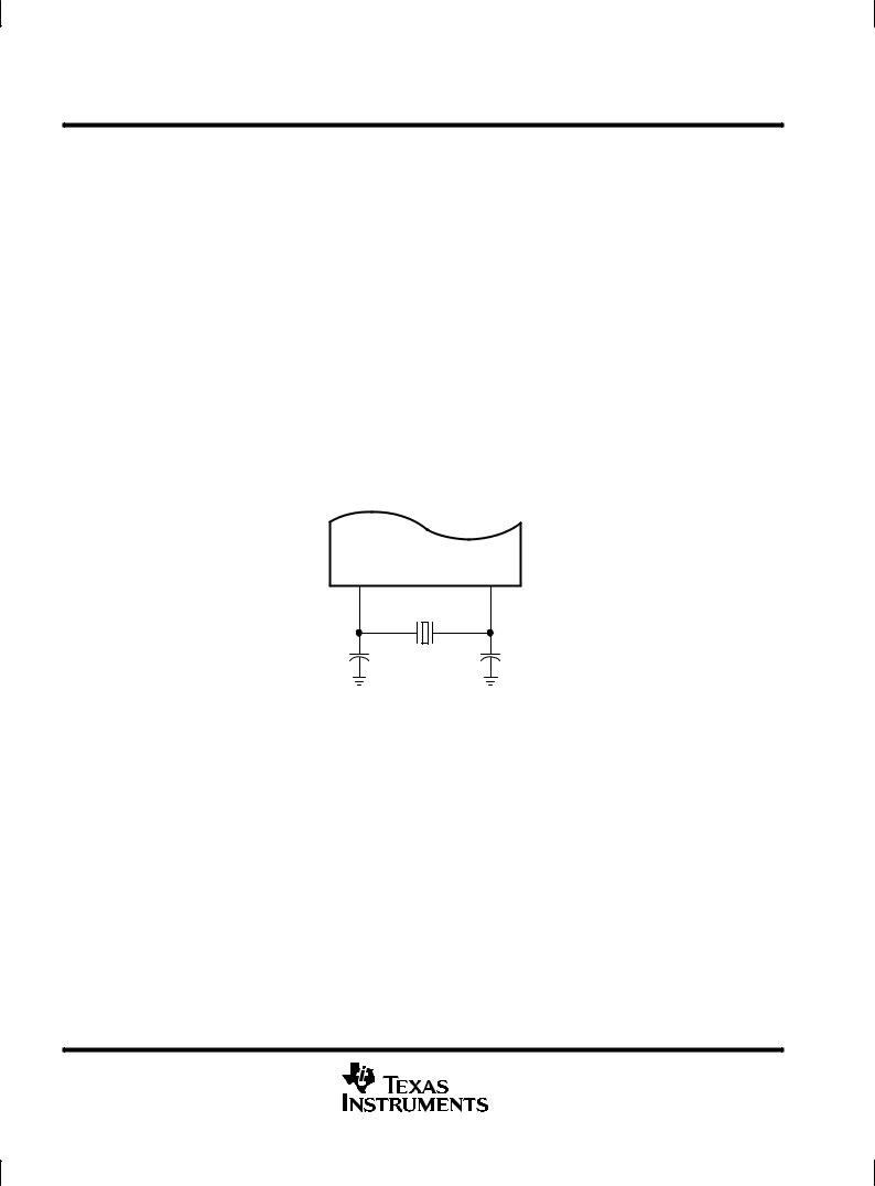
TMS320VC549
FIXED POINT DIGITAL SIGNAL PROCESSOR
SPRS078F ± SEPTEMBER 1998 ± REVISED MAY 2000
internal oscillator with external crystal
The internal oscillator is enabled by selecting the appropriate clock mode at reset (this is device dependent ± see PLL section) and connecting a crystal or ceramic resonator across X1 and X2/CLKIN. The CPU clock frequency is one-half the crystal's oscillation frequency following reset. After reset, the clock mode of the devices with the software PLL can also be changed to divide-by-four.
The crystal should be in fundamental mode operation and parallel resonant with an effective series resistance of 30ohms and power dissipation of 1 mW. The connection of the required circuit, consisting of the crystal and two load capacitors, is shown in Figure 2. The load capacitors, C1 and C2, should be chosen such that the equation below is satisfied. CL in the equation is the load specified for the crystal.
|
|
CL + |
C1C2 |
|
|
|
|
|
|
|
|
|
(C1 )C2) |
|
|
|
|
||||
|
|
|
|
|
|
|
||||
recommended operating conditions (see Figure 2) |
|
|
|
|
|
|
|
|
||
|
|
|
|
|
|
|
|
|
|
|
|
|
'549-80 |
|
|
|
|
'549-100 |
|
'549-120 |
UNIT |
|
|
|
|
|
|
|
|
|
|
|
|
|
MIN NOM |
MAX |
|
MIN |
NOM MAX |
MIN |
NOM MAX |
||
|
|
|
|
|||||||
|
|
|
|
|
|
|
|
|
|
|
fx |
Input clock frequency |
10² |
20³ |
|
10² |
20³ |
10² |
20³ |
MHz |
|
²This device utilizes a fully static design and therefore can operate with tc(CI) approaching ∞ . The device is characterized at frequencies approaching 0 Hz.
³ It is recommended that the PLL clocking option be used for maximum frequency operation.
X1 |
X2/CLKIN |
|
Crystal |
C1 |
C2 |
Figure 2. Internal Divide-by-Two Clock Option With External Crystal
14 |
POST OFFICE BOX 1443 •HOUSTON, TEXAS 77251±1443 |

TMS320VC549
FIXED POINT DIGITAL SIGNAL PROCESSOR
SPRS078F ± SEPTEMBER 1998 ± REVISED MAY 2000
divide-by-two/divide-by-four clock option ± PLL disabled
The frequency of the reference clock provided at the X2/CLKIN pin can be divided by a factor of two or four to generate the internal machine cycle.
When an external clock source is used, the frequency injected must conform to specifications listed in the timing requirements table.
switching characteristics over recommended operating conditions for divide-by-two/
divide-by-four clock option ± PLL disabled [H = 0.5tc(CO)] (see Figure 2 and Figure 3, and the recommended operating conditions table)
|
PARAMETER |
|
'549-80 |
|
|
'549-100 |
|
|
'549-120 |
|
UNIT |
|
|
|
|
|
|
|
|
|
|
|
|||
|
MIN |
TYP |
MAX |
MIN |
TYP |
MAX |
MIN |
TYP |
MAX |
|||
|
|
|
||||||||||
|
|
|
|
|
|
|
|
|
|
|
|
|
tc(CO) |
Cycle time, CLKOUT |
12.5³ |
2tc(CI) |
² |
10³ |
2tc(CI) |
² |
8.33³ |
2tc(CI) |
² |
ns |
|
td(CIH-CO) |
Delay time, X2/CLKIN high to |
3 |
6 |
10 |
3 |
6 |
10 |
3 |
6 |
10 |
ns |
|
CLKOUT high/low |
||||||||||||
|
|
|
|
|
|
|
|
|
|
|
||
|
|
|
|
|
|
|
|
|
|
|
|
|
tf(CO) |
Fall time, CLKOUT² |
|
2 |
|
|
2 |
|
|
2 |
|
ns |
|
tr(CO) |
Rise time, CLKOUT² |
|
2 |
|
|
2 |
|
|
2 |
|
ns |
|
tw(COL) |
Pulse duration, CLKOUT low² |
H±3 |
H±1 |
H |
H±2 |
H±1 |
H |
H±2 |
H±1 |
H |
ns |
|
tw(COH) |
Pulse duration, CLKOUT high² |
H±3 |
H±1 |
H |
H±2 |
H±1 |
H |
H±2 |
H±1 |
H |
ns |
²This device utilizes a fully static design and therefore can operate with tc(CI) approaching ∞ . The device is characterized at frequencies approaching 0 Hz.
³ It is recommended that the PLL clocking option be used for maximum frequency operation.
POST OFFICE BOX 1443 •HOUSTON, TEXAS 77251±1443 |
15 |
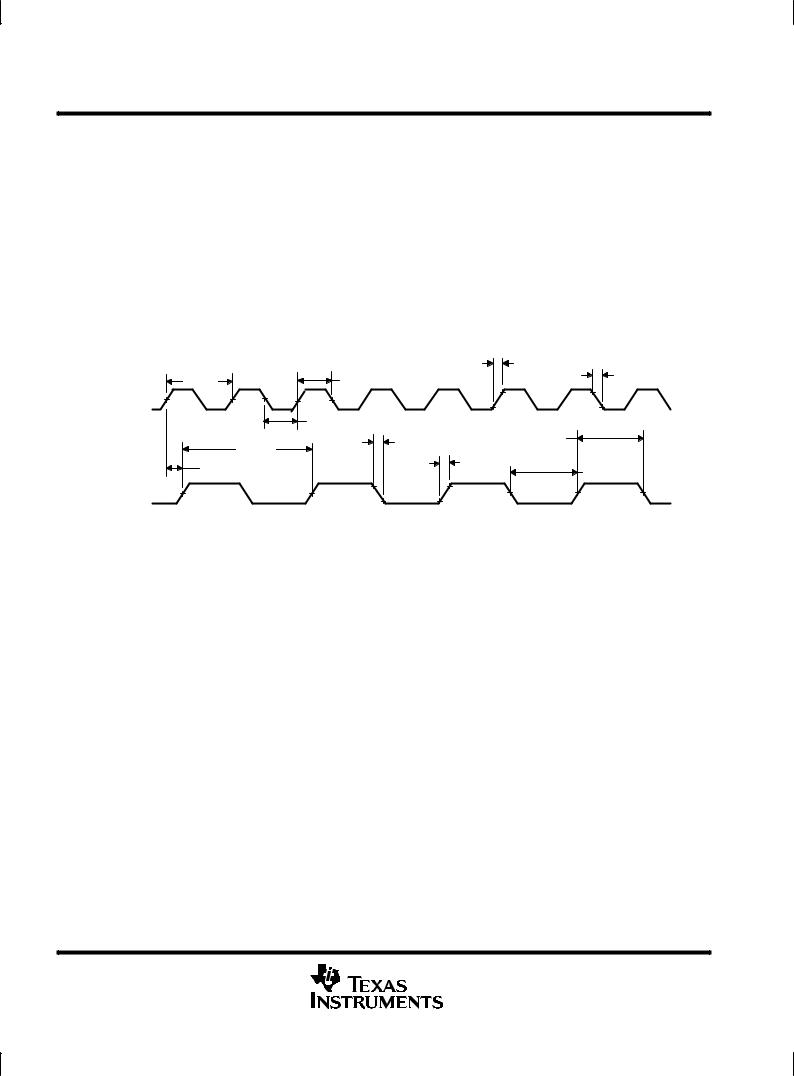
TMS320VC549
FIXED POINT DIGITAL SIGNAL PROCESSOR
SPRS078F ± SEPTEMBER 1998 ± REVISED MAY 2000
divide-by-two/divide-by-four clock option ± PLL disabled (continued)
timing requirements for divide-by-two/divide-by-four clock option ± PLL disabled (see Figure 3)
|
|
'549-80 |
'549-100 |
'549-120 |
UNIT |
|||
|
|
|
|
|
|
|
|
|
|
|
MIN |
MAX |
MIN |
MAX |
MIN |
MAX |
|
|
|
|
||||||
|
|
|
|
|
|
|
|
|
tc(CI) |
Cycle time, X2/CLKIN |
20³ |
² |
20³ |
² |
20³ |
² |
ns |
tf(CI) |
Fall time, X2/CLKIN |
|
8 |
|
8 |
|
8 |
ns |
tr(CI) |
Rise time, X2/CLKIN |
|
8 |
|
8 |
|
8 |
ns |
tw(CIL) |
Pulse duration, X2/CLKIN low |
5 |
² |
5 |
² |
5 |
² |
ns |
tw(CIH) |
Pulse duration, X2/CLKIN high |
5 |
² |
5 |
² |
5 |
² |
ns |
²This device utilizes a fully static design and therefore can operate with tc(CI) approaching ∞ . The device is characterized at frequencies approaching 0 Hz.
³ It is recommended that the PLL clocking option be used for maximum frequency operation.
|
|
|
tr(CI) |
tc(CI) |
tw(CIH) |
|
tf(CI) |
X2/CLKIN |
|
|
|
|
tw(CIL) |
|
|
tc(CO) |
tf(CO) |
|
tw(COH) |
|
tr(CO) |
|
|
td(CIH-CO) |
|
tw(COL) |
|
|
|
||
CLKOUT |
|
|
|
Figure 3. External Divide-by-Two Clock Timing
16 |
POST OFFICE BOX 1443 •HOUSTON, TEXAS 77251±1443 |

TMS320VC549
FIXED POINT DIGITAL SIGNAL PROCESSOR
SPRS078F ± SEPTEMBER 1998 ± REVISED MAY 2000
multiply-by-N clock option ± PLL enabled
The frequency of the reference clock provided at the X2/CLKIN pin can be multiplied by a factor of N to generate the internal machine cycle.
When an external clock source is used, the frequency injected must conform to specifications listed in the timing requirements table.
switching characteristics over recommended operating conditions for multiply-by-N clock option
± PLL enabled [H = 0.5tc(CO)] (see Figure 2 and Figure 4, and the recommended operating conditions table)
|
PARAMETER |
|
'549-80 |
|
|
'549-100 |
|
|
'549-120 |
|
UNIT |
|
|
|
|
|
|
|
|
|
|
|
|||
|
MIN |
TYP |
MAX |
MIN |
TYP |
MAX |
MIN |
TYP |
MAX |
|||
|
|
|
||||||||||
|
|
|
|
|
|
|
|
|
|
|
|
|
tc(CO) |
Cycle time, CLKOUT |
12.5 |
tc(CI)/N |
|
10 |
tc(CI)/N |
|
8.33 |
tc(CI)/N |
|
ns |
|
td(CIH-CO) |
Delay time, X2/CLKIN high/low to |
3 |
6 |
10 |
3 |
6 |
10 |
3 |
6 |
10 |
ns |
|
CLKOUT high/low |
||||||||||||
|
|
|
|
|
|
|
|
|
|
|
||
|
|
|
|
|
|
|
|
|
|
|
|
|
tf(CO) |
Fall time, CLKOUT |
|
2 |
|
|
2 |
|
|
2 |
|
ns |
|
tr(CO) |
Rise time, CLKOUT |
|
2 |
|
|
2 |
|
|
2 |
|
ns |
|
tw(COL) |
Pulse duration, CLKOUT low |
H±3 |
H±1 |
H |
H±2 |
H±1 |
H |
H±2 |
H±1 |
H |
ns |
|
tw(COH) |
Pulse duration, CLKOUT high |
H±3 |
H±1 |
H |
H±2 |
H±1 |
H |
H±2 |
H±1 |
H |
ns |
|
tp |
Transitory phase, PLL lock-up time |
|
|
29 |
|
|
35 |
|
|
45 |
s |
POST OFFICE BOX 1443 •HOUSTON, TEXAS 77251±1443 |
17 |
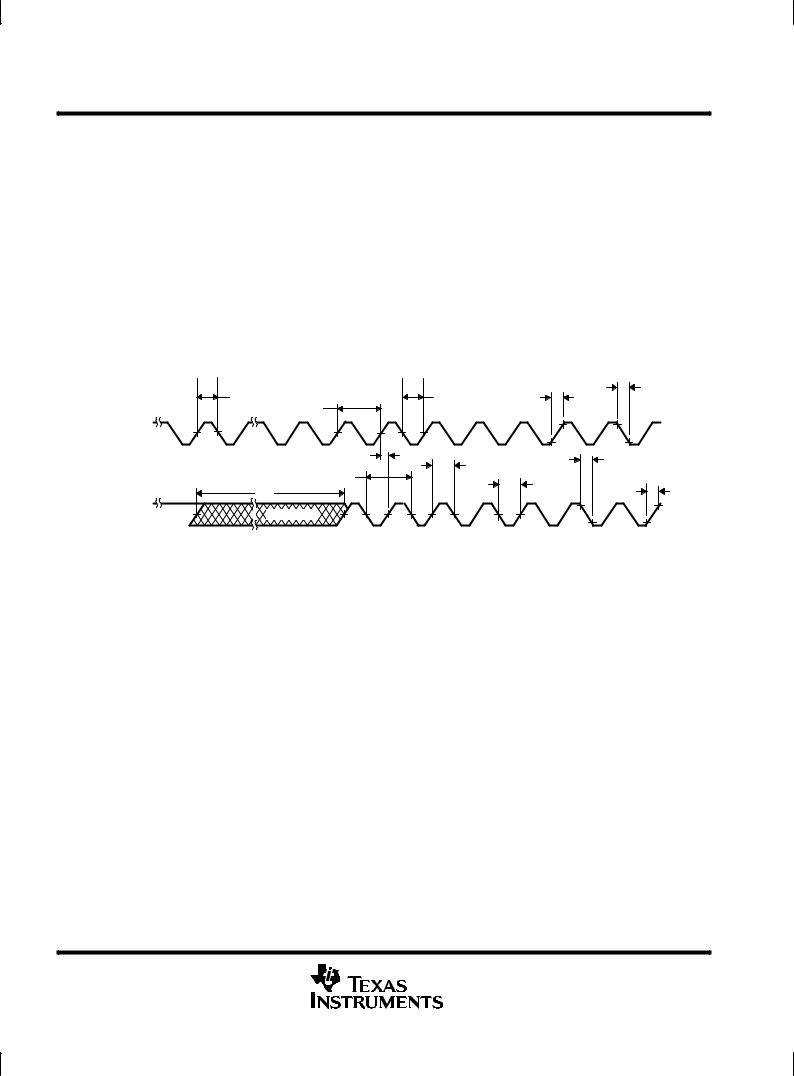
TMS320VC549
FIXED POINT DIGITAL SIGNAL PROCESSOR
SPRS078F ± SEPTEMBER 1998 ± REVISED MAY 2000
multiply-by-N clock option ± PLL enabled (continued)
timing requirements for multiply-by-N clock option ± PLL enabled (see Figure 4)
|
|
|
'549-80 |
'549-100 |
|
||
|
|
|
'549-120 |
UNIT |
|||
|
|
|
|
|
|||
|
|
|
|
|
|
|
|
|
|
|
MIN |
MAX |
MIN |
MAX |
|
|
|
|
|
|
|
|
|
|
|
Integer PLL multiplier N (N = 1±15) |
20² |
200 |
20² |
200 |
|
tc(CI) |
Cycle time, X2/CLKIN |
PLL multiplier N = x.5 |
20² |
100 |
20² |
100 |
ns |
|
|
PLL multiplier N = x.25, x.75 |
20² |
50 |
20² |
50 |
|
tf(CI) |
Fall time, X2/CLKIN |
|
|
8 |
|
8 |
ns |
tr(CI) |
Rise time, X2/CLKIN |
|
|
8 |
|
8 |
ns |
tw(CIL) |
Pulse duration, X2/CLKIN low |
|
5 |
|
5 |
|
ns |
tw(CIH) |
Pulse duration, X2/CLKIN high |
|
5 |
|
5 |
|
ns |
² Note that for all values of t |
c(CI) |
, the minimum t |
c(CO) |
period must not be exceeded. |
|
|
|
|
|
|
|
||
|
|
tw(CIH) |
|
tw(CIL) |
tr(CI) |
tf(CI) |
|
|
|
tc(CI) |
|
|
|
X2/CLKIN |
|
|
|
|
|
|
|
|
|
|
td(CIH-CO) |
tf(CO) |
|
|
|
|
|
tw(COH) |
|
|
|
|
|
|
tc(CO) |
tw(COL) |
tr(CO) |
|
|
tp |
|
|
||
|
|
|
|
|
||
CLKOUT |
|
Unstable |
|
|
||
Figure 4. External Multiply-by-One Clock Timing
18 |
POST OFFICE BOX 1443 •HOUSTON, TEXAS 77251±1443 |
 Loading...