


 Loading...
Texas Instruments TPS3831A09DQNR, TPS3831E16DQNR, TPS3831G12DQNR, TPS3831G18DQNR, TPS3831G33DQNR Schematic [ru]
...PRODUCT |
SAMPLE & |
TECHNICAL |
TOOLS & |
SUPPORT & |
FOLDER |
BUY |
DOCUMENTS |
SOFTWARE |
COMMUNITY |
TPS3831, TPS3839
SBVS193D –JUNE 2012–REVISED JULY 2015
TPS383x 150-nA, Ultralow Power, Supply Voltage Monitor
1 Features
•Ultralow Supply Current: 150 nA (Typical)
•Operating Supply Voltage: 0.9 V to 6.5 V
•Valid Reset for VDD > 0.6 V
•Push-Pull RESET Output
•Factory-Trimmed Reset Threshold Voltages
•Temperature Range: –40°C to 85°C
•Packages: 1-mm × 1-mm X2SON or 3-Pin SOT23
2 Applications
•Portable and Battery-Powered Equipment
•Metering
•Industrial Equipment
•Cell Phones
•Glucose Monitors
•Tablets
•Wearables
3 Description
The TPS3831 and TPS3839 devices (both referred to as TPS383x) are ultralow current (150 nA, typical), voltage supervisory circuits that monitor a single voltage. Both devices initiate an active-low reset signal whenever the VDD supply voltage drops below the factory-trimmed reset threshold voltage. The reset output remains low for 200 ms (typical) after the VDD voltage rises above the threshold voltage and hysteresis. These devices are designed to ignore fast transients on the VDD pin. The TPS3831 device includes a manual reset input that forces RESET low
when MR is low.
The ultralow current consumption of 150 nA makes these voltage supervisors ideal for use in low-power and portable applications. The TPS383x devices are specified to have the correct output logic state for supply voltages down to 0.6 V.
The TPS383x devices feature precision factorytrimmed threshold voltages and extremely low-power operation. The TPS3831 device is available in a 4- pin, 1-mm × 1-mm (DQN) X2SON package. The TPS3839 device is available in a 3-pin SOT23 (DBZ) package or a 4-pin, 1-mm × 1-mm (DQN) X2SON package.
Device Information(1)
PART NUMBER |
PACKAGE |
PACKAGE SIZE |
|
(NOM) |
|||
|
|
||
TPS3831 |
X2SON (4) |
1.00 mm x 1.00 mm |
|
TPS3839 |
SOT-23 (3) |
2.92 mm x 2.37 mm |
|
X2SON (4) |
1.00 mm x 1.00 mm |
||
|
(1)For all available packages, see the orderable addendum at the end of the data sheet.
Typical Application Circuit |
Supply Current vs Temperature |
|
3.3 V |
|
|
200 |
VDD = 1.2 V |
|
|
|
|
|
|
|
|
190 |
|
|
|
|
|
|
|
|
|
VDD = 3.3 V |
|
|
|
|
|
C1 |
|
|
|
|
|
|
|
|
|
|
|
|
180 |
VDD = 5.0 V |
|
|
|
|
|
0.1 mF |
|
|
(nA) |
170 |
VDD = 6.5 V |
|
|
|
|
|
|
|
|
|
|
|
|
||
|
|
|
|
|
|
|
|
|
|
|
VDD |
|
Current |
160 |
|
|
|
|
|
TPS383xK33 |
MICROPROCESSOR |
150 |
|
|
|
|
|
||
|
|
|
|
|
|
||||
Supply |
|
|
|
|
|
|
|||
|
|
|
140 |
|
|
|
|
|
|
|
|
|
|
|
|
|
|
|
|
MR |
RESET |
RST |
|
130 |
|
|
|
|
|
|
|
|
|
|
|
|
|
|
|
TPS3831 |
GND |
|
|
120 |
|
|
|
|
|
Only |
|
|
|
110 |
|
|
|
|
|
|
|
|
|
|
|
|
|
|
|
|
|
|
|
100 |
−15 |
10 |
35 |
60 |
85 |
|
|
|
|
−40 |
|||||
|
|
|
|
|
|
Temperature (°C) |
|
G001 |
|
|
|
|
|
|
|
|
|
|
|
An IMPORTANT NOTICE at the end of this data sheet addresses availability, warranty, changes, use in safety-critical applications, intellectual property matters and other important disclaimers. PRODUCTION DATA.

TPS3831, TPS3839
SBVS193D –JUNE 2012 –REVISED JULY 2015 www.ti.com
Table of Contents
1 |
Features .................................................................. |
1 |
|
8.4 |
Device Functional Modes........................................ |
12 |
|
2 |
Applications ........................................................... |
1 |
9 |
Applications and Implementation ...................... |
13 |
||
3 |
Description ............................................................. |
1 |
|
9.1 |
Application Information............................................ |
13 |
|
4 |
Revision History..................................................... |
2 |
|
9.2 |
Typical Application .................................................. |
13 |
|
5 |
Device Options....................................................... |
4 |
10 |
Power Supply Recommendations ..................... |
15 |
||
6 |
Pin Configuration and Functions ......................... |
5 |
11 |
Layout................................................................... |
15 |
||
7 |
Specifications |
6 |
|
11.1 |
Layout Guidelines ................................................. |
15 |
|
|
11.2 |
Layout Example |
15 |
||||
|
7.1 |
Absolute Maximum Ratings |
6 |
|
|||
|
12 Device and Documentation Support |
16 |
|||||
|
7.2 |
ESD Ratings.............................................................. |
6 |
||||
|
7.3 |
Recommended Operating Conditions |
6 |
|
12.1 |
Device Support...................................................... |
16 |
|
|
12.2 |
Documentation Support |
16 |
|||
|
7.4 |
Thermal Information |
6 |
|
|||
|
|
12.3 |
Related Links |
16 |
|||
|
7.5 |
Electrical Characteristics |
7 |
|
|||
|
|
12.4 |
Community Resources |
16 |
|||
|
7.6 |
Timing Requirements |
8 |
|
|||
|
|
12.5 |
Trademarks |
16 |
|||
|
7.7 |
Typical Characteristics |
9 |
|
|||
|
|
12.6 |
Electrostatic Discharge Caution |
16 |
|||
8 |
Detailed Description |
11 |
|
||||
|
12.7 |
Glossary |
17 |
||||
|
8.1 |
Overview |
11 |
|
|||
|
13 Mechanical, Packaging, and Orderable |
|
|||||
|
8.2 |
Functional Block Diagram ....................................... |
11 |
17 |
|||
|
8.3 |
Feature Description |
11 |
|
Information ........................................................... |
||
|
|
|
|
|
|||
|
|
|
|
|
|
|
|
4 |
Revision History |
|
NOTE: Page numbers for previous revisions may differ from page numbers in the current version. |
|
|
Changes from Revision C (February 2015) to Revision D |
Page |
|
|
|
|
• |
Changed µA to nA in document title....................................................................................................................................... |
1 |
• |
Added TPS3839G25 to document ......................................................................................................................................... |
1 |
• |
Changed Applications section: moved Metering bullet to second in list, changed Tablets bullet, added Wearables bullet .. 1 |
|
• |
Changed first paragraph of Description section .................................................................................................................... |
1 |
• |
Changed Device Information table: changed Package Size column heading and value of SOT-23 row ............................. |
1 |
• |
Added TPS3839G25 row to Device Options table ................................................................................................................ |
4 |
• |
Changed Thermal Information table ...................................................................................................................................... |
6 |
•Changed VIT– and Vhys parameters in Electrical Characteristics table: changed test conditions, added TPS3839G25 rows 7
Changes from Revision B (April 2013) to Revision C |
Page |
•Added ESD Ratings table, Feature Description section, Device Functional Modes, Application and Implementation section, Power Supply Recommendations section, Layout section, Device and Documentation Support section, and
Mechanical, Packaging, and Orderable Information section ................................................................................................. |
1 |
• Changed title of data sheet ................................................................................................................................................... |
1 |
• Changed Operating Supply Voltage bullet from 0.6 V to 0.9 V.............................................................................................. |
1 |
• Changed last sentence of Description section ...................................................................................................................... |
1 |
• Changed front page figure ..................................................................................................................................................... |
1 |
• Added MR parameter to Absolute Maximum Ratings ........................................................................................................... |
6 |
• Changed condition statement for Electrical Characteristics .................................................................................................. |
7 |
• Changed V(VO) parameter symbol to VPOR ............................................................................................................................. |
7 |
• Changed Figure 1................................................................................................................................................................... |
8 |
• Changed Functional Block Diagram; added hysteresis symbol to op amp .......................................................................... |
11 |
• Deleted Typical Application Circuit figure ............................................................................................................................. |
13 |
2 |
Submit Documentation Feedback |
Copyright © 2012–2015, Texas Instruments Incorporated |

|
TPS3831, TPS3839 |
www.ti.com |
SBVS193D – JUNE 2012 – REVISED JULY 2015 |
Changes from Revision A (September 2012) to Revision B |
Page |
• Changed VDD test conditions for high-level output voltage parameter |
................................................................................... 7 |
Changes from Original (June 2012) to Revision A |
Page |
• Changed data sheet status from product preview to production data.................................................................................... |
1 |
Copyright © 2012–2015, Texas Instruments Incorporated |
Submit Documentation Feedback |
3 |

TPS3831, TPS3839
SBVS193D –JUNE 2012 –REVISED JULY 2015 |
|
|
www.ti.com |
|
5 Device Options |
|
|
|
|
|
|
|
|
|
PRODUCT |
|
THRESHOLD |
PACKAGE-LEAD |
PACKAGE |
|
VOLTAGE (V) |
DESIGNATOR(1) |
||
TPS3831A09 |
|
0.9 |
X2SON-4 |
DQN |
TPS3831G12 |
|
1.1 |
X2SON-4 |
DQN |
TPS3831E16 |
|
1.52 |
X2SON-4 |
DQN |
TPS3831G18 |
|
1.67 |
X2SON-4 |
DQN |
TPS3831L30 |
|
2.63 |
X2SON-4 |
DQN |
TPS3831K33 |
|
2.93 |
X2SON-4 |
DQN |
TPS3831G33 |
|
3.08 |
X2SON-4 |
DQN |
TPS3831K50 |
|
4.38 |
X2SON-4 |
DQN |
TPS3839A09 |
|
0.9 |
SOT23-3 |
DBZ |
|
X2SON-4 |
DQN |
||
|
|
|
||
TPS3839G12 |
|
1.1 |
SOT23-3 |
DBZ |
|
X2SON-4 |
DQN |
||
|
|
|
||
TPS3839E16 |
|
1.52 |
SOT23-3 |
DBZ |
|
X2SON-4 |
DQN |
||
|
|
|
||
TPS3839G18 |
|
1.67 |
SOT23-3 |
DBZ |
|
X2SON-4 |
DQN |
||
|
|
|
||
TPS3839G25 |
|
2.325 |
SOT23-3 |
DBZ |
TPS3839L30 |
|
2.63 |
SOT23-3 |
DBZ |
|
X2SON-4 |
DQN |
||
|
|
|
||
TPS3839K33 |
|
2.93 |
SOT23-3 |
DBZ |
|
X2SON-4 |
DQN |
||
|
|
|
||
TPS3839G33 |
|
3.08 |
SOT23-3 |
DBZ |
|
X2SON-4 |
DQN |
||
|
|
|
||
TPS3839K50 |
|
4.38 |
SOT23-3 |
DBZ |
|
X2SON-4 |
DQN |
||
|
|
|
||
(1)For the most current package and ordering information see the Package Option Addendum at the end of this document, or visit the device product folder at www.ti.com.
4 |
Submit Documentation Feedback |
Copyright © 2012–2015, Texas Instruments Incorporated |

TPS3831, TPS3839
www.ti.com |
SBVS193D –JUNE 2012–REVISED JULY 2015 |
6 Pin Configuration and Functions
TPS3831 DQN Package
1-mm × 1-mm X2SON
Top View
RESET |
1 |
4 |
VDD |
|
|
THERMAL |
|
|
|
PAD |
|
MR |
2 |
3 |
GND |
TPS3839 DQN Package
1-mm × 1-mm X2SON
Top View
RESET |
1 |
4 |
VDD |
|
|
THERMAL |
|
|
|
PAD |
|
NC |
2 |
3 |
GND |
TPS3839 DBZ Package
SOT23-3
Top View
|
|
|
|
|
|
|
|
GND |
|
1 |
|
|
|
|
|
|
|
|
|
|
|
||
|
|
|
|
|
|
|
|
|
|
|
|
|
|
|
|
|
|
|
|
||||
|
|
|
|
|
|
|
|
|
|
|
|
3 |
|
VDD |
|||||||||
|
|
|
|
|
|
|
|
|
|
|
|
|
|||||||||||
|
|
|
|
|
|
|
|
|
|
|
|
2 |
|
|
|
|
|
|
|
|
|
|
|
|
|
|
|
|
|
|
|
RESET |
|
|
|
|
|
|
|
|
|
|
|
|
|||
|
|
|
|
|
|
|
|
|
|
|
|
|
|
|
|
|
|
|
|
|
|
|
|
|
|
|
|
|
|
|
|
|
|
|
Pin Functions |
|
|
|
|
|
|
|
|
|
|||
|
|
|
|
PIN |
|
|
|
|
|
|
|
|
|
|
|
|
|
|
|
|
|
|
|
|
|
NAME |
|
|
NO. |
|
|
|
|
I/O |
|
|
|
|
DESCRIPTION |
||||||||
|
|
TPS3839 |
|
TPS3839 |
TPS3831 |
|
|
|
|
|
|
||||||||||||
|
|
|
|
|
|
|
|
|
|
|
|
|
|
|
|
|
|
||||||
|
|
|
|
(SOT23-3) |
|
(X2SON) |
(X2SON) |
|
|
|
|
|
|
|
|
|
|
|
|
|
|
|
|
|
GND |
1 |
|
3 |
3 |
|
|
|
— |
|
Ground |
|
|
|
|
|
|
|
|
|
|||
|
|
|
|
|
|
|
|
|
|
|
|
|
Manual reset. Pull this pin to a logic low to assert the |
|
output. |
||||||||
|
|
|
|
|
|
|
|
|
|
|
|
|
RESET |
||||||||||
|
MR |
|
N/A |
|
N/A |
2 |
|
|
|
I |
|
After the MR pin is deasserted, the |
RESET |
output deasserts after the |
|||||||||
|
|
|
|
|
|
|
|
|
|
|
|
|
reset delay (td) elapses. |
||||||||||
|
NC |
N/A |
|
2 |
N/A |
|
|
— |
|
No internal connection. |
|||||||||||||
|
|
|
|
|
|
|
|
|
|
|
|
|
Active-low reset output. |
|
has a push-pull output drive and is |
||||||||
|
|
|
|
|
|
|
|
|
|
|
|
|
RESET |
||||||||||
|
|
|
|
2 |
|
1 |
1 |
|
|
|
O |
|
capable of directly driving input pins. |
RESET |
is low as long as VDD |
||||||||
|
RESET |
|
|
|
|
|
|||||||||||||||||
|
|
|
|
|
|
|
|
|
|
|
|
|
remains below the factory threshold voltage, and until the delay time |
||||||||||
|
|
|
|
|
|
|
|
|
|
|
|
|
(td) elapses after VDD rises above the threshold voltage. |
||||||||||
|
Thermal pad |
N/A |
|
Available |
Available |
|
|
— |
|
Connect to ground or to a floating copper plane for mechanical |
|||||||||||||
|
|
|
|
|
stability. |
|
|
|
|
|
|
|
|
|
|||||||||
|
|
|
|
|
|
|
|
|
|
|
|
|
|
|
|
|
|
|
|
|
|
||
|
VDD |
3 |
|
4 |
4 |
|
|
|
I |
|
Supply voltage |
||||||||||||
Copyright © 2012–2015, Texas Instruments Incorporated |
Submit Documentation Feedback |
5 |

TPS3831, TPS3839
SBVS193D –JUNE 2012 –REVISED JULY 2015 |
www.ti.com |
7 Specifications
7.1 Absolute Maximum Ratings
over operating free-air temperature range, unless otherwise noted(1)
|
|
|
|
|
|
|
MIN |
MAX |
UNIT |
Voltage |
|
VDD, |
RESET |
|
–0.3 |
7 |
V |
||
|
|
|
|
|
|
|
|
|
|
|
MR |
–0.3 |
VDD + 0.3 |
V |
|||||
|
|
||||||||
Current |
|
|
|
|
pin |
–10 |
10 |
mA |
|
|
RESET |
||||||||
Temperature(2) |
|
Operating ambient, TA |
–40 |
85 |
°C |
||||
|
Storage, Tstg |
–65 |
150 |
||||||
|
|
|
|||||||
(1)Stresses beyond those listed under Absolute Maximum Ratings may cause permanent damage to the device. These are stress ratings only, and functional operation of the device at these or any other conditions beyond those indicated under Recommended Operating Conditions is not implied. Exposure to absolute-maximum-rated conditions for extended periods may affect device reliability.
(2)As a result of the low dissipated power in this device, the junction temperature is assumed to be equal to the ambient temperature.
7.2 |
ESD Ratings |
|
|
|
||
|
|
|
|
VALUE |
UNIT |
|
V(ESD) |
Electrostatic discharge |
Human body model (HBM), per ANSI/ESDA/JEDEC JS-001(1) |
|
±2000 |
V |
|
Charged device model (CDM), per JEDEC specification JESD22-C101 |
(2) |
±500 |
||||
|
|
|
||||
(1)JEDEC document JEP155 states that 500-V HBM allows safe manufacturing with a standard ESD control process.
(2)JEDEC document JEP157 states that 250-V CDM allows safe manufacturing with a standard ESD control process.
7.3 Recommended Operating Conditions
over operating free-air temperature range (unless otherwise noted)
|
|
|
|
|
|
|
|
MIN |
NOM |
MAX |
UNIT |
VDD |
Input supply voltage |
0.9 |
|
6.5 |
V |
||||||
V |
|
|
Manual reset pin voltage |
0 |
|
VDD |
V |
||||
MR |
|
||||||||||
V |
|
|
|
|
pin voltage |
0 |
|
6.5 |
V |
||
|
|
|
|
RESET |
|
||||||
RESET |
|
||||||||||
I |
|
|
|
|
|
|
pin current |
0 |
|
8 |
mA |
|
|
|
|
|
RESET |
|
|||||
RESET |
|
||||||||||
7.4 Thermal Information
|
|
TPS3839 |
TPS3831, |
|
|
|
TPS3839 |
|
|
|
THERMAL METRIC(1) |
|
UNIT |
|
|
DBZ (SOT23-3) |
DQN (X2SON) |
||
|
|
|
||
|
|
3 PINS |
4 PINS |
|
RθJA |
Junction-to-ambient thermal resistance |
346.6 |
216.1 |
°C/W |
RθJC(top) |
Junction-to-case (top) thermal resistance |
124.4 |
161.7 |
°C/W |
RθJB |
Junction-to-board thermal resistance |
78.9 |
162.1 |
°C/W |
ψJT |
Junction-to-top characterization parameter |
11.5 |
5.1 |
°C/W |
ψJB |
Junction-to-board characterization parameter |
77.3 |
161.7 |
°C/W |
RθJC(bot) |
Junction-to-case (bottom) thermal resistance |
N/A |
123.0 |
°C/W |
(1)For more information about traditional and new thermal metrics, see the Semiconductor and IC Package Thermal Metrics application report, SPRA953.
6 |
Submit Documentation Feedback |
Copyright © 2012–2015, Texas Instruments Incorporated |

TPS3831, TPS3839
www.ti.com |
SBVS193D –JUNE 2012–REVISED JULY 2015 |
7.5 Electrical Characteristics
At TA = –40°C to 85°C, 0.9 V < VDD < 6.5 V, and C1 = 0.1 µF, unless otherwise noted. Typical values are at 25°C.
|
|
|
PARAMETER |
TEST CONDITIONS |
MIN |
TYP |
MAX |
UNIT |
||||||||
VDD |
Input supply voltage |
|
0.9 |
|
6.5 |
V |
||||||||||
V(POR) |
Minimum VDD voltage for valid output |
IOL = 1 µA |
|
|
0.6 |
V |
||||||||||
IDD |
Supply current (into VDD pin) |
Output not connected |
|
150 |
500 |
nA |
||||||||||
|
|
|
|
|
|
|
|
|
|
|
|
VDD = 0.9 V to 1.2 V, IOL = 120 µA |
|
|
0.4 |
|
VOL |
Low-level output voltage |
|
pin) |
VDD = 1.2 V to 2.8 V, IOL = 0.5 mA |
|
|
0.4 |
V |
||||||||
(RESET |
|
|
||||||||||||||
|
|
|
|
|
|
|
|
|
|
|
|
VDD = 2.8 V to 6.5 V, IOL = 2 mA |
|
|
0.4 |
|
|
|
|
|
|
|
|
|
|
|
|
|
VDD = 0.9 V to 1.2 V, IOH = –50 µA |
VDD – 0.4 |
|
|
|
VOH |
High-level output voltage |
|
|
pin) |
VDD = 1.2 V to 3.3 V, IOH = –0.5 mA |
VDD – 0.4 |
|
|
V |
|||||||
(RESET |
|
|
||||||||||||||
|
|
|
|
|
|
|
|
|
|
|
|
VDD = 3.3 V to 6.5 V, IOH = –2 mA |
VDD – 0.4 |
|
|
|
VIL |
Low-level input voltage |
|
|
|
pin) |
|
0.3VDD |
|
|
V |
||||||
(MR |
|
|
|
|||||||||||||
VIH |
High-level input voltage |
|
|
|
|
pin) |
|
|
|
0.7VDD |
V |
|||||
(MR |
|
|
|
|||||||||||||
R |
|
|
MR pin pullup resistance |
|
10 |
20 |
30 |
kΩ |
||||||||
MR |
|
|||||||||||||||
|
|
|
Negative-going input threshold accuracy |
TA = 25°C |
|
±1% |
|
|
||||||||
|
|
|
|
|
|
|
|
|
|
|
|
TPS383xA09 |
0.874 |
0.9 |
0.914 |
|
|
|
|
|
|
|
|
|
|
|
|
|
TPS383xG12 |
1.073 |
1.1 |
1.117 |
|
|
|
|
|
|
|
|
|
|
|
|
|
TPS383xE16 |
1.482 |
1.52 |
1.543 |
|
|
|
|
|
|
|
|
|
|
|
|
|
TPS383xG18 |
1.628 |
1.67 |
1.695 |
|
VIT– |
Negative-going threshold voltage |
TPS3839G25 |
2.267 |
2.325 |
2.360 |
V |
||||||||||
|
|
|
|
|
|
|
|
|
|
|
|
TPS383xL30 |
2.564 |
2.63 |
2.669 |
|
|
|
|
|
|
|
|
|
|
|
|
|
TPS383xK33 |
2.857 |
2.93 |
2.974 |
|
|
|
|
|
|
|
|
|
|
|
|
|
TPS383xG33 |
3.003 |
3.08 |
3.126 |
|
|
|
|
|
|
|
|
|
|
|
|
|
TPS383xK50 |
4.271 |
4.38 |
4.446 |
|
|
|
|
|
|
|
|
|
|
|
|
|
TPS383xA09 |
|
54 |
|
|
|
|
|
|
|
|
|
|
|
|
|
|
TPS383xG12 |
|
11 |
|
|
|
|
|
|
|
|
|
|
|
|
|
|
TPS383xE16 |
|
15 |
|
|
|
|
|
|
|
|
|
|
|
|
|
|
TPS383xG18 |
|
17 |
|
|
Vhys |
Hysteresis voltage |
TPS383xL30 |
|
26 |
|
mV |
||||||||||
|
|
|
|
|
|
|
|
|
|
|
|
TPS3839G25 |
|
23 |
|
|
|
|
|
|
|
|
|
|
|
|
|
|
TPS383xK33 |
|
29 |
|
|
|
|
|
|
|
|
|
|
|
|
|
|
TPS383xG33 |
|
31 |
|
|
|
|
|
|
|
|
|
|
|
|
|
|
TPS383xK50 |
|
44 |
|
|
Copyright © 2012–2015, Texas Instruments Incorporated |
Submit Documentation Feedback |
7 |
TPS3831, TPS3839
SBVS193D –JUNE 2012 –REVISED JULY 2015 |
www.ti.com |
7.6 Timing Requirements
At TA = –40°C to 85°C, 0.9 V < VDD < 6.5 V, and C1 = 0.1 µF, unless otherwise noted. Typical values are at 25°C.
|
|
|
|
|
|
|
MIN |
TYP |
MAX |
UNIT |
td |
|
delay time (power-up delay) |
120 |
200 |
350 |
ms |
||||
RESET |
||||||||||
tPD_VDD |
Propagation delay, VDD falling (power-down delay) |
|
20 |
|
µs |
|||||
tPD_MR |
Propagation delay from |
|
low to |
|
low |
|
46 |
|
ns |
|
MR |
RESET |
|
|
|||||||
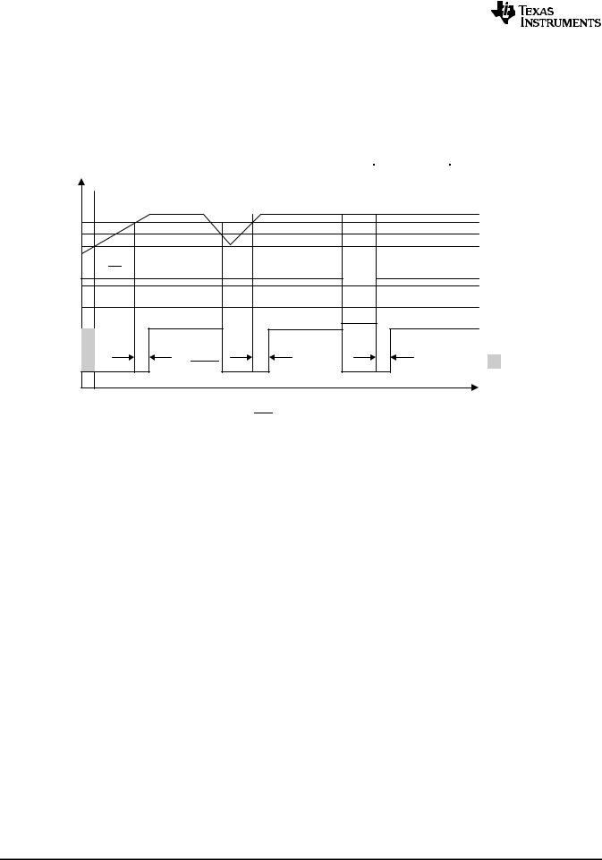
|
VDD |
|
|
VIT- + VHYS |
|
|
|
VIT- |
|
|
|
0.6 V |
|
|
|
MR |
|
|
|
0.7VDD |
|
|
|
0.3VDD |
|
|
|
|
|
|
TD = RESET DELAY |
TD |
TD |
TD |
= UNDEFINED STATE |
|
RESET |
|
|
TIME
Figure 1. MR and VDD Reset Timing
8 |
Submit Documentation Feedback |
Copyright © 2012–2015, Texas Instruments Incorporated |

TPS3831, TPS3839
www.ti.com |
SBVS193D –JUNE 2012–REVISED JULY 2015 |
7.7 Typical Characteristics
At TA = 25°C and C1 = 0.1 µF, unless otherwise noted. |
|
|
|
|
|
|
|
|
|||||
|
200 |
VDD = 1.2 V |
|
|
|
|
|
220 |
|
|
|
|
|
|
190 |
|
|
|
|
|
|
|
|
|
TPS3839K33 |
||
|
VDD = 3.3 V |
|
|
|
|
|
|
|
|
|
|
|
|
|
|
|
|
|
|
|
|
|
|
|
|
|
|
|
180 |
VDD = 5.0 V |
|
|
|
|
Reset Delay Time (ms) |
210 |
|
|
|
|
|
Supply Current (nA) |
170 |
VDD = 6.5 V |
|
|
|
|
|
|
|
|
|
||
|
|
|
|
|
|
|
|
|
|
|
|||
160 |
|
|
|
|
|
|
|
|
|
|
|
||
150 |
|
|
|
|
|
200 |
|
|
|
|
|
||
140 |
|
|
|
|
|
|
|
|
|
|
|
||
130 |
|
|
|
|
|
190 |
|
|
|
|
|
||
120 |
|
|
|
|
|
|
|
|
|
|
|||
|
|
|
|
|
|
|
|
|
|
|
|
|
|
|
110 |
|
|
|
|
|
|
|
|
|
|
|
|
|
100 |
−15 |
10 |
35 |
60 |
85 |
|
180 |
−15 |
10 |
35 |
60 |
85 |
|
−40 |
|
−40 |
||||||||||
|
|
|
Temperature (°C) |
|
G001 |
|
|
|
Temperature (°C) |
|
G002 |
||
|
|
|
|
|
|
|
|
|
|
|
|
||
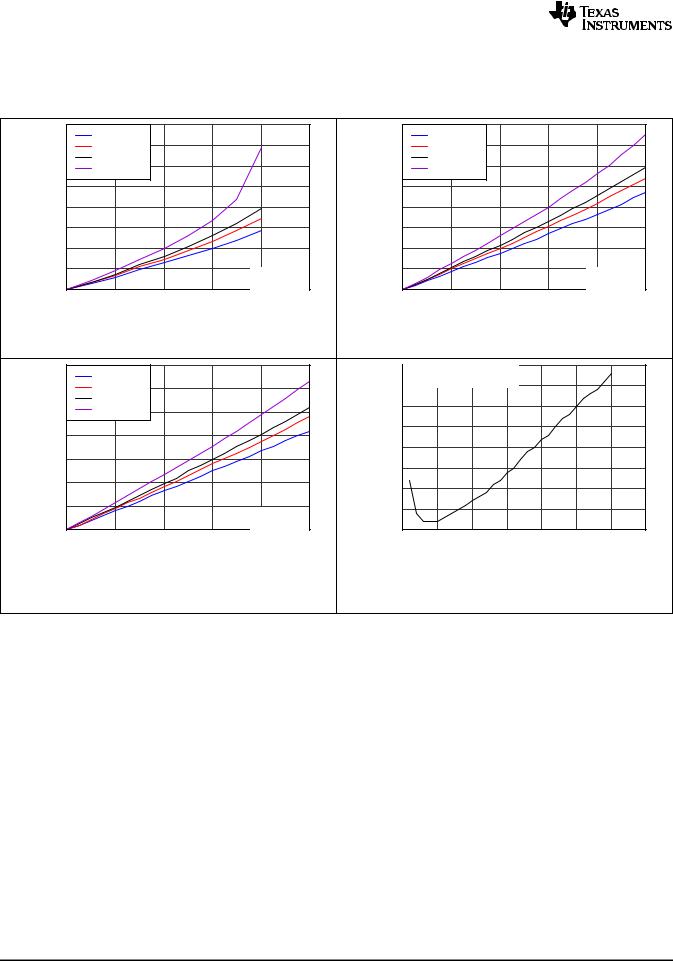
Figure 2. Supply Current vs Temperature |
Figure 3. Reset Delay vs Temperature |
|
0.2 |
|
|
|
|
|
|
1.8 |
|
|
|
|
|
VDD = 1.8 V |
|
|
|
|
|
|
|
|
|
|
|
|
|
|
|
||
|
0 |
|
|
|
|
|
|
1.6 |
|
|
|
|
|
|
|
|
|
|
|
|
|
|
|
|
|
|
|
|
|
|
|
(%) |
−0.2 |
|
|
|
|
|
|
|
|
|
|
|
|
|
|
|
|
|
|
|
|
|
|
|
|
|
|
|
|
|
|
IT– |
|
|
|
|
|
|
(V) |
1.4 |
|
|
|
|
|
|
|
V |
−0.4 |
|
|
|
|
|
|
|
|
|
|
|
|
|
|
in |
|
|
|
|
|
OH |
|
|
|
|
|
|
|
|
|
|
|
|
|
|
|
|
|
|
|
|
|
|
|
||
Change |
|
|
|
|
|
|
V |
1.2 |
|
|
|
|
|
|
|
|
|
|
|
|
|
|
|
|
|
|
|
|
|
|
|
|
−0.6 |
|
|
|
|
|
|
|
TA = −40 °C |
|
|
|
|
|
|
|
|
|
|
|
|
|
|
|
|
|
|
|
|
||
|
−0.8 |
|
|
|
|
|
|
1 |
TA = 0°C |
|
|
|
|
|
|
|
|
|
|
TPS3839A09 |
|
|
TA = +25°C |
|
|
|
|
|
|||
|
|
|
|
|
|
|
|
|
|
|
|
||||
|
|
|
|
|
TPS3839K50 |
|
|
TA = +85°C |
|
|
|
|
|
||
|
−1 |
−15 |
10 |
35 |
60 |
85 |
|
0.8 |
0.5 |
1 |
1.5 |
2 |
2.5 |
3 |
3.5 |
|
−40 |
|
0 |
||||||||||||
|
|
|
Temperature (°C) |
|
G003 |
|
|
|
|
IOH (mA) |
|
|
G004 |
||
Figure 4. Threshold Voltage vs Temperature |
Figure 5. VOH vs IOH and Temperature for VDD = 1.8 V |
3.5 |
|
|
|
VDD = 3.3 V |
|
4 |
|
|
|
|
VDD =4.0 V |
||
|
|
|
|
|
|
|
|
|
|
||||
|
|
|
|
|
|
|
3.5 |
|
|
|
|
|
|
2.5 |
|
|
|
|
|
|
|
|
|
|
|
|
|
(V) |
|
|
|
|
|
(V) |
3 |
|
|
|
|
|
|
OH |
|
|
|
|
|
OH |
|
|
|
|
|
|
|
|
|
|
|
|
|
|
|
|
|
|
|
||
V |
|
|
|
|
|
V |
|
|
|
|
|
|
|
1.5 |
TA = −40 °C |
|
|
|
|
|
|
TA = −40 °C |
|
|
|
|
|
|
|
|
|
|
|
2.5 |
|
|
|
|
|||
|
TA = 0°C |
|
|
|
|
|
|
TA = 0°C |
|
|
|
|
|
|
TA = +25°C |
|
|
|
|
|
|
TA = +25°C |
|
|
|
|
|
|
TA = +85°C |
|
|
|
|
|
|
TA = +85°C |
|
|
|
|
|
0.5 |
2 |
4 |
6 |
8 |
10 |
|
2 |
2 |
4 |
6 |
8 |
10 |
12 |
0 |
|
0 |
|||||||||||
IOH (mA) |
G005 |
IOH (mA) |
G006 |
Figure 6. VOH vs IOH and Temperature for VDD = 3.3 V |
Figure 7. VOH vs IOH and Temperature for VDD = 4.0 V |
Copyright © 2012–2015, Texas Instruments Incorporated |
Submit Documentation Feedback |
9 |
TPS3831, TPS3839
SBVS193D –JUNE 2012 –REVISED JULY 2015 |
www.ti.com |
Typical Characteristics (continued)
At TA = 25°C and C1 = 0.1 µF, unless otherwise noted. |
|
|
|
|
|
|
|
|
|||||
|
1.6 |
TA = −40 °C |
|
|
|
|
|
1.6 |
TA = −40 °C |
|
|
|
|
|
|
|
|
|
|
|
|
|
|
|
|
||
|
1.4 |
TA = 0°C |
|
|
|
|
|
1.4 |
TA = 0°C |
|
|
|
|
|
1.2 |
TA = +25°C |
|
|
|
|
|
1.2 |
TA = +25°C |
|
|
|
|
|
TA = +25°C |
|
|
|
|
|
TA = +85°C |
|
|
|
|
||
(V) |
1 |
|
|
|
|
|
(V) |
1 |
|
|
|
|
|
0.8 |
|
|
|
|
|
0.8 |
|
|
|
|
|
||
OL |
|
|
|
|
|
OL |
|
|
|
|
|
||
|
|
|
|
|
|
|
|
|
|
|
|
||
V |
0.6 |
|
|
|
|
|
V |
0.6 |
|
|
|
|
|
|
|
|
|
|
|
|
|
|
|
|
|
||
|
0.4 |
|
|
|
|
|
|
0.4 |
|
|
|
|
|
|
0.2 |
|
|
|
VDD = 1.8 V |
|
|
0.2 |
|
|
|
VDD = 3.3 V |
|
|
|
|
|
|
|
|
|
|
|
|
|||
|
0 |
1 |
2 |
3 |
4 |
5 |
|
0 |
2 |
4 |
6 |
8 |
10 |
|
0 |
|
0 |
||||||||||
IOL (mA) |
G007 |
IOL (mA) |
G008 |
Figure 8. VOL vs IOL and Temperature for VDD = 1.8 V |
Figure 9. VOL vs IOL and Temperature for VDD = 3.3 V |
|
1.4 |
TA = −40 °C |
|
|
|
|
(µs) |
50 |
|
|
|
|
|
|
|
|
|
|
|
|
|
|
|
|
|
|
|
|
|||
|
|
|
|
|
|
Reset |
|
Reset Occurs Above Line |
|
|
|
|
|||
|
|
TA = +25°C |
|
|
|
|
|
|
|
|
|
|
|
|
|
|
1.2 |
TA = 0°C |
|
|
|
|
|
45 |
|
|
|
|
|
|
|
(V) |
1 |
TA = +85°C |
|
|
|
|
Trigger |
40 |
|
|
|
|
|
|
|
|
|
|
|
|
|
|
|
|
|
|
|
|
|||
|
|
|
|
|
|
|
|
|
|
|
|
|
|
|
|
|
0.8 |
|
|
|
|
|
|
35 |
|
|
|
|
|
|
|
V |
|
|
|
|
|
Duration |
|
|
|
|
|
|
|
|
|
|
|
|
|
|
|
30 |
|
|
|
|
|
|
|
||
OL |
|
|
|
|
|
|
|
|
|
|
|
|
|
|
|
0.6 |
|
|
|
|
|
|
|
|
|
|
|
|
|
|
|
|
|
|
|
|
|
|
25 |
|
|
|
|
|
|
|
|
|
|
|
|
|
|
|
Pulse |
|
|
|
|
|
|
|
|
|
0.4 |
|
|
|
|
|
20 |
|
|
|
|
|
|
|
|
|
|
|
|
|
|
|
|
|
|
|
|
|
|
||
|
|
|
|
|
|
|
Minimum |
|
|
|
|
|
|
|
|
|
0 |
|
|
|
|
|
10 |
|
|
|
|
|
|
|
|
|
0.2 |
|
|
|
|
|
|
15 |
|
|
|
|
|
|
|
|
|
|
|
|
VDD = 4.0 V |
|
|
|
|
|
|
|
|
||
|
|
|
|
|
|
|
|
|
|
|
|
|
|
||
|
0 |
2 |
4 |
6 |
8 |
10 |
|
0 |
5 |
10 |
15 |
20 |
25 |
30 |
35 |
|
|
|
|
IOL (mA) |
|
G009 |
|
|
|
VDD voltage drop below VIT− |
(%) |
|
G010 |
||
Figure 10. VOL vs IOL and Temperature for VDD = 4.0 V |
Figure 11. Maximum Pulse Duration vs Percent of |
Threshold Overdrive
10 |
Submit Documentation Feedback |
Copyright © 2012–2015, Texas Instruments Incorporated |
Loading...