


TMX320C44PDB50
Texas Instruments TMX320C44PDB50, TMS320C44PDB60, TMS320C44PDB50, TMS320C44GFWA, TMS320C44GFW60 Datasheet
...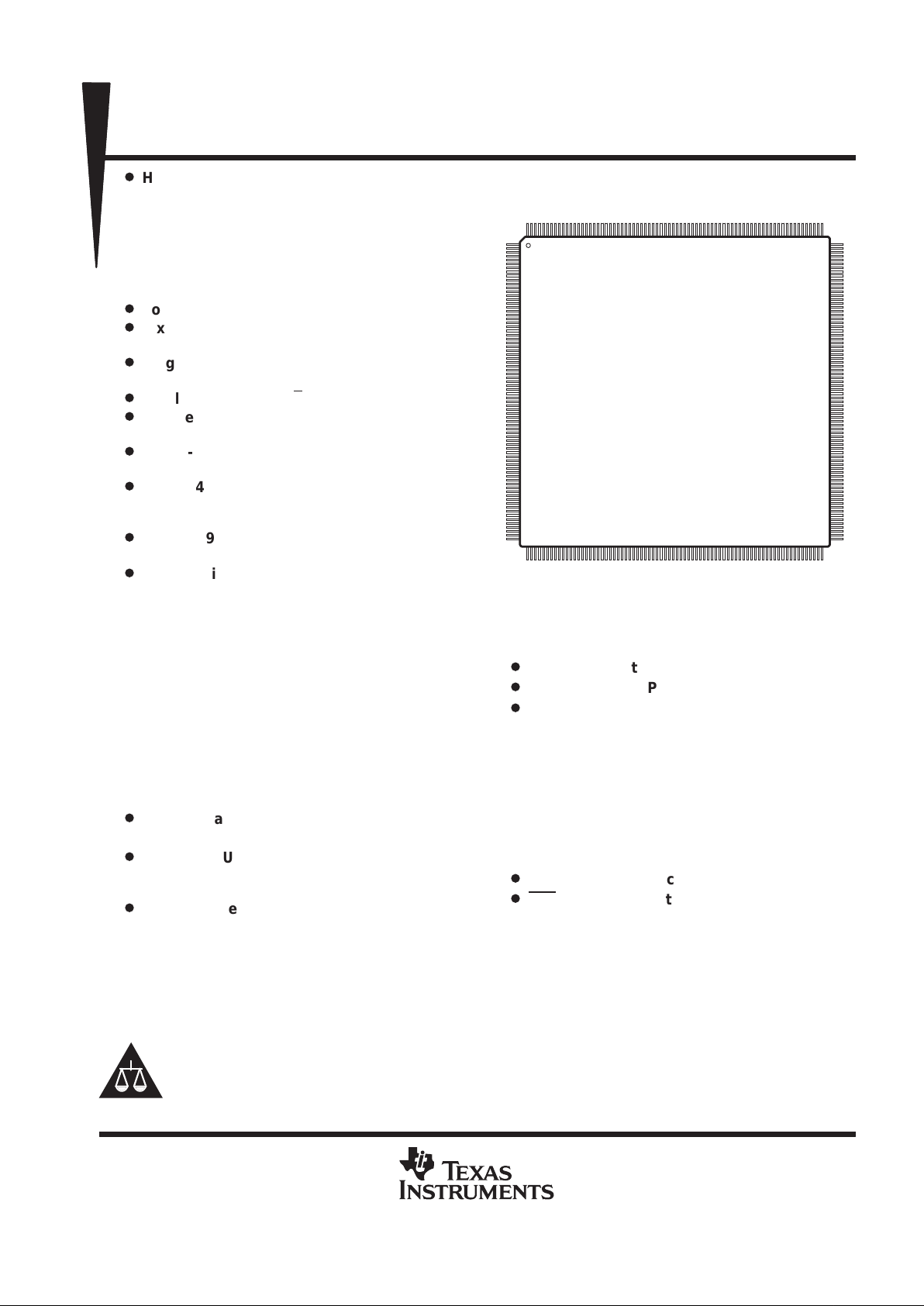
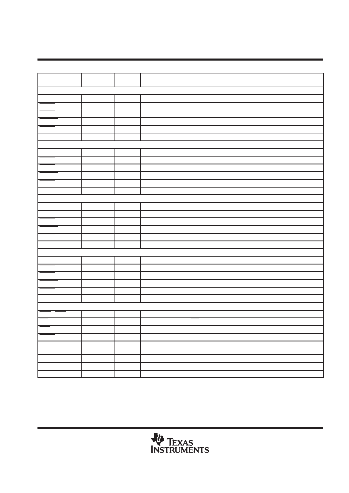
PDB PACKAGE
(TOP VIEW)
‡
‡
See Pin Assignments table and Pin Functions table for location
and description of all pins.
76
1
304
77 152
153
228
229
TMS320C44
DIGITAL SIGNAL PROCESSOR
SPRS031B – AUGUST 1994 – REVISED DECEMBER 1995
1
POST OFFICE BOX 1443 • HOUSTON, TEXAS 77251–1443
D
Highest Performance Floating-Point Digital
Signal Processor (DSP)
– TMS320C44-60:
33-ns Instruction Cycle Time,
330 MOPS, 60 MFLOPS,
30 MIPS, 336M Bytes/s
– TMS320C44-50:
40-ns Instruction Cycle Time
D
Four Communication Ports
D
Six-Channel Direct Memory Address (DMA)
Coprocessor
D
Single-Cycle Conversion to and From
IEEE-754 Floating-Point Format
D
Single Cycle, 1/x, 1/√x
D
Source-Code Compatible With ’320C3x and
’320C4x
D
Single-Cycle 40-Bit Floating-Point,
32-Bit Integer Multipliers
D
Twelve 40-Bit Registers, Eight Auxiliary
Registers, 14 Control Registers,
and Two Timers
D
IEEE-1149.1
†
(JTAG) Boundary-Scan
Compatible
D
Two Identical External Data and Address
Buses Supporting Shared Memory
Systems and High Data-Rate,
Single-Cycle Transfers
– High Port-Data Rate of 120M Bytes/s
(TMS320C44-60) (Each Bus)
– 128M-Byte Program/Data/Peripheral
Address Space
– Memory-Access Request for Fast,
Intelligent Bus Arbitration
– Separate Address-Bus, Data-Bus, and
Control-Enable Pins
– Four Sets of Memory-Control Signals
Support Different Speed Memories in
Hardware
D
304-Pin Plastic Quad Flatpack
(PDB Suffix)
D
Fabricated Using 0.72-µm Enhanced
Performance Implanted CMOS (EPIC)
Technology by Texas Instruments (TI)
D
Separate Internal Program-, Data-, and
DMA-Coprocessor Buses for Support of
Massive Concurrent I/O of Program and
Data, Thereby Maximizing Sustained CPU
Performance
D
IDLE2 Clock-Stop Power-Down Mode
D
Communication-Port-Direction Pin
D
On-Chip Program Cache and
Dual-Access/Single-Cycle RAM for
Increased Memory-Access Performance
– 512-Byte Instruction Cache
– 8K Bytes of Single-Cycle Dual-Access
Program or Data RAM
– ROM-Based Boot Loader Supports
Program Bootup Using 8-, 16-, or 32-Bit
Memories or One of the Communication
Ports
D
Software-Communication-Port Reset
D
NMI With Bus-Grant Feature
Please be aware that an important notice concerning availability, standard warranty, and use in critical applications of
Texas Instruments semiconductor products and disclaimers thereto appears at the end of this data sheet.
PRODUCTION DATA information is current as of publication date.
Products conform to specifications per the terms of Texas Instruments
standard warranty. Production processing does not necessarily include
testing of all parameters.
Copyright 1995, Texas Instruments Incorporated
†
IEEE Standard 1149.1–1990 Standard Test-Access Port and Boundary-Scan Architecture
EPIC and TI are trademarks of Texas Instruments Incorporated.
TMS320C44
DIGITAL SIGNAL PROCESSOR
SPRS031B – AUGUST 1994 – REVISED DECEMBER 1995
2
POST OFFICE BOX 1443 • HOUSTON, TEXAS 77251–1443
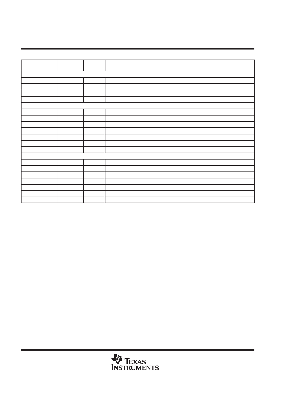
block diagram
32 32
32 32 32 32 32 32
D31–D0
A23–A0
DE
AE
STAT3 – STAT0
LOCK
STRB0, STRB1
R/W0, R/W1
PAGE0, PAGE1
RDY0
, RDY1
CE0, CE1
IR
PC
X1
X2/CLKIN
ROMEN
RESET
RESETLOC0,
RESETLOC1
NMI
IIOF(3–0)
IACK
H1
H3
CV
SS
DV
DD
DV
SS
IV
SS
DV
DD
DV
DD
V
DDL
V
SSL
V
SUBS
32 3232 32
40 40
40
40
32-Bit Barrel
Shifter
40
40
ALU
Extended
Precision
Registers
(R0–R11)
40
40
32
40
40
ARAU0 ARAU1
BK
Auxiliary
Registers
(AR0–AR7)
Other
Registers
(14)
CPU1
CPU2
32
32
32
32
32
32
32
32
32
32
REG1
32
R
E
G
1
Multiplier
Continued on next page
REG2
REG 1
Controller
PDATA Bus
DMADATA Bus
DDATA Bus
DADDR 1 Bus
DADDR 2 Bus
PADDR Bus
DMAADDR Bus
DISP, IR0, IR1
CPU1
REG2
Cache
(512 bytes)
RAM Block 0
(4K bytes)
RAM Block 1
(4K bytes)
ROM Block
(reserved)
MUX
MUX
REG1
TMS320C44
DIGITAL SIGNAL PROCESSOR
SPRS031B – AUGUST 1994 – REVISED DECEMBER 1995
3
POST OFFICE BOX 1443 • HOUSTON, TEXAS 77251–1443
block diagram (continued)
LD31– LD0
LA23–LA0
LDE
LAE
LSTAT3– LSTAT0
LLOCK
LSTRB0, LSTRB1
LR/W0, LR/W1
LPAGE0, LPAGE1
LRDY0
, LRDY1
LCE0, LCE1
DMA Channel 1
DMA Channel 2
DMA Channel 4
DMA Channel 5
DMA Coprocessor
Six DMA Channels
3232
Global
Local
Port Control
Global-Control Register
Time-Period Register
Timer 1
Timer-Counter Register
TCLK1
Global-Control Register
Time-Period Register
Timer 0
Timer-Counter Register
TCLK0
Port-Control Registers
Output
FIFO
Input
FIFO
PAU
COM Port 1
CREQ1
CACK1
CSTRB1
CRDY1
C1D7–C1D0
Continued from previous page
Port-Control Registers
Output
FIFO
Input
FIFO
PAU
COM Port 5
CREQ5
CACK5
CSTRB5
CRDY5
C5D7–C5D0
DDATA Bus
DADDR 1 Bus
DADDR 2 Bus
PADDR Bus
PDATA Bus
COM Port 2
COM Port 4
Four
Communication
Ports
†
DMADATA Bus
DMAADDR Bus
MUX
MUX
Peripheral Data Bus
Peripheral Address Bus
DMA Channel 0
DMA Channel 3
CDIR1
CDIR5
†
Communication ports 0 and 3 are not connected.
TMS320C44
DIGITAL SIGNAL PROCESSOR
SPRS031B – AUGUST 1994 – REVISED DECEMBER 1995
4
POST OFFICE BOX 1443 • HOUSTON, TEXAS 77251–1443
functions
This section lists signal descriptions for the ’320C44 device: each signal, number of pins, operating mode(s)
(that is, input, output, or high-impedance state as indicated by I, O, or Z, respectively), and function. The signals
are grouped according to function.
Pin Functions
SIGNAL NAME
NO. OF
PINS
TYPE
†
DESCRIPTION
GLOBAL-BUS EXTERNAL INTERFACE (73 pins)
D31–D0 32 I/O/Z 32-bit data port of the global-bus external interface
DE 1 I Data-bus-enable signal for the global-bus external interface
A23–A0 24 O/Z 24-bit address port of the global-bus external interface
AE 1 I Address-bus-enable signal for the global-bus external interface
STAT3–STAT0 4 O Status signals for the global-bus external interface
LOCK 1 O Lock signal for the global-bus external interface
STRB0
‡
1 O/Z Access strobe 0 for the global-bus external interface
R/W0
‡
1 O/Z Read/write signal for STRB0 accesses
PAGE0
‡
1 O/Z Page signal for STRB0 accesses
RDY0
‡
1 I Ready signal for STRB0 accesses
CE0
‡
1 I Control enable for the STRB0, PAGE0, and R/W0 signals
STRB1
‡
1 O/Z Access strobe 1 for the global-bus external interface
R/W1
‡
1 O/Z Read/write signal for STRB1 accesses
PAGE1
‡
1 O/Z Page signal for STRB1 accesses
RDY1
‡
1 I Ready signal for STRB1 accesses
CE1
‡
1 I Control enable for the STRB1, PAGE1, and R/W1 signals
LOCAL-BUS EXTERNAL INTERFACE (73 pins)
LD31–LD0 32 I/O/Z 32-bit data port of the local-bus external interface
LDE 1 I Data-bus-enable signal for the local-bus external interface
LA23–LA0 24 O/Z 24-bit address port of the local-bus external interface
LAE 1 I Address-bus-enable signal for the local-bus external interface
LSTAT3–LSTAT0 4 O Status signals for the local-bus external interface
LLOCK 1 O Lock signal for the local-bus external interface
LSTRB0
‡
1 O/Z Access strobe 0 for the local-bus external interface
LR/W0 1 O/Z Read/write signal for LSTRB0 accesses
LPAGE0 1 O/Z Page signal for LSTRB0 accesses
LRDY0 1 I Ready signal for LSTRB0 accesses
LCE0 1 I Control enable for the LSTRB0, LPAGE0, and LR/ W0 signals
LSTRB1
‡
1 O/Z Access strobe 1 for the local-bus external interface
LR/W1 1 O/Z Read/write signal for LSTRB1 accesses
LPAGE1 1 O/Z Page signal for LSTRB1 accesses
LRDY1 1 I Ready signal for LSTRB1 accesses
LCE1 1 I Control enable for the LSTRB1, LPAGE1, and LR/W1 signals
†
I = input, O = output, Z = high impedance
‡
The effective address range is defined by the local/global STRB
ACTIVE bits in the memory interface-control registers.
TMS320C44
DIGITAL SIGNAL PROCESSOR
SPRS031B – AUGUST 1994 – REVISED DECEMBER 1995
5
POST OFFICE BOX 1443 • HOUSTON, TEXAS 77251–1443
Pin Functions (Continued)
SIGNAL NAME
NO. OF
PINS
TYPE
†
DESCRIPTION
COMMUNICATION PORT 1 INTERFACE (13 pins)
C1D7–C1D0 8 I/O Communication port 1 data bus
CREQ1 1 I/O Communication port 1 token-request signal
CACK1 1 I/O Communication port 1 token-request-acknowledge signal
CSTRB1 1 I/O Communication port 1 data-strobe signal
CRDY1 1 I/O Communication port 1 data-ready signal
CDIR1 1 O Communication port 1 direction signal
COMMUNICATION PORT 2 INTERFACE (13 pins)
C2D7–C2D0 8 I/O Communication port 2 data bus
CREQ2 1 I/O Communication port 2 token-request signal
CACK2 1 I/O Communication port 2 token-request-acknowledge signal
CSTRB2 1 I/O Communication port 2 data-strobe signal
CRDY2 1 I/O Communication port 2 data-ready signal
CDIR2 1 O Communication port 2 direction signal
COMMUNICATION PORT 4 INTERFACE (13 pins)
C4D7–C4D0 8 I/O Communication port 4 data bus
CREQ4 1 I/O Communication port 4 token-request signal
CACK4 1 I/O Communication port 4 token-request-acknowledge signal
CSTRB4 1 I/O Communication port 4 data-strobe signal
CRDY4 1 I/O Communication port 4 data-ready signal
CDIR4 1 O Communication port 4 direction signal
COMMUNICATION PORT 5 INTERFACE (13 pins)
C5D7–C5D0 8 I/O Communication port 5 data bus
CREQ5 1 I/O Communication port 5 token-request signal
CACK5 1 I/O Communication port 5 token-request-acknowledge signal
CSTRB5 1 I/O Communication port 5 data-strobe signal
CRDY5 1 I/O Communication port 5 data-ready signal
CDIR5 1 O Communication port 5 direction signal
INTERRUPTS, I/O FLAGS, RESET, TIMER (12 pins)
IIOF3–IIOF0 4 I/O Interrupt and I/O flags
NMI 1 I Nonmaskable interrupt. NMI is sensitive to a low-going edge.
IACK 1 O Interrupt acknowledge
RESET 1 I Reset signal
RESETLOC1
RESETLOC0
2 I Reset-vector location
ROMEN 1 I On-chip ROM enable (0 = disable, 1 = enable)
TCLK0 1 I/O Timer 0
TCLK1 1 I/O Timer 1
†
I = input, O = output, Z = high impedance
TMS320C44
DIGITAL SIGNAL PROCESSOR
SPRS031B – AUGUST 1994 – REVISED DECEMBER 1995
6
POST OFFICE BOX 1443 • HOUSTON, TEXAS 77251–1443
Pin Functions (Continued)
SIGNAL NAME
NO. OF
PINS
TYPE
†
DESCRIPTION
CLOCK (4 pins)
X1 1 O Crystal
X2 / CLKIN 1 I Crystal/oscillator
H1 1 O H1 clock
H3 1 O H3 clock
POWER (71 pins)
CV
SS
17 I Ground
DV
SS
17 I Ground
IV
SS
6 I Ground
DV
DD
22 I 5-V
DC
supply
VSUBS 1 I Substrate (tie to ground)
V
DDL
4 I 5-V
DC
supply
V
SSL
4 I Ground
EMULATION (7 pins)
TCK 1 I IEEE 1149.1 test port clock
TDI 1 I IEEE 1149.1 test port data in
TDO 1 O/Z IEEE 1149.1 test port data out
TMS 1 I IEEE 1149.1 test port mode select
TRST 1 I IEEE 1149.1 test port reset
EMU0 1 I/O Emulation pin 0
EMU1 1 I/O Emulation pin 1
†
I = input, O = output, Z = high impedance
TMS320C44
DIGITAL SIGNAL PROCESSOR
SPRS031B – AUGUST 1994 – REVISED DECEMBER 1995
7
POST OFFICE BOX 1443 • HOUSTON, TEXAS 77251–1443
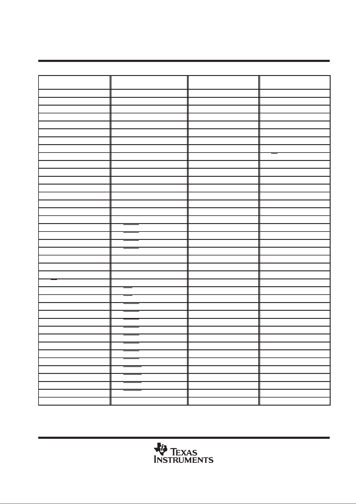
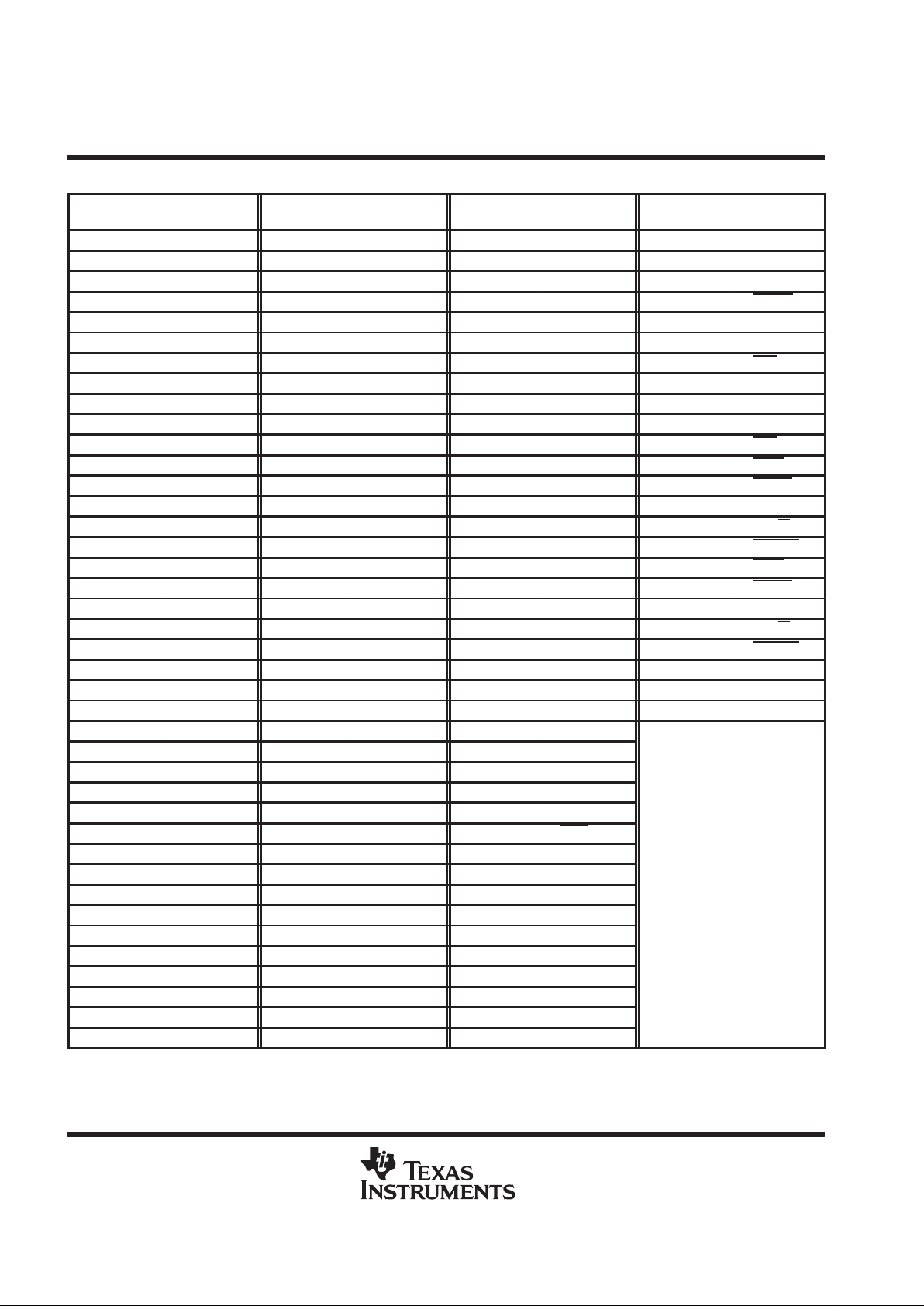
PDB Package Pin Assignments — Alphabetical Listing
PIN PIN PIN PIN
NAME NO. NAME NO. NAME NO. NAME NO.
A0 149 C2D7 34 CV
SS
134 D24 137
A1 150 C4D0 87 CV
SS
117 D25 138
A2 151 C4D1 88 CV
SS
102 D26 140
A3 152 C4D2 90 CV
SS
78 D27 141
A4 154 C4D3 92 CV
SS
62 D28 142
A5 155 C4D4 94 CV
SS
44 D29 143
A6 156 C4D5 97 CV
SS
25 D30 144
A7 157 C4D6 99 CV
SS
7 D31 145
A8 158 C4D7 100 CV
SS
282 DE 89
A9 159 C5D0 37 CV
SS
262 DV
DD
139
A10 160 C5D1 39 CV
SS
247 DV
DD
124
A11 162 C5D2 41 CV
SS
230 DV
DD
109
A12 165 C5D3 42 CV
SS
218 DV
DD
96
A13 166 C5D4 45 CV
SS
202 DV
DD
83
A14 167 C5D5 46 CV
SS
182 DV
DD
67
A15 168 C5D6 47 CV
SS
164 DV
DD
51
A16 169 C5D7 48 D0 104 DV
DD
40
A17 170 CACK1 13 D1 105 DV
DD
28
A18 171 CACK2 21 D2 106 DV
DD
17
A19 174 CACK4 73 D3 107 DV
DD
302
A20 175 CACK5 50 D4 108 DV
DD
288
A21 176 CDIR1 19 D5 110 DV
DD
272
A22 177 CDIR2 18 D6 111 DV
DD
256
A23 178 CDIR4 16 D7 112 DV
DD
244
AE 57 CDIR5 15 D8 113 DV
DD
236
C1D0 269 CE0 93 D9 114 DV
DD
223
C1D1 271 CE1 101 D10 115 DV
DD
207
C1D2 274 CRDY1 8 D11 118 DV
DD
188
C1D3 276 CRDY2 23 D12 120 DV
DD
172
C1D4 278 CRDY4 85 D13 122 DV
DD
161
C1D5 280 CRDY5 53 D14 123 DV
DD
153
C1D6 283 CREQ1 11 D15 125 DV
SS
147
C1D7 286 CREQ2 20 D16 127 DV
SS
133
C2D0 26 CREQ4 71 D17 128 DV
SS
116
C2D1 27 CREQ5 49 D18 129 DV
SS
103
C2D2 29 CSTRB1 14 D19 130 DV
SS
79
C2D3 30 CSTRB2 22 D20 131 DV
SS
63
C2D4 31 CSTRB4 84 D21 132 DV
SS
43
C2D5 32 CSTRB5 52 D22 135 DV
SS
24
C2D6 33 CV
SS
148 D23 136 DV
SS
6
TMS320C44
DIGITAL SIGNAL PROCESSOR
SPRS031B – AUGUST 1994 – REVISED DECEMBER 1995
8
POST OFFICE BOX 1443 • HOUSTON, TEXAS 77251–1443
PDB Package Pin Assignments — Alphabetical Listing (Continued)
PIN PIN PIN PIN
NAME NO. NAME NO. NAME NO. NAME NO.
DV
SS
281 LA17 253 LD30 228 STAT0 68
DV
SS
261 LA18 254 LD31 229 STAT1 66
DV
SS
246 LA19 255 LDE 291 STAT2 64
DV
SS
231 LA20 257 LLOCK 284 STAT3 61
DV
SS
217 LA21 258 LOCK 95 STRB0 58
DV
SS
201 LA22 259 LPAGE0 299 STRB1 69
DV
SS
179 LA23 260 LPAGE1 294 TCK 86
DV
SS
163 LAE 287 LRDY0 298 TCLK0 290
EMU0 75 LCE0 297 LRDY1 293 TCLK1 289
EMU1 74 LCE1 292 LR/W0 300 TDI 76
H1 266 LD0 183 LR/W1 295 TDO 80
H3 268 LD1 184 LSTAT0 279 TMS 82
IACK 270 LD2 185 LSTAT1 277 TRST 81
IIOF0 10 LD3 186 LSTAT2 275 V
DDL
38
IIOF1 9 LD4 187 LSTAT3 273 V
DDL
121
IIOF2 5 LD5 192 LSTRB0 301 V
DDL
191
IIOF3 4 LD6 194 LSTRB1 296 V
DDL
267
IV
SS
126 LD7 195 NC 1 V
SSL
36
IV
SS
65 LD8 196 NC 77 V
SSL
119
IV
SS
35 LD9 197 NC 173 V
SSL
193
IV
SS
2 LD10 200 NC 180 V
SSL
265
IV
SS
285 LD11 203 NC 181 VSUBS 146
IV
SS
209 LD12 204 NC 189 X1 264
LA0 232 LD13 205 NC 190 X2/CLKIN 263
LA1 233 LD14 206 NC 198
LA2 234 LD15 208 NC 199
LA3 235 LD16 210 NC 214
LA4 237 LD17 211 NC 303
LA5 238 LD18 212 NC 304
LA6 239 LD19 213 NMI 3
LA7 240 LD20 215 PAGE0 60
LA8 241 LD21 216 PAGE1 72
LA9 242 LD22 219 RDY0 91
LA10 243 LD23 220 RDY1 98
LA11 245 LD24 221 RESET 54
LA12 248 LD25 222 RESETLOC0 55
LA13 249 LD26 224 RESETLOC1 56
LA14 250 LD27 225 ROMEN 12
LA15 251 LD28 226 R/W0 59
LA16 252 LD29 227 R/W1 70

TMS320C44
DIGITAL SIGNAL PROCESSOR
SPRS031B – AUGUST 1994 – REVISED DECEMBER 1995
9
POST OFFICE BOX 1443 • HOUSTON, TEXAS 77251–1443
PDB Package Pin Assignments — Numerical Listing
PIN PIN PIN PIN
NO. NAME NO. NAME NO. NAME NO. NAME
1 NC 41 C5D2 81 TRST 121 V
DDL
2 IV
SS
42 C5D3 82 TMS 122 D13
3 NMI 43 DV
SS
83 DV
DD
123 D14
4 IIOF3 44 CV
SS
84 CSTRB4 124 DV
DD
5 IIOF2 45 C5D4 85 CRDY4 125 D15
6 DV
SS
46 C5D5 86 TCK 126 IV
SS
7 CV
SS
47 C5D6 87 C4D0 127 D16
8 CRDY1 48 C5D7 88 C4D1 128 D17
9 IIOF1 49 CREQ5 89 DE 129 D18
10 IIOF0 50 CACK5 90 C4D2 130 D19
11 CREQ1 51 DV
DD
91 RDY0 131 D20
12 ROMEN 52 CSTRB5 92 C4D3 132 D21
13 CACK1 53 CRDY5 93 CE0 133 DV
SS
14 CSTRB1 54 RESET 94 C4D4 134 CV
SS
15 CDIR5 55 RESETLOC0 95 LOCK 135 D22
16 CDIR4 56 RESETLOC1 96 DV
DD
136 D23
17 DV
DD
57 AE 97 C4D5 137 D24
18 CDIR2 58 STRB0 98 RDY1 138 D25
19 CDIR1 59 R/W0 99 C4D6 139 DV
DD
20 CREQ2 60 PAGE0 100 C4D7 140 D26
21 CACK2 61 STAT3 101 CE1 141 D27
22 CSTRB2 62 CV
SS
102 CV
SS
142 D28
23 CRDY2 63 DV
SS
103 DV
SS
143 D29
24 DV
SS
64 STAT2 104 D0 144 D30
25 CV
SS
65 IV
SS
105 D1 145 D31
26 C2D0 66 STAT1 106 D2 146 VSUBS
27 C2D1 67 DV
DD
107 D3 147 DV
SS
28 DV
DD
68 STAT0 108 D4 148 CV
SS
29 C2D2 69 STRB1 109 DV
DD
149 A0
30 C2D3 70 R/W1 110 D5 150 A1
31 C2D4 71 CREQ4 111 D6 151 A2
32 C2D5 72 PAGE1 112 D7 152 A3
33 C2D6 73 CACK4 113 D8 153 DV
DD
34 C2D7 74 EMU1 114 D9 154 A4
35 IV
SS
75 EMU0 115 D10 155 A5
36 V
SSL
76 TDI 116 DV
SS
156 A6
37 C5D0 77 NC 117 CV
SS
157 A7
38 V
DDL
78 CV
SS
118 D11 158 A8
39 C5D1 79 DV
SS
119 V
SSL
159 A9
40 DV
DD
80 TDO 120 D12 160 A10
TMS320C44
DIGITAL SIGNAL PROCESSOR
SPRS031B – AUGUST 1994 – REVISED DECEMBER 1995
10
POST OFFICE BOX 1443 • HOUSTON, TEXAS 77251–1443
PDB Package Pin Assignments — Numerical Listing (Continued)
PIN PIN PIN PIN
NO. NAME NO. NAME NO. NAME NO. NAME
161 DV
DD
201 DV
SS
241 LA8 281 DV
SS
162 A11 202 CV
SS
242 LA9 282 CV
SS
163 DV
SS
203 LD11 243 LA10 283 C1D6
164 CV
SS
204 LD12 244 DV
DD
284 LLOCK
165 A12 205 LD13 245 LA11 285 IV
SS
166 A13 206 LD14 246 DV
SS
286 C1D7
167 A14 207 DV
DD
247 CV
SS
287 LAE
168 A15 208 LD15 248 LA12 288 DV
DD
169 A16 209 IV
SS
249 LA13 289 TCLK1
170 A17 210 LD16 250 LA14 290 TCLK0
171 A18 211 LD17 251 LA15 291 LDE
172 DV
DD
212 LD18 252 LA16 292 LCE1
173 NC 213 LD19 253 LA17 293 LRDY1
174 A19 214 NC 254 LA18 294 LPAGE1
175 A20 215 LD20 255 LA19 295 LR / W1
176 A21 216 LD21 256 DV
DD
296 LSTRB1
177 A22 217 DV
SS
257 LA20 297 LCE0
178 A23 218 CV
SS
258 LA21 298 LRDY0
179 DV
SS
219 LD22 259 LA22 299 LPAGE0
180 NC 220 LD23 260 LA23 300 LR / W0
181 NC 221 LD24 261 DV
SS
301 LSTRB0
182 CV
SS
222 LD25 262 CV
SS
302 DV
DD
183 LD0 223 DV
DD
263 X2 / CLKIN 303 NC
184 LD1 224 LD26 264 X1 304 NC
185 LD2 225 LD27 265 V
SSL
186 LD3 226 LD28 266 H1
187 LD4 227 LD29 267 V
DDL
188 DV
DD
228 LD30 268 H3
189 NC 229 LD31 269 C1D0
190 NC 230 CV
SS
270 IACK
191 V
DDL
231 DV
SS
271 C1D1
192 LD5 232 LA0 272 DV
DD
193 V
SSL
233 LA1 273 LSTAT3
194 LD6 234 LA2 274 C1D2
195 LD7 235 LA3 275 LSTAT2
196 LD8 236 DV
DD
276 C1D3
197 LD9 237 LA4 277 LSTAT1
198 NC 238 LA5 278 C1D4
199 NC 239 LA6 279 LSTAT0
200 LD10 240 LA7 280 C1D5
TMS320C44
DIGITAL SIGNAL PROCESSOR
SPRS031B – AUGUST 1994 – REVISED DECEMBER 1995
11
POST OFFICE BOX 1443 • HOUSTON, TEXAS 77251–1443
memory map
Figure 1 shows the memory map for the ’320C44. Refer to the
TMS320C4x User’s Guide
(literature number
SPRU063B) for a detailed description of this memory mapping.
1 M
1 M
1 M
13 M
2 G–16 M
2 G–16 M
000000000h
000000FFFh
000001000h
0000FFFFFh
000100000h
0001000FFh
000100100h
0001FFFFFh
000200000h
0002FF7FFh
0002FF800h
0002FFBFFh
0002FFC00h
0002FFFFFh
000300000h
000FFFFFFh
01000000h
7FFFFFFFh
80000000h
80FFFFFh
81000000
FFFFFFFFh
Accessible Local Bus
(External)
Peripherals (Internal)
Reserved
Reserved
1K RAM BLK 0 (Internal)
1K RAM BLK 1 (Internal)
Local Bus
(External)
Local Bus
(alias region, see Figure 2)
Global Bus
(External)
Global Bus
(alias region, see Figure 2)
(a) INTERNAL ROM DISABLED
(ROMEN = 0)
Microprocessor Mode
Reserved
Peripherals (Internal)
Reserved
Reserved
1K RAM BLK 0 (Internal)
1K RAM BLK 1 (Internal)
Local Bus
(External)
Local Bus
(alias region, see Figure 2)
Global Bus
(External)
Global Bus
(alias region, see Figure 2)
(b) INTERNAL ROM ENABLED
(ROMEN = 1)
Microcomputer Mode
Boot-Loader ROM (Internal)
Structure Depends Upon
Romen Bit
Structure Identical
16 M
Figure 1. Memory Map for the ’320C44

TMS320C44
DIGITAL SIGNAL PROCESSOR
SPRS031B – AUGUST 1994 – REVISED DECEMBER 1995
12
POST OFFICE BOX 1443 • HOUSTON, TEXAS 77251–1443
description
The TMS320C44 DSP is a 32-bit, floating-point processor manufactured in 0.72-µm double-level-metal CMOS
technology. The TMS320C44 is part of the TMS320C4x generation of DSPs from Texas Instruments. The
on-chip parallel-processing capabilities of the ’C44 make the immense floating-point performance required by
many applications achievable.
operation
The ’320C44 has four on-chip communication ports for processor-to-processor communication with no external
hardware and simple communication software. This allows connectivity with no external-glue logic. The
communication ports remove input/output bottlenecks, and the independent smart 6-channel DMA
coprocessor is able to handle the CPU input/output burden.
T o fit the ’320C40 into a 304-pin PQFP package (thermally enhanced plastic quad flatpack), two communication
ports are removed and the external local and global address buses are reduced to 24 address lines each. In
this case, both the bond pads and driver circuits are removed, decreasing die size and power consumption.
Otherwise, functionality remains the same as the rest of the ’320C4x family.
The communication-port token and data-strobe control lines are internally connected to avoid spurious data,
boot-up, and power consumption problems.
TMS320C44
DIGITAL SIGNAL PROCESSOR
SPRS031B – AUGUST 1994 – REVISED DECEMBER 1995
13
POST OFFICE BOX 1443 • HOUSTON, TEXAS 77251–1443
memory aliasing
The ’320C44 offers global and local addresses of A0–A23 and LA0–LA23, giving an external address reach
of (2 buses) × (2
24
) = 2
25
words. Since the internal address span of the ’320C44 is 2
32
words, reading or writing
to memory outside of the base-address region causes memory aliasing. Figure 2 shows how the memory pages
overlap each other.
External Alias n
External Alias 1
External Alias 2
Local Bus
0x7F000000
0x02000000
0x02FFFFFF
0x01000000
0x7FFFFFFF
0x01FFFFFF
External Alias n
External Alias 1
External Alias 2
Global Bus
0xFF000000
0x82000000
0x82FFFFFF
0x81000000
0xFFFFFFFF
0x81FFFFFF
Base-Address
Region
0x00000000
0x00FFFFFF
Base-Address
Region
0x80000000
0x80FFFFFF
Figure 2. Memory Alias
central processing unit
The ’320C44 CPU is configured for high-speed internal parallelism for the highest sustained performance. The
key features of the CPU are:
D
Eight operations/cycle:
– 40-/32-bit floating-point/integer multiply
– 40-/32-bit floating-point/integer ALU operation
– Two data accesses
– Two address-register updates
D
Floating-point conversion
D
Divide and square-root support
D
’C3x and ’C4x assembly-language compatibility
D
Byte and halfword accessibility
 Loading...