


Texas Instruments TMS46400PDJ-80, TMS46400PDJ-70, TMS46400PDJ-60, TMS46400PDGA-80, TMS46400PDGA-70 Datasheet
...TMS44400, TMS44400P, TMS46400, TMS46400P 1048576-WORD BY 4-BIT DYNAMIC RANDOM-ACCESS MEMORIES
SMHS562C ± MAY 1995 ± REVISED NOVEMBER 1996
DOrganization . . . 1 048 576 × 4
DSingle 5-V Power Supply for TMS44400/P (±10% Tolerance)
DSingle 3.3-V Power Supply for TMS46400/P (±10% Tolerance)
DLow Power Dissipation (TMS46400P only) 200-mA CMOS Standby
200-mA Self Refresh
300-mA Extended-Refresh Battery
Backup
DPerformance Ranges:
|
ACCESS ACCESS ACCESS |
READ |
||
|
TIME |
TIME |
TIME |
OR WRITE |
|
(tRAC) (tCAC) |
(tAA) |
CYCLE |
|
|
(MAX) |
(MAX) |
(MAX) |
(MIN) |
'4x400/P-60 |
60 ns |
15 ns |
30 ns |
110 ns |
'4x400/P-70 |
70 ns |
18 ns |
35 ns |
130 ns |
'4x400/P-80 |
80 ns |
20 ns |
40 ns |
150 ns |
DEnhanced Page-Mode Operation for Faster Memory Access
DCAS-Before-RAS (CBR) Refresh
DLong Refresh Period
1024-Cycle Refresh in 16 ms
128 ms (MAX) for Low-Power, Self-Refresh Version (TMS4x400P)
D3-State Unlatched Output
DTexas Instruments EPIC CMOS Process
|
|
|
|
|
DGA PACKAGE |
|
|
|
|
|
|
|
DJ PACKAGE |
|
|
|
|||||||||||||||
|
|
|
|
|
|
( TOP VIEW ) |
|
|
|
|
|
|
|
|
( TOP VIEW ) |
|
|
|
|||||||||||||
DQ1 |
|
|
|
|
|
|
VSS |
|
DQ1 |
|
|
|
|
|
|
|
VSS |
||||||||||||||
|
1 |
|
26 |
|
|
|
|
1 |
|
|
26 |
|
|
||||||||||||||||||
|
|
|
|
|
|
|
|||||||||||||||||||||||||
DQ2 |
|
2 |
|
25 |
|
|
DQ4 |
|
DQ2 |
|
2 |
|
|
25 |
|
|
DQ4 |
||||||||||||||
|
|
|
|
|
|
|
|
|
|
|
|
|
|
|
DQ3 |
|
|
|
|
|
|
|
|
|
|
|
|
|
DQ3 |
||
|
|
W |
|
|
3 |
|
24 |
|
|
|
|
W |
|
|
3 |
|
|
24 |
|
|
|||||||||||
|
|
|
|
|
|
|
|
|
|
|
|
|
|
|
|
|
|
|
|
|
|
|
|
|
|
|
|
|
|
|
|
|
RAS |
|
|
4 |
|
23 |
|
|
CAS |
|
RAS |
|
|
4 |
|
|
23 |
|
|
CAS |
|||||||||||
|
A9 |
|
|
|
|
|
|
|
|
|
|
|
|
|
A9 |
|
|
|
|
|
|
|
|
|
|
||||||
|
|
5 |
|
22 |
|
|
OE |
|
|
|
5 |
|
|
22 |
|
|
OE |
|
|||||||||||||
|
A0 |
|
9 |
|
18 |
|
|
A8 |
|
A0 |
|
9 |
|
|
18 |
|
|
A8 |
|||||||||||||
|
|
|
|
|
|
|
|
|
|
|
|||||||||||||||||||||
|
A1 |
|
10 |
17 |
|
|
A7 |
|
A1 |
|
10 |
|
|
17 |
|
|
A7 |
||||||||||||||
|
|
|
|
|
|
|
|
|
|
||||||||||||||||||||||
|
A2 |
|
11 |
16 |
|
|
A6 |
|
A2 |
|
11 |
|
|
16 |
|
|
A6 |
||||||||||||||
|
|
|
|
|
|
|
|
|
|
||||||||||||||||||||||
|
A3 |
|
12 |
15 |
|
|
A5 |
|
A3 |
|
12 |
|
|
15 |
|
|
A5 |
||||||||||||||
|
|
|
|
|
|
|
|
|
|
||||||||||||||||||||||
|
VCC |
|
13 |
14 |
|
|
A4 |
|
VCC |
|
13 |
|
|
14 |
|
|
A4 |
||||||||||||||
|
|
|
|
|
|
|
|
|
|
||||||||||||||||||||||
|
|
|
|
|
|
||||||||||||||||||||||||||
|
|
|
|
|
|
|
|
|
|
|
|
|
|
|
|
|
|
|
|
|
|
|
|
|
|
|
|
|
|
|
|
|
|
|
|
|
|
|
|
|
|
|
|
|
PIN NOMENCLATURE |
|
|
|
|
|
|
||||||||||||
|
|
|
|
|
|
|
|
|
|
|
|
|
|
|
|
|
|
|
|
|
|
|
|
|
|
|
|
|
|
|
|
|
|
|
|
|
|
|
|
A0 ± A9 |
|
Address Inputs |
|
|
|
|
|
|
|||||||||||||||
|
|
|
|
|
|
|
|
|
|
|
|
|
|
|
Column-Address Strobe |
|
|
|
|||||||||||||
|
|
|
|
|
|
|
|
CAS |
|
|
|
|
|
|
|
|
|||||||||||||||
|
|
|
|
|
|
|
|
DQ1 ± DQ4 |
|
Data In |
|
|
|
|
|
|
|
|
|
|
|||||||||||
|
|
|
|
|
|
|
|
|
|
|
|
|
|
Output Enable |
|
|
|
|
|
|
|||||||||||
|
|
|
|
|
|
|
|
OE |
|
|
|
|
|
|
|
|
|
|
|
||||||||||||
|
|
|
|
|
|
|
|
RAS |
|
|
|
|
Row-Address Strobe |
|
|
|
|
|
|
||||||||||||
|
|
|
|
|
|
|
|
VCC |
|
5-V or 3.3-V Supply |
|
|
|
|
|
|
|||||||||||||||
|
|
|
|
|
|
|
|
VSS |
|
Ground |
|
|
|
|
|
|
|
|
|
|
|||||||||||
|
|
|
|
|
|
|
|
W |
|
|
|
|
Write Enable |
|
|
|
|
|
|
||||||||||||
|
|
|
|
|
|
|
|
|
|
|
|
|
|
|
|
|
|
|
|
|
|
|
|
|
|
|
|
|
|
|
|
D Operating Free-Air Temperature Range
0°C to 70°C
description
|
|
|
|
|
AVAILABLE OPTIONS |
|
||
The TMS4x400 series is a set of high-speed, |
|
|
|
|
||||
|
|
SELF-REFRESH |
|
|||||
4194304-bit dynamic random-access memories |
|
POWER |
REFRESH |
|||||
DEVICE |
BATTERY |
|||||||
(DRAMs), organized as 1048576 words of four |
SUPPLY |
CYCLES |
||||||
|
BACKUP |
|||||||
|
|
|
||||||
bits each. The TMS4x400P series is a set of |
|
|
|
|
||||
TMS44400 |
5 V |
Ð |
1024 in 16 ms |
|||||
high-speed, |
low-power, self-refresh with |
|||||||
TMS44400P |
5 V |
Yes |
1024 in 128 ms |
|||||
extended-refresh, |
4194304-bit |
DRAMs, |
||||||
TMS46400 |
3.3 V |
Ð |
1024 in 16 ms |
|||||
organized as 1048576 words of four bits each. |
||||||||
TMS46400P |
3.3 V |
Yes |
1024 in 128 ms |
|||||
Both series employ state-of-the-art |
enhanced |
|||||||
performance |
implanted CMOS |
(EPIC ) |
|
|
|
|
||
technology for high performance, reliability, and low power.
These devices feature maximum RAS access times of 60 ns, 70 ns, and 80 ns. All addresses and data-in lines are latched on chip to simplify system design. Data out is unlatched to allow greater system flexibility.
The TMS4x400 and TMS4x400P are offered in a 20/26-lead plastic small-outline (TSOP) package (DGA suffix) and a 300-mil 20/26-lead plastic surface-mount SOJ package (DJ suffix). Both packages are characterized for operation from 0°C to 70°C.
ADVANCE INFORMATION
Please be aware that an important notice concerning availability, standard warranty, and use in critical applications of Texas Instruments semiconductor products and disclaimers thereto appears at the end of this data sheet.
EPIC is a trademark of Texas Instruments Incorporated.
ADVANCE INFORMATION concerns new products in the sampling or preproduction phase of development. Characteristic data and other specifications are subject to change without notice.
POST OFFICE BOX 1443 •HOUSTON, TEXAS 77251±1443
Copyright 1996, Texas Instruments Incorporated
1

INFORMATION ADVANCE
TMS44400, TMS44400P, TMS46400, TMS46400P 1048576-WORD BY 4-BIT
DYNAMIC RANDOM-ACCESS MEMORIES
SMHS562C ± MAY 1995 ± REVISED NOVEMBER 1996
logic symbol²
|
9 |
RAM 1024K × 4 |
||
A0 |
20D10/21D0 |
|
||
10 |
|
|||
A1 |
|
|
||
11 |
|
|
||
A2 |
|
|
||
12 |
|
|
||
A3 |
|
|
||
14 |
|
|
||
A4 |
|
0 |
||
|
|
|||
A5 |
15 |
|
A 1 048 575 |
|
A6 |
16 |
|
|
|
17 |
|
|
||
A7 |
|
|
||
18 |
|
|
||
A8 |
|
|
||
5 |
|
|
||
A9 |
20D19/21D9 |
|
||
|
|
|||
|
|
C20 [ROW] |
|
|
|
4 |
G23/[REFRESH ROW] |
||
RAS |
24 [PWR DWN] |
|
||
|
|
|||
|
|
C21[COLUMN] |
||
|
23 |
G24 |
|
|
CAS |
& |
|
||
|
23C22 |
|||
|
|
|
||
W |
3 |
23,21D |
24,25 EN |
|
22 |
||||
OE |
G25 |
|
||
|
|
|||
DQ1 |
1 |
A,22D |
|
|
|
A,Z26 |
|||
|
|
26 |
||
|
2 |
|
||
DQ2 |
|
|
||
24 |
|
|
||
DQ3 |
|
|
||
25 |
|
|
||
DQ4 |
|
|
||
|
|
|
||
²This symbol is in accordance with ANSI / IEEE Std 91-1984 and IEC Publication 617-12. Pin numbers shown are for the DJ package.
functional block diagram
RAS CAS W OE
|
|
|
Timing and Control |
|
|
|
|
||
A0 |
|
8 |
Column Decode |
|
|
|
|
||
A1 |
|
|
|
|
|
||||
|
|
|
|
|
|
|
|
|
|
|
Column- |
2 |
Sense Amplifiers |
16 |
|
|
|
||
|
Address |
128K Array |
|
128K Array |
|
|
Data- |
|
|
|
|
|
|
|
|
||||
|
Buffers |
|
R |
|
|
|
|||
|
|
128K Array |
128K Array |
|
|
In |
|
||
A9 |
|
|
|
|
4 |
||||
|
|
o |
16 |
I/O |
Reg. |
||||
|
|
|
|
w |
|
|
Buffers |
|
|
|
|
|
|
|
|
|
|
|
|
|
|
16 |
|
D |
|
16 |
1 of 16 |
|
4 |
|
|
|
|
Selection |
Data- |
|
|||
|
Row- |
|
|
e |
|
|
|
|
|
|
|
|
|
|
|
Out |
|
||
|
Address |
10 |
|
c |
|
|
|
|
|
|
|
|
|
|
Reg. |
|
|||
|
Buffers |
|
o |
|
|
2 |
|
||
|
|
|
|
|
|
|
|||
|
|
|
|
d |
|
|
|
|
|
|
|
|
128K Array |
e |
128K Array |
|
|
|
DQ1 ± DQ4 |
|
|
|
|
|
|
|
|
|
|
|
|
|
10 |
|
|
|
|
|
|
2 |
POST OFFICE BOX 1443 •HOUSTON, TEXAS 77251±1443 |

TMS44400, TMS44400P, TMS46400, TMS46400P 1048576-WORD BY 4-BIT DYNAMIC RANDOM-ACCESS MEMORIES
SMHS562C ± MAY 1995 ± REVISED NOVEMBER 1996
operation
enhanced page mode
Enhanced-page-mode operation allows faster memory access by keeping the same row address while selecting random column addresses. The time for row-address setup and hold and address multiplex is eliminated. The maximum number of columns that can be accessed is determined by the maximum RAS low time and the CAS page cycle time used. With minimum CAS page cycle time, all 1024 columns specified by column addresses A0 through A9 can be accessed without intervening RAS cycles.
Unlike conventional page-mode DRAMs, the column-address buffers in this device are activated on the falling edge of RAS. The buffers act as transparent or flow-through latches while CAS is high. The falling edge of CAS latches the column addresses. This feature allows the TMS4x400 to operate at a higher data bandwidth than conventional page-mode parts because data retrieval begins as soon as the column address is valid rather than when CAS transitions low. This performance improvement is referred to as enhanced page mode. A valid column address can be presented immediately after row-address hold time has been satisfied, usually well in advance of the falling edge of CAS. In this case, data is obtained after tCAC maximum (access time from CAS low) if tAA maximum (access time from column address) has been satisfied. In the event that column addresses
for the next cycle are valid at the time CAS goes high, access time for the next cycle is determined by the later occurrence of tCAC (acces time from CAS low) or tCPA (access time from column precharge).
address (A0±A9)
Twenty address bits are required to decode any one of the 1048576 storage-cell locations. Ten row-address bits are set up on inputs A0 through A9 and latched onto the chip by RAS. The ten column-address bits are set up on A0 through A9 and latched onto the chip by CAS. All addresses must be stable on or before the falling edges of RAS and CAS. RAS is similar to a chip enable because it activates the sense amplifiers as well as the row decoder. CAS is used as a chip select, activating the output buffer, as well as latching the address bits into the column-address buffer.
write enable (W)
The read or write mode is selected through W input. A logic high on W selects the read mode and a logic low selects the write mode. W can be driven from standard TTL circuits (TMS44400/P) or low voltage TTL circuits (TMS46400/P) without a pullup resistor. The data input is disabled when the read mode is selected. When W goes low prior to CAS (early write), data out remains in the high-impedance state for the entire cycle, permitting a write operation independent of the state of OE. This permits early-write operation to complete with OE grounded.
data in/out (DQ1±DQ4)
Data out is the same polarity as data in. The output is in the high-impedance (floating) state until CAS and OE are brought low. In a read cycle, the output becomes valid after all access times are satisfied. The output remains valid while CAS and OE are low. CAS or OE going high returns the output to a high-impedance state. This is accomplished by bringing OE high prior to applying data, satisfying the OE to data delay hold time (tOED).
output enable (OE)
OE controls the impedance of the output buffers. When OE is high, the buffers remain in the high-impedance state. Bringing OE low during a normal cycle activates the output buffers, putting them in the low-impedance state. It is necessary for both RAS and CAS to be brought low for the output buffers to go into the low-impedance state. They remain in the low-impedance state until either OE or CAS is brought high.
ADVANCE INFORMATION
POST OFFICE BOX 1443 •HOUSTON, TEXAS 77251±1443 |
3 |

INFORMATION ADVANCE
TMS44400, TMS44400P, TMS46400, TMS46400P 1048576-WORD BY 4-BIT
DYNAMIC RANDOM-ACCESS MEMORIES
SMHS562C ± MAY 1995 ± REVISED NOVEMBER 1996
refresh
A refresh operation must be performed at least once every 16 ms (128 ms for TMS4x400P) to retain data. This can be achieved by strobing each of the 1024 rows (A0±A9). A normal read or write cycle refreshes all bits in each row that is selected. A RAS-only operation can be used by holding CAS at the high (inactive) level, conserving power as the output buffer remains in the high-impedance state. Externally generated addresses must be used for a RAS-only refresh. Hidden refresh can be performed while maintaining valid data at the output. This is accomplished by holding CAS at VIL after a read operation and cycling RAS after a specified
precharge period, similar to a RAS-only refresh cycle. The external address is ignored during the hidden-refresh cycle.
CAS-before-RAS (CBR) refresh
CBR refresh is utilized by bringing CAS low earlier than RAS (see parameter tCSR) and holding it low after RAS
falls (see parameter tCHR). For successive CBR refresh cycles, CAS can remain low while cycling RAS. The external address is ignored and the refresh address is generated internally.
A low-power battery-backup refresh mode that requires less than 300-mA (TMS46400P) or 500-mA (TMS44400P) refresh current is available on the low-power devices. Data integrity is maintained using CBR refresh with a period of 125 ms while holding RAS low for less than 1 ms. To minimize current consumption, all input levels need to be at CMOS levels (VIL ≤ 0.2 V, VIH ≥ VCC ± 0.2 V).
self refresh
The self-refresh mode is entered by dropping CAS low prior to RAS going low. CAS and RAS are both held low for a minimum of 100 ms. The chip is then refreshed by an on-board oscillator. No external address is required since the CBR counter is used to keep track of the address. To exit the self-refresh mode, both RAS and CAS are brought high to satisfy tCHS. Upon exiting the self-refresh mode, a burst refresh (refresh a full set of row addresses) must be executed before continuing with normal operation, to ensure that the DRAM is fully refreshed.
power up
To achieve proper device operation, an initial pause of 200 ms followed by a minimum of eight initialization cycles is required after full VCC level is achieved. These eight initialization cycles must include at least one refresh
(RAS-only or CBR) cycle.
test mode
The test mode is initiated with a CBR refresh cycle while simultaneously holding W low (WCBR). The entry cycle performs an internal refresh cycle while internally setting the device to perform parallel read or write on subsequent cycles. While in test mode, any desired data sequence can be performed on the device. The device exits test mode if a CBR refresh cycle with W held high or a RAS-only refresh (ROR) cycle is performed.
The TMS4x400/P is configured as a 512K × 8 bit device in test mode, where each DQ pin has a separate 2-bit parallel readand write-data bus. During a read cycle, the two internal bits are compared for each DQ pin separately. If the two bits agree, the DQ pin goes high; if not, the DQ pin goes low. The two bits are written to reflect the state of their respective DQ pins during a parallel-write operation. Each DQ pin is independent of the others, and any data pattern desired can be written on each DQ pin. Test time is reduced by a factor of 4 for this series.
4 |
POST OFFICE BOX 1443 •HOUSTON, TEXAS 77251±1443 |
|
TMS44400, TMS44400P, TMS46400, TMS46400P |
|
|
|
1048576-WORD BY 4-BIT |
|
|
DYNAMIC RANDOM-ACCESS MEMORIES |
|
|
SMHS562C ± MAY 1995 ± REVISED NOVEMBER 1996 |
test mode (continued) |
|
|
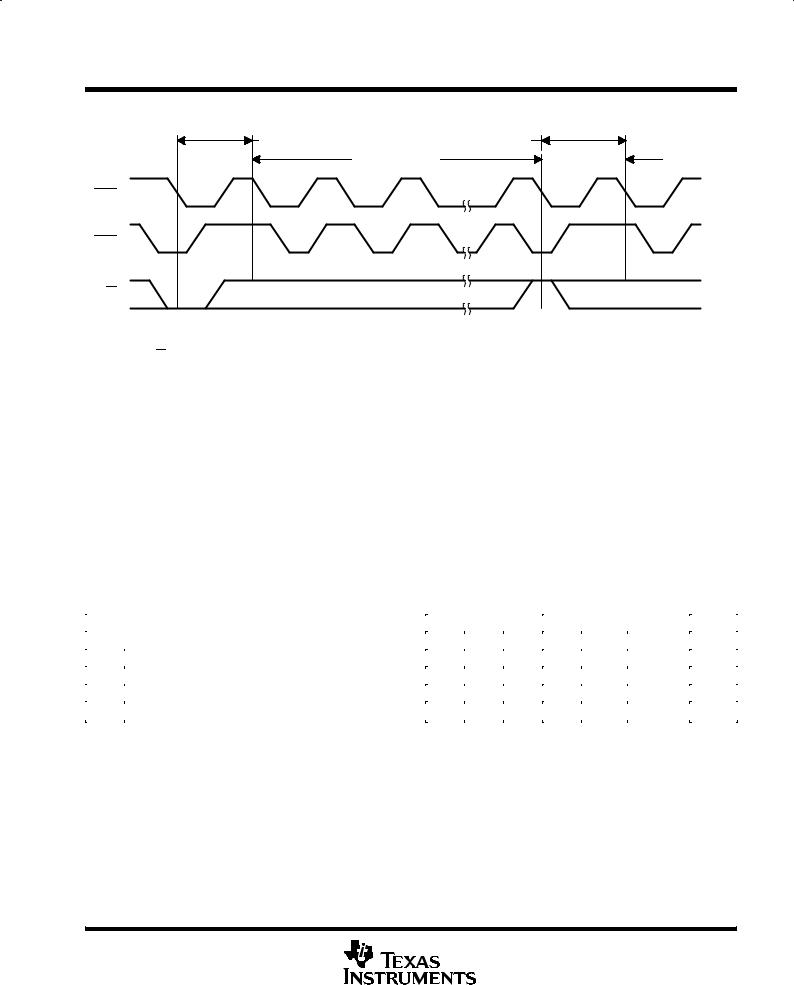
Entry Cycle |
|
Exit Cycle |
|
Test Mode Cycle |
Normal |
|
Mode |
|
|
|
|
RAS |
|
|
CAS
W
Figure 1. Test-Mode Cycle Timing²
² The states of W, data in, and address are defined by the type of cycle used during test mode.
absolute maximum ratings over operating free-air temperature range (unless otherwise noted)³
Supply voltage range, VCC: |
TMS44400, TMS44400P . . . . . . . . . . . . . . . . . . . . . . . |
± 1.0 V to 7.0 V |
|
TMS46400, TMS46400P . . . . . . . . . . . . . . . . . . . . . . . |
± 0.5 V to 4.6 V |
Voltage range on any pin (see Note 1) TMS44400, TMS44400P . . . . . . . . . . . . . . . . . . . . . . . |
± 1.0 V to 7.0 V |
|
|
TMS46400, TMS46400P . . . . . . . . . . . . . . . . . . . . . . . |
± 0.5 V to 4.6 V |
Short-circuit output current . . . . . . . . . . |
. . . . . . . . . . . . . . . . . . . . . . . . . . . . . . . . . . . . . . . . . . . . . . |
. . . . . . . . 50 mA |
Power dissipation . . . . . . . . . . . . . . . . . . |
. . . . . . . . . . . . . . . . . . . . . . . . . . . . . . . . . . . . . . . . . . . . . . |
. . . . . . . . . . 1 W |
Operating free-air temperature range, TA . . . . . . . . . . . . . . . . . . . . . . . . . . . . . . . . . . . . . . . . . . . . |
. . 0°C to 70°C |
|
Storage temperature range, Tstg . . . . . |
. . . . . . . . . . . . . . . . . . . . . . . . . . . . . . . . . . . . . . . . . . . . . |
± 55°C to 150°C |
³Stresses beyond those listed under ªabsolute maximum ratingsº may cause permanent damage to the device. These are stress ratings only, and functional operation of the device at these or any other conditions beyond those indicated under ªrecommended operating conditionsº is not
implied. Exposure to absolute-maximum-rated conditions for extended periods may affect device reliability. NOTE 1: All voltage values are with respect to VSS.
recommended operating conditions
|
|
TMS44400/ P |
|
TMS46400/ P |
UNIT |
|||
|
|
|
|
|
|
|
|
|
|
|
MIN |
NOM |
MAX |
MIN |
NOM |
MAX |
|
|
|
|
||||||
|
|
|
|
|
|
|
|
|
VCC |
Supply voltage |
4.5 |
5 |
5.5 |
3 |
3.3 |
3.6 |
V |
VIH |
High-level input voltage |
2.4 |
|
6.5 |
2 |
|
VCC + 0.3 |
V |
VIL |
Low-level input voltage (see Note 2) |
± 1 |
|
0.8 |
± 0.3 |
|
0.8 |
V |
TA |
Operating free-air temperature |
0 |
|
70 |
0 |
|
70 |
°C |
NOTE 2: |
The algebraic convention, where the more negative (less positive) limit is designated as minimum, is used for logic-voltage levels only. |
|||||||
ADVANCE INFORMATION
POST OFFICE BOX 1443 •HOUSTON, TEXAS 77251±1443 |
5 |

TMS44400, TMS44400P, TMS46400, TMS46400P 1048576-WORD BY 4-BIT
DYNAMIC RANDOM-ACCESS MEMORIES
SMHS562C ± MAY 1995 ± REVISED NOVEMBER 1996
electrical characteristics over recommended ranges of supply voltage and operating free-air temperature (unless otherwise noted)
|
|
|
|
|
|
|
|
TEST |
|
|
'44400 - 60 |
'44400 - 70 |
'44400 - 80 |
|
|||||
|
|
PARAMETER |
|
|
|
|
|
|
|
'44400P - 60 |
'44400P - 70 |
'44400P - 80 |
UNIT |
||||||
|
|
|
|
|
CONDITIONS |
|
|
||||||||||||
|
|
|
|
|
|
|
|
|
|
|
|||||||||
|
|
|
|
|
|
|
|
MIN |
MAX |
MIN MAX |
MIN MAX |
|
|||||||
|
|
|
|
|
|
|
|
|
|
|
|
|
|
|
|
||||
|
|
|
|
|
|
|
|
|
|
|
|
|
|
|
|
|
|
|
|
|
VOH |
High-level output voltage |
|
IOH = ± 5 mA |
|
|
|
|
|
|
|
2.4 |
|
2.4 |
2.4 |
V |
|||
|
VOL |
Low-level output voltage |
|
IOL = 4.2 mA |
|
|
|
|
|
|
|
|
0.4 |
0.4 |
0.4 |
V |
|||
|
|
|
|
VCC = 5.5 V, |
|
|
|
|
|
|
|
|
± 10 |
± 10 |
± 10 |
μA |
|||
|
II |
Input current (leakage) |
|
VI = 0 V to 6.5 V, |
|
|
|
||||||||||||
|
|
|
All others = 0 V to VCC |
|
|
|
|
|
|
|
|||||||||
|
IO |
Output current (leakage) |
|
VCC = 5.5 V, |
|
|
VO = 0 V to VCC, |
|
± 10 |
± 10 |
± 10 |
μA |
|||||||
|
|
|
|
|
|
|
|
|
|
|
|
|
|
||||||
|
|
CAS high |
|
|
|
|
|
|
|
|
|||||||||
|
|
|
|
|
|
|
|
|
|
|
|
|
|
|
|
||||
|
|
|
|
|
|
|
|
|
|
|
|
|
|
|
|
|
|
|
|
|
ICC1 |
Reador write-cycle current |
|
VCC = 5.5 V, |
|
|
Minimum cycle |
|
105 |
90 |
80 |
mA |
|||||||
|
(see Note 3) |
|
|
|
|
||||||||||||||
|
|
|
|
|
|
|
|
|
|
|
|
|
|
|
|
|
|
|
|
|
|
|
|
|
|
|
|
|
|
|
|
|
|
|
|
|
|
|
|
|
|
|
|
After one memory cycle, |
|
|
|
|
|
|
|
||||||||
|
|
|
|
RAS and CAS high, |
|
|
|
2 |
2 |
2 |
mA |
||||||||
ADVANCE |
|
|
|
VIH = 2.4 V ( TTL) |
|
|
|
|
|
|
|
||||||||
ICC3 |
(RAS only or CBR) |
|
CAS high (RAS only); |
|
|
|
105 |
90 |
80 |
mA |
|||||||||
|
ICC2 |
Standby current |
After one memory |
|
'44400 |
|
1 |
1 |
1 |
mA |
|||||||||
|
|
|
cycle, RAS and CAS |
|
|
|
|
|
|
|
|||||||||
|
|
|
|
high, |
|
|
|
|
|
|
|
|
|
|
|
|
|||
|
|
|
|
VIH = VCC ± 0.2 V |
|
'44400P |
|
500 |
500 |
500 |
μA |
||||||||
|
|
|
|
(CMOS) |
|
|
|
|
|
|
|
|
|
|
|
|
|||
|
|
|
|
|
|
|
|
|
|
|
|
|
|
|
|
|
|
|
|
|
|
Average refresh current |
|
VCC = 5.5 V, |
|
|
Minimum cycle, |
|
|
|
|
|
|||||||
|
|
|
RAS cycling, |
|
|
|
|
|
|
|
|
|
|
|
|
||||
|
|
|
|
|
|
|
|
|
|
|
|
|
|
|
|
||||
INFORMATION |
|
(see Note 4) |
|
|
|
|
|
|
|
|
|
|
|
|
|
|
|
|
|
|
|
RAS low after CAS low (CBR) |
|
|
|
|
|
||||||||||||
|
|
|
|
|
|
|
|
||||||||||||
|
|
|
|
|
|
|
|
|
|
|
|
|
|||||||
ICC10² |
(with CBR) |
|
0 V ≤ VIL ≤ 0.2 V, |
|
|
|
500 |
500 |
500 |
μA |
|||||||||
|
|
Average page |
|
VCC = 5.5 V, |
|
|
tPC = MIN, |
|
|
|
|
|
|||||||
|
ICC4 |
current |
|
RAS low, |
|
|
|
CAS cycling |
|
90 |
80 |
70 |
mA |
||||||
|
|
(see Notes 3 and 5) |
|
|
|
|
|
|
|
|
|
|
|
|
|
|
|
|
|
|
ICC6² |
Self-refresh current |
|
CAS |
≤ 0.2 V, |
|
|
|
RAS |
< 0.2 V, |
|
500 |
500 |
500 |
μA |
||||
|
|
(see Note 3) |
|
tRAS and tCAS > 1000 ms |
|
|
|
|
|
||||||||||
|
ICC7 |
Standby current, outputs |
|
RAS |
= VIH, |
|
|
|
CAS |
= VIL, |
|
5 |
5 |
5 |
mA |
||||
|
enabled (see Note 3) |
|
Data out = enabled |
|
|
|
|||||||||||||
|
|
|
|
|
|
|
|
|
|
||||||||||
|
|
|
|
|
|
|
|
|
|
|
|
|
|
||||||
|
|
|
|
tRC = 125 μs, |
|
|
|
tRAS ≤ 1 ms, |
|
|
|
|
|
||||||
|
|
Battery-backup current |
|
VCC ± 0.2 V ≤ VIH ≤ 6.5 V, |
|
|
|
|
|
||||||||||
|
|
|
|
|
|
|
|
|
|
|
|
|
|
|
|
|
|
|
|
|
|
|
|
|
|
|
|
|
|
|
|
||||||||
|
|
|
|
W |
and OE = VIH, |
|
|
|
|
|
|
|
|||||||
|
|
|
|
Address and data stable |
|
|
|
|
|
|
|
||||||||
|
|
|
|
|
|
|
|
|
|
|
|
|
|
|
|
|
|
|
|
|
² For TMS44400P only |
|
|
|
|
|
|
|
|
|
|
|
|
|
|
|
|
|
|
NOTES: 3. ICC MAX is specified with no load connected.
4.Measured with a maximum of one address change while RAS = VIL
5.Measured with a maximum of one address change while CAS = VIH
6 |
POST OFFICE BOX 1443 •HOUSTON, TEXAS 77251±1443 |
TMS44400, TMS44400P, TMS46400, TMS46400P 1048576-WORD BY 4-BIT DYNAMIC RANDOM-ACCESS MEMORIES
SMHS562C ± MAY 1995 ± REVISED NOVEMBER 1996
electrical characteristics over recommended ranges of supply voltage and operating free-air temperature (unless otherwise noted)
|
|
|
|
|
|
TEST |
|
'46400 - 60 |
|
'46400 - 70 |
|
'46400 - 80 |
|
|
|
||||||
PARAMETER |
|
|
|
|
|
'46400P - 60 |
'46400P - 70 |
'46400P - 80 |
UNIT |
|
|||||||||||
|
|
|
CONDITIONS |
|
|
||||||||||||||||
|
|
|
|
|
|
|
|
|
|
|
|||||||||||
|
|
|
|
|
|
MIN |
MAX |
MIN |
MAX |
MIN |
MAX |
|
|
||||||||
|
|
|
|
|
|
|
|
|
|
|
|
|
|
|
|
||||||
|
|
|
|
|
|
|
|
|
|
|
|
|
|
|
|
|
|
|
|
|
|
VOH |
High-level |
|
IOH = ± 2 mA (LVTTL) |
|
2.4 |
|
2.4 |
|
2.4 |
|
V |
|
|||||||||
output voltage |
|
|
|
|
μ |
|
|
|
|
|
VCC ± 0.2 |
|
VCC ± 0.2 |
|
VCC ± 0.2 |
|
|
||||
|
|
|
IOH = ± 100 A (LVCMOS) |
|
|
|
|
|
|||||||||||||
VOL |
Low-level |
|
IOL = 2 mA (LVTTL) |
|
|
0.4 |
|
0.4 |
|
0.4 |
V |
|
|||||||||
output voltage |
|
|
|
μ |
|
|
|
|
|
|
0.2 |
|
0.2 |
|
0.2 |
|
|||||
|
|
|
IOL = 100 A (LVCMOS) |
|
|
|
|
|
|
||||||||||||
II |
Input current |
|
VI = 0 V to 3.9 V, |
VCC = 3.6 V, |
|
± 10 |
|
± 10 |
|
± 10 |
μA |
|
|||||||||
(leakage) |
|
All others = 0 V to VCC |
|
|
|
|
|
||||||||||||||
|
|
|
|
|
|
|
|
|
|
|
|||||||||||
IO |
Output current |
|
VO = 0 V to VCC, VCC = 3.6 V, |
|
± 10 |
|
± 10 |
|
± 10 |
μA |
|
||||||||||
(leakage) |
|
|
|
|
|
|
|
|
|
|
|
|
|
|
|
|
|||||
|
CAS high |
|
|
|
|
|
|
|
|
|
|||||||||||
|
|
|
|
|
|
|
|
|
|
|
|
|
|
|
|||||||
|
|
|
|
|
|
|
|
|
|
|
|
|
|
|
|
|
|
|
|
|
|
|
Reador |
|
|
|
|
|
|
|
|
|
|
|
|
|
|
|
|
|
|
|
|
ICC1 |
write-cycle |
|
Minimum cycle, |
VCC = 3.6 V |
|
70 |
|
60 |
|
50 |
mA |
|
|||||||||
current |
|
|
|
|
|
||||||||||||||||
|
|
|
|
|
|
|
|
|
|
|
|
|
|
|
|
|
|
|
|
|
|
|
(see Note 3) |
|
|
|
|
|
|
|
|
|
|
|
|
|
|
|
|
|
|
|
INFORMATION |
|
|
|
|
|
|
|
|
|
|
|
|
|
|
|
|
|
|
|
|
|
|
ICC3 |
(RAS only or |
|
After one memory cycle, |
|
|
70 |
|
60 |
|
50 |
mA |
||||||||||
|
|
|
|
|
|
|
|
|
|
|
|
||||||||||
|
|
|
RAS and CAS high, |
|
|
2 |
|
2 |
|
2 |
mA |
|
|||||||||
|
|
|
VIH = 2 V (LVTTL) |
|
|
|
|
|
|
|
|
|
|
|
|
|
|||||
ICC2 |
Standby |
|
After one memory |
|
|
|
|
'46400 |
|
300 |
|
300 |
|
300 |
μA |
|
|||||
current |
|
cycle, RAS and |
CAS |
|
|
|
|
|
|
|
|||||||||||
|
|
|
high, |
|
|
|
|
|
|
|
|
|
|
|
|
|
|||||
|
|
|
|
|
|
|
|
|
|
|
|
|
|
|
|
||||||
|
|
|
VIH = VCC ± 0.2 V |
|
'46400P |
|
200 |
|
200 |
|
200 |
μA |
|
||||||||
|
|
|
(LVCMOS) |
|
|
|
|
|
|
|
|
|
|
|
|
|
|||||
|
|
|
|
|
|
|
|
|
|
|
|
|
|
|
|
|
|
|
|
|
|
|
Average |
|
Minimum cycle, |
VCC = 3.6 V, |
|
|
|
|
|
|
|
|
|||||||||
|
refresh current |
|
|
|
|
|
|
|
|
|
|||||||||||
|
|
RAS cycling, |
|
|
|
|
|
|
|
|
|
|
|
|
|
||||||
|
|
|
|
|
|
|
|
|
|
|
|
|
|
|
|
||||||
|
CBR) |
|
CAS high |
(RAS |
only); |
|
|
|
|
|
|
|
|
ADVANCE |
|||||||
|
tRAS and tCAS > 1000 ms |
|
|
|
|
|
|
|
|||||||||||||
|
(see Note 4) |
|
RAS low after CAS low (CBR) |
|
|
|
|
|
|
|
|
||||||||||
|
|
|
|
|
|
|
|
|
|
|
|
|
|
|
|
|
|
|
|
|
|
|
|
|
|
|
|
|
|
|
|
|
|
|
|
|
|
|
|
|
|
|
|
|
Average page |
|
tPC = MIN, |
VCC = 3.6 V, |
|
|
|
|
|
|
|
|
|||||||||
ICC4 |
current |
|
|
60 |
|
50 |
|
40 |
mA |
|
|||||||||||
(see Notes 3 |
|
|
|
|
|
|
|
|
|
|
|
|
|
|
|
|
|||||
|
RAS low, |
CAS cycling |
|
|
|
|
|||||||||||||||
|
|
|
|
|
|
|
|
|
|
||||||||||||
|
and 5) |
|
|
|
|
|
|
|
|
|
|
|
|
|
|
|
|
|
|
|
|
|
|
|
|
|
|
|
|
|
|
|
|
|
|
|
|
|
|
|
|
|
|
|
Self-refresh |
|
|
|
|
|
|
|
|
|
|
|
|
|
|
|
|
|
|
|
|
ICC6² |
|
CAS ≤ 0.2 V, |
RAS < 0.2 V, |
|
|
|
|
|
|
μA |
|
||||||||||
current |
|
|
200 |
|
200 |
|
200 |
|
|||||||||||||
|
|
|
|
|
|
|
|
|
|
|
|
|
|
|
|
||||||
|
(see Note 3) |
|
|
|
|
|
|
|
|
|
|
|
|
|
|
|
|
|
|
|
|
|
|
|
|
|
|
|
|
|
|
|
|
|
|
|
|
|
|
|
|
|
|
|
Standby |
|
|
|
|
|
|
|
|
|
|
|
|
|
|
|
|
|
|
|
|
|
current, |
|
|
|
|
|
|
|
|
|
|
|
|
|
|
|
|
|
|
|
|
|
|
RAS = VIH, |
CAS = VIL, |
|
|
|
|
|
|
|
|
||||||||||
ICC7 |
outputs |
|
|
5 |
|
5 |
|
5 |
mA |
|
|||||||||||
Data out = enabled |
|
|
|
|
|
||||||||||||||||
|
enabled |
|
|
|
|
|
|
|
|
|
|||||||||||
|
|
|
|
|
|
|
|
|
|
|
|
|
|
|
|
|
|
|
|
|
|
|
(see Note 3) |
|
|
|
|
|
|
|
|
|
|
|
|
|
|
|
|
|
|
|
|
|
|
|
|
|
|
|
|
|
|
|
|
|
|||||||||
|
|
|
tRC = 125 μs, |
tRAS ≤ 1 ms, |
|
|
|
|
|
|
|
|
|||||||||
ICC10² |
Battery-backup |
|
VCC ± 0.2 V ≤ VIH ≤ 3.9 V, |
|
|
|
|
|
|
|
|
||||||||||
current |
|
0 V ≤ VIL ≤ 0.2 V, |
|
|
|
|
|
|
300 |
|
300 |
|
300 |
μA |
|
||||||
|
(with CBR) |
|
W |
and OE = VIH, |
|
|
|
|
|
|
|
|
|
|
|
|
|
||||
|
|
|
Address and data stable |
|
|
|
|
|
|
|
|
|
|||||||||
² For TMS46400P only |
|
|
|
|
|
|
|
|
|
|
|
|
|
|
|
|
|
|
|
|
|
NOTES: 3. ICC MAX is specified with no load connected.
4.Measured with a maximum of one address change while RAS = VIL
5.Measured with a maximum of one address change while CAS = VIH
POST OFFICE BOX 1443 •HOUSTON, TEXAS 77251±1443 |
7 |

INFORMATION ADVANCE
TMS44400, TMS44400P, TMS46400, TMS46400P 1048576-WORD BY 4-BIT
DYNAMIC RANDOM-ACCESS MEMORIES
SMHS562C ± MAY 1995 ± REVISED NOVEMBER 1996
capacitance over recommended ranges of supply voltage and operating free-air temperature, f = 1 MHz (see Note 6)
|
|
|
|
|
|
|
|
PARAMETER |
MIN MAX |
UNIT |
|
|
|
|
|
|
|
|
|
|
|
Ci(A) |
Input capacitance, A0 ± A10 |
5 |
pF |
|||||||
Ci(RC) |
Input capacitance, |
|
|
|
|
and |
|
|
7 |
pF |
CAS |
RAS |
|
||||||||
|
|
|
|
|
||||||
Ci(OE) |
Input capacitance, |
OE |
|
7 |
pF |
|||||
|
|
|
|
|||||||
Ci(W) |
Input capacitance, |
W |
|
7 |
pF |
|||||
Co |
Output capacitance |
7 |
pF |
|||||||
NOTE 6: VCC = 5 V ± .5 V for the TMS44400 devices, VCC = 3.3 V ± 0.3 V for the TMS46400 devices, and the bias on pins under test is 0 V.
switching characteristics over recommended ranges of supply voltage and operating free-air temperature
|
|
|
|
|
|
|
|
|
|
'4x400 - 60 |
'4x400 - 70 |
'4x400 - 80 |
|
|||
|
|
|
|
|
|
PARAMETER |
'4x400P - 60 |
'4x400P - 70 |
'4x400P - 80 |
UNIT |
||||||
|
|
|
|
|
|
|
|
|
|
|
|
|||||
|
|
|
|
|
|
|
|
|
|
MIN |
MAX |
MIN |
MAX |
MIN |
MAX |
|
|
|
|
|
|
|
|
|
|
|
|
|
|
|
|
|
|
tAA |
Access time from column address |
|
30 |
|
35 |
|
40 |
ns |
||||||||
tCAC |
Access time from |
|
|
|
low |
|
15 |
|
18 |
|
20 |
ns |
||||
CAS |
|
|
|
|||||||||||||
tCPA |
Access time from column precharge |
|
35 |
|
40 |
|
45 |
ns |
||||||||
tRAC |
Access time from |
|
|
|
low |
|
60 |
|
70 |
|
80 |
ns |
||||
RAS |
|
|
|
|||||||||||||
tOEA |
Access time from |
|
low |
|
15 |
|
18 |
|
20 |
ns |
||||||
OE |
|
|
|
|||||||||||||
tCLZ |
|
to output in low impedance |
0 |
|
0 |
|
0 |
|
ns |
|||||||
CAS |
|
|
|
|||||||||||||
tOFF |
Output-disable time after |
|
|
high (see Note 7) |
0 |
15 |
0 |
18 |
0 |
20 |
ns |
|||||
CAS |
||||||||||||||||
tOEZ |
Output-disable time after |
|
high (see Note 7) |
0 |
15 |
0 |
18 |
0 |
20 |
ns |
||||||
OE |
||||||||||||||||
NOTE 7: tOFF is specified when the output is no longer driven.
8 |
POST OFFICE BOX 1443 •HOUSTON, TEXAS 77251±1443 |
 Loading...