


 Loading...
TPS70845, TPS70848
TPS70851, TPS70858
TPS70802
www.ti.com
SLVS301D–JUNE 2000–REVISED DECEMBER 2007
DUAL-OUTPUT, LOW DROPOUT VOLTAGE REGULATORS
WITH INTEGRATED SVS FOR SPLIT VOLTAGE SYSTEMS
FEATURES
∙Dual Output Voltages for Split-Supply Applications
∙Independent Enable Functions (See Part Number TPS707xx for Sequenced Outputs)
∙Output Current Range of 250 mA on Regulator 1 and 125 mA on Regulator 2
∙Voltage Options: 3.3-V/2.5-V, 3.3-V/1.8-V, 3.3-V/1.5-V, 3.3-V/1.2-V, and Dual Adjustable Outputs
∙Open Drain Power-On Reset with 120-ms Delay
∙Open Drain Power Good for Regulator 1 and Regulator 2
∙Ultralow 190-μA (typ) Quiescent Current
∙1-μA Input Current During Standby
∙Low Noise: 65 μVRMS Without Bypass
Capacitor
∙Quick Output Capacitor Discharge Feature
∙One Manual Reset Input
∙2% Accuracy Over Load and Temperature
∙Undervoltage Lockout (UVLO) Feature
∙20-Pin PowerPAD™ TSSOP Package
∙Thermal Shutdown Protection
DESCRIPTION
The TPS708xx is a low dropout voltage regulator with integrated SVS (RESET, POR, or power on reset) and power good (PG) functions. These devices are capable of supplying 250 mA and 125 mA by regulator 1 and regulator 2 respectively. Quiescent current is typically 190 μA at full load. Differentiated features, such as accuracy, fast transient response, SVS supervisory circuit (power on reset), manual reset input, and independent enable functions provide a complete system solution.
PWP PACKAGE
(TOP VIEW)
|
|
NC |
|
|
1 |
20 |
|
|
NC |
||||
|
|
|
|
|
|
||||||||
|
V |
IN1 |
|
|
2 |
19 |
|
|
V |
OUT1 |
|||
|
|
|
|
||||||||||
|
V |
IN1 |
|
|
3 |
18 |
|
|
V |
OUT1 |
|||
|
|
|
|
||||||||||
|
|
|
|
|
|
4 |
17 |
|
|
VSENSE1/FB1 |
|||
|
MR |
|
|
|
|
|
|||||||
|
5 |
16 |
|
|
|||||||||
EN1 |
|
|
|
|
PG1 |
||||||||
|
6 |
15 |
|
|
|||||||||
|
|
|
|
|
|
|
PG2 |
||||||
EN2 |
|
|
|
|
|||||||||
|
|
|
|
|
|||||||||
|
|
|
|
|
7 |
14 |
|
|
VSENSE2/FB2 |
||||
RESET |
|
|
|
|
|||||||||
|
|
|
|
|
|||||||||
GND |
|
|
8 |
13 |
|
|
VOUT2 |
||||||
|
|
|
|
|
|
|
|
|
|
|
|
||
V |
IN2 |
|
|
9 |
12 |
|
|
V |
OUT2 |
||||
|
|
|
|
||||||||||
V |
|
10 |
11 |
|
|
|
|||||||
IN2 |
|
|
|
|
NC |
||||||||
|
|
|
|
||||||||||
|
|
|
|
|
|
|
|
|
|
|
|
||
NC: No internal connection |
|
|
|
|
|
||||||||
Please be aware that an important notice concerning availability, standard warranty, and use in critical applications of Texas Instruments semiconductor products and disclaimers thereto appears at the end of this data sheet.
PowerPAD is a trademark of Texas Instruments.
All other trademarks are the property of their respective owners.
PRODUCTION DATA information is current as of publication date. |
Copyright © 2000–2007, Texas Instruments Incorporated |
Products conform to specifications per the terms of the Texas |
|
Instruments standard warranty. Production processing does not |
|
necessarily include testing of all parameters. |
|

TPS70845, TPS70848
TPS70851, TPS70858
TPS70802
www.ti.com
SLVS301D–JUNE 2000–REVISED DECEMBER 2007
|
|
TPS70851PWP |
|
|
|
|
|
|
|
VIN1 |
VOUT1 |
|
|
3.3 V |
I/O |
|
5V |
|
|
|
|
||
|
0.1 µF |
|
VSENSE1 |
|
10 µF |
|
|
|
|
|
|
250 kΩ |
|
|
|
|
|
|
|
|
|
|
|
|
|
|
PG1 |
|
PG1 |
250 kΩ |
|
|
|
|
MR |
|
|
|
|
|
|
VIN2 |
MR |
>2 V |
|
|
|
|
|
|
|
|
|||
|
|
|
<0.7 V |
250 kΩ |
|
||
|
|
|
|
|
|
||
|
0.1 µF |
|
RESET |
|
|
|
RESET |
|
|
|
|
|
|
||
>2 V |
EN1 |
EN1 |
PG2 |
PG2 |
|
|
|
|
<0.7 V |
|
|
|
|
||
|
|
|
|
|
|
||
>2 V |
EN2 |
EN2 |
VSENSE2 |
|
|
|
|
|
<0.7 V |
|
|
|
|
|
|
|
|
|
VOUT2 |
|
|
1.8 V |
Core |
|
|
|
|
10 µF |
|
||
|
|
|
|
|
|
|
|
DESCRIPTION (CONTINUED)
The TPS708xx family of voltage regulators offers very low dropout voltage and dual outputs. These devices have extremely low noise output performance without using any added filter bypass capacitors and are designed to have a fast transient response and be stable with 10-μF low ESR capacitors.
These devices have fixed 3.3-V/2.5-V, 3.3-V/1.8-V, 3.3-V/1.5-V, 3.3-V/1.2-V, and adjustable voltage options. Regulator 1 can support up to 250 mA, and regulator 2 can support up to 125 mA. Separate voltage inputs allow the designer to configure the source power.
Because the PMOS device behaves as a low-value resistor, the dropout voltage is very low (typically 170 mV on regulator 1) and is directly proportional to the output current. Additionally, since the PMOS pass element is a voltage-driven device, the quiescent current is very low and independent of output loading (maximum of 230 μA over the full range of output current and full range of temperature). This LDO family also features a sleep mode; applying a high signal to EN1 or EN2 (enable) shuts down regulator 1 or regulator 2, respectively. When a high signal is applied to both EN1 and EN2, both regulators enter sleep mode, thereby reducing the input current to 2 μA at TJ = +25°C.
For each regulator, there is an internal discharge transistor to discharge the output capacitor when the regulator is turned off (disabled).
The PG1 pin reports the voltage condition at VOUT1. The PG1 pin can be used to implement a SVS (RESET, POR, or power on reset) for the circuitry supplied by regulator 1. The PG2 pin reports the voltage conditions at
VOUT2. The PG2 pin can be used to implement a SVS (power on reset) for the circuitry supplied by regulator 2.
The TPS708xx features a RESET (SVS, POR, or power on reset). RESET output initiates a reset in the event of an undervoltage condition. RESET also indicates the status of the manual reset pin (MR). When MR is in the
logic high state, RESET goes to a high impedance state after a 120-ms delay. To monitor VOUT1, the PG1 output pin can be connected to MR. To monitor VOUT2, the PG2 output pin can be connected to MR.
The device has an undervoltage lockout UVLO circuit that prevents the internal regulators from turning on until VIN1 reaches 2.5V.
2 |
Submit Documentation Feedback |
Copyright © 2000–2007, Texas Instruments Incorporated |

TPS70845, TPS70848 TPS70851, TPS70858
TPS70802
www.ti.com
SLVS301D–JUNE 2000–REVISED DECEMBER 2007
This integrated circuit can be damaged by ESD. Texas Instruments recommends that all integrated circuits be handled with appropriate precautions. Failure to observe proper handling and installation procedures can cause damage.
ESD damage can range from subtle performance degradation to complete device failure. Precision integrated circuits may be more susceptible to damage because very small parametric changes could cause the device not to meet its published specifications.
ORDERING INFORMATION(1)
|
VOLTAGE (V)(2) |
PACKAGE- |
SPECIFIED |
|
|
||
|
|
|
LEAD |
TEMPERATURE |
ORDERING |
TRANSPORT |
|
PRODUCT |
VOUT1 |
VOUT2 |
(DESIGNATOR) |
RANGE (TJ) |
NUMBER |
MEDIA, QUANTITY |
|
TPS70802 |
Adjustable |
Adjustable |
HTSSOP-20 (PWP) |
–40°C to +125°C |
TPS70802PWP |
Tube, 70 |
|
TPS70802PWPR |
Tape and Reel, 2000 |
||||||
|
|
|
|
|
|||
TPS70845 |
3.3 V |
1.2 V |
HTSSOP-20 (PWP) |
–40°C to +125°C |
TPS70845PWP |
Tube, 70 |
|
TPS70845PWPR |
Tape and Reel, 2000 |
||||||
|
|
|
|
|
|||
TPS70848 |
3.3 V |
1.5 V |
HTSSOP-20 (PWP) |
–40°C to +125°C |
TPS70848PWP |
Tube, 70 |
|
TPS70848PWPR |
Tape and Reel, 2000 |
||||||
|
|
|
|
|
|||
TPS70851 |
3.3 V |
1.8 V |
HTSSOP-20 (PWP) |
–40°C to +125°C |
TPS70851PWP |
Tube, 70 |
|
TPS70851PWPR |
Tape and Reel, 2000 |
||||||
|
|
|
|
|
|||
TPS70858 |
3.3 V |
2.5 V |
HTSSOP-20 (PWP) |
–40°C to +125°C |
TPS70858PWP |
Tube, 70 |
|
TPS70858PWPR |
Tape and Reel, 2000 |
||||||
|
|
|
|
|
|||
(1)For the most current package and ordering information see the Package Option Addendum located at the end of this document, or see the TI web site at www.ti.com.
(2)For fixed 1.20 V operation, tie FB to OUT.
ABSOLUTE MAXIMUM RATINGS(1)
Over operating free-air temperature range (unless otherwise noted).
|
TPS708xx |
UNIT |
(2) |
–0.3 to +7 |
V |
Input voltage range: VIN1, VIN2 |
||
Voltage range at EN1, EN2 |
–0.3 to +7 |
V |
Output voltage range (VOUT1, VSENSE1) |
5.5 |
V |
Output voltage range (VOUT2, VSENSE2) |
5.5 |
V |
Maximum RESET, PG1, PG2 voltage |
7 |
V |
Maximum MR voltage |
VIN1 |
V |
Peak output current |
Internally limited |
— |
Continuous total power dissipation |
See Dissipation Ratings Table |
— |
Operating virtual junction temperature range, TJ |
–40 to +150 |
°C |
Storage temperature range, Tstg |
–65 to +150 |
°C |
ESD rating, HBM |
2 |
kV |
(1)Stresses beyond those listed under absolute maximum ratings may cause permanent damage to the device. These are stress ratings only, and functional operation of the device at these or any other conditions beyond those indicated under recommended operating conditions is not implied. Exposure to absolute-maximum-rated conditions for extended periods may affect device reliability.
(2)All voltages are tied to network ground.
Copyright © 2000–2007, Texas Instruments Incorporated |
Submit Documentation Feedback |
3 |

TPS70845, TPS70848
TPS70851, TPS70858
TPS70802 |
|
|
|
|
www.ti.com |
|
SLVS301D–JUNE 2000–REVISED DECEMBER 2007 |
|
|
|
|
||
DISSIPATION RATINGS |
|
|
|
|
||
PACKAGE |
AIR FLOW (CFM) |
TA ≤ +25°C |
DERATING |
TA = +70°C |
TA = +85°C |
|
FACTOR |
||||||
|
|
|
|
|
||
PWP(1) |
0 |
3.067 W |
30.67 mW/°C |
1.687 W |
1.227 W |
|
250 |
4.115 W |
41.15 mW/°C |
2.265 W |
1.646 W |
||
|
||||||
(1)This parameter is measured with the recommended copper heat sink pattern on a 4-layer PCB, 1 oz. copper on a 4-in by 4-in ground layer. Simultaneous and continuous operation of both regulator outputs at full load may exceed the power dissipation rating of the PWP package. For more information, refer to TI technical brief SLMA002.
RECOMMENDED OPERATING CONDITIONS
Over operating temperature range (unless otherwise noted).
|
MIN |
MAX |
UNIT |
Input voltage, V (1) (regulator 1 and 2) |
2.7 |
6 |
V |
I |
|
|
|
Output current, IO (regulator 1) |
0 |
500 |
mA |
Output current, IO (regulator 2) |
0 |
250 |
mA |
Output voltage range (for adjustable option) |
1.22 |
5.5 |
V |
Operating virtual junction temperature, TJ |
–40 |
+125 |
°C |
(1)To calculate the minimum input voltage for maximum output current, use the following equation: VI(min) = VO(max) + VDO(max load).
4 |
Submit Documentation Feedback |
Copyright © 2000–2007, Texas Instruments Incorporated |

TPS70845, TPS70848 TPS70851, TPS70858
TPS70802
www.ti.com
SLVS301D–JUNE 2000–REVISED DECEMBER 2007
ELECTRICAL CHARACTERISTICS
Over recommended operating junction temperature range (TJ = –40°C to +125°C), VIN1 or VIN2 = VOUT(nom) + 1 V, IO = 1 mA, EN = 0 V, and COUT = 33 μF (unless otherwise noted).
|
PARAMETER |
|
|
|
Reference |
|
|
voltage |
|
|
1.2 V Output |
VO |
Output |
1.5 V Output |
|
||
voltage (1),(2) |
|
|
1.8 V Output
2.5 V Output
3.3 V Output
Quiescent current (GND current) for
regulator 1 and regulator 2, EN1 = EN2 = 0 V(1)
Output voltage line regulation (∆VO/VO)  for regulator 1 and regulator 2 (3)
Load regulation for VOUT 1 and VOUT2
Vn |
Output noise |
Regulator 1 |
|
voltage |
Regulator 2 |
||
|
Regulator 1
Output current limit
Regulator 2
 Thermal shutdown junction temperature
II |
Standby |
Regulator 1 |
(standby) |
current |
Regulator 2 |
|
Power- |
Regulator 1 |
PSRR |
supply ripple |
|
|
rejection |
Regulator 2 |
 UVLO threshold
RESET Terminal
TEST CONDITIONS |
MIN |
TYP |
MAX UNIT |
2.7 V < VIN < 6 V,
TJ = +25°C
2.7V < VIN < 6 V,
2.7V < VIN < 6 V,
2.7V < VIN < 6 V,
2.7V < VIN < 6 V,
2.7V < VIN < 6 V,
2.8V < VIN < 6 V,
2.8V < VIN < 6 V,
3.5V < VIN < 6 V,
3.5V < VIN < 6 V,
4.3V < VIN < 6 V,
4.3 V < VIN < 6 V,
See (2)
See (2)
VO + 1 V < VIN ≤ 6 V,
VO + 1 V < VIN ≤ 6 V
 TJ = +25°C
 BW = 300 Hz to 50 kHz,
 VOUT = 0 V
 EN1 = VIN, EN2 = VIN
EN1 = VIN, EN2 = VIN
f = 1 kHz, COUT = 33 μF,
IOUT1 = 250 mA
f = 1 kHz, COUT = 33 μF,
IOUT2 = 125 mA
FB connected to VO |
|
1.22 |
|
|
FB connected to VO |
1.196 |
|
1.244 |
|
TJ = +25°C |
|
1.2 |
|
|
|
1.176 |
|
1.224 |
|
TJ = +25°C |
|
1.5 |
|
|
|
1.47 |
|
1.53 |
V |
TJ = +25°C |
|
1.8 |
|
|
|
1.764 |
|
1.836 |
|
TJ = +25°C |
|
2.5 |
|
|
|
2.45 |
|
2.55 |
|
TJ = +25°C |
|
3.3 |
|
|
|
3.234 |
|
3.366 |
|
TJ = +25°C |
|
190 |
|
μA |
|
|
|
230 |
|
|
|
|
|
|
TJ = +25°C(1) |
|
0.01 |
|
%V |
(1) |
|
|
0.1 |
|
|
|
|
||
|
|
1 |
|
mV |
CO = 33 μF, TJ = +25°C |
|
65 |
|
μVRMS |
|
65 |
|
||
|
|
|
|
|
|
|
1.6 |
1.9 |
A |
|
|
0.750 |
1 |
|
|
|
|
||
|
|
+150 |
|
°C |
TJ = +25°C |
|
|
2 |
μA |
|
|
|
6 |
|
|
|
|
|
|
TJ = +25°C(1) |
|
60 |
|
dB |
TJ = +25°C(1) |
|
|
|
|
|
50 |
|
|
|
|
2.4 |
|
2.65 |
V |
Minimum input voltage for valid RESET |
I(RESET) = 300 μA, |
V(RESET) ≤ 0.8 V |
|
1.0 |
1.3 |
V |
t(RESET) |
RESET pulse duration |
|
80 |
120 |
160 |
ms |
Output low voltage |
VIN = 3.5 V, |
I(RESET) = 1 mA |
|
0.15 |
0.4 |
V |
Leakage current |
V(RESET) = 6 V |
|
|
|
1 |
μA |
(1)Minimum input operating voltage is 2.7 V or VO(typ) + 1 V, whichever is greater. Maximum input voltage = 6 V, minimum output current = 1 mA.
(2)IO = 1 mA to 250 mA for Regulator 1 and 1 mA to 125 mA for Regulator 2.
Line regulation (mV) = (%/V) x Vo |
(VImax − 2.7) |
x 1000 |
|||
|
|
|
|||
(3) If VO < 1.8 V then VImax = 6 V, VImin = 2.7 V: |
100 |
|
|
|
|
|
|
[ VImax − (Vo |
+ 1) ] |
||
Line regulation (mV) = (%/V) x Vo |
|
|
|
x 1000 |
|
|
|
|
|||
If VO > 2.5 V then VImax = 6 V, VImin = VO + 1 V: |
100 |
|
|
||
Copyright © 2000–2007, Texas Instruments Incorporated |
Submit Documentation Feedback |
5 |

TPS70845, TPS70848
TPS70851, TPS70858
TPS70802
www.ti.com
SLVS301D–JUNE 2000–REVISED DECEMBER 2007
ELECTRICAL CHARACTERISTICS (continued)
Over recommended operating junction temperature range (TJ = –40°C to +125°C), VIN1 or VIN2 = VOUT(nom) + 1 V, IO = 1 mA, EN = 0 V, and COUT = 33 μF (unless otherwise noted).
PARAMETER |
TEST CONDITIONS |
MIN |
TYP |
MAX |
UNIT |
|
PG1/PG2 Terminal |
|
|
|
|
|
|
Minimum input voltage for valid PGx |
I(PGx) = 300 μA, |
V(PGx) ≤ 0.8 V |
|
1.0 |
1.3 |
V |
Trip threshold voltage |
VO decreasing |
|
92 |
95 |
98 |
%VOUT |
Hysteresis voltage |
Measured at VO |
|
|
0.5 |
|
%VOUT |
tr(PGx) |
Rising edge deglitch |
|
|
30 |
|
μs |
Output low voltage |
VIN = 2.7V, |
I(PGx) = 1 mA |
|
0.15 |
0.4 |
V |
Leakage current |
V(PGx) = 6V |
|
|
|
1 |
μA |
EN1/EN2 Terminal |
|
|
|
|
|
|
High-level ENx input voltage |
|
|
2 |
|
|
V |
Low-level ENx input voltage |
|
|
|
|
0.7 |
V |
Input current (ENx) |
|
|
–1 |
|
1 |
μA |
MR Terminal |
|
|
|
|
|
|
High-level input voltage |
|
|
2 |
|
|
V |
Low-level input voltage |
|
|
|
|
0.7 |
V |
Falling edge delay |
Measured at VO |
|
|
140 |
|
μs |
Pull-up current source |
|
|
|
6 |
|
μA |
VOUT1 Terminal |
|
|
|
|
|
|
Dropout voltage(4) |
IO = 250 mA, VIN1 = 3.2 V |
TJ = +25°C |
|
83 |
|
mV |
IO = 250 mA, VIN1 = 3.2 V |
|
|
|
140 |
||
|
|
|
|
|
||
Peak output current |
2 ms pulse width |
|
|
750 |
|
mA |
Discharge transistor current |
VOUT1 = 1.5 V |
|
|
7.5 |
|
mA |
VOUT2 Terminal |
|
|
|
|
|
|
Peak output current |
2 ms pulse width |
|
|
375 |
|
mA |
Discharge transistor current |
VOUT2 = 1.5 V |
|
|
7.5 |
|
mA |
FB Terminal |
|
|
|
|
|
|
Input current: TPS70802 |
FB = 1.8 V |
|
|
1 |
|
μA |
(4)Input voltage (VIN1 or VIN2) = VO(typ) – 100 mV. For 1.5-V, 1.8-V, and 2.5-V regulators, the dropout voltage is limited by input voltage range. The 3.3-V regulator input is set to 3.2 V to perform this test.
6 |
Submit Documentation Feedback |
Copyright © 2000–2007, Texas Instruments Incorporated |

|
|
|
|
|
|
|
TPS70845, TPS70848 |
|
|
|
|
|
|
|
TPS70851, TPS70858 |
www.ti.com |
|
|
|
|
|
|
TPS70802 |
|
|
|
|
|
|
SLVS301D–JUNE 2000–REVISED DECEMBER 2007 |
|
|
|
|
DEVICE INFORMATION |
|
|
|
|
|
|
|
Fixed Voltage Version |
|
|
|
|
VIN1 (2 Pins) |
|
|
|
|
|
|
VOUT1 (2 Pins) |
|
|
|
|
|
|
|
|
|
|
UVLO |
|
|
|
|
|
|
− |
Comp |
|
Current |
|
|
10 kΩ |
|
|
|
Sense |
|
|
|
|
|
|
|
|
|
ENA_1 |
VSENSE1 |
|
|
|
|
|
|
|
||
2.5 V |
+ |
|
|
|
|
|
(see Note A) |
|
|
|
|
|
|
|
|
|
|
|
|
− |
+ |
ENA_1 |
|
GND |
Thermal |
Reference |
Vref |
|
|
FB1 |
|
|
|
Vref |
|
|
|
||
|
Shutdown |
|
|
|
|
||
|
|
|
|
|
|
|
PG1 |
VSENSE1 |
|
− |
|
|
|
|
|
|
|
|
|
|
|
|
|||||||
|
|
|
|
|
|
|
|
|
Rising Edge |
|
|
|
|
|
|
|
|
|
|
||
0.95 x Vref |
|
|
+ |
|
|
|
|
|
|
Deglitch |
|
|
|
|
VIN1 |
|
|
||||
|
|
|
|
|
|
|
|
|
|
|
|
|
|
|
|||||||
|
|
|
|
|
|
|
|
|
|
|
|
|
|
|
|
|
|
|
|
|
|
PG1
Comp
|
|
|
|
|
|
|
MR |
|
|
|
|
|
|
|
RESET |
|
|
|
|
|
|
|
Falling Edge |
|
|
|
ENA_1 |
|
|
|
Delay |
|
|
EN1 |
|
|
|
|
|
|
|
|
|
|
|
|
|
|
|
|
|
|
|
PG2 |
PG2 |
|
|
|
|
|
|
Comp |
|
|
|
|
|
VSENSE2 |
− |
Rising Edge |
|
|
|
|
|
0.95 x Vref |
+ |
Deglitch |
|
|
|
|
|
|
|
||
|
|
|
ENA_2 |
Vref |
|
FB2 |
|
|
|
|
|
|
|
||
|
|
EN2 |
|
|
|
|
|
|
|
|
|
− |
+ |
|
|
|
|
|
|
|
|
ENA_2 |
|
|
|
|
|
|
|
|
VSENSE2 |
|
|
|
|
Current |
|
ENA_2 |
(see Note A) |
|
|
|
|
|
|
|
|
|
|
|
|
Sense |
|
|
10 kΩ |
|
|
|
|
|
|
|
|
V |
IN2 |
(2 Pins) |
|
|
|
|
VOUT2 (2 Pins) |
|
|
|
|
|
|
|
|
A.For most applications, VSENSE1 and VSENSE2 should be externally connected to VOUT1 and VOUT2, respectively, as close as possible to the device. For other implementations, refer to SENSE terminal connection discussion in the
Application Information section.
Copyright © 2000–2007, Texas Instruments Incorporated |
Submit Documentation Feedback |
7 |

TPS70845, TPS70848
TPS70851, TPS70858
TPS70802
www.ti.com
SLVS301D–JUNE 2000–REVISED DECEMBER 2007
Adjustable Voltage Version
VIN1 (2 Pins)
|
|
UVLO |
|
|
|
|
|
|
|
− |
Comp |
|
Current |
|
|
|
|
|
|
|
Sense |
|
|
|
|
|
|
|
|
|
|
|
ENA_1 |
|
|
|
|
|
|
|
|
|
|
|
2.5 V |
+ |
|
|
|
|
|
|
|
|
|
|
|
|
− |
+ |
ENA_1 |
|
GND |
Thermal |
Reference |
Vref |
|
|
|
|
|
|
|
|
Vref |
|
|
|
||
|
Shutdown |
|
|
|
|
|
||
|
|
|
|
FB1 |
− |
|
Rising Edge |
|
|
|
|
|
|
|
|
|
|
|
|
|
|
0.95 x Vref |
+ |
|
Deglitch |
VIN1 |
|
|
|
|
|
|
|||
|
|
|
|
|
PG1 |
|
|
|
|
|
|
|
|
Comp |
|
|
|
|
|
|
|
|
|
|
|
Falling Edge |
|
|
|
ENA_1 |
|
|
|
|
Delay |
EN1 |
|
|
|
|
|
|
|
|
|
|
|
|
|
|
|
|
|
|
|
|
|
|
PG2 |
|
|
|
|
|
|
|
|
Comp |
|
|
|
|
|
|
|
FB2 |
− |
|
Rising Edge |
|
|
|
|
|
|
|
|
|
|
|
|
|
|
0.95 x Vref |
+ |
|
Deglitch |
|
|
|
|
|
|
|
|
||
|
|
|
ENA_2 |
Vref |
FB2 |
|
|
|
|
|
|
|
|
|
|||
EN2 |
|
|
|
|
|
|
|
|
|
|
|
|
− |
+ |
|
|
|
|
|
|
|
|
|
ENA_2 |
|
|
|
|
|
|
Current |
ENA_2 |
|
|
|
|
|
|
|
Sense |
|
|
|
|
VIN2 (2 Pins)
VOUT1 (2 Pins)
FB1 (see Note A)
PG1
MR
RESET
PG2
FB2 (see Note A)
VOUT2 (2 Pins)
A.For most applications, FB1 and FB2 should be externally connected to resistor dividers as close as possible to the device. For other implementations, refer to FB terminals connection discussion in the Application Information section.
8 |
Submit Documentation Feedback |
Copyright © 2000–2007, Texas Instruments Incorporated |

TPS70845, TPS70848 TPS70851, TPS70858
TPS70802
www.ti.com
SLVS301D–JUNE 2000–REVISED DECEMBER 2007
RESET Timing Diagram
VUVLO
VRES (see Note A)
VIN1 |
VUVLO |
VRES |
t |
MR Input
t |
RESET Output |
|
|
|
|
|
|
||
|
|
|
|
120 ms |
|
|
120 ms |
|
|
|
|
|
|
|
|||
Output |
|
|
|
|
|
|
||
|
|
|||||||
Undefined |
|
|
|
Delay |
|
|
Delay |
|
|
|
|
|
|
|
|
|
|
|
|
|
|
|
|
|
|
|
|
|
|
|
|
|
|
|
|
Output
Undefined
t |
NOTE A: VRES is the minimum input voltage for a valid RESET. The symbol VRES is not currently listed within EIA or JEDEC standards for semiconductor symbology.
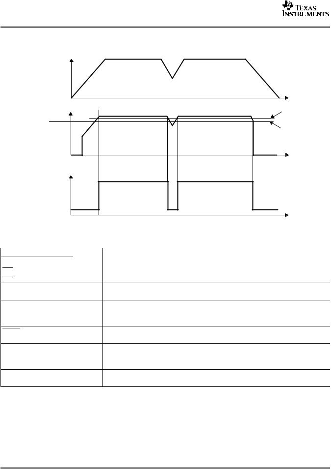
PG1 Timing Diagram
VIN1 |
|
VUVLO |
VUVLO |
|
|
VPG1 |
V |
|
PG |
(see Note A) |
|
|
t |
VOUT1 |
VIT+ |
Threshold |
(see Note B) |
|
|
Voltage |
|
VIT−
(see Note B)
|
|
t |
PG1 Output |
PG1 |
|
|
|
|
Output |
|
Output |
Undefined |
|
Undefined |
|
|
t |
NOTES A: VPG1 is the minimum input voltage for a valid PG. The symbol VPG1 is not currently listed within EIA or JEDEC |
||
standards for semiconductor symbology. |
|
|
B: VIT− trip voltage is typically 5% lower than the output voltage (95%VO). VIT− to VIT+ is the hysteresis voltage. |
||
Copyright © 2000–2007, Texas Instruments Incorporated |
Submit Documentation Feedback |
9 |
TPS70845, TPS70848
TPS70851, TPS70858
TPS70802
SLVS301D–JUNE 2000–REVISED DECEMBER 2007
PG2 Timing Diagram (assuming VIN1 already powered up)
VIN2
VOUT2
Threshold
Voltage
PG2
Output
www.ti.com
t
VIT+ (see Note A)
VIT−
(see Note A)
t
t
NOTE A: VIT− trip voltage is typically 5% lower than the output voltage (95%VO). VIT− to VIT+ is the hysteresis voltage.
|
|
|
TERMINAL FUNCTIONS |
|
TERMINAL |
I/O |
DESCRIPTION |
||
NAME |
NO. |
|||
|
|
|||
EN1 |
5 |
I |
Active low enable for VOUT1 |
|
EN2 |
6 |
I |
Active low enable for VOUT2 |
|
GND |
8 |
— |
Ground |
|
MR |
4 |
I |
Manual reset input, active low, pulled up internally |
|
NC |
1, 11, 20 |
— |
No connection |
|
PG1 |
16 |
O |
Open drain output, low when VOUT1 voltage is less than 95% of the nominal regulated voltage |
|
PG2 |
15 |
O |
Open drain output, low when VOUT2 voltage is less than 95% of the nominal regulated voltage |
|
RESET |
7 |
I |
Open drain output, SVS (power-on reset) signal, active low |
|
VIN1 |
2, 3 |
I |
Input voltage of regulator 1 |
|
VIN2 |
9, 10 |
I |
Input voltage of regulator 2 |
|
VOUT1 |
18, 19 |
O |
Output voltage of regulator 1 |
|
VOUT2 |
12, 13 |
O |
Output voltage of regulator 2 |
|
VSENSE2/FB2 |
14 |
I |
Regulator 2 output voltage sense/regulator 2 feedback for adjustable |
|
VSENSE1/FB1 |
17 |
I |
Regulator 1 output voltage sense/regulator 1 feedback for adjustable |
|
10 |
Submit Documentation Feedback |
Copyright © 2000–2007, Texas Instruments Incorporated |
TPS70845, TPS70848 TPS70851, TPS70858
TPS70802
www.ti.com
SLVS301D–JUNE 2000–REVISED DECEMBER 2007
Detailed Description
The TPS708xx low dropout regulator family provides dual regulated output voltages with independent enable functions. These devices provide fast transient response and high accuracy with small output capacitors, while drawing low quiescent current. Other features are integrated SVS (power-on reset, RESET) and power good (PG1, PG2) that monitor output voltages and provide logic output to the system. These differentiated features provide a complete power solution.
The TPS708xx, unlike many other LDOs, features very low quiescent current that remains virtually constant even with varying loads. Conventional LDO regulators use a PNP pass element, the base current of which is directly proportional to the load current through the regulator (IB = IC/β). The TPS708xx uses a PMOS transistor to pass current; because the gate of the PMOS is voltage-driven, operating current is low and stable over the full load range.
Pin Functions
Enable (EN1, EN2)
The EN terminals are inputs that enable or shut down each respective regulator. If EN is at a voltage high signal, the respective regulator is in shutdown mode. When EN goes to voltage low, the respective regulator is enabled.
Power-Good (PG1, PG2)
The PG terminals are open drain, active high output terminals that indicate the status of each respective
regulator. When VOUT1 reaches 95% of its regulated voltage, PG1 goes to a high impedance state. When VOUT2 reaches 95% of its regulated voltage, PG2 goes to a high impedance state. Each PG goes to a low impedance
state when its respective output voltage is pulled below 95% (that is, goes to an overload condition) of its regulated voltage. The open drain outputs of the PG terminals require a pull-up resistor.
Manual Reset Pin
MR is an active low input terminal used to trigger a reset condition. When MR is pulled to logic low, a POR (RESET) occurs. The terminal has a 6-μA pull-up current to VIN1.
Sense (VSENSE1, VSENSE2)
The sense terminals of fixed-output options must be connected to the regulator outputs, and the connection should be as short as possible. Internally, the sense terminal connects to high-impedance, wide-bandwidth amplifiers through a resistor-divider network and noise pickup feeds through to the regulator output. It is essential to route the sense connection in such a way as to minimize or avoid noise pickup. Adding RC networks between sense terminals and VOUT terminals to filter noise is not recommended because these networks can cause the regulators to oscillate.
Copyright © 2000–2007, Texas Instruments Incorporated |
Submit Documentation Feedback |
11 |

TPS70845, TPS70848
TPS70851, TPS70858
TPS70802
www.ti.com
SLVS301D–JUNE 2000–REVISED DECEMBER 2007
FB1 and FB2
FB1 and FB2 are input terminals used for adjustable-output devices and must be connected to the external feedback resistor divider. FB1 and FB2 connections should be as short as possible. It is essential to route them in such a way as to minimize or avoid noise pickup. Adding RC networks between FB terminals and VOUT terminals to filter noise is not recommended because these networks can cause the regulators to oscillate.
RESET Indicator
The TPS708xx features a RESET (SVS, POR, or power on reset). RESET can be used to drive power on reset circuitry or a low-battery indicator. RESET is an active low, open drain output that indicates the status of the manual reset pin (MR). When MR is in a high-impedance state, RESET goes to a high impedance state after a
120-ms delay. To monitor VOUT1, the PG1 output pin can be connected to MR. To monitor VOUT2, the PG2 output pin can be connected to MR. The open drain output of the RESET terminal requires a pull-up resistor. If RESET
is not used, it can be left floating.
VIN1 and VIN2
VIN1 and VIN2 are inputs to each regulator. Internal bias voltages are powered by VIN1.
VOUT1 and VOUT2
VOUT1 and VOUT2 are output terminals of each regulator.
12 |
Submit Documentation Feedback |
Copyright © 2000–2007, Texas Instruments Incorporated |
Loading...