


TPA1517NEEVM
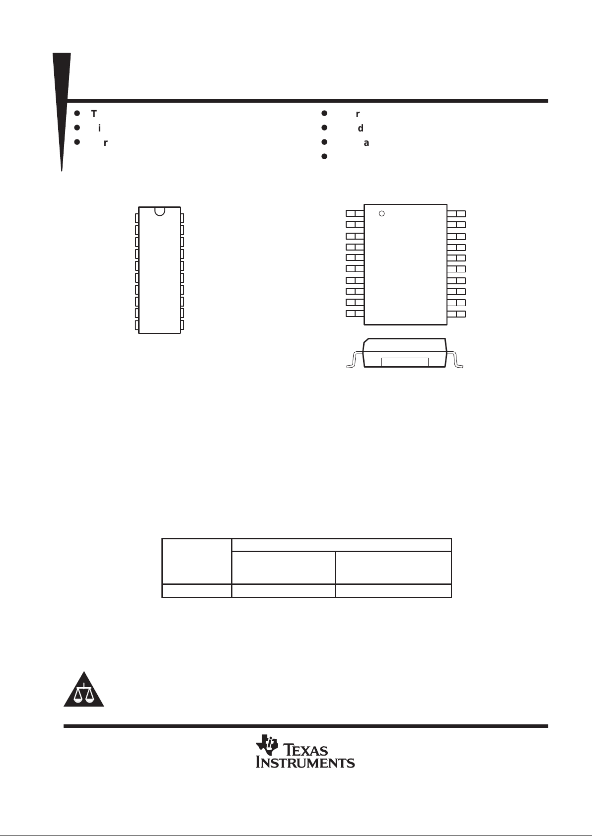
TPA1517
6-W STEREO AUDIO POWER AMPLIFIER
SLOS162B – MARCH 1997 – REVISED MARCH 2000
1
POST OFFICE BOX 655303 • DALLAS, TEXAS 75265
D
TDA1517P Compatible
D
High Power Outputs (6 W/Channel)
D
Surface Mount Availability
20-Pin Thermal SOIC PowerP AD
D
Thermal Protection
D
Fixed Gain . . . 20 dB
D
Mute and Standby Operation
D
Supply Range . . . 9.5 V – 18 V
1
2
3
4
5
6
7
8
9
10
20
19
18
17
16
15
14
13
12
11
IN1
SGND
SVRR
OUT1
PGND
OUT2
V
CC
M/SB
IN2
GND/HS
GND/HS
GND/HS
GND/HS
GND/HS
GND/HS
GND/HS
GND/HS
GND/HS
GND/HS
GND/HS
NE PACKAGE
(TOP VIEW)
1
2
3
4
5
6
7
8
9
10
20
19
18
17
16
15
14
13
12
11
GND/HS
IN1
NC
SGND
SVRR
NC
OUT1
OUT1
PGND
GND/HS
GND/HS
IN2
NC
M/SB
V
CC
NC
OUT2
OUT2
PGND
GND/HS
DWP PACKAGE
(TOP VIEW)
Cross Section View Showing PowerPAD
NC – No internal connection
description
The TP A1517 is a stereo audio power amplifier that contains two identical amplifiers capable of delivering 6 W
per channel of continuous average power into a 4-Ω load at 10% THD+N or 5 W per channel at 1% THD+N.
The gain of each channel is fixed at 20 dB. The amplifier features a mute/standby function for power-sensitive
applications. The amplifier is available in Texas Instruments patented PowerPAD 20-pin surface-mount
thermally-enhanced package (DWP) that reduces board space and facilitates automated assembly while
maintaining exceptional thermal characteristics. It is also available in the 20-pin thermally enhanced DIP
package (NE).
AVAILABLE OPTIONS
PACKAGED DEVICES
T
A
THERMALLY ENHANCED
PLASTIC DIP
THERMALLY† ENHANCED
SURFACE MOUNT
(DWP)
–40°C to 85°C TPA1517NE TPA1517DWP
†
The DWP package is available taped and reeled. To order a taped and reeled part,
add the suffix R (e.g., TPA1517DWPR).
PRODUCTION DATA information is current as of publication date.
Products conform to specifications per the terms of Texas Instruments
standard warranty. Production processing does not necessarily include
testing of all parameters.
Copyright 2000, Texas Instruments Incorporated
Please be aware that an important notice concerning availability, standard warranty, and use in critical applications of
Texas Instruments semiconductor products and disclaimers thereto appears at the end of this data sheet.
PowerPAD is a trademark of Texas Instruments Incorporated.
TPA1517
6-W STEREO AUDIO POWER AMPLIFIER
SLOS162B – MARCH 1997 – REVISED MARCH 2000
2
POST OFFICE BOX 655303 • DALLAS, TEXAS 75265
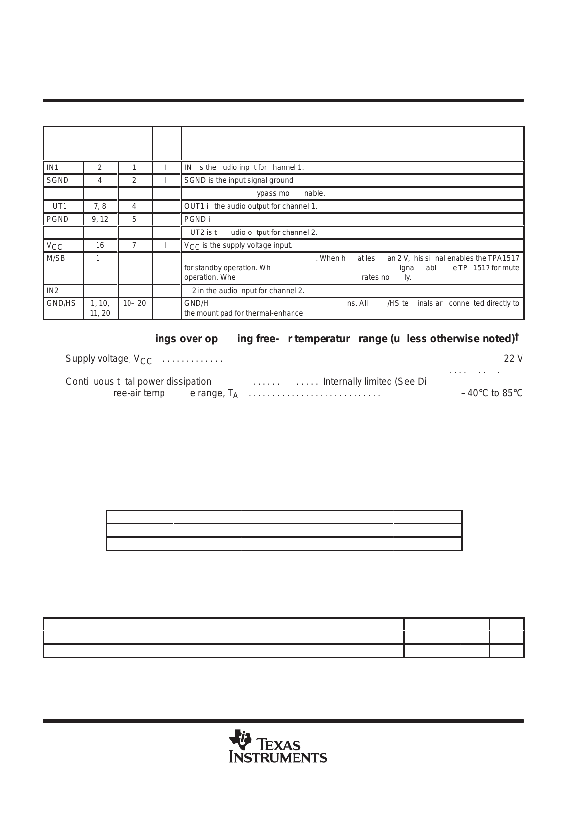
Terminal Functions
TERMINAL
NAME DWP
NO.
NE
NO.
I/O
DESCRIPTION
IN1
2
1
I
IN1 is the audio input for channel 1.
SGND
4
2
I
SGND is the input signal ground reference.
SVRR
5
3
SVRR is the midrail bypass mode enable.
OUT1
7, 8
4
O
OUT1 is the audio output for channel 1.
PGND
9, 12
5
PGND is the power ground reference.
OUT2
13, 14
6
O
OUT2 is the audio output for channel 2.
V
CC
16
7
I
VCC is the supply voltage input.
ÁÁ
Á
M/SB
Á
Á
17
ÁÁ
Á
8
Á
Á
I
ББББББББББББББББББББББ
Á
M/SB is the mute/standby mode enable. When held at less than 2 V , this signal enables the TP A1517
for standby operation. When held between 3.4 V and 8.8 V , this signal enables the TP A1517 for mute
operation. When held above 9.2 V, the TPA1517 operates normally.
IN2
19
9
I
IN2 in the audio input for channel 2.
ÁÁ
Á
GND/HS
Á
Á
1, 10,
11, 20
ÁÁ
Á
10– 20
ÁÁББББББББББББББББББББББ
Á
GND/HS are the ground and heatsink connections. All GND/HS terminals are connected directly to
the mount pad for thermal-enhanced operation.
absolute maximum ratings over operating free-air temperature range (unless otherwise noted)
†
Supply voltage, VCC 22 V. . . . . . . . . . . . . . . . . . . . . . . . . . . . . . . . . . . . . . . . . . . . . . . . . . . . . . . . . . . . . . . . . . . . . . .
Input voltage, VI (IN1, IN2) 22 V. . . . . . . . . . . . . . . . . . . . . . . . . . . . . . . . . . . . . . . . . . . . . . . . . . . . . . . . . . . . . . . . . .
Continuous total power dissipation Internally limited (See Dissipation Rating Table). . . . . . . . . . . . . . . . . . . . .
Operating free-air temperature range, TA –40°C to 85°C. . . . . . . . . . . . . . . . . . . . . . . . . . . . . . . . . . . . . . . . . . . .
Operating junction temperature range, TJ –40°C to 150°C. . . . . . . . . . . . . . . . . . . . . . . . . . . . . . . . . . . . . . . . . . .
Storage temperature range, T
stg
–65°C to 150°C. . . . . . . . . . . . . . . . . . . . . . . . . . . . . . . . . . . . . . . . . . . . . . . . . . .
Lead temperature 1,6 mm (1/16 inch) from case for 10 seconds: DWP or NE package 260°C. . . . . . . . . . . .
†
Stresses beyond those listed under “absolute maximum ratings” may cause permanent damage to the device. These are stress ratings only, and
functional operation of the device at these or any other conditions beyond those indicated under “recommended operating conditions” is not
implied. Exposure to absolute-maximum-rated conditions for extended periods may affect device reliability.
NOTE 1: These devices have been classified as Class 1 ESD sensitive products per MIL-PRF-38535 Method 3015.7. Appropriate precautions
should be taken to prevent serious damage to the device.
DISSIPATION RATING TABLE
PACKAGE
TA ≤ 25°C
DERATING FACTOR TA = 70°C TA = 85°C
DWP
‡
2.94 W
23.5 mW/°C
1.88 W
1.53 W
NE
‡
2.85 W
22.8 mW/°C 1.82 W 1.48 W
‡
See the Texas Instruments document,
PowerPAD Thermally Enhanced Package Application Report
(literature number SLMA002), for more information on the PowerPAD package. The thermal data was
measured on a PCB layout based on the information in the section entitled
Texas Instruments
Recommended Board for PowerPAD
on page 33 of the before mentioned document.
recommended operating conditions
MIN NOM MAX UNIT
Supply voltage, V
CC
9.5
18
V
Operating free-air temperature, T
A
–40
85
°C
TPA1517
6-W STEREO AUDIO POWER AMPLIFIER
SLOS162B – MARCH 1997 – REVISED MARCH 2000
3
POST OFFICE BOX 655303 • DALLAS, TEXAS 75265
electrical characteristics, VCC = 12 V, TA = 25°C (unless otherwise noted)
PARAMETER TEST CONDITIONS
MIN TYP MAX UNIT
I
CC
БББББББББББББББББ
Supply current
45
70
mA
V
O(DC)
DC output voltage See Note 2 4 V
V
(M/SB)
M/SB on voltage 9.5 V
V
O(M)
Mute output voltage VI = 1 V (max) 2 mV
I
CC(SB)
Supply current in standby mode 7 100 µA
NOTE 2: At 6 V < VCC < 18 V the DC output voltage is approximately VCC/2.
electrical characteristics, VCC = 14.5 V, TA = 25°C (unless otherwise noted)
PARAMETER TEST CONDITIONS
MIN TYP MAX UNIT
I
CC
БББББББББББББББББ
Supply current
50
80
mA
V
O(DC)
DC output voltage See Note 2 5 V
V
(M/SB)
Voltage on M/SB terminal for normal operation 9.5 V
V
O(M)
Mute output voltage VI = 1 V (max) 2 mV
I
CC(SB)
Supply current in standby mode 7 100 µA
NOTE 2: At 6 V < VCC < 18 V the DC output voltage is approximately VCC/2.
operating characteristic, V
CC
= 12 V, R
L
= 4 Ω, f = 1 kHz, TA = 25°C
PARAMETER TEST CONDITIONS
MIN TYP MAX UNIT
p
p
THD = 0.2%
3
POOutput power (see Note 3)
THD = 10%
6
W
SNR Signal-to-noise ratio 84 dB
THD Total harmonic distortion PO = 1 W, RL = 8 Ω, f = 1 kHz 0.1%
I
O(SM)
Non-repetitive peak output current
4
A
I
O(RM)
Repetitive peak output current
2.5
A
Low-frequency roll-off
–3 dB
45
Hz
High-frequency roll-off
–1 dB
20
kHz
Supply ripple rejection ratio
M/SB = On, f = 1 kHz
65
dB
Z
I
Input impedance
60
kΩ
Rs = 0,
M/SB = On
50
µV(rms)
V
n
Noise output voltage (see Note 4)
Rs = 10 kΩ,
M/SB = On
70
µV(rms)
M/SB = Mute
50
µV(rms)
Channel separation
Rs = 10 kΩ
58
dB
Gain 18.5 20 21
Channel balance
0.1
1
dB
NOTES: 3. Output power is measured at the output terminals of the IC.
4. Noise voltage is measured in a bandwidth of 20 Hz to 20 kHz.
TPA1517
6-W STEREO AUDIO POWER AMPLIFIER
SLOS162B – MARCH 1997 – REVISED MARCH 2000
4
POST OFFICE BOX 655303 • DALLAS, TEXAS 75265
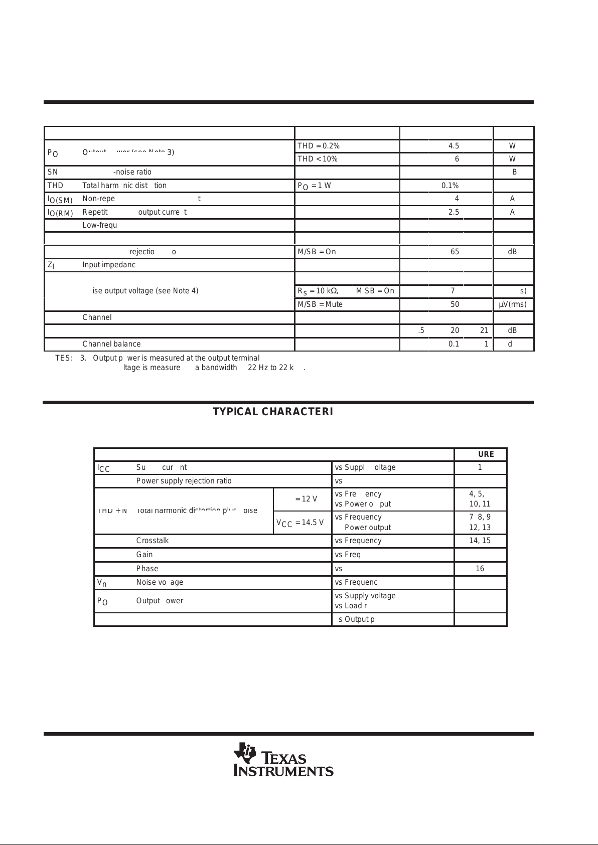
operating characteristic, V
CC
= 14.5 V, RL = 4 Ω, f = 1 kHz, TA = 25°C
PARAMETER TEST CONDITIONS
MIN TYP MAX UNIT
p
p
THD = 0.2%
4.5
W
POOutput power (see Note 3)
THD < 10%
6
W
SNR Signal-to-noise ratio 84 dB
THD Total harmonic distortion PO = 1 W 0.1%
I
O(SM)
Non-repetitive peak output current
4
A
I
O(RM)
Repetitive peak output current
2.5
A
Low-frequency roll-off
–3 dB
45
Hz
High-frequency roll-off
–1 dB
20
kHz
Supply ripple rejection ratio
M/SB = On
65
dB
Z
I
Input impedance
60
kΩ
Rs = 0,
M/SB = On
50
µV(rms)
V
n
Noise output voltage (see Note 4)
Rs = 10 kΩ,
M/SB = On
70
µV(rms)
M/SB = Mute
50
µV(rms)
Channel separation
Rs = 10 kΩ
58
dB
Gain 18.5 20 21 dB
Channel balance
0.1
1
dB
NOTES: 3. Output power is measured at the output terminals of the IC.
4. Noise voltage is measured in a bandwidth of 22 Hz to 22 kHz.
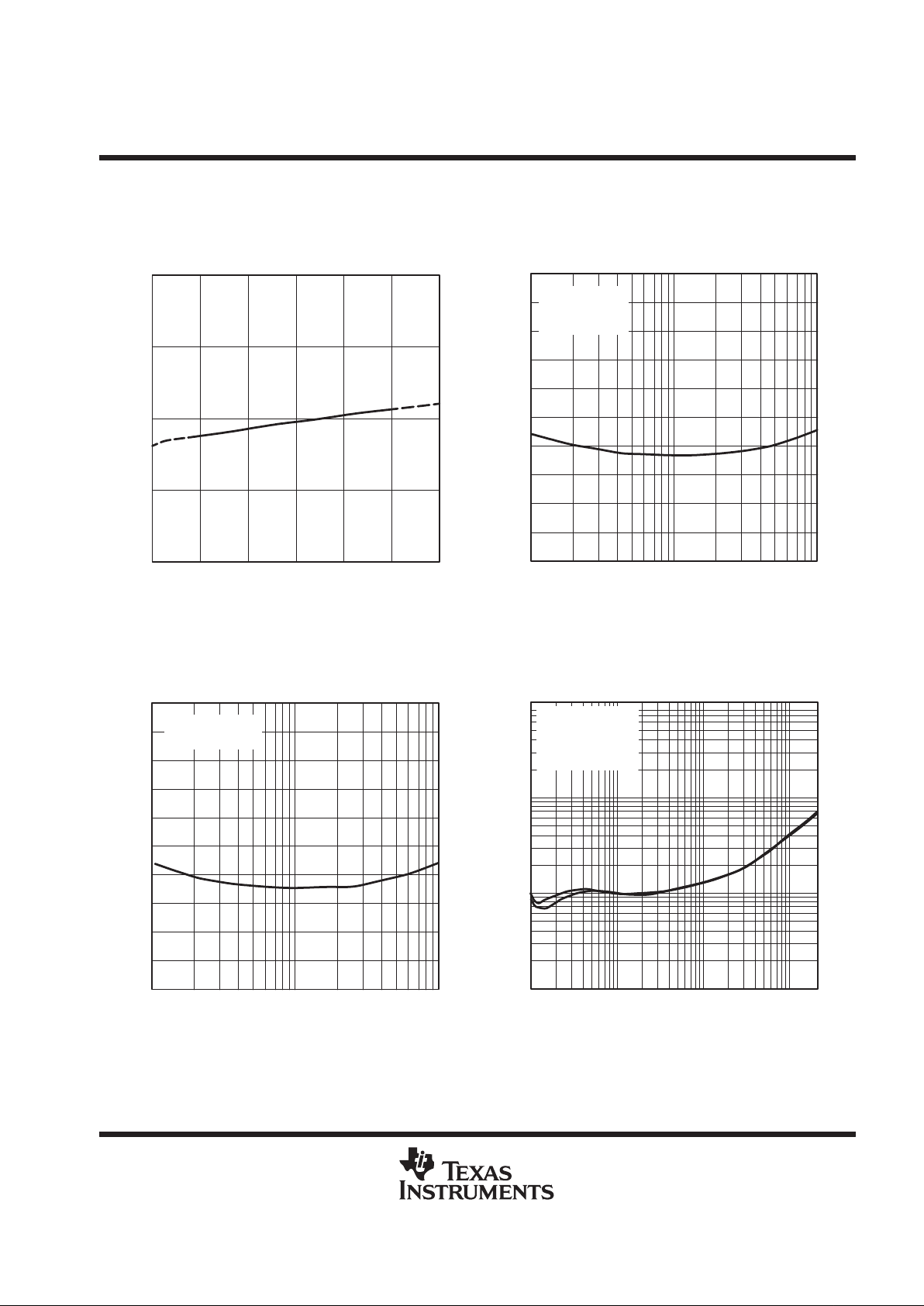
TYPICAL CHARACTERISTICS
Table of Graphs
FIGURE
I
CC
Supply current vs Supply voltage 1
Power supply rejection ratio vs Frequency 2, 3
p
VCC = 12 V
vs Frequency
vs Power output
4, 5, 6
10, 11
THD
+
N
Total harmonic distortion plus noise
VCC = 14.5 V
vs Frequency
vs Power output
7, 8, 9
12, 13
Crosstalk vs Frequency 14, 15
Gain vs Frequency 16
Phase vs Frequency 16
V
n
Noise voltage vs Frequency 17, 18
P
O
Output power
vs Supply voltage
vs Load resistance
19
20
P
D
Power dissipation vs Output power 21, 22
TPA1517
6-W STEREO AUDIO POWER AMPLIFIER
SLOS162B – MARCH 1997 – REVISED MARCH 2000
5
POST OFFICE BOX 655303 • DALLAS, TEXAS 75265
TYPICAL CHARACTERISTICS
Figure 1
50
0
81012
– Supply Current – mA
SUPPLY CURRENT
vs
SUPPLY VOLTAGE
100
14 16 18 20
I
CC
VCC – Supply Voltage – V
25
75
Figure 2
– 50
– 60
– 80
– 90
– 100
0
– 70
100 1 k 10 k
Supply Ripple Rejection Ratio – dB
– 30
– 40
– 20
f – Frequency – Hz
SUPPLY RIPPLE REJECTION RATIO
vs
FREQUENCY
– 10
VCC = 12 V
RL = 4 Ω
CB = 100 µF
Figure 3
– 50
– 60
– 80
– 100
100 1 k
– 30
– 10
SUPPLY RIPPLE REJECTION RATIO
vs
FREQUENCY
0
10 K
– 20
– 40
– 70
– 90
VCC = 14.5 V
RL = 4 Ω
f – Frequency – Hz
Supply Ripple Rejection Ratio – dB
Figure 4
0.1%
0.01%
20 100
THD+N – Total Harmonic Distortion + Noise
1%
f – Frequency – Hz
TOTAL HARMONIC DISTORTION PLUS NOISE
vs
FREQUENCY
10%
1 k 10 k 20 k
VCC = 12 V
RL = 4 Ω
PO = 3 W
Both Channels
TPA1517
6-W STEREO AUDIO POWER AMPLIFIER
SLOS162B – MARCH 1997 – REVISED MARCH 2000
6
POST OFFICE BOX 655303 • DALLAS, TEXAS 75265
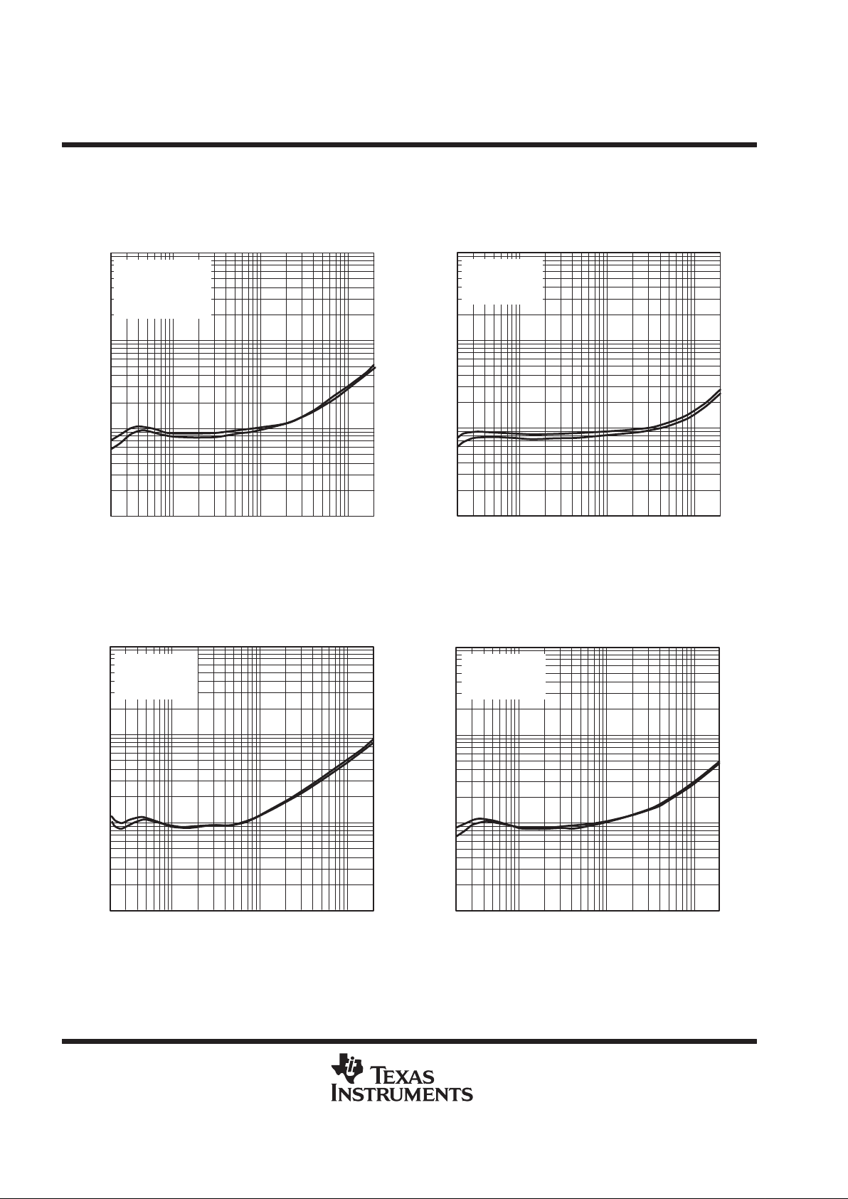
TYPICAL CHARACTERISTICS
Figure 5
0.1%
0.01%
20 100 1 k
THD+N – Total Harmonic Distortion + Noise
1%
f – Frequency – Hz
TOTAL HARMONIC DISTORTION PLUS NOISE
vs
FREQUENCY
10%
10 k 20 k
VCC = 12 V
RL = 8 Ω
PO = 1 W
Both Channels
Figure 6
20
0.1%
0.01%
100 1 k
THD+N – Total Harmonic Distortion + Noise
1%
f – Frequency – Hz
TOTAL HARMONIC DISTORTION PLUS NOISE
vs
FREQUENCY
10%
10 k 20 k
VCC = 12 V
RL = 32 Ω
PO = 0.25 W
Figure 7
20
0.1%
0.01%
100 1 k
THD+N – Total Harmonic Distortion + Noise
1%
f – Frequency – Hz
TOTAL HARMONIC DISTORTION PLUS NOISE
vs
FREQUENCY
10%
10 k 20 k
VCC = 14.5 V
RL = 4 Ω
PO = 3 W
Figure 8
20
0.1%
0.01%
100 1 k
THD+N – Total Harmonic Distortion + Noise
1%
f – Frequency – Hz
TOTAL HARMONIC DISTORTION PLUS NOISE
vs
FREQUENCY
10%
10 k 20 k
VCC = 14.5 V
RL = 8 Ω
PO = 1.5 W
 Loading...