


 Loading...
TMS320F28335, TMS320F28334, TMS320F28332
Digital Signal Controllers (DSCs)
Data Manual
Literature Number: SPRS439
June 2007
PRODUCT PREVIEW information concerns products in the formative or design phase of development. Characteristic data and other specifications are design goals. Texas Instruments reserves the right to change or discontinue these products without notice.

TMS320F28335, TMS320F28334, TMS320F28332
Digital Signal Controllers (DSCs)
www.ti.com
SPRS439 –JUNE 2007
Contents
1 |
TMS320F28335, TMS320F28334, TMS320F28332 DSCs ............................................................. |
7 |
||
|
1.1 |
Features |
....................................................................................................................... |
7 |
|
1.2 |
Getting Started ............................................................................................................... |
8 |
|
2 |
Introduction......................................................................................................................... |
|
9 |
|
|
2.1 |
Pin Assignments ............................................................................................................. |
9 |
|
|
2.2 |
Signal Descriptions......................................................................................................... |
15 |
|
3 |
Functional Overview ........................................................................................................... |
24 |
||
|
3.1 |
Memory Maps .............................................................................................................. |
25 |
|
|
3.2 |
Brief Descriptions........................................................................................................... |
32 |
|
|
|
3.2.1 ....................................................................................................... |
C28x CPU |
32 |
|
|
3.2.2 .................................................................... |
Memory Bus (Harvard Bus Architecture) |
32 |
|
|
3.2.3 .................................................................................................. |
Peripheral Bus |
32 |
|
|
3.2.4 ................................................................................ |
Real - Time JTAG and Analysis |
32 |
|
|
3.2.5 ..................................................................................... |
External Interface (XINTF) |
33 |
|
|
3.2.6 .............................................................................................................. |
Flash |
33 |
|
|
3.2.7 ............................................................................................... |
M0, M1 SARAMs |
33 |
|
|
3.2.8 ..................................................................... |
L0, L1, L2, L3, L4, L5, L6, L7 SARAMs |
33 |
|
|
3.2.9 ........................................................................................................ |
Boot ROM |
33 |
|
|
3.2.10 .......................................................................................................... |
Security |
35 |
|
|
3.2.11 .................................................................. |
Peripheral Interrupt Expansion (PIE) Block |
35 |
|
|
3.2.12 .................................................................... |
External Interrupts (XINT1 - XINT7, XNMI) |
36 |
|
|
3.2.13 .............................................................................................. |
Oscillator and PLL |
36 |
|
|
3.2.14 ........................................................................................................ |
Watchdog |
36 |
|
|
3.2.15 ............................................................................................. |
Peripheral Clocking |
36 |
|
|
3.2.16 .............................................................................................. |
Low - Power Modes |
36 |
|
|
3.2.17 ........................................................................... |
Peripheral Frames 0, 1, 2, 3 (PFn) |
37 |
|
|
3.2.18 ......................................................... |
General - Purpose Input/Output (GPIO) Multiplexer |
37 |
|
|
3.2.19 ................................................................................... |
32 - Bit CPU - Timers (0, 1, 2) |
37 |
|
|
3.2.20 ............................................................................................. |
Control Peripherals |
38 |
|
|
3.2.21 ......................................................................................... |
Serial Port Peripherals |
38 |
|
3.3 |
Register ................................................................................................................Map |
39 |
|
|
3.4 |
Device Emulation ...............................................................................................Registers |
40 |
|
|
3.5 |
Interrupts .................................................................................................................... |
41 |
|
|
|
3.5.1 .............................................................................................. |
External Interrupts |
45 |
|
3.6 |
System Control ............................................................................................................. |
45 |
|
|
|
3.6.1 ............................................................................................ |
OSC and PLL Block |
47 |
|
|
3.6.2 ................................................................................................. |
Watchdog Block |
50 |
|
3.7 |
Low-Power ..................................................................................................Modes Block |
51 |
|
4 |
Peripherals ........................................................................................................................ |
|
52 |
|
|
4.1 |
DMA Overview.............................................................................................................. |
53 |
|
|
4.2 |
32-Bit CPU ..................................................................................................-Timers 0/1/2 |
54 |
|
|
4.3 |
Enhanced ..........................................................................PWM Modules (ePWM1/2/3/4/5/6) |
56 |
|
|
4.4 |
High-Resolution ........................................................................................PWM (HRPWM) |
58 |
|
|
4.5 |
Enhanced ............................................................................CAP Modules (eCAP1/2/3/4/5/6) |
59 |
|
|
4.6 |
Enhanced .....................................................................................QEP Modules (eQEP1/2) |
61 |
|
|
4.7 |
Enhanced ................................................................Analog-to-Digital Converter (ADC) Module |
63 |
|
|
|
4.7.1 ................................................................... |
ADC Connections if the ADC Is Not Used |
66 |
|
|
4.7.2 ................................................................................................... |
ADC Registers |
66 |
|
4.8 |
Multichannel ...................................................................Buffered Serial Port (McBSP) Module |
68 |
|
|
4.9 |
Enhanced .....................................Controller Area Network (eCAN) Modules (eCAN-A and eCAN-B) |
71 |
|
2 |
Contents |
Submit Documentation Feedback |

TMS320F28335, TMS320F28334, TMS320F28332
Digital Signal Controllers (DSCs)
www.ti.com
|
|
|
SPRS439 – JUNE 2007 |
|
4.10 |
Serial Communications Interface (SCI) Modules (SCI-A, SCI-B, SCI-C) |
........................................... 76 |
|
4.11 |
Serial Peripheral Interface (SPI) Module (SPI-A) ...................................................................... |
80 |
|
4.12 |
Inter-Integrated Circuit (I2C) .............................................................................................. |
83 |
|
4.13 |
GPIO MUX .................................................................................................................. |
85 |
5 |
Device Support .................................................................................................................. |
91 |
|
|
5.1 |
Device and Development Support Tool Nomenclature................................................................ |
91 |
|
5.2 |
Documentation Support ................................................................................................... |
93 |
6 |
Electrical Specifications ...................................................................................................... |
96 |
|
|
6.1 |
Absolute Maximum Ratings ............................................................................................... |
96 |
|
6.2 |
Recommended Operating Conditions ................................................................................... |
97 |
|
6.3 |
Electrical Characteristics ................................................................................................. |
97 |
Contents 3

TMS320F28335, TMS320F28334, TMS320F28332
Digital Signal Controllers (DSCs)
www.ti.com
SPRS439 –JUNE 2007
List of Figures
2-1 |
F28335, F28334, F28332 176-Pin PGF LQFP (Top View) |
.................................................................. |
10 |
2-2 |
F28335, F28334, F28332 179-Ball ZHH MicroStar BGA™ |
(Upper Left Quadrant) (Bottom View) .................... |
11 |
2-3 |
F28335, F28334, F28332 179-Ball ZHH MicroStar BGA™ |
(Upper Right Quadrant) (Bottom View) .................. |
12 |
2-4 |
F28335, F28334, F28332 179-Ball ZHH MicroStar BGA™ .................... |
(Lower Left Quadrant) (Bottom View) |
13 |
2-5 |
F28335, F28334, F28332 179-Ball ZHH MicroStar BGA™ .................. |
(Lower Right Quadrant) (Bottom View) |
14 |
3-1 |
Functional Block Diagram ....................................................................................................... |
|
24 |
3-2 |
F28335 Memory Map ............................................................................................................. |
|
26 |
3-3 |
F28334 Memory Map ............................................................................................................. |
|
27 |
3-4 |
F28332 Memory Map ............................................................................................................. |
|
28 |
3-5 |
External and PIE Interrupt Sources............................................................................................. |
|
41 |
3-6 |
External Interrupts ................................................................................................................ |
|
42 |
3-7 |
Multiplexing of Interrupts Using the PIE Block ................................................................................ |
|
43 |
3-8 |
Clock and Reset Domains ....................................................................................................... |
|
46 |
3-9 |
OSC and PLL Block Diagram ................................................................................................... |
|
47 |
3-10 |
Using a 3.3-V External Oscillator ............................................................................................... |
|
48 |
3-11 |
Using a 1.8-V External Oscillator ............................................................................................... |
|
48 |
3-12 |
Using the Internal Oscillator ..................................................................................................... |
|
48 |
3-13 |
Watchdog Module................................................................................................................. |
|
50 |
4-1 |
DMA Functional Block Diagram ................................................................................................. |
|
53 |
4-2 |
CPU-Timers........................................................................................................................ |
|
54 |
4-3 |
CPU-Timer Interrupt Signals and Output Signal .............................................................................. |
|
54 |
4-4 |
Multiple PWM Modules in a 2833x System.................................................................................... |
|
56 |
4-5 |
ePWM Sub-Modules Showing Critical Internal Signal Interconnections ................................................... |
58 |
|
4-6 |
eCAP Functional Block Diagram ................................................................................................ |
|
59 |
4-7 |
eQEP Functional Block Diagram................................................................................................ |
|
61 |
4-8 |
Block Diagram of the ADC Module ............................................................................................. |
|
64 |
4-9 |
ADC Pin Connections With Internal Reference ............................................................................... |
|
65 |
4-10 |
ADC Pin Connections With External Reference .............................................................................. |
|
65 |
4-11 |
McBSP Module ................................................................................................................... |
|
69 |
4-12 |
eCAN Block Diagram and Interface Circuit .................................................................................... |
|
72 |
4-13 |
eCAN-A Memory Map ............................................................................................................ |
|
73 |
4-14 |
eCAN-B Memory Map ............................................................................................................ |
|
74 |
4-15 |
Serial Communications Interface (SCI) Module Block Diagram ............................................................ |
79 |
|
4-16 |
SPI Module Block Diagram (Slave Mode) ..................................................................................... |
|
82 |
4-17 |
I2C Peripheral Module Interfaces ............................................................................................... |
|
84 |
4-18 |
GPIO MUX Block Diagram....................................................................................................... |
|
85 |
4-19 |
Qualification Using Sampling Window.......................................................................................... |
|
90 |
5-1 |
Example of 2833x Device Nomenclature ...................................................................................... |
|
92 |
4 |
List of Figures |
Submit Documentation Feedback |

|
TMS320F28335, TMS320F28334, TMS320F28332 |
|
|
www.ti.com |
Digital Signal Controllers (DSCs) |
|
SPRS439 –JUNE 2007 |
|
|
|
|
|
List of Tables |
|
2-1 |
Hardware Features ................................................................................................................ |
9 |
2-2 |
Signal Descriptions ............................................................................................................... |
15 |
3-1 |
Addresses of Flash Sectors in F28335......................................................................................... |
29 |
3-2 |
Addresses of Flash Sectors in F28334......................................................................................... |
29 |
3-3 |
Addresses of Flash Sectors in F28332......................................................................................... |
29 |
3-4 |
Handling Security Code Locations.............................................................................................. |
30 |
3-5 |
Wait-states ......................................................................................................................... |
31 |
3-6 |
Boot Mode Selection.............................................................................................................. |
34 |
3-7 |
Peripheral Frame 0 Registers ................................................................................................... |
39 |
3-8 |
Peripheral Frame 1 Registers ................................................................................................... |
39 |
3-9 |
Peripheral Frame 2 Registers ................................................................................................... |
40 |
3-10 |
Peripheral Frame 3 Registers ................................................................................................... |
40 |
3-11 |
Device Emulation Registers ..................................................................................................... |
40 |
3-12 |
PIE Peripheral Interrupts ......................................................................................................... |
43 |
3-13 |
PIE Configuration and Control Registers ...................................................................................... |
44 |
3-14 |
External Interrupt Registers...................................................................................................... |
45 |
3-15 |
PLL, Clocking, Watchdog, and Low-Power Mode Registers ................................................................ |
47 |
3-16 |
PLLCR Register Bit Definitions.................................................................................................. |
49 |
3-17 |
CLKIN Divide Options ............................................................................................................ |
49 |
3-18 |
Possible PLL Configuration Modes ............................................................................................. |
49 |
3-19 |
Low-Power Modes ................................................................................................................ |
51 |
4-1 |
CPU-Timers 0, 1, 2 Configuration and Control Registers ................................................................... |
55 |
4-2 |
ePWM Control and Status Registers ........................................................................................... |
57 |
4-3 |
eCAP Control and Status Registers ............................................................................................ |
60 |
4-4 |
eQEP Control and Status Registers ............................................................................................ |
62 |
4-5 |
ADC Registers..................................................................................................................... |
66 |
4-6 |
McBSP Register Summary ...................................................................................................... |
70 |
4-7 |
3.3-V eCAN Transceivers ....................................................................................................... |
72 |
4-8 |
CAN Register Map ................................................................................................................ |
75 |
4-9 |
SCI-A Registers ................................................................................................................... |
77 |
4-10 |
SCI-B Registers ................................................................................................................... |
77 |
4-11 |
SCI-C Registers ................................................................................................................... |
78 |
4-12 |
SPI-A Registers ................................................................................................................... |
81 |
4-13 |
I2C-A Registers.................................................................................................................... |
84 |
4-14 |
GPIO Registers ................................................................................................................... |
86 |
4-15 |
GPIO-A Mux Peripheral Selection Matrix ..................................................................................... |
87 |
4-16 |
GPIO-B Mux Peripheral Selection Matrix ..................................................................................... |
88 |
4-17 |
GPIO-C Mux Peripheral Selection Matrix ..................................................................................... |
89 |
List of Tables |
5 |

TMS320F28335, TMS320F28334, TMS320F28332
Digital Signal Controllers (DSCs)
www.ti.com
SPRS439 –JUNE 2007
6 |
List of Tables |
Submit Documentation Feedback |
TMS320F28335, TMS320F28334, TMS320F28332
Digital Signal Controllers (DSCs)
www.ti.com
SPRS439 –JUNE 2007
1 TMS320F28335, TMS320F28334, TMS320F28332 DSCs
1.1Features
∙High-Performance Static CMOS Technology
–Up to 150 MHz (6.67-ns Cycle Time)
–1.9-V Core, 3.3-V I/O Design
∙High-Performance 32-Bit CPU (TMS320C28x)
–IEEE-754 Single-Precision Floating-Point Unit (FPU)
–16 x 16 and 32 x 32 MAC Operations
–16 x 16 Dual MAC
–Harvard Bus Architecture
–Fast Interrupt Response and Processing
–Unified Memory Programming Model
–Code-Efficient (in C/C++ and Assembly)
∙Six Channel DMA Controller (for ADC, McBSP, XINTF, and SARAM)
∙16-bit or 32-bit External Memory Interface (XINTF)
∙On-Chip Memory
–F28335: 256K x 16 Flash, 34K x 16 SARAM
–F28334:128K x 16 Flash, 34K x 16 SARAM
–F28332: 64K x 16 Flash, 26K x 16 SARAM
–1K x 16 OTP ROM
∙Boot ROM (8K x 16)
–With Software Boot Modes (via SCI, SPI, CAN, I2C, McBSP, XINTF, and Parallel I/O)
–Standard Math Tables
∙Clock and System Control
–Dynamic PLL Ratio Changes Supported
–On-Chip Oscillator
–Watchdog Timer Module
∙Any GPIO Pin Can Be Connected to One of the Eight External Core Interrupts
∙Peripheral Interrupt Expansion (PIE) Block That Supports All 58 Peripheral Interrupts
∙128-Bit Security Key/Lock
–Protects Flash/OTP/RAM Blocks
–Prevents Firmware Reverse Engineering
∙Three 32-Bit CPU Timers
∙Enhanced Control Peripherals
–Up to 18 PWM Outputs
–Up to 6 HRPWM Outputs With 150 ps MEP Resolution
–Up to 6 Event Capture Inputs
–Up to 2 Quadrature Encoder Interfaces
–Up to 6 32-bit/Six 16-bit Timers
∙Serial Port Peripherals
–Up to 2 CAN Modules
–Up to 3 SCI (UART) Modules
–Up to 2 McBSP/SPI Modules
–Dedicated SPI Module
–One Inter-Integrated-Circuit (I2C) Bus
∙12-Bit ADC, 16 Channels
–80-ns Conversion Rate
–2 x 8 Channel Input Multiplexer
–Two Sample-and-Hold
–Single/Simultaneous Conversions
–Internal or External Reference
∙Up to 88 Individually Programmable, Multiplexed GPIO Pins With Input Filtering
∙JTAG Boundary Scan Support(1)
∙Advanced Emulation Features
–Analysis and Breakpoint Functions
–Real-Time Debug via Hardware
∙Development Support Includes
–ANSI C/C++ Compiler/Assembler/Linker
–Code Composer Studio™ IDE
–DSP/BIOS™
–Digital Motor Control and Digital Power Software Libraries
∙Low-Power Modes and Power Savings
–IDLE, STANDBY, HALT Modes Supported
–Disable Individual Peripheral Clocks
∙Package Options
–Lead-free Green Packaging
–Thin Quad Flatpack (PGF)
– MicroStar BGA™ (ZHH)
∙Temperature Options:
–A: -40°C to 85°C
–S: -40°C to 125°C
(1)IEEE Standard 1149.1-1990 Standard Test Access Port and Boundary Scan Architecture
Please be aware that an important notice concerning availability, standard warranty, and use in critical applications of Texas Instruments semiconductor products and disclaimers thereto appears at the end of this document.
Code Composer Studio, DSP/BIOS, MicroStar BGA, TMS320C28x, C28x, TMS320C2000, TMS320C54x, TMS320C55x are trademarks of Texas Instruments.
PRODUCT PREVIEW information concerns products in the |
Copyright © 2007, Texas Instruments Incorporated |
formative or design phase of development. Characteristic data and |
|
other specifications are design goals. Texas Instruments reserves |
|
the right to change or discontinue these products without notice. |
|
PRODUCT PREVIEW

TMS320F28335, TMS320F28334, TMS320F28332
Digital Signal Controllers (DSCs)
www.ti.com
SPRS439 –JUNE 2007
1.2Getting Started
This section gives a brief overview of the steps to take when first developing for a C28x device. For more detail on each of these steps, see the following:
∙ Getting Started With TMS320C28x™ Digital Signal Controllers (literature number SPRAAM0).
∙C2000 Getting Started Website (http://www.ti.com/c2000getstarted)
PREVIEW PRODUCT
8 |
TMS320F28335, TMS320F28334, TMS320F28332 DSCs |
Submit Documentation Feedback |

TMS320F28335, TMS320F28334, TMS320F28332
Digital Signal Controllers (DSCs)
www.ti.com
SPRS439 –JUNE 2007
2 Introduction
The TMS320F28335, TMS320F28334, and TMS320F28332, devices, members of the TMS320C28x™ DSC generation, are highly integrated, high-performance solutions for demanding control applications.
Throughout this document, TMS320F28335, TMS320F28334, and TMS320F28332, are abbreviated as F28335, F28334, and F28332, respectively. Table 2-1 provides a summary of features for each device.
Table 2-1. Hardware Features
FEATURE |
F28335 (150 MHz) |
F28334 (150 MHz) |
F28332 (100 MHz) |
||
Instruction cycle |
|
6.67 ns |
6.67 ns |
10 ns |
|
Floating-point Unit |
|
Yes |
Yes |
Yes |
|
3.3-V on-chip flash (16-bit word) |
256K |
128K |
64K |
||
Single-access RAM (SARAM) (16-bit word) |
34K |
34K |
26K |
||
Code security for on-chip flash/SARAM/OTP blocks |
Yes |
Yes |
Yes |
||
Boot ROM (8K X16) |
|
Yes |
Yes |
Yes |
|
One-time programmable (OTP) ROM |
1K |
1K |
1K |
||
(16-bit word) |
|
||||
|
|
|
|
||
6-channel Direct Memory Access (DMA) |
Yes |
Yes |
Yes |
||
PWM outputs |
|
ePWM1/2/3/4/5/6 |
ePWM1/2/3/4/5/6 |
ePWM1/2/3/4/5/6 |
|
HRPWM channels |
|
ePWM1A/2A/3A/4A/5A/ |
ePWM1A/2A/3A/4A/5A/ |
ePWM1A/2A/3A/4A |
|
|
6A |
6A |
|||
|
|
|
|||
32-bit Capture inputs or auxiliary PWM outputs |
6 |
6 |
4 |
||
32-bit QEP channels (four inputs/channel) |
2 |
2 |
2 |
||
Watchdog timer |
|
Yes |
Yes |
Yes |
|
|
No. of channels |
16 |
16 |
16 |
|
12-Bit ADC |
MSPS |
12.5 |
12.5 |
12.5 |
|
|
Conversion time |
80 ns |
80 ns |
80 ns |
|
32-Bit CPU timers |
|
3 |
3 |
3 |
|
Multichannel Buffered Serial Port (McBSP)/SPI |
2 |
2 |
1 |
||
Serial Peripheral Interface (SPI) |
1 |
1 |
1 |
||
Serial Communications Interface (SCI) |
3 |
3 |
2 |
||
Enhanced Controller Area Network (eCAN) |
2 |
2 |
2 |
||
Inter-Integrated Circuit (I2C) |
|
1 |
1 |
1 |
|
Digital I/O pins (shared) |
|
88 |
88 |
88 |
|
External interrupts |
|
8 |
8 |
8 |
|
Packaging |
100-Pin PGF |
Yes |
Yes |
Yes |
|
100-Ball ZHH |
Yes |
Yes |
Yes |
||
|
|||||
Temperature options |
A: -40°C to 85°C |
(PGF, ZHH) |
(PGF, ZHH) |
(PGF, ZHH) |
|
Product status |
|
TMX |
TMX |
TMX |
|
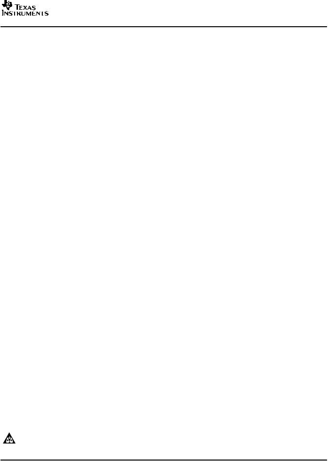
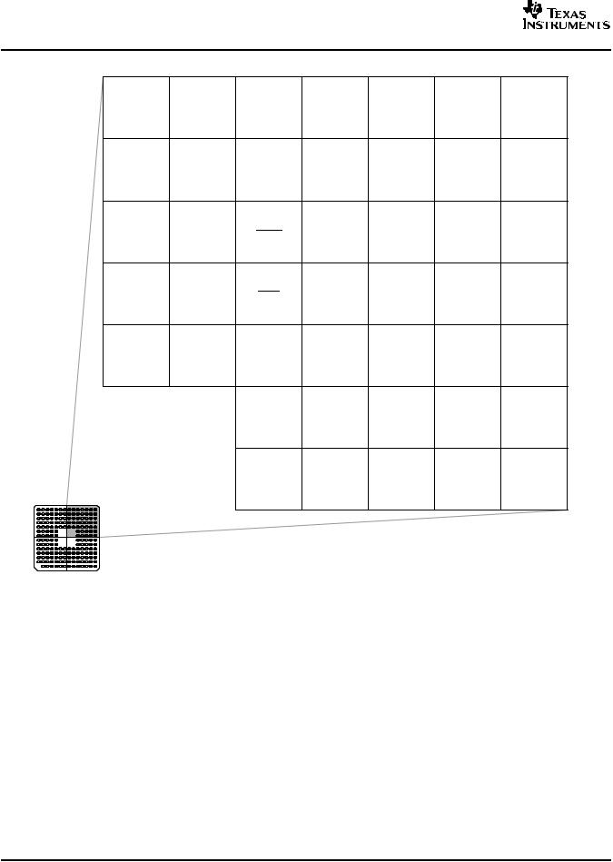
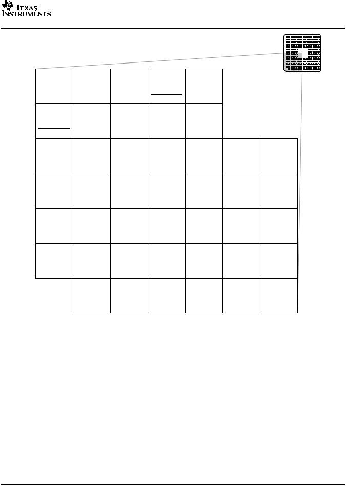
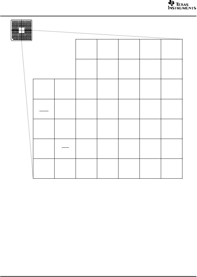
2.1Pin Assignments
The 176-pin PZ low-profile quad flatpack (LQFP) pin assignments are shown in Figure 2-1. The 179-ball ZHH ball grid array (BGA) terminal assignments are shown in Figure 2-2 through Figure 2-5. Table 2-2 describes the function(s) of each pin.
PRODUCT PREVIEW
Submit Documentation Feedback |
Introduction |
9 |

PREVIEW PRODUCT
TMS320F28335, TMS320F28334, TMS320F28332
Digital Signal Controllers (DSCs)
www.ti.com
SPRS439 –JUNE 2007
GPIO76/XD3
GPIO77/XD2
GPIO78/XD1
GPIO79/XD0
GPIO38/XWE0
XCLKOUT
VDD
VSS
GPIO28/SCIRXDA/XZCS6
GPIO34/ECAP1/XREADY
VDDIO
VSS
GPIO36/SCIRXDA/XZCS0 VDD VSS
GPIO35/SCITXDA/XR/W XRD
GPIO37/ECAP2/XZCS7 GPIO40/XA0/XWE1 GPIO41/XA1 GPIO42/XA2
VDD
VSS GPIO43/XA3 GPIO44/XA4 GPIO45/XA5
VDDIO
VSS GPIO46/XA6
GPIO47/XA7
GPIO80/XA8
GPIO81/XA9
GPIO82/XA10
VSS
VDD GPIO83/XA11
GPIO84/XA12
VDDIO
VSS GPIO85/XA13
GPIO86/XA14
GPIO87/XA15
GPIO39/XA16
GPIO31/CANTXA/XA17
133
134
135
136
137
138
139
140
141
142
143
144
145
146
147
148
149
150
151
152
153
154
155
156
157
158
159
160
161
162
163
164
165
166
167
168
169
170
171
172
173
174
175
176
GPIO75/XD4 |
GPIO74/XD5 |
GPIO73/XD6 |
GPIO72/XD7 |
GPIO71/XD8 |
GPIO70/XD9 |
V |
V |
GPIO69/XD10 |
||||||||
|
|
|
|
|
|
|
|
|
|
|
|
DD |
SS |
|
||
|
|
|
|
|
|
|
|
|
|
|
|
|
|
|
|
|
132 |
131 |
130 |
129 |
128 |
127 |
126 |
125 |
124 |
||||||||
1 2 3 4 5 6 7 8 9 |
|||||||||
|
|
|
|
V V |
|
|
|
GPIO2/EPWM2A |
V V |
GPIO30/CANRXA/XA18 GPIO29/SCITXDA/XA19 |
GPIO0/EPWM1A |
GPIO1/EPWM1B/ECAP6/MFSRB |
|||||||
|
|
|
|
SS DD |
|
|
|
|
SS DDIO |
GPIO68/XD11 |
GPIO67/XD12 |
V |
V |
GPIO66/XD13 |
V |
V |
||||||
|
|
|
|
DDIO |
SS |
|
|
SS |
DD |
|||
|
|
|
|
|
|
|
|
|
|
|
|
|
123 |
122 |
121 |
120 |
119 |
118 |
117 |
||||||
10 11 12 13 14 15 16 |
||||||||||
GPIO3/EPWM2B/ECAP5/MCLKRB |
|
|
|
|
|
|
|
|
V |
GPIO7/EPWM4B/MCLKRA/ECAP2 |
GPIO4/EPWM3A GPIO5/EPWM3B/MFSRA/ECAP1 GPIO6/EPWM4A/EPWMSYNCI/EPWMSYNCO |
V |
|||||||||
|
|
|
|
|
|
|
SS |
DD |
|
|
GPIO65/XD14 |
GPIO64/XD15 |
GPIO63/SCITXDC/XD16 |
GPIO62/SCIRXDC/XD17 |
GPIO61/MFSRB/XD18 |
GPIO60/MCLKRB/XD19 |
GPIO59/MFSRA/XD20 |
V |
V |
V |
|||||||||
|
|
|
|
|
|
|
|
|
|
|
|
|
|
DD |
SS |
DDIO |
||
|
|
|
|
|
|
|
|
|
|
|
|
|
|
|
|
|
|
|
116 |
|
115 |
|
114 |
113 |
112 |
111 |
110 |
109 |
108 |
107 |
|||||||
17 18 19 20 21 22 23 24 25 26 |
||||||||||
|
|
|
|
GPIO11/EPWM6B/SCIRXDB/ECAP4 GPIO12/TZ1/CANTXB/MDXB |
|
|
|
|
/XHOLD/GPIO14/TZ3SCITXDB/MCLKXB |
GPIO15/TZ4/XHOLDA/SCIRXDB/MFSXB |
GPIO8/EPWM5A/CANTXB/ADCSOCAO GPIO9/EPWM5B/SCITXDB/ECAP3 GPIO10/EPWM6A/CANRXB/ADCSOCBO |
V |
V |
GPIO13/TZ2/CANRXB/MDRB |
|||||||
|
|
|
|
|
SS |
DD |
|
|
|
|
V |
XCLKIN X1 V X2 |
V GPIO58/MCLKRA/XD21 |
|
GPIO57/SPISTEA/XD22 GPIO56/SPICLKA/XD23 |
|||||||||||||
|
|||||||||||||||||
|
|||||||||||||||||
SS |
|
|
|
|
SS |
DD |
|
|
|
||||||||
|
|
|
|
|
|
|
|
|
|
|
|
|
|
|
|
|
|
106 105 104 103 102 101 100 |
|
99 98 |
|||||||||||||||
27 28 29 30 31 32 33 34 35 |
|||||||||||
|
|
|
|
|
|
|
|
|
|
|
|
|
|
DD |
SS |
DD1A18 |
SS1AGND |
SSA2 |
DDA2 |
ADCINA7 |
|||
|
|
||||||||||
GPIO16/SPISIMOA/CANTXB/TZ5 GPIO17/SPISOMIA/CANRXB/TZ6 |
V |
V |
|||||||||
V |
V |
V |
V |
||||||||
GPIO55/SPISOMIA/XD24 GPIO54/SPISIMOA/XD25 GPIO53/EQEP1I/XD26 GPIO52/EQEP1S/XD27 V |
V GPIO51/EQEP1B/XD28 |
GPIO50/EQEP1A/XD29 GPIO49/ECAP6/XD30 |
||||||||||||||
|
|
|
|
|
|
|
|
DDIO |
|
SS |
|
|
|
|
||
|
|
|
|
|
|
|
|
|
|
|
|
|
|
|
|
|
97 96 95 94 93 92 91 90 89 |
||||||||||||||||
36 37 38 39 40 41 42 43 44 |
||||||||||
|
|
|
|
|
|
|
|
|
ADCLO |
V |
ADCINA6 ADCINA5 ADCINA4 ADCINA3 ADCINA2 ADCINA1 ADCINA0 |
||||||||||
|
|
|
|
|
|
|
|
|
|
SSAIO |
88  GPIO48/ECAP5/XD31
87  TCK
TCK
86  EMU1
EMU1
85  EMU0
EMU0
84  VDD3VFL
83  VSS
VSS
82  TEST2
TEST2
81  TEST1
TEST1
80  XRS
XRS
79  TMS
TMS
78  TRST
TRST
77  TDO
TDO
76  TDI
TDI
75  GPIO33/SCLA/EPWMSYNCO/ADCSOCBO
74  GPIO32/SDAA/EPWMSYNCI/ADCSOCAO
73  GPIO27/ECAP4/EQEP2S/MFSXB
72  GPIO26/ECAP3/EQEP2I/MCLKXB
71  VDDIO
VDDIO
70  VSS
VSS
69  GPIO25/ECAP2/EQEP2B/MDRB
68  GPIO24/ECAP1/EQEP2A/MDXB
67  GPIO23/EQEP1I/MFSXA/SCIRXDB
66  GPIO22/EQEP1S/MCLKXA/SCITXDB
65  GPIO21/EQEP1B/MDRA/CANRXB
64  GPIO20/EQEP1A/MDXA/CANTXB
63  GPIO19/SPISTEA/SCIRXDB/CANTXA
62  GPIO18/SPICLKA/SCITXDB/CANRXA
61  VDD
VDD
60  VSS
VSS
59  VDD2A18
58  VSS2AGND
57  ADCRESEXT
56  ADCREFP
55  ADCREFM
54  ADCREFIN
53  ADCINB7
52  ADCINB6
51  ADCINB5
50  ADCINB4
49  ADCINB3
48  ADCINB2
47  ADCINB1
46  ADCINB0
45  VDDAIO
Figure 2-1. F28335, F28334, F28332 176-Pin PGF LQFP (Top View)
10 |
Introduction |
Submit Documentation Feedback |
TMS320F28335, TMS320F28334, TMS320F28332
Digital Signal Controllers (DSCs)
www.ti.com
SPRS439 –JUNE 2007
|
1 |
2 |
3 |
4 |
5 |
6 |
7 |
|
|
|
|
|
|
|
|
|
GPIO21/ |
|
|
P |
VSSAIO |
ADCINB0 |
ADCINB2 |
ADCINB6 |
ADCREFP |
VSS |
EQEP1B/ |
P |
|
MDRA/ |
|||||||||
|
|
|
|
|
|
|
CANRXB |
|
|
|
|
|
|
|
|
|
GPIO22/ |
|
|
N |
ADCINA1 |
VDDAIO |
ADCINB1 |
ADCINB5 |
ADCREFM |
VDD |
EQEP1S/ |
N |
|
MCLKXA/ |
|||||||||
|
|
|
|
|
|
|
SCITXDB |
|
|
|
|
|
|
|
|
|
GPIO23/ |
|
|
M |
ADCINA2 |
ADCLO |
ADCINA0 |
ADCINB4 |
ADCRESEXT |
VDD2A18 |
EQEP1I/ |
M |
|
MFSXA/ |
|||||||||
|
|
|
|
|
|
|
SCIRXDB |
|
|
|
|
|
|
|
|
GPIO18/ |
GPIO20/ |
|
|
L |
ADCINA5 |
ADCINA4 |
ADCINA3 |
ADCINB3 |
ADCREFIN |
SPICLKA/ |
EQEP1A/ |
L |
|
SCITXDB/ |
MDXA/ |
||||||||
|
|
|
|
|
|
|
|||
|
|
|
|
|
|
CANRXA |
CANTXB |
|
|
|
|
|
|
|
|
|
GPIO19/ |
|
|
K |
VSS1AGND |
VDDA2 |
VSSA2 |
ADCINA7 |
ADCINB7 |
VSS2AGND |
SPISTEA/ |
K |
|
SCIRXDB/ |
|||||||||
|
|
|
|
|
|
|
CANTXA |
|
|
|
GPIO17/ |
|
|
|
|
6 |
7 |
|
|
|
|
|
|
|
|
|
|
||
J |
SPISOMIA/ |
VDD |
VSS |
VDD1A18 |
ADCINA6 |
J |
|
|
|
CANRXB/ |
|
|
|||||||
|
TZ6 |
|
|
|
|
|
|
|
|
|
|
GPIO14/ |
GPIO13/ |
GPIO15/ |
GPIO16/ |
|
|
|
|
H |
VDD |
TZ3 XHOLD/ |
TZ2/ |
TZ4 XHOLDA/ |
SPISIMOA/ |
H |
|
|
|
SCITXDB/ |
CANRXB/ |
SCIRXDB/ |
CANTXB/ |
|
|
||||
|
|
MCLKXB |
MDRB |
MFSXB |
TZ5 |
|
|
|
|
|
1 |
2 |
3 |
4 |
5 |
|
|
|
PRODUCT PREVIEW
Figure 2-2. F28335, F28334, F28332 179-Ball ZHH MicroStar BGA™ (Upper Left Quadrant) (Bottom View)
Submit Documentation Feedback |
Introduction |
11 |
PREVIEW PRODUCT
TMS320F28335, TMS320F28334, TMS320F28332
Digital Signal Controllers (DSCs)
SPRS439 –JUNE 2007 |
|
|
|
|
|
|
www.ti.com |
||
|
|
|
|
|
|
|
|
||
|
8 |
9 |
10 |
11 |
12 |
13 |
14 |
|
|
|
|
GPIO33/ |
|
|
|
GPIO48/ |
GPIO50/ |
|
|
|
|
SCLA/ |
|
|
|
|
|||
P |
VSS |
TMS |
TEST2 |
EMU1 |
ECAP5/ |
EQEP1A/ |
P |
||
EPWMSYNCO/ |
|||||||||
|
|
|
|
|
XD31 |
XD29 |
|
||
|
|
ADCSOCBO |
|
|
|
|
|||
|
|
|
|
|
|
|
|
||
|
GPIO25/ |
GPIO32/ |
|
|
|
GPIO49/ |
|
|
|
|
ECAP2/ |
SDAA/ |
|
|
|
|
|
||
N |
VSS |
VSS |
TCK |
ECAP6/ |
VDDIO |
N |
|||
EQEP2B/ |
EPWMSYNCI/ |
||||||||
|
|
|
|
XD30 |
|
|
|||
|
MDRB |
ADCSOCAO |
|
|
|
|
|
||
|
|
|
|
|
|
|
|||
|
GPIO24/ |
|
|
|
|
GPIO51/ |
GPIO52/ |
|
|
|
ECAP1/ |
|
|
|
|
|
|||
M |
TDI |
TRST |
VDD3VFL |
VSS |
EQEP1B/ |
EQEP1S/ |
M |
||
EQEP2A/ |
|||||||||
|
|
|
|
|
XD28 |
XD27 |
|
||
|
MDXB |
|
|
|
|
|
|||
|
|
|
|
|
|
|
|
||
|
|
GPIO27/ |
|
|
GPIO53/ |
GPIO54/ |
GPIO55/ |
|
|
|
|
ECAP4/ |
|
|
|
||||
L |
VDDIO |
XRS |
EMU0 |
EQEP1I/ |
SPISIMOA/ |
SPISOMIA/ |
L |
||
EQEP2S/ |
|||||||||
|
|
|
|
XD26 |
XD25 |
XD24 |
|
||
|
|
MFSXB |
|
|
|
||||
|
|
|
|
|
|
|
|
||
|
GPIO26/ |
|
|
GPIO56/ |
GPIO58/ |
GPIO57/ |
|
|
|
|
ECAP3/ |
|
|
|
|
||||
K |
TDO |
TEST1 |
SPICLKA/ |
MCLKRA/ |
SPISTEA/ |
VDD |
K |
||
EQEP2I/ |
|||||||||
|
|
|
XD23 |
XD21 |
XD22 |
|
|
||
|
MCLKXB |
|
|
|
|
||||
|
|
|
|
|
|
|
|
||
|
8 |
9 |
|
|
|
|
|
|
|
|
|
J |
VSS |
X2 |
VSS |
X1 |
XCLKIN |
J |
|
|
|
|
|
|
|
|
GPIO59/ |
|
|
|
|
H |
VSS |
VDDIO |
VDD |
VSS |
MFSRA/ |
H |
|
|
|
|
|
|
|
|
XD20 |
|
|
|
|
|
10 |
11 |
12 |
13 |
14 |
|
|
Figure 2-3. F28335, F28334, F28332 179-Ball ZHH MicroStar BGA™ (Upper Right Quadrant) (Bottom View)
12 |
Introduction |
Submit Documentation Feedback |
TMS320F28335, TMS320F28334, TMS320F28332
Digital Signal Controllers (DSCs)
www.ti.com |
|
|
|
|
|
|
SPRS439 –JUNE 2007 |
|
||
|
|
|
|
|
|
|
|
|
||
|
1 |
2 |
3 |
4 |
5 |
|
|
|
|
|
|
|
GPIO11/ |
GPIO12/ |
GPIO10/ |
GPIO9/ |
|
|
|
|
|
G |
VSS |
EPWM6B/ |
TZ1/ |
EPWM6A/ |
EPWM5B/ |
G |
|
|
|
|
SCIRXDB/ |
CANTXB/ |
CANRXB/ |
SCITXDB/ |
|
|
|
||||
|
|
ECAP4 |
MDXB |
ADCSOCBO |
ECAP3 |
|
|
|
|
|
|
GPIO8/ |
GPIO7/ |
|
|
|
|
|
|
|
|
F |
EPWM5A/ |
EPWM4B/ |
VDD |
VSS |
VDDIO |
F |
|
|
|
|
CANTXB/ |
MCLKRA/ |
|
|
|
||||||
|
ADCSOCAO |
ECAP2 |
|
|
|
6 |
7 |
|
|
|
|
GPIO6/ |
|
GPIO5/ |
GPIO3/ |
|
|
|
|
PREVIEW |
|
E |
EPWM4A/ |
GPIO4/ |
EPWM3B/ |
EPWM2B/ |
GPIO84/ |
GPIO81/ |
VDDIO |
E |
||
EPWMSYNCI/ |
EPWM3A |
MFSRA/ |
ECAP5/ |
XA12 |
XA9 |
|||||
|
EPWMSYNCO |
|
ECAP1 |
MCLKRB |
|
|
|
|
||
|
|
|
GPIO1/ |
|
|
|
|
|
||
D |
VSS |
GPIO2/ |
EPWM1B/ |
GPIO86/ |
GPIO83/ |
VSS |
GPIO45/ |
D |
||
EPWM2A |
ECAP6/ |
XA14 |
XA11 |
XA5 |
||||||
|
|
|
MFSRB |
|
|
|
|
|
||
|
|
|
|
|
|
|
|
|
||
|
GPIO0/ |
GPIO29/ |
|
GPIO85/ |
GPIO82/ |
GPIO80/ |
|
|
PRODUCT |
|
C |
SCITXDA/ |
VSS |
VSS |
C |
||||||
EPWM1A |
XA13 |
XA10 |
XA8 |
|||||||
|
XA19 |
|
|
|
||||||
|
|
|
|
|
|
|
|
|||
|
|
GPIO30/ |
GPIO39/ |
|
|
GPIO46/ |
GPIO43/ |
|
||
B |
VDD |
CANRXA/ |
VSS |
VDD |
B |
|||||
XA16 |
XA6 |
XA3 |
||||||||
|
|
XA18 |
|
|
|
|||||
|
|
|
|
|
|
|
|
|||
|
|
|
|
|
|
|
|
|
||
|
|
GPIO31/ |
GPIO87/ |
|
|
GPIO47/ |
GPIO44/ |
|
|
|
A |
|
CANTXA/ |
VDDIO |
VSS |
A |
|
||||
|
XA15 |
XA7 |
XA4 |
|
||||||
|
|
XA17 |
|
|
|
|
||||
|
|
|
|
|
|
|
|
|
||
|
1 |
2 |
3 |
4 |
5 |
6 |
7 |
|
|
|
Figure 2-4. F28335, F28334, F28332 179-Ball ZHH MicroStar BGA™ |
(Lower Left Quadrant) (Bottom View) |
|
||||||||
Submit Documentation Feedback |
Introduction |
13 |
PREVIEW PRODUCT
TMS320F28335, TMS320F28334, TMS320F28332
Digital Signal Controllers (DSCs)
www.ti.com
SPRS439 –JUNE 2007
|
|
|
10 |
11 |
12 |
13 |
14 |
|
|
|
|
|
GPIO64/ |
GPIO63/ |
GPIO61/ |
GPIO62/ |
GPIO60/ |
|
|
|
|
G |
SCITXDC/ |
MFSRB/ |
SCIRXDC |
MCLKRB/ |
G |
||
|
|
XD15 |
|||||||
|
|
|
XD16 |
XD18 |
XD17 |
XD19 |
|
||
|
|
|
|
|
|||||
|
|
F |
GPIO69/ |
GPIO66/ |
VSS |
VDD |
GPIO65/ |
F |
|
|
|
XD10 |
XD13 |
XD14 |
|||||
|
8 |
9 |
|
|
|
|
|
|
|
|
|
|
GPIO28/ |
GPIO68/ |
|
GPIO67/ |
|
|
|
E |
VSS |
VDD |
SCIRXDA/ |
VDDIO |
VSS |
E |
|||
XD11 |
XD12 |
||||||||
|
|
|
XZCS6 |
|
|
|
|||
|
|
|
|
|
|
|
|
||
|
GPIO40/ |
GPIO37/ |
GPIO34/ |
GPIO38/ |
GPIO70/ |
|
|
|
|
D |
XA0/ |
ECAP2/ |
ECAP1/ |
VDD |
VSS |
D |
|||
XWE0 |
XD9 |
||||||||
|
XWE1 |
XZCS7 |
XREADY |
|
|
|
|||
|
|
|
|
|
|
||||
|
|
|
GPIO36/ |
|
GPIO73/ |
GPIO74/ |
GPIO71/ |
|
|
C |
VDD |
VSS |
SCIRXDA/ |
XCLKOUT |
C |
||||
XD6 |
XD5 |
XD8 |
|||||||
|
|
|
XZCS0 |
|
|
||||
|
|
|
|
|
|
|
|
||
B |
GPIO42/ |
XRD |
VDDIO |
VDD |
GPIO78/ |
GPIO76/ |
GPIO72/ |
B |
|
XA2 |
XD1 |
XD3 |
XD7 |
||||||
|
GPIO41/ |
GPIO35/ |
|
|
GPIO79/ |
GPIO77/ |
GPIO75/ |
|
|
A |
SCITXDA/ |
VSS |
VSS |
A |
|||||
XA1 |
XD0 |
XD2 |
XD4 |
||||||
|
XR/W |
|
|
|
|||||
|
|
|
|
|
|
|
|
||
|
8 |
9 |
10 |
11 |
12 |
13 |
14 |
|
|
Figure 2-5. F28335, F28334, F28332 179-Ball ZHH MicroStar BGA™ |
(Lower Right Quadrant) (Bottom View) |
||||||||
14 |
Introduction |
Submit Documentation Feedback |
TMS320F28335, TMS320F28334, TMS320F28332
Digital Signal Controllers (DSCs)
www.ti.com
SPRS439 –JUNE 2007
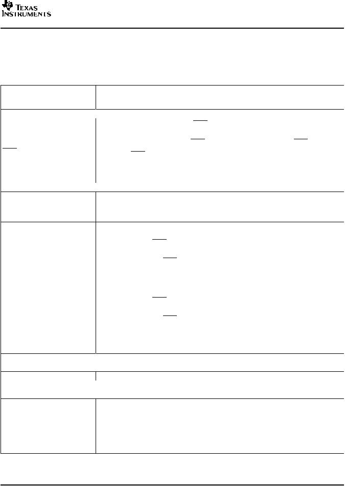
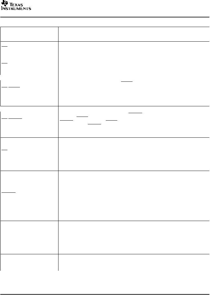
2.2Signal Descriptions
Table 2-2 describes the signals on the 2833x devices. All digital inputs are TTL-compatible. All outputs are 3.3 V with CMOS levels. Inputs are not 5-V tolerant.
|
|
|
Table 2-2. Signal Descriptions |
|
PIN NO. |
|
|
NAME |
PGF |
ZHH |
DESCRIPTION (1) |
|
PIN # |
BALL # |
|
JTAG
TRST |
78 |
M10 |
TCK |
87 |
N12 |
TMS |
79 |
P10 |
TDI |
76 |
M9 |
TDO |
77 |
K9 |
EMU0 |
85 |
L11 |
EMU1 |
86 |
P12 |
VDD3VFL |
84 |
M11 |
TEST1 |
81 |
K10 |
TEST2 |
82 |
P11 |
XCLKOUT |
138 |
C11 |
XCLKIN |
105 |
J14 |
JTAG test reset with internal pulldown. TRST, when driven high, gives the scan system control of the operations of the device. If this signal is not connected or driven low, the device operates in its functional mode, and the test reset signals are ignored.
NOTE: Do not use pullup resistors on TRST; it has an internal pull-down device. TRST is an active high test pin and must be maintained low at all times during normal device operation. In a low-noise environment, TRST may be left floating. In other instances, an external pulldown resistor is highly recommended. The value of this resistor should be based on drive strength of the debugger pods applicable to the design. A 2.2-kΩ resistor generally offers adequate protection. Since this is application-specific, it is recommended that each target board be validated for proper operation of the debugger and the application. (I, ↓)
 JTAG test clock with internal pullup (I, −)
JTAG test-mode select (TMS) with internal pullup. This serial control input is clocked into the TAP controller on the rising edge of TCK. (I, −)
JTAG test data input (TDI) with internal pullup. TDI is clocked into the selected register (instruction or data) on a rising edge of TCK. (I, −)
JTAG scan out, test data output (TDO). The contents of the selected register (instruction or data) are shifted out of TDO on the falling edge of TCK. (O/Z 8 mA drive)
Emulator pin 0. When TRST is driven high, this pin is used as an interrupt to or from the emulator system and is defined as input/output through the JTAG scan. This pin is also used to put the device into boundary-scan mode. With the EMU0 pin at a logic-high state and the EMU1 pin at a logic-low state, a rising edge on the TRST pin would latch the device into boundary-scan mode. (I/O/Z, 8 mA drive −)
NOTE: An external pullup resistor is recommended on this pin. The value of this resistor should be based on the drive strength of the debugger pods applicable to the design. A 2.2-kΩ to 4.7-kΩ resistor is generally adequate. Since this is application-specific, it is recommended that each target board be validated for proper operation of the debugger and the application.
Emulator pin 1. When TRST is driven high, this pin is used as an interrupt to or from the emulator system and is defined as input/output through the JTAG scan. This pin is also used to put the device into boundary-scan mode. With the EMU0 pin at a logic-high state and the EMU1 pin at a logic-low state, a rising edge on the TRST pin would latch the device into boundary-scan mode. (I/O/Z, 8 mA drive −)
NOTE: An external pullup resistor is recommended on this pin. The value of this resistor should be based on the drive strength of the debugger pods applicable to the design. A 2.2-kΩ to 4.7-kΩ resistor is generally adequate. Since this is application-specific, it is recommended that each target board be validated for proper operation of the debugger and the application.
FLASH
 3.3-V Flash Core Power Pin. This pin should be connected to 3.3 V at all times.
Test Pin. Reserved for TI. Must be left unconnected. (I/O)
 Test Pin. Reserved for TI. Must be left unconnected. (I/O)
CLOCK
Output clock derived from SYSCLKOUT. XCLKOUT is either the same frequency, one-half the frequency, or one-fourth the frequency of SYSCLKOUT. This is controlled by the bits 1, 0 (XCLKOUTDIV) in the XCLK register. At reset, XCLKOUT = SYSCLKOUT/4. The XCLKOUT signal can be turned off by setting XCLKOUTDIV to 3. Unlike other GPIO pins, the XCLKOUT pin is not placed in high-impedance state during a reset. (O/Z, 8 mA drive).
External Oscillator Input. This pin is to feed a clock from an external 3.3-V oscillator. In this case, the X1 pin must be tied to GND. If a crystal/resonator is used (or if an external 1.8-V oscillator is used to feed clock to X1 pin), this pin must be tied to GND. (I)
PRODUCT PREVIEW
(1)I = Input, O = Output, Z = High impedance, OD = Open drain, − = Pullup, ↓ = Pulldown
Submit Documentation Feedback |
Introduction |
15 |

PREVIEW PRODUCT
TMS320F28335, TMS320F28334, TMS320F28332
Digital Signal Controllers (DSCs)
www.ti.com
SPRS439 –JUNE 2007
Table 2-2. Signal Descriptions (continued)
|
PIN NO. |
|
NAME |
PGF |
ZHH |
|
PIN # |
BALL # |
X1 |
104 |
J13 |
DESCRIPTION (1)
Internal/External Oscillator Input. To use the internal oscillator, a quartz crystal or a ceramic resonator may be connected across X1 and X2. The X1 pin is referenced to the 1.8-V core digital power supply. A 1.8-V external oscillator may be connected to the X1 pin. In this case, the XCLKIN pin must be connected to ground. If a 3.3-V external oscillator is used with the XCLKIN pin, X1 must be tied to GND. (I)
X2 |
102 |
J11 |
Internal Oscillator Output. A quartz crystal or a ceramic resonator may be connected across X1 and |
|
X2. If X2 is not used it must be left unconnected. (O) |
||||
|
|
|
||
|
|
|
RESET |
|
|
|
|
Device Reset (in) and Watchdog Reset (out). |
|
|
|
|
Device reset. XRS causes the device to terminate execution. The PC will point to the address |
|
|
|
|
contained at the location 0x3FFFC0. When XRS is brought to a high level, execution begins at the |
|
XRS |
80 |
L10 |
location pointed to by the PC. This pin is driven low by the DSC when a watchdog reset occurs. |
|
During watchdog reset, the XRS pin is driven low for the watchdog reset duration of 512 OSCCLK |
||||
|
|
|
||
|
|
|
cycles. (I/OD, −) |
|
|
|
|
The output buffer of this pin is an open-drain with an internal pullup. It is recommended that this pin |
|
|
|
|
be driven by an open-drain device. |
|
|
|
|
ADC SIGNALS |
|
ADCINA7 |
35 |
K4 |
ADC Group A, Channel 7 input (I) |
|
ADCINA6 |
36 |
J5 |
ADC Group A, Channel 6 input (I) |
|
ADCINA5 |
37 |
L1 |
ADC Group A, Channel 5 input (I) |
|
ADCINA4 |
38 |
L2 |
ADC Group A, Channel 4 input (I) |
|
ADCINA3 |
39 |
L3 |
ADC Group A, Channel 3 input (I) |
|
ADCINA2 |
40 |
M1 |
ADC Group A, Channel 2 input (I) |
|
ADCINA1 |
41 |
N1 |
ADC Group A, Channel 1 input (I) |
|
ADCINA0 |
42 |
M3 |
ADC Group A, Channel 0 input (I) |
|
ADCINB7 |
53 |
K5 |
ADC Group B, Channel 7 input (I) |
|
ADCINB6 |
52 |
P4 |
ADC Group B, Channel 6 input (I) |
|
ADCINB5 |
51 |
N4 |
ADC Group B, Channel 5 input (I) |
|
ADCINB4 |
50 |
M4 |
ADC Group B, Channel 4 input (I) |
|
ADCINB3 |
49 |
L4 |
ADC Group B, Channel 3 input (I) |
|
ADCINB2 |
48 |
P3 |
ADC Group B, Channel 2 input (I) |
|
ADCINB1 |
47 |
N3 |
ADC Group B, Channel 1 input (I) |
|
ADCINB0 |
46 |
P2 |
ADC Group B, Channel 0 input (I) |
|
ADCLO |
43 |
M2 |
Low Reference (connect to analog ground) (I) |
|
ADCRESEXT |
57 |
M5 |
ADC External Current Bias Resistor. Connect a 22-kΩ resistor to analog ground. |
|
ADCREFIN |
54 |
L5 |
External reference input (I) |
|
ADCREFP |
56 |
P5 |
Internal Reference Positive Output. Requires a low ESR (50 mΩ - 1.5 Ω) ceramic bypass capacitor |
|
of 2.2 μF to analog ground. (O) |
||||
|
|
|
||
ADCREFM |
55 |
N5 |
Internal Reference Medium Output. Requires a low ESR (50 mΩ - 1.5 Ω) ceramic bypass capacitor |
|
of 2.2 μF to analog ground. (O) |
||||
|
|
|
||
|
|
|
CPU AND I/O POWER PINS |
|
VDDA2 |
34 |
K2 |
ADC Analog Power Pin |
|
VSSA2 |
33 |
K3 |
ADC Analog Ground Pin |
|
VDDAIO |
45 |
N2 |
ADC Analog I/O Power Pin |
|
VSSAIO |
44 |
P1 |
ADC Analog I/O Ground Pin |
|
VDD1A18 |
31 |
J4 |
ADC Analog Power Pin |
|
VSS1AGND |
32 |
K1 |
ADC Analog Ground Pin |
|
VDD2A18 |
59 |
M6 |
ADC Analog Power Pin |
|
VSS2AGND |
58 |
K6 |
ADC Analog Ground Pin |
16 |
Introduction |
Submit Documentation Feedback |

|
|
|
TMS320F28335, TMS320F28334, TMS320F28332 |
|
www.ti.com |
|
|
Digital Signal Controllers (DSCs) |
|
|
|
SPRS439 –JUNE 2007 |
||
|
|
|
||
|
|
|
Table 2-2. Signal Descriptions (continued) |
|
|
PIN NO. |
|
||
NAME |
PGF |
ZHH |
DESCRIPTION (1) |
|
|
PIN # |
BALL # |
|
|
VDD |
4 |
B1 |
|
|
VDD |
15 |
B5 |
|
|
VDD |
23 |
B11 |
|
|
VDD |
29 |
C8 |
|
|
VDD |
61 |
D13 |
|
|
VDD |
101 |
E9 |
|
|
VDD |
109 |
F3 |
CPU and Logic Digital Power Pins |
|
VDD |
117 |
F13 |
|
|
VDD |
126 |
H1 |
|
|
VDD |
139 |
H12 |
|
|
VDD |
146 |
J2 |
|
|
VDD |
154 |
K14 |
|
|
VDD |
167 |
N6 |
|
|
VDDIO |
9 |
A4 |
|
|
VDDIO |
71 |
B10 |
|
|
VDDIO |
93 |
E7 |
|
|
VDDIO |
107 |
E12 |
Digital I/O Power Pin |
|
VDDIO |
121 |
F5 |
||
|
||||
VDDIO |
143 |
L8 |
|
|
VDDIO |
159 |
H11 |
|
|
VDDIO |
170 |
N14 |
|
|
VSS |
3 |
A5 |
|
|
VSS |
8 |
A10 |
|
|
VSS |
14 |
A11 |
|
|
VSS |
22 |
B4 |
|
|
VSS |
30 |
C3 |
|
|
VSS |
60 |
C7 |
|
|
VSS |
70 |
C9 |
|
|
VSS |
83 |
D1 |
|
|
VSS |
92 |
D6 |
|
|
VSS |
103 |
D14 |
|
|
VSS |
106 |
E8 |
|
|
VSS |
108 |
E14 |
Digital Ground Pins |
|
VSS |
118 |
F4 |
||
|
||||
VSS |
120 |
F12 |
|
|
VSS |
125 |
G1 |
|
|
VSS |
140 |
H10 |
|
|
VSS |
144 |
H13 |
|
|
VSS |
147 |
J3 |
|
|
VSS |
155 |
J10 |
|
|
VSS |
160 |
J12 |
|
|
VSS |
166 |
M12 |
|
|
VSS |
171 |
N10 |
|
|
VSS |
|
N11 |
|
|
VSS |
|
P6 |
|
|
PRODUCT PREVIEW
Submit Documentation Feedback |
Introduction |
17 |

PREVIEW PRODUCT
TMS320F28335, TMS320F28334, TMS320F28332
Digital Signal Controllers (DSCs)
www.ti.com
SPRS439 –JUNE 2007
|
|
|
Table 2-2. Signal Descriptions (continued) |
|
PIN NO. |
|
|
NAME |
PGF |
ZHH |
DESCRIPTION (1) |
|
PIN # |
BALL # |
|
VSS |
|
P8 |
Digital Ground Pins |
|
|
|
GPIOA AND PERIPHERAL SIGNALS(2) (3) |
GPIO0
EPWM1A
-
-
GPIO1
EPWM1B
ECAP6
MFSRB
GPIO2
EPWM2A
-
-
GPIO3
EPWM2B
ECAP5
MCLKRB
GPIO4
EPWM3A
-
-
GPIO5
EPWM3B
MFSRA
ECAP1
GPIO6
EPWM4A EPWMSYNCI EPWMSYNCO
GPIO7
EPWM4B
MCLKRA
ECAP2
GPIO8
EPWM5A
CANTXB ADCSOCAO
GPIO9
EPWM5B
SCITXDB
ECAP3
GPIO10
EPWM6A
CANRXB ADCSOCBO
GPIO11
EPWM6B
SCIRXDB
ECAP4
5C1
6D3
7D2
10E4
11E2
12E3
13E1
16F2
17F1
18G5
19G4
20G2
General purpose input/output 0 (I/O/Z) (4)
Enhanced PWM1 Output A and HRPWM channel (O)
-
-
General purpose input/output 1 (I/O/Z)(4) Enhanced PWM1 Output B (O) Enhanced Capture 6 input/output (I/O) McBSP-B receive frame synch (I/O)
General purpose input/output 2 (I/O/Z)(4)
Enhanced PWM2 Output A and HRPWM channel (O)
-
-
General purpose input/output 3 (I/O/Z)(4) Enhanced PWM2 Output B (O) Enhanced Capture 5 input/output (I/O) McBSP-B clock receive (I/O)
General purpose input/output 4 (I/O/Z)(4)
Enhanced PWM3 output A and HRPWM channel (O)
-
-
General purpose input/output 5 (I/O/Z)(4) Enhanced PWM3 output B (O) McBSP-A receive frame synch (I/O) Enhanced Capture input/output 1 (I/O)
General purpose input/output 6 (I/O/Z)(4)
Enhanced PWM4 output A and HRPWM channel (O) External ePWM sync pulse input (I)
External ePWM sync pulse output (O)
General purpose input/output 7 (I/O/Z)(4) Enhanced PWM4 output B (O) McBSP-A Clock Receive (I/O) Enhanced capture input/output 2 (I/O)
General Purpose Input/Output 8 (I/O/Z)(4) Enhanced PWM5 output A (O) Enhanced CAN-B transmit (O)
ADC start-of-conversion A (O)
General purpose input/output 9 (I/O/Z)(4) Enhanced PWM5 output B (O)
SCI-B transmit data(O)
Enhanced capture input/output 3 (I/O)
General purpose input/output 10 (I/O/Z)(4) Enhanced PWM6 output A (O)
Enhanced CAN-B receive (I) ADC start-of-conversion B (O)
General purpose input/output 11 (I/O/Z)(4) Enhanced PWM6 output B (O)
SCI-B receive data (I)
Enhanced CAP Input/Output 4 (I/O)
(2)Some peripheral functions may not be available in all devices. See Table 2-1 for details.
(3)All GPIO pins are I/O/Z, 4-mA drive typical (unless otherwise indicated), and have an internal pullup, which can be selectively enabled/disabled on a per-pin basis. This feature only applies to the GPIO pins. The GPIO function (shown in Italics) is the default at reset. The peripheral signals that are listed under them are alternate functions.
(4)The pullups on GPIO0-GPIO11 pins are not enabled at reset.
18 |
Introduction |
Submit Documentation Feedback |
www.ti.com
NAME
GPIO12
TZ1
CANTXB
MDXB
GPIO13
TZ2
CANRXB
MDRB
 GPIO14
TZ3/XHOLD
SCITXDB
MCLKXB
 GPIO15
TZ4/XHOLDA
SCIRXDB
MFSXB
GPIO16
SPISIMOA
CANTXB
TZ5
GPIO17
SPISOMIA
CANRXB
TZ6
GPIO18
SPICLKA
SCITXDB
CANRXA
GPIO19
SPISTEA
SCIRXDB
CANTXA
GPIO20
EQEP1A
MDXA
CANTXB
GPIO21
EQEP1B
MDRA
CANRXB
GPIO22
EQEP1S
MCLKXA
SCITXDB
GPIO23
EQEP1I
MFSXA
SCIRXDB
PIN NO.
PGF |
ZHH |
PIN # |
BALL # |
21 G3
24H3
25H2
26H4
27H5
28J1
62L6
63K7
64L7
65P7
66N7
67M7
TMS320F28335, TMS320F28334, TMS320F28332
Digital Signal Controllers (DSCs)
SPRS439 –JUNE 2007
Table 2-2. Signal Descriptions (continued)
DESCRIPTION (1)
General purpose input/output 12 (I/O/Z)(5)
Trip Zone input 1 (I)
Enhanced CAN-B transmit (O)
McBSP-B transmit serial data (O)
General purpose input/output 13 (I/O/Z)(5)
Trip Zone input 2 (I)
Enhanced CAN-B receive (I)
McBSP-B receive serial data (I)
General purpose input/output 14 (I/O/Z)(5)
Trip Zone input 3/External Hold Request. XHOLD, when active (low), requests the external memory interface (XINTF) to release the external bus and place all buses and strobes into a high-impedance state. The XINTF will release the bus when any current access is complete and there are no pending accesses on the XINTF. (I)
SCI-B Transmit (I)
McBSP-B clock transmit (I/O)
General purpose input/output 15 (I/O/Z)(5)
Trip Zone input 4/External Hold Acknowledge. XHOLDA is driven active (low) when the XINTF has granted an XHOLD request. All XINTF buses and strobe signals will be in a high-impedance state. XHOLDA is released when the XHOLD signal is released. External devices should only drive the external bus when XHOLDA is active (low). (I)
SCI-B receive (I)
McBSP-B transmit frame synch (I/O)
General purpose input/output 16 (I/O/Z)(5)
SPI slave in, master out (I/O)
Enhanced CAN-B transmit (O)
Trip Zone input 5 (I)
General purpose input/output 17 (I/O/Z)(5)
SPI-A slave out, master in (I/O)
Enhanced CAN-B receive (I)
Trip zone input 6 (I)
General purpose input/output 18 (I/O/Z)(5)
SPI-A clock input/output (I/O)
SCI-B transmit (O)
Enhanced CAN-A receive (I)
General purpose input/output 19 (I/O/Z)(5)
SPI-A slave transmit enable input/output (I/O)
SCI-B receive (I)
Enhanced CAN-A transmit (O)
General purpose input/output 20 (I/O/Z)(5)
Enhanced QEP1 input A (I)
McBSP-A transmit serial data (O)
Enhanced CAN-B transmit (O)
General purpose input/output 21 (I/O/Z)(5)
Enhanced QEP1 input B (I)
McBSP-A receive serial data (I)
Enhanced CAN-B receive (I)
General purpose input/output 22 (I/O/Z)(5)
Enhanced QEP1 strobe (I/O)
McBSP-A clock transmit (I/O)
SCI-B transmit (O)
General purpose input/output 23 (I/O/Z)(5)
Enhanced QEP1 index (I/O)
McBSP-A transmit frame synch (I/O)
SCI-B receive (I)
PRODUCT PREVIEW
(5)The pullups on GPIO12-GPIO34 are enabled upon reset.
Submit Documentation Feedback |
Introduction |
19 |

PREVIEW PRODUCT
TMS320F28335, TMS320F28334, TMS320F28332
Digital Signal Controllers (DSCs)
www.ti.com
SPRS439 –JUNE 2007
|
|
|
Table 2-2. Signal Descriptions (continued) |
|
PIN NO. |
|
|
NAME |
PGF |
ZHH |
DESCRIPTION (1) |
|
PIN # |
BALL # |
|
GPIO24
ECAP1
EQEP2A
MDXB
GPIO25
ECAP2
EQEP2B
MDRB
GPIO26
ECAP3
EQEP2I
MCLKXB
GPIO27
ECAP4
EQEP2S
MFSXB
GPIO28
SCIRXDA
XZCS6
GPIO29
SCITXDA
XA19
GPIO30
CANRXA
XA18
GPIO31
CANTXA
XA17
GPIO32
SDAA EPWMSYNCI ADCSOCAO
GPIO33
SCLA EPWMSYNCO ADCSOCBO
GPIO34
ECAP1
XREADY
GPIO35
SCITXDA
XR/W
GPIO36
SCIRXDA
XZCS0
GPIO37
ECAP2
XZCS7
GPIO38
-
XWE0
GPIO39
-
XA016
GPIO40
-
XA0/XWE1
|
|
General purpose input/output 24 (I/O/Z)(5) |
|
68 |
M8 |
Enhanced capture 1 (I/O) |
|
Enhanced QEP2 input A (I) |
|||
|
|
||
|
|
McBSP-B transmit serial data (O) |
|
|
|
General purpose input/output 25 (I/O/Z)(5) |
|
69 |
N8 |
Enhanced capture 2 (I/O) |
|
Enhanced QEP2 input B (I) |
|||
|
|
||
|
|
McBSP-B receive serial data (I) |
|
|
|
General purpose input/output 26 (I/O/Z)(5) |
|
72 |
K8 |
Enhanced capture 3 (I/O) |
|
Enhanced QEP2 index (I/O) |
|||
|
|
||
|
|
McBSP-B clock transmit (O) |
|
|
|
General purpose input/output 27 (I/O/Z)(5) |
|
73 |
L9 |
Enhanced capture 4 (I/O) |
|
Enhanced QEP2 strobe (I/O) |
|||
|
|
||
|
|
McBSP-B transmit frame synch (I/O) |
|
|
|
General purpose input/output 28 (I/O/Z)(5) |
|
141 |
E10 |
SCI receive data (I) |
|
|
|
External memory interface zone 6 chip select (O) |
|
|
|
General purpose input/output 29. (I/O/Z)(5) |
|
2 |
C2 |
SCI transmit data (O) |
|
|
|
External Memory Interface Address Line 19 (O) |
|
|
|
General purpose input/output 30 (I/O/Z)(5) |
|
1 |
B2 |
Enhanced CAN-A receive (I) |
|
|
|
External Memory Interface Address Line 18 (O) |
|
|
|
General purpose input/output 31 (I/O/Z)(5) |
|
176 |
A2 |
Enhanced CAN-A transmit (O) |
|
|
|
External Memory Interface Address Line 17 (O) |
|
|
|
General purpose input/output 32 (I/O/Z)(5) |
|
74 |
N9 |
I2C data open-drain bidirectional port (I/OD) |
|
Enhanced PWM external sync pulse input (I) |
|||
|
|
||
|
|
ADC start-of-conversion A (O) |
|
|
|
General-Purpose Input/Output 33 (I/O/Z)(5) |
|
75 |
P9 |
I2C clock open-drain bidirectional port (I/OD) |
|
Enhanced PWM external synch pulse output (O) |
|||
|
|
||
|
|
ADC start-of-conversion B (O) |
|
|
|
General-Purpose Input/Output 34 (I/O/Z)(5) |
|
142 |
D10 |
Enhanced Capture input/output 1 (I/O) |
|
|
|
External memory interface Ready signal |
|
|
|
General-Purpose Input/Output 35 (I/O/Z) |
|
148 |
A9 |
SCI-A transmit data (O) |
|
|
|
External memory interface read, not write strobe |
|
|
|
General-Purpose Input/Output 36 (I/O/Z) |
|
145 |
C10 |
SCI receive data (I) |
|
|
|
External memory interface zone 0 chip select (O) |
|
|
|
General-Purpose Input/Output 37 (I/O/Z) |
|
150 |
D9 |
Enhanced Capture input/output 2 (I/O) |
|
|
|
External memory interface zone 7 chip select (O) |
|
|
|
General-Purpose Input/Output 38 (I/O/Z) |
|
137 |
D11 |
- |
|
|
|
External memory interface Write Enable 0 (O) |
|
|
|
General-Purpose Input/Output 39 (I/O/Z) |
|
175 |
B3 |
- |
|
|
|
External Memory Interface Address Line 16 (O) |
|
|
|
General-Purpose Input/Output 40 (I/O/Z) |
|
151 |
D8 |
- |
|
|
|
External Memory Interface Address Line 0/External memory interface Write Enable 1 (O) |
20 |
Introduction |
Submit Documentation Feedback |
|
|
|
TMS320F28335, TMS320F28334, TMS320F28332 |
www.ti.com |
|
|
Digital Signal Controllers (DSCs) |
|
|
SPRS439 –JUNE 2007 |
|
|
|
|
|
|
|
|
Table 2-2. Signal Descriptions (continued) |
|
PIN NO. |
|
|
NAME |
PGF |
ZHH |
DESCRIPTION (1) |
|
PIN # |
BALL # |
|
GPIO41 |
|
|
General-Purpose Input/Output 41 (I/O/Z) |
- |
152 |
A8 |
- |
XA1 |
|
|
External Memory Interface Address Line 1 (O) |
GPIO42 |
|
|
General-Purpose Input/Output 42 (I/O/Z) |
- |
153 |
B8 |
- |
XA2 |
|
|
External Memory Interface Address Line 2 (O) |
GPIO43 |
|
|
General-Purpose Input/Output 43 (I/O/Z) |
- |
156 |
B7 |
- |
XA3 |
|
|
External Memory Interface Address Line 3 (O) |
GPIO44 |
|
|
General-Purpose Input/Output 44 (I/O/Z) |
- |
157 |
A7 |
- |
XA4 |
|
|
External Memory Interface Address Line 4 (O) |
GPIO45 |
|
|
General-Purpose Input/Output 45 (I/O/Z) |
- |
158 |
D7 |
- |
XA5 |
|
|
External Memory Interface Address Line 5 (O) |
GPIO46 |
|
|
General-Purpose Input/Output 46 (I/O/Z) |
- |
161 |
B6 |
- |
XA6 |
|
|
External Memory Interface Address Line 6 (O) |
GPIO47 |
|
|
General-Purpose Input/Output 47 (I/O/Z) |
- |
162 |
A6 |
- |
XA7 |
|
|
External Memory Interface Address Line 7 (O) |
GPIO48 |
|
|
General-Purpose Input/Output 48 (I/O/Z) |
ECAP5 |
88 |
P13 |
Enhanced Capture input/output 5 (I/O) |
XD31 |
|
|
External Memory Interface Data Line 31 (O) |
GPIO49 |
|
|
General-Purpose Input/Output 49 (I/O/Z) |
ECAP6 |
89 |
N13 |
Enhanced Capture input/output 6 (I/O) |
XD30 |
|
|
External Memory Interface Data Line 30 (O) |
GPIO50 |
|
|
General-Purpose Input/Output 50 (I/O/Z) |
EQEP1A |
90 |
P14 |
Enhanced QEP 1input A (I) |
XD29 |
|
|
External Memory Interface Data Line 29 (O) |
GPIO51 |
|
|
General-Purpose Input/Output 51 (I/O/Z) |
EQEP1B |
91 |
M13 |
Enhanced QEP 1input B (I) |
XD28 |
|
|
External Memory Interface Data Line 28 (O) |
GPIO52 |
|
|
General-Purpose Input/Output 52 (I/O/Z) |
EQEP1S |
94 |
M14 |
Enhanced QEP 1Strobe (I/O) |
XD27 |
|
|
External Memory Interface Data Line 27 (O) |
GPIO53 |
|
|
General-Purpose Input/Output 53 (I/O/Z) |
EQEP1I |
95 |
L12 |
Enhanced CAP1 lndex (I/O) |
XD26 |
|
|
External Memory Interface Data Line 26 (O) |
GPIO54 |
|
|
General-Purpose Input/Output 54 (I/O/Z) |
SPISIMOA |
96 |
L13 |
SPI-A slave in, master out (I/O) |
XD25 |
|
|
External Memory Interface Data Line 25 (O) |
GPIO55 |
|
|
General-Purpose Input/Output 55 (I/O/Z) |
SPISOMIA |
97 |
L14 |
SPI-A slave out, master in (I/O) |
XD24 |
|
|
External Memory Interface Data Line 24 (O) |
GPIO56 |
|
|
General-Purpose Input/Output 56 (I/O/Z) |
SPICLKA |
98 |
K11 |
SPI-A clock (I/O) |
XD23 |
|
|
External Memory Interface Data Line 23 (O) |
GPIO57 |
|
|
General-Purpose Input/Output 57 (I/O/Z) |
SPISTEA |
99 |
K13 |
SPI-A slave transmit enable (I/O) |
XD22 |
|
|
External Memory Interface Data Line 22 (O) |
GPIO58 |
|
|
General-Purpose Input/Output 58 (I/O/Z) |
MCLKRA |
100 |
K12 |
McBSP-A receive clock (I/O) |
XD21 |
|
|
External Memory Interface Data Line 21 (O) |
GPIO59 |
|
|
General-Purpose Input/Output 59 (I/O/Z) |
MFSRA |
110 |
H14 |
McBSP-A receive frame synch (I/O) |
XD20 |
|
|
External Memory Interface Data Line 20 (O) |
PRODUCT PREVIEW
Submit Documentation Feedback |
Introduction |
21 |

PREVIEW PRODUCT
TMS320F28335, TMS320F28334, TMS320F28332
Digital Signal Controllers (DSCs)
www.ti.com
SPRS439 –JUNE 2007
|
|
|
Table 2-2. Signal Descriptions (continued) |
|
PIN NO. |
|
|
NAME |
PGF |
ZHH |
DESCRIPTION (1) |
|
PIN # |
BALL # |
|
GPIO60 |
|
|
General-Purpose Input/Output 60 (I/O/Z) |
MCLKRB |
111 |
G14 |
McBSP-B receive clock (I/O) |
XD19 |
|
|
External Memory Interface Data Line 19 (O) |
GPIO61 |
|
|
General-Purpose Input/Output 61 (I/O/Z) |
MFSRB |
112 |
G12 |
McBSP-B receive frame synch (I/O) |
XD18 |
|
|
External Memory Interface Data Line 18 (O) |
GPIO62 |
|
|
General-Purpose Input/Output 62 (I/O/Z) |
SCIRXDC |
113 |
G13 |
SCI-C receive data (I) |
XD17 |
|
|
External Memory Interface Data Line 17 (O) |
GPIO63 |
|
|
General-Purpose Input/Output 63 (I/O/Z) |
SCITXDC |
114 |
G11 |
SCI-C transmit data (O) |
XD16 |
|
|
External Memory Interface Data Line 16 (O) |
GPIO64 |
|
|
General-Purpose Input/Output 64 (I/O/Z) |
- |
115 |
G10 |
- |
XD15 |
|
|
External Memory Interface Data Line 15 (O) |
GPIO65 |
|
|
General-Purpose Input/Output 65 (I/O/Z) |
- |
116 |
F14 |
- |
XD14 |
|
|
External Memory Interface Data Line 14 (O) |
GPIO66 |
|
|
General-Purpose Input/Output 66 (I/O/Z) |
- |
119 |
F11 |
- |
XD13 |
|
|
External Memory Interface Data Line 13 (O) |
GPIO67 |
|
|
General-Purpose Input/Output 67 (I/O/Z) |
- |
122 |
E13 |
- |
XD12 |
|
|
External Memory Interface Data Line 12 (O) |
GPIO68 |
|
|
General-Purpose Input/Output 68 (I/O/Z) |
- |
123 |
E11 |
- |
XD11 |
|
|
External Memory Interface Data Line 11 (O) |
GPIO69 |
|
|
General-Purpose Input/Output 69 (I/O/Z) |
- |
124 |
F10 |
- |
XD10 |
|
|
External Memory Interface Data Line 10 (O) |
GPIO70 |
|
|
General-Purpose Input/Output 70 (I/O/Z) |
- |
127 |
D12 |
- |
XD9 |
|
|
External Memory Interface Data Line 9 (O) |
GPIO71 |
|
|
General-Purpose Input/Output 71 (I/O/Z) |
- |
128 |
C14 |
- |
XD8 |
|
|
External Memory Interface Data Line 8 (O) |
GPIO72 |
|
|
General-Purpose Input/Output 72 (I/O/Z) |
- |
129 |
B14 |
- |
XD7 |
|
|
External Memory Interface Data Line 7 (O) |
GPIO73 |
|
|
General-Purpose Input/Output 73 (I/O/Z) |
- |
130 |
C12 |
- |
XD6 |
|
|
External Memory Interface Data Line 6 (O) |
GPIO74 |
|
|
General-Purpose Input/Output 74 (I/O/Z) |
- |
131 |
C13 |
- |
XD5 |
|
|
External Memory Interface Data Line 5 (O) |
GPIO75 |
|
|
General-Purpose Input/Output 75 (I/O/Z) |
- |
132 |
A14 |
- |
XD4 |
|
|
External Memory Interface Data Line 4 (O) |
GPIO76 |
|
|
General-Purpose Input/Output 76 (I/O/Z) |
- |
133 |
B13 |
- |
XD3 |
|
|
External Memory Interface Data Line 3 (O) |
GPIO77 |
|
|
General-Purpose Input/Output 77 (I/O/Z) |
- |
134 |
A13 |
- |
XD2 |
|
|
External Memory Interface Data Line 2 (O) |
GPIO78 |
|
|
General-Purpose Input/Output 78 (I/O/Z) |
- |
135 |
B12 |
- |
XD1 |
|
|
External Memory Interface Data Line 1 (O) |
22 |
Introduction |
Submit Documentation Feedback |

|
|
|
TMS320F28335, TMS320F28334, TMS320F28332 |
|
www.ti.com |
|
|
Digital Signal Controllers (DSCs) |
|
|
|
SPRS439 –JUNE 2007 |
||
|
|
|
||
|
|
|
Table 2-2. Signal Descriptions (continued) |
|
|
PIN NO. |
|
||
NAME |
PGF |
ZHH |
DESCRIPTION (1) |
|
|
PIN # |
BALL # |
|
|
GPIO79 |
|
|
General-Purpose Input/Output 79 (I/O/Z) |
|
- |
136 |
A12 |
- |
|
XD0 |
|
|
External Memory Interface Data Line 0 (O) |
|
GPIO80 |
|
|
General-Purpose Input/Output 80 (I/O/Z) |
|
- |
163 |
C6 |
- |
|
XA8 |
|
|
External Memory Interface Address Line 8 (O) |
|
GPIO81 |
|
|
General-Purpose Input/Output 81 (I/O/Z) |
|
- |
164 |
E6 |
- |
|
XA9 |
|
|
External Memory Interface Address Line 9 (O) |
|
GPIO82 |
|
|
General-Purpose Input/Output 82 (I/O/Z) |
|
- |
165 |
C5 |
- |
|
XA10 |
|
|
External Memory Interface Address Line 10 (O) |
|
GPIO83 |
|
|
General-Purpose Input/Output 83 (I/O/Z) |
|
- |
168 |
D5 |
- |
|
XA11 |
|
|
External Memory Interface Address Line 11 (O) |
|
GPIO84 |
|
|
General-Purpose Input/Output 84 (I/O/Z) |
|
- |
169 |
E5 |
||
External Memory Interface Address Line 12 (O) |
||||
XA12 |
|
|
||
|
|
|
||
GPIO85 |
|
|
General-Purpose Input/Output 85 (I/O/Z) |
|
- |
172 |
C4 |
- |
|
XA13 |
|
|
External Memory Interface Address Line 13 (O) |
|
GPIO86 |
|
|
General-Purpose Input/Output 86 (I/O/Z) |
|
- |
173 |
D4 |
- |
|
XA14 |
|
|
External Memory Interface Address Line 14 (O) |
|
GPIO87 |
|
|
General-Purpose Input/Output 87 (I/O/Z) |
|
- |
174 |
A3 |
- |
|
XA15 |
|
|
External Memory Interface Address Line 15 (O) |
|
XRD |
149 |
B9 |
External memory interface Read Enable |
|
PRODUCT PREVIEW
Submit Documentation Feedback |
Introduction |
23 |

PREVIEW PRODUCT
TMS320F28335, TMS320F28334, TMS320F28332
Digital Signal Controllers (DSCs)
www.ti.com
SPRS439 –JUNE 2007
3 Functional Overview
M0 SARAM 1Kx16 |
|
|
L0 SARAM 4Kx16 |
|
|
|
|
|
OTP 2Kx16 |
|
|
||
|
(0-Wait) |
|
|
(0-Wait, Dual Map) |
|
|
|
|
|
|
|
|
|
|
|
|
|
|
|
|
|
|
|
|
|||
|
|
|
|
|
|
|
|
|
|
|
|
|
|
M1 SARAM 1Kx16 |
|
|
L1 SARAM 4Kx16 |
|
|
|
|
|
|
|
|
||
|
(0-Wait) |
|
|
(0-Wait, Dual Map) |
|
|
|
|
|
Flash |
|
|
|
|
|
|
|
|
|
|
|
|
|
|
|
|
|
|
|
|
|
|
L2 SARAM 4Kx16 |
|
|
|
|
|
256Kx16 |
|
|
|
|
|
|
|
(0-Wait, Dual Map) |
|
|
Code |
|
|
8 Sectors |
|
|
|
|
|
|
|
|
|
|
Security |
|
|
|
|
|
|
|
|
MemoryBus |
L3 SARAM 4Kx16 |
|
|
|
|
|
||||
|
|
|
|
|
Module |
|
|
|
|
|
|||
|
|
|
|
|
|
|
|
|
|
|
|
||
|
|
|
|
|
(0-Wait, Dual Map) |
|
|
|
|
|
|
|
|
|
|
|
|
|
|
|
|
|
|
|
|
|
TEST2 |
|
|
|
|
|
L4 SARAM 4Kx16 |
|
|
|
|
|
|
|
|
|
|
|
|
|
|
|
|
|
|
|
|||
|
|
|
|
|
(0-W Data, 1-W Prog) |
|
|
|
|
|
Pump |
|
TEST1 |
|
|
|
|
|
|
|
|
|
PSWD |
|
|
||
|
Boot ROM |
|
|
|
L5 SARAM 4Kx16 |
|
|
|
|
|
|
||
|
|
|
|
|
|
|
|
|
|
||||
|
|
|
|
(0-W Data, 1-W Prog) |
|
|
|
|
|
Flash |
|
|
|
|
8Kx16 |
|
|
|
|
|
|
|
|
|
|
|
|
|
|
|
|
L6 SARAM 4Kx16 |
|
|
|
|
|
Wrapper |
|
|
|
|
|
|
|
|
|
|
|
|
|
|
|
||
|
|
|
|
|
|
|
|
|
|
|
|
|
|
|
|
|
|
|
(0-W Data, 1-W Prog) |
|
|
|
|
|
|
|
|
|
|
|
|
|
|
|
|
|
|
|
|
|
|
|
|
|
|
|
|
|
|
|
|
|
|
|
|
|
|
|
|
|
L7 SARAM 4Kx16 |
|
|
|
|
|
|
|
|
|
|
|
|
|
(0-W Data, 1-W Prog) |
|
|
|
|
|
|
|
|
|
|
|
|
|
|
|
|
|
|
|
|
|
|
|
|
|
|
|
Memory Bus |
|
|
|
|
|
|
|
|
|
|
XD31:0 |
|
|
|
|
|
XHOLDA |
|
|
|
|
|
XHOLD |
|
|
|
|
|
XREADY |
|
|
|
88 GPIOs |
GPIO |
XR/W |
XINTF |
|
|
|
|
|
|||
|
MUX |
XZCS0 |
|
|
|
|
|
|
|
||
|
|
|
|
|
|
|
|
XZCS7 |
|
|
|
|
|
XZCS6 |
|
|
|
|
|
XWE0 |
|
MemoryBus |
DMABus |
|
|
XA0/XWE1 |
|
||
|
|
XA19:1 |
|
||
|
|
|
|
||
|
|
XCLKOUT |
|
|
|
|
|
XRD |
|
|
|
88 GPIOs |
GPIO |
8 External Interrupts |
|
|
|
|
|
|
|||
|
|
|
|
|
|
|
MUX |
|
|
|
|
A7:0 |
|
|
|
|
|
B7:0 |
12-Bit |
|
|
|
|
ADC |
|
|
|
|
|
|
DMA Bus |
|
|
||
|
2-S/H |
|
|
||
|
|
|
|
|
|
REFIN |
|
|
|
|
|
16-bit peripheral bus
32-bit peripheral bus (DMA accessible)
|
FPU |
|
|
|
|
|
TCK |
|
|
|
TDI |
|
|
|
TMS |
|
CPU |
|
TDO |
|
(150 MHZ @ 1.9 V) |
||
|
|
||
|
|
|
TRST |
|
|
|
EMU0 |
|
|
|
EMU1 |
|
|
|
XCLKIN |
|
CPU Timer 0 |
OSC, |
X1 |
DMA |
|
||
CPU Timer 1 |
PLL, |
|
|
6 Ch |
LPM, |
X2 |
|
|
|
WD |
XRS |
|
CPU Timer 2 |
|
|
|
PIE |
|
|
|
(Interrupts) |
|
|
Memory Bus
32-bit peripheral bus
|
|
FIFO |
|
|
|
|
FIFO |
|
|
|
|
FIFO |
|
|
|
|
|
|
|
|
|
|
|
|
|
|
|
EPWM-1/../6 |
|
|
|
|
|
|
|
|
|
|
|
|
|
|
||||||||||
(16 Levels) |
|
|
|
(16 Levels) |
(16 Levels) |
|
|
|
|
|
|
|
|
|
|
|
|
|
|
|
|
|
|
|
|
|
|
|
|
|
CAN-A/B |
|||||||||||||||||||||
|
|
|
|
|
|
|
|
|
|
|
|
|
|
|
|
|
|
|
|
|
|
|
|
|
|
|
|
|
|
|
|
|
|
|
||||||||||||||||||
|
|
|
|
|
|
|
|
|
|
|
|
|
|
|
|
|
|
|
|
|
McBSP-A/B |
|
|
|
|
|
|
|
|
|
|
|
|
|
ECAP-1/../6 |
|
EQEP-1/2 |
|||||||||||||||
|
|
|
|
|
|
|
|
|
|
|
|
|
|
|
|
|
|
|
|
|
|
|
|
|
|
|
|
|
|
|
|
|
|
|
(32-mbox) |
|||||||||||||||||
|
|
|
|
|
|
|
|
|
|
|
|
|
|
|
|
|
|
|
|
|
|
|
|
|
|
|
|
|
|
|
|
|
|
|
|
|
|
|
|
|
|
|
|
|
|
|
|
|
||||
SCI-A/B/C |
|
|
|
|
SPI-A |
|
|
|
|
I2C |
|
|
|
|
|
|
|
|
|
|
|
|
|
|
|
HRPWM-1/../6 |
|
|
|
|
|
|
|
|
|
|
|
|
|
|
||||||||||||
|
|
|
|
|
|
|
|
|
|
|
|
|
|
|
|
|
|
|
|
|
|
|
|
|
|
|
|
|
|
|
|
|
|
|
|
|
|
|
|
|
|
|
|
|
|
|
|
|
|
|
|
|
SCITXDx |
|
SCIRXDx |
|
SPISIMOx |
|
SPISOMIx |
|
SPICLKx |
|
SPISTEx |
|
SDAx |
|
SCLx |
|
MDXx |
|
MRXx |
|
MCLKXx |
|
MCLKRx |
|
MFSXx |
|
MFSRx |
|
TZxn |
|
EPWMxA |
|
EPWMxB |
ESYNCI |
|
ESYNCO |
|
ECAPx |
|
EQEPxA |
|
EQEPxB |
|
EQEPxI |
|
EQEPxS |
|
CANRXx |
|
CANTXx |
|
||
|
|
|
|
|
|
|
|
|
|
|
|
|
|
|
|
|
|
|
|
|
|
|
|
|
||||||||||||||||||||||||||||
|
|
|
|
|
|
|
|
|
|
|
|
|
|
|
|
|
|
|
|
|
|
|
|
|
|
|
|
|
|
|
|
|
|
|
|
|
|
|
|
|
|
|
|
|||||||||
|
|
|
|
|
|
|
|
|
|
|
|
|
|
|
|
|
|
|
|
|
|
|
|
|
|
|
|
|
|
|
|
|
|
|
|
|
|
|
|
|
|
|
|
|
|
|
|
|
|
|
|
|
|
|
|
|
|
|
|
|
|
|
|
|
|
|
|
|
|
|
|
|
|
|
|
|
|
GPIO MUX |
|
|
|
|
|
|
|
|
|
|
|
|
|
|
|
|
|
|
|
|
|
|
|||||
|
|
|
|
|
|
|
|
|
|
|
|
|
|
|
|
|
|
|
|
|
|
|
|
|
|
|
|
|
|
|
|
|
|
|
|
|
|
|
|
|
|
|
|
|
|
|
|
|||||
|
|
|
|
|
|
|
|
|
|
|
|
|
|
|
|
|
|
|
|
|
|
|
|
|
|
|
|
|
88 GPIOs |
|
|
|
|
|
|
|
|
|
|
|
|
|
|
|
|
|
|
|||||
Figure 3-1. Functional Block Diagram
24 |
Functional Overview |
Submit Documentation Feedback |

TMS320F28335, TMS320F28334, TMS320F28332
Digital Signal Controllers (DSCs)
www.ti.com
SPRS439 –JUNE 2007
3.1Memory Maps
In Figure 3-2 through Figure 3-4, the following apply:
∙Memory blocks are not to scale.
∙Peripheral Frame 0, Peripheral Frame 1, Peripheral Frame 2, and Peripheral Frame 3 memory maps are restricted to data memory only. A user program cannot access these memory maps in program space.
∙Protected means the order of Write followed by Read operations is preserved rather than the pipeline order.
∙Certain memory ranges are EALLOW protected against spurious writes after configuration.
PRODUCT PREVIEW
Submit Documentation Feedback |
Functional Overview |
25 |
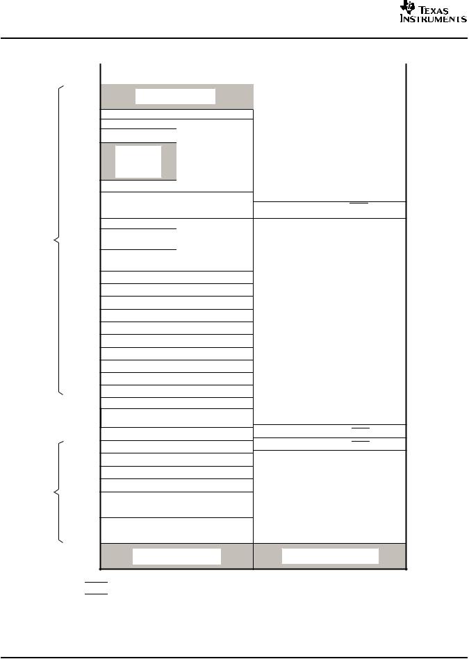
PREVIEW PRODUCT
TMS320F28335, TMS320F28334, TMS320F28332
Digital Signal Controllers (DSCs)
SPRS439 –JUNE 2007
Block |
On-Chip Memory |
External Memory XINTF |
|
Start Address |
|||
|
|
Low64K (24x/240xEquivalentDataSpace)
High64K |
(24x/240xEquivalent |
ProgramSpace) |
0x00 0000
0x00 0040
0x00 0400
0x00 0800
0x00 0D00
0x00 0E00
0x00 2000
0x00 5000
0x00 6000
0x00 7000
0x00 8000
0x00 9000
0x0000-A000
0x0000-B000
0x0000-C000
0x0000-D000
0x0000-E000
0x0000-F000
0x0001-0000
0x30 0000
0x33 FFF8
0x34 0000
0x38 0400 0x3F 8000
0x3F 9000
0x3F A000
0x3F B000 0x3F C000
0x3F E000
0x3F FFC0
Data Space |
Prog Space |
Data Space |
Prog Space |
|
|
|
|
M0 Vector - RAM (32 x 32)
(Enable if VMAP = 0)
M0 SARAM (1K x 16)
M1 SARAM (1K x 16)
Peripheral Frame 0
PIE Vector - RAM
(256 x16)
(Enabled if Reserved VMAP = 1,
ENPIE =1)
Peripheral Frame 0
Reserved
Peripheral Frame 3 (Protected, DMA Accessable)
Peripheral Frame 1
(Protected)
Reserved
Peripheral Frame 2
(Protected)
L0 SARAM (4K x16, Secure Zone Dual Mapped)
L1 SARAM (4K x 16, Secure Zone Dual Mapped)
L2 SARAM (4Kx16, Secure Zone, Dual Mapped)
L3 SARAM (4Kx16, Secure Zone, Dual Mapped)
L4 SARAM (4Kx16, DMA Accessilbe)
L5 SARAM (4Kx16, DMA Accessible)
L6 SARAM (4Kx16, DMA Accessible)
L7 SARAM (4Kx16, DMA Accessiible)
Reserved
FLASH (256 K x 16, Secure Zone)
128-bit Password
Reserved
OTP (IK x 16, Secure Zone)
L0 SARAM (4K x 16, Secure Zone Dual Mapped)
L1 SARAM (4K x 16, Secure Zone Dual Mapped)
L2 SARAM (4K x 16, Secure Zone Dual Mapped)
L3 SARAM (4K x 16, Secure Zone Dual Mapped)
Reserved
Boot ROM (8K x 16)
BROM Vector - ROM (32 x 32) (Enable if VMAP = 1, ENPIE = 0)
Reserved
XINTF Zone 0 (4K x 16,XZCS0)
(Protected, DMA Accessible)
Reserved
XINTF Zone 6 (1 M x 16, XZCS6)
XINTF Zone 7 (1 M x 16, XZCS7)
Reserved
XINTF Vector - RAM (32 x32) (Enable if VMAP = 1, ENPIR = 0)
LEGEND:

 Only one of these vector maps*M0 vector, PIE vector, BROM vector, XINTF vector*should be enabled at a time.
Figure 3-2. F28335 Memory Map
www.ti.com
0x00 4000
0x00 5000
0x10 0000
0x20 0000
0x30 0000
26 |
Functional Overview |
Submit Documentation Feedback |
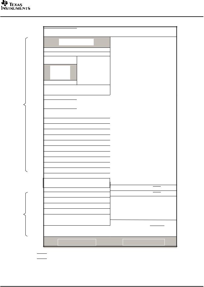
|
|
TMS320F28335, TMS320F28334, TMS320F28332 |
|
www.ti.com |
|
Digital Signal Controllers (DSCs) |
|
|
SPRS439 –JUNE 2007 |
||
|
|
||
Block |
On-Chip Memory |
External Memory XINTF |
|
Start Address |
|||
|
|
Low64K (24x/240xEquivalentDataSpace)
High64K |
(24x/240xEquivalent |
ProgramSpace) |
0x00 0000
0x00 0040
0x00 0400
0x00 0800
0x00 0D00
Peripheral Frame 0
0x00 0E00
0x00 2000
0x00 5000
0x00 6000
0x00 7000
0x00 8000
0x00 9000
0x0000-A000
0x0000-B000
0x0000-C000
0x0000-D000
0x0000-E000
0x0000-F000
0x0001-0000
0x32 0000
0x33 FFF8
0x34 0000
0x38 0400 0x3F 8000
0x3F 9000
0x3F A000
0x3F B000 0x3F C000
0x3F E000
0x3F FFC0
Data Space |
Prog Space |
Data Space |
Prog Space |
|
|
|
|
M0 Vector - RAM (32 x 32)
(Enable if VMAP = 0)
M0 SARAM (1K x 16)
M1 SARAM (1K x 16)
Peripheral Frame 0
Reserved
PIE Vector - RAM
(256 x16) Reserved (Enabled if
VMAP = 1,
ENPIE =1)
Peripheral Frame 0
Reserved |
|
|
|
|
XINTF Zone 0 (4K x 16,XZCS0) |
||||
|
|
(Protected, DMA Accessible) |
||
Peripheral Frame 3 (Protected, DMA Accessable) |
|
|
|
|
Peripheral Frame 1
(Protected)
Reserved
Peripheral Frame 2
(Protected)
L0 SARAM (4K x16, Secure Zone Dual Mapped)
L1 SARAM (4K x 16, Secure Zone Dual Mapped)
L2 SARAM (4Kx16, Secure Zone, Dual Mapped)
L3 SARAM (4Kx16, Secure Zone, Dual Mapped)
L4 SARAM (4Kx16, DMA Accessilbe)
Reserved
L5 SARAM (4Kx16, DMA Accessible)
L6 SARAM (4Kx16, DMA Accessible)
L7 SARAM (4Kx16, DMA Accessiible)
Reserved
FLASH (128 K x 16, Secure Zone)
128-bit Password
Reserved
XINTF Zone 6 (1 M x 16, XZCS6)
OTP (IK x 16, Secure Zone)
XINTF Zone 7 (1 M x 16, XZCS7)
L0 SARAM (4K x 16, Secure Zone Dual Mapped)
L1 SARAM (4K x 16, Secure Zone Dual Mapped)
L2 SARAM (4K x 16, Secure Zone Dual Mapped)
Reserved
L3 SARAM (4K x 16, Secure Zone Dual Mapped)
Reserved
XINTF Zone 7 (16K x 15, XZCS6AND7)
(Enable if MP/MC = 1)
Boot ROM (8K x 16)
|
|
|
|
BROM Vector - ROM (32 x 32) |
|
|
XINTF Vector - RAM (32 x32) |
(Enable if VMAP = 1, ENPIE = 0) |
|
|
(Enable if VMAP = 1, ENPIR = 0) |
|
|
|
|
|
|
|
|
0x00 4000
0x00 5000
0x10 0000
0x20 0000
0x30 0000
LEGEND:

 Only one of these vector maps*M0 vector, PIE vector, BROM vector, XINTF vector*should be enabled at a time.
Figure 3-3. F28334 Memory Map
PRODUCT PREVIEW
Submit Documentation Feedback |
Functional Overview |
27 |

PREVIEW PRODUCT
TMS320F28335, TMS320F28334, TMS320F28332
Digital Signal Controllers (DSCs)
www.ti.com
SPRS439 –JUNE 2007
Block |
On-Chip Memory |
External Memory XINTF |
|
Start Address |
|||
|
|
Low64K (24x/240xEquivalentDataSpace)
High64K |
(24x/240xEquivalent |
ProgramSpace) |
0x00 0000
0x00 0040
0x00 0400
0x00 0800
0x00 0D00
0x00 0E00
0x00 2000
0x00 5000
0x00 6000
0x00 7000
0x00 8000
0x00 9000
0x0000-A000
0x0000-B000
0x0000-C000
0x0000-D000
0x0000-E000
0x33 0000
0x33 FFF8
0x34 0000
0x38 0400 0x3F 8000
0x3F 9000
0x3F A000
0x3F B000 0x3F C000
0x3F E000
0x3F FFC0
|
Data Space |
|
Prog Space |
Data Space |
|
|
|
|
Prog Space |
|||||||||
|
|
|
|
|
|
|
|
|
|
|
|
|
|
|
|
|
|
|
|
|
|
|
|
|
|
|
|
|
|
|
|
|
|
|
|
||
|
|
M0 Vector - RAM (32 x 32) |
|
|
|
|
|
|
|
|
|
|
|
|
|
|||
|
|
(Enable if VMAP = 0) |
|
|
|
|
|
|
|
|
|
|
|
|
|
|||
|
|
|
|
|
|
|
|
|
|
|
|
|
|
|
|
|
|
|
|
|
|
|
|
|
|
|
|
|
|
|
|
|
|
|
|
|
|
|
|
M0 SARAM (1K x 16) |
|
|
|
|
|
|
|
|
|
|
|
|||||
|
|
M1 SARAM (1K x 16) |
|
|
|
|
|
|
|
|
|
|
|
|||||
|
|
|
|
|
|
|
|
|
|
|
|
|
|
|
|
|
|
|
Peripheral Frame 0 |
|
|
|
|
|
|
|
|
|
|
|
|
|
|
|
|||
|
|
|
|
|
|
|
|
|
|
Reserved |
||||||||
|
|
|
|
|
|
|
|
|
|
|
|
|
|
|
|
|
|
|
|
PIE Vector - RAM |
|
|
|
|
|
|
|
|
|
|
|
|
|
|
|
|
|
|
(256 x16) |
|
|
Reserved |
|
|
|
|
|
|
|
|
|
|
|
|||
|
(Enabled if |
|
|
|
|
|
|
|
|
|
|
|
|
|
||||
|
VMAP = 1, |
|
|
|
|
|
|
|
|
|
|
|
|
|
|
|
|
|
|
ENPIE =1) |
|
|
|
|
|
|
|
|
|
|
|
|
|
|
|
|
|
Peripheral Frame 0 |
|
|
|
|
|
|
|
|
|
|
|
|
|
|
|
|||
|
|
|
|
|
|
|
|
|
|
|
|
|
|
|
|
|
|
|
|
|
|
|
|
|
|
|
|
|
|
|
|
|
|
|
|
|
|
|
|
|
|
|
|
|
|
|
|
|
|
|
|
|
|
|||
|
|
|
Reserved |
|
|
|
|
XINTF Zone 0 (4K x 16,XZCS0) |
||||||||||
|
|
|
|
|
|
|
|
|
(Protected, DMA Accessible) |
|||||||||
|
Peripheral Frame 3 (Protected, DMA Accessable) |
|
|
|
|
|
|
|
|
|
|
|
||||||
|
|
|
|
|
|
|
|
|
|
|
|
|
|
|
|
|||
Peripheral Frame 1 |
|
|
|
|
|
|
|
|
|
|
|
|
|
|
|
|||
|
(Protected) |
|
|
|
|
|
|
|
|
|
|
|
|
|
|
|
||
|
|
|
|
|
Reserved |
|
|
|
|
|
|
|
|
|
|
|
||
Peripheral Frame 2 |
|
|
|
|
|
|
|
|
|
|
|
|
||||||
|
|
|
|
|
|
|
|
|
|
|
|
|
|
|
||||
|
(Protected) |
|
|
|
|
|
|
|
|
|
|
|
|
|
|
|
||
|
|
|
|
|
|
|
|
|
|
|
|
|
|
|
|
|||
|
L0 SARAM (4K x16, Secure Zone Dual Mapped) |
|
|
|
|
|
|
|
|
|
|
|
||||||
|
|
|
|
|
|
|
|
|
|
|
|
|
|
|||||
L1 SARAM (4K x 16, Secure Zone Dual Mapped) |
|
|
|
|
|
|
|
|
|
|
|
|||||||
|
|
|
|
|
|
|
|
|
|
|
|
|
||||||
|
L2 SARAM (4Kx16, Secure Zone, Dual Mapped) |
|
|
|
|
|
|
|
|
|
|
|
||||||
|
|
|
|
|
|
|
|
|
|
|
|
|
||||||
|
L3 SARAM (4Kx16, Secure Zone, Dual Mapped) |
|
|
|
|
|
|
|
|
|
|
|
||||||
|
|
|
|
|
|
|
|
|
|
Reserved |
||||||||
|
L4 SARAM (4Kx16, DMA Accessilbe) |
|
|
|
|
|
|
|
|
|
|
|
||||||
|
|
|
|
|
|
|
|
|
|
|
|
|
||||||
|
L5 SARAM (4Kx16, DMA Accessible) |
|
|
|
|
|
|
|
|
|
|
|
||||||
|
|
|
|
|
|
|
|
|
|
|
|
|
|
|
|
|
|
|
|
|
|
Reserved |
|
|
|
|
|
|
|
|
|
|
|
|
|
|
|
|
|
|
|
|
|
|
|
|
|
|
|
|
|
|||||
|
|
FLASH (64 K x 16, Secure Zone) |
|
|
|
|
|
|
|
|
|
|
|
|||||
|
|
128-bit Password |
|
|
|
|
|
|
|
|
|
|
|
|||||
|
|
|
|
|
|
|
|
|
|
|
|
|
|
|
|
|
|
|
|
|
|
Reserved |
|
|
|
|
|
|
|
|
|
|
|
|
|
|
|
|
|
|
|
|
|
|
|
|
|
|
|
|
||||||
|
|
|
|
|
|
|
|
|
|
|
|
|
|
|
|
|
|
|
|
|
|
|
|
|
|
|
|
XINTF Zone 6 (1 M x 16, XZCS6) |
|||||||||
|
|
OTP (IK x 16, Secure Zone) |
|
|||||||||||||||
|
|
|
|
|
|
|
|
|
|
|
|
|
||||||
|
|
|
|
|
|
|
|
|
|
|
|
|
|
|
|
|
|
|
L0 SARAM (4K x 16, Secure Zone Dual Mapped) |
|
XINTF Zone 7 (1 M x 16, XZCS7) |
||||||||||||||||
|
|
|
|
|
|
|
|
|
|
|
||||||||
|
|
|
|
|
|
|
|
|
|
|
|
|||||||
L1 SARAM (4K x 16, Secure Zone Dual Mapped) |
|
|
|
|
|
|
|
|
|
|
|
|||||||
|
|
|
|
|
|
|
|
|
|
|
|
|||||||
L2 SARAM (4K x 16, Secure Zone Dual Mapped) |
|
|
|
|
|
|
|
|
|
|
|
|||||||
|
|
|
|
|
|
|
|
|
|
Reserved |
||||||||
L3 SARAM (4K x 16, Secure Zone Dual Mapped) |
|
|
||||||||||||||||
|
|
|
|
|
|
|
|
|
|
|
||||||||
|
|
|
|
|
|
|
|
|
|
|
|
|
|
|
|
|
|
|
|
|
|
Reserved |
|
|
|
|
|
|
|
|
|
|
|
|
|
|
|
|
|
|
|
|
|
|
|
|
|
|
|
|
|
|
|
|
||
|
|
|
|
|
|
|
|
|
|
|
|
|
|
|
|
|
|
|
|
|
|
|
|
|
|
|
XINTF Zone 7 (16K x 15, XZCS6AND7) |
||||||||||
|
|
Boot ROM (8K x 16) |
|
(Enable if MP/MC = 1) |
||||||||||||||
|
|
|
|
|
|
|
|
|
|
|
|
|
||||||
|
|
|
|
|
|
|
|
|
|
|
|
|
|
|
|
|
|
|
|
|
|
|
|
|
|
|
|
|
|
|
|
|
|
|
|
|
|
|
|
BROM Vector - ROM (32 x 32) |
|
|
XINTF Vector - RAM (32 x32) |
|
||||||||||||
|
|
(Enable if VMAP = 1, ENPIE = 0) |
|
|
(Enable if VMAP = 1, ENPIR = 0) |
|
||||||||||||
|
|
|
|
|
|
|
|
|
|
|
|
|
|
|
|
|
|
|
|
|
|
|
|
|
|
|
|
|
|
|
|
|
|
|
|
|
|
0x00 4000
0x00 5000
0x10 0000
0x20 0000
0x30 0000
LEGEND:

 Only one of these vector maps*M0 vector, PIE vector, BROM vector, XINTF vector*should be enabled at a time.
Figure 3-4. F28332 Memory Map
28 |
Functional Overview |
Submit Documentation Feedback |

TMS320F28335, TMS320F28334, TMS320F28332
Digital Signal Controllers (DSCs)
www.ti.com
SPRS439 –JUNE 2007
Table 3-1. Addresses of Flash Sectors in F28335
ADDRESS RANGE |
PROGRAM AND DATA SPACE |
|
0x30 0000 - 0x30 7FFF |
Sector H (32K x 16) |
|
0x30 8000 - 0x30 FFFF |
Sector G (32K x 16) |
|
0x31 0000 - 0x31 7FFF |
Sector F (32K x 16) |
|
0x31 8000 - 0x31 FFFF |
Sector E (32K x 16) |
|
0x32 0000 - 0x32 7FFF |
Sector D (32K x 16) |
|
0x32 8000 - 0x32 FFFF |
Sector C (32K x 16) |
|
0x33 0000 - 0x33 7FFF |
Sector B (32K x 16) |
|
0x33 8000 - 0x33 FFFF |
Sector A (32K x 16) |
|
0x33 FF80 - 0x33 FFF5 |
Program to 0x0000 when using the |
|
Code Security Module |
||
|
||
0x33 FFF6 - 0x33 FFF7 |
Boot-to-Flash Entry Point |
|
(program branch instruction here) |
||
|
||
0x33 FFF8 - 0x33 FFFF |
Security Password |
|
(128-Bit) (Do Not Program to all zeros) |
||
|
Table 3-2. Addresses of Flash Sectors in F28334
ADDRESS RANGE |
PROGRAM AND DATA SPACE |
0x32 0000 - 0x32 3FFF |
Sector H (16K x 16) |
0x32 4000 - 0x32 7FFF |
Sector G (16K x 16) |
0x32 8000 - 0x32 BFFF |
Sector F (16K x 16) |
0x32 C000 - 0x32 FFFF |
Sector E (16K x 16) |
0x33 0000 - 0x33 3FFF |
Sector D (16K x 16) |
0x33 4000 - 0x33 7FFFF |
Sector C (16K x 16) |
0x33 8000 - 0x33 BFFF |
Sector B (16K x 16) |
0x33 C000 - 0x33 FFFF |
Sector A (16K x 16) |
0x33 FF80 - 0x33 FFF5 |
Program to 0x0000 when using the |
|
Code Security Module |
0x33 FFF6 - 0x33 FFF7 |
Boot-to-Flash Entry Point |
|
(program branch instruction here) |
0x33 FFF8 - 0x33 FFFF |
Security Password (128-Bit) |
|
(Do Not Program to all zeros) |
Table 3-3. Addresses of Flash Sectors in F28332
ADDRESS RANGE |
PROGRAM AND DATA SPACE |
|
0x33 0000 - 0x33 3FFF |
Sector D (16K x 16) |
|
0x33 4000 - 0x33 7FFFF |
Sector C (16K x 16) |
|
0x33 8000 - 0x33 BFFF |
Sector B (16K x 16) |
|
0x33 C000 - 0x33 |
FFFF |
Sector A (16K x 16) |
0x33 FF80 - 0x33 |
FFF5 |
Program to 0x0000 when using the Code Security |
|
|
Module |
0x33 FFF6 - 0x33 FFF7 |
Boot-to-Flash Entry Point (program branch |
|
|
|
instruction here) |
0x33 FFF8 - 0x33 |
FFFF |
Security Password (128-Bit) (Do Not Program to all |
|
|
zeros) |
PRODUCT PREVIEW
Submit Documentation Feedback |
Functional Overview |
29 |

PREVIEW PRODUCT
TMS320F28335, TMS320F28334, TMS320F28332
Digital Signal Controllers (DSCs)
www.ti.com
SPRS439 –JUNE 2007
NOTE
∙When the code-security passwords are programmed, all addresses between 0x33FF80 and 0x33FFF5 cannot be used as program code or data. These locations must be programmed to 0x0000.
∙If the code security feature is not used, addresses 0x33FF80 through 0x33FFEF may be used for code or data. Addresses 0x33FFF0 – 0x33FFF5 are reserved for data and should not contain program code. .
Table 3-4 shows how to handle these memory locations.
Table 3-4. Handling Security Code Locations
ADDRESS |
FLASH |
Code security enabled |
Code security disabled |
0x33FF80 - 0x33FFEF |
Application code and data |
Fill with 0x0000 |
Reserved for data only |
0x33FFF0 - 0x33FFF5 |
Peripheral Frame 1, Peripheral Frame 2, and Peripheral Frame 3 are grouped together to enable these blocks to be write/read peripheral block protected. The protected mode ensures that all accesses to these blocks happen as written. Because of the C28x pipeline, a write immediately followed by a read, to different memory locations, will appear in reverse order on the memory bus of the CPU. This can cause problems in certain peripheral applications where the user expected the write to occur first (as written). The C28x CPU supports a block protection mode where a region of memory can be protected so as to make sure that operations occur as written (the penalty is extra cycles are added to align the operations). This mode is programmable and by default, it will protect the selected zones.
The wait-states for the various spaces in the memory map area are listed in Table 3-5.
30 |
Functional Overview |
Submit Documentation Feedback |
Loading...