


 Loading...
TEXAS INSTRUMENTS TPS7101Q, TPS7133Q, TPS7148Q, TPS7150Q, TPS7101Y Technical data
...TPS7101Q, TPS7133Q, TPS7148Q, TPS7150Q
TPS7101Y, TPS7133Y, TPS7148Y, TPS7150Y
LOW-DROPOUT VOLTAGE REGULATORS
SLVS092G – NOVEMBER 1994 – REVISED JANUARY 2003
D Available in 5-V, 4.85-V, and 3.3-V |
|
D OR P PACKAGE |
|||||||
Fixed-Output and Adjustable Versions |
|
|
|
(TOP VIEW) |
|
||||
D Very Low-Dropout Voltage . . . Maximum of |
GND |
|
|
|
|
|
|
PG |
|
|
|
1 |
8 |
|
|
||||
|
|
|
|
||||||
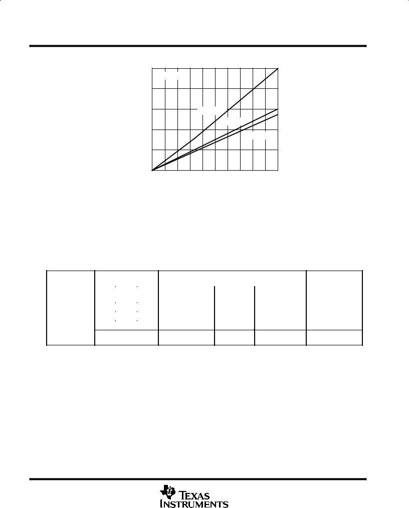
32 mV at IO = 100 mA (TPS7150) |
|
|
|
|
|||||
|
|
|
|
|
|
|
|
SENSE† /FB‡ |
|
|
EN |
|
|
2 |
7 |
|
|
||
D Very Low Quiescent Current – Independent |
|
IN |
|
|
3 |
6 |
|
|
OUT |
|
|
|
|
|
|||||
of Load . . . 285 A Typ |
|
IN |
|
|
4 |
5 |
|
|
OUT |
|
|
|
|
|
|||||
|
|
|
|
|
|||||
D Extremely Low Sleep-State Current |
|
|
|
|
|
|
|
|
|
|
|
|
|
|
|
|
|
|
|
|
|
|
|
|
|
|
|
|
|
0.5 A Max |
|
|
PW PACKAGE |
|
|||||
|
|
|
|
||||||
D2% Tolerance Over Specified Conditions For Fixed-Output Versions
DOutput Current Range of 0 mA to 500 mA
DTSSOP Package Option Offers Reduced Component Height for Space-Critical Applications
DPower-Good (PG) Status Output
description
The TPS71xx integrated circuits are a family of micropower low-dropout (LDO) voltage regulators. An order of magnitude reduction in dropout voltage and quiescent current over conventional LDO performance is achieved by replacing the typical pnp pass transistor with a PMOS device.
|
|
|
(TOP VIEW) |
|
|
||
GND |
|
|
|
PG |
|||
|
1 |
20 |
|
||||
|
|
||||||
GND |
|
2 |
19 |
|
NC |
||
|
|
||||||
GND |
|
3 |
18 |
|
NC |
||
|
|
||||||
NC |
|
4 |
17 |
|
FB‡ |
||
|
|
||||||
NC |
|
5 |
16 |
|
NC |
||
|
|
||||||
|
|
|
|
6 |
15 |
|
SENSE† |
|
EN |
|
|
|
|||
NC |
|
7 |
14 |
|
OUT |
||
|
|
||||||
|
IN |
|
8 |
13 |
|
OUT |
|
|
|
|
|||||
|
IN |
|
9 |
12 |
|
NC |
|
|
|
|
|||||
|
IN |
|
10 |
11 |
|
NC |
|
|
|
|
|||||
|
|
|
|
|
|
|
|
NC – No internal connection
† SENSE – Fixed voltage options only (TPS7133, TPS7148, and TPS7150)
‡ FB – Adjustable version only (TPS7101)
Because the PMOS device behaves as a low-value resistor, the dropout voltage is very low (maximum of 32 mV at an output current of 100 mA for the TPS7150) and is directly proportional to the output current (see Figure 1). Additionally, since the PMOS pass element is a voltage-driven device, the quiescent current is very low and remains independent of output loading (typically 285 A over the full range of output current, 0 mA to 500 mA). These two key specifications yield a significant improvement in operating life for battery-powered systems. The LDO family also features a sleep mode; applying a TTL high signal to EN (enable) shuts down the regulator, reducing the quiescent current to 0.5 A maximum at TJ = 25° C.
Please be aware that an important notice concerning availability, standard warranty, and use in critical applications of Texas Instruments semiconductor products and disclaimers thereto appears at the end of this data sheet.
PRODUCTION DATA information is current as of publication date. Products conform to specifications per the terms of Texas Instruments standard warranty. Production processing does not necessarily include testing of all parameters.
Copyright 2003, Texas Instruments Incorporated
POST OFFICE BOX 655303 • DALLAS, TEXAS 75265 |
1 |
TPS7101Q, TPS7133Q, TPS7148Q, TPS7150Q
TPS7101Y, TPS7133Y, TPS7148Y, TPS7150Y
LOW-DROPOUT VOLTAGE REGULATORS
SLVS092G – NOVEMBER 1994 – REVISED JANUARY 2003
description (continued)
|
0.25 |
|
|
|
|
|
|
|
|
|
|
|
|
TA = 25° C |
|
|
|
|
|
|
|
|
|
|
0.2 |
|
|
|
|
|
|
|
|
|
|
– V |
0.15 |
|
|
|
|
|
|
|
|
|
|
Voltage |
|
|
|
TPS7133 |
|
|
|
|
|
||
|
|
|
|
|
|
TPS7148 |
|
|
|
||
0.1 |
|
|
|
|
|
|
|
|
|
|
|
Dropout |
|
|
|
|
|
|
TPS7150 |
|
|||
|
|
|
|
|
|
|
|
||||
0.05 |
|
|
|
|
|
|
|
|
|
|
|
|
|
|
|
|
|
|
|
|
|
|
|
|
0 |
|
|
|
|
|
|
|
|
|
|
|
0 |
0.05 |
0.1 |
0.15 |
0.2 |
0.25 |
0.3 |
0.35 |
0.4 |
0.45 |
0.5 |
|
|
|
|
IO – Output Current – A |
|
|
|
||||
Figure 1. Dropout Voltage Versus Output Current
Power good (PG) reports low output voltage and can be used to implement a power-on reset or a low-battery indicator.
The TPS71xx is offered in 3.3-V, 4.85-V, and 5-V fixed-voltage versions and in an adjustable version (programmable over the range of 1.2 V to 9.75 V). Output voltage tolerance is specified as a maximum of 2% over line, load, and temperature ranges (3% for adjustable version). The TPS71xx family is available in PDIP (8 pin), SO (8 pin), and TSSOP (20-pin) packages. The TSSOP has a maximum height of 1,2 mm.
AVAILABLE OPTIONS
|
OUTPUT VOLTAGE |
PACKAGED DEVICES |
|
|
||||
|
|
(V) |
|
|
CHIP FORM |
|||
TJ |
|
|
|
|
|
|||
|
|
|
|
|
|
|||
MIN |
TYP |
MAX |
SMALL OUTLINE |
PLASTIC DIP |
TSSOP |
(Y) |
||
|
||||||||
|
(D) |
(P) |
(PW) |
|
||||
|
|
|
|
|
||||
|
|
|
|
|
|
|
|
|
|
4.9 |
5 |
5.1 |
TPS7150QD |
TPS7150QP |
TPS7150QPW |
TPS7150Y |
|
|
|
|
|
|
|
|
|
|
|
4.75 |
4.85 |
4.95 |
TPS7148QD |
TPS7148QP |
TPS7148QPW |
TPS7148Y |
|
–40° C to 125° C |
|
|
|
|
|
|
|
|
3.23 |
3.3 |
3.37 |
TPS7133QD |
TPS7133QP |
TPS7133QPW |
TPS7133Y |
||
Adjustable†
TPS7101QD TPS7101QP TPS7101QPW TPS7101Y
1.2 V to 9.75 V
† The D and PW packages are available taped and reeled. Add R suffix to device type (e.g., TPS7150QDR). The TPS7101Q is programmable using an external resistor divider (see application information). The chip form is tested at 25° C.
2 |
POST OFFICE BOX 655303 • DALLAS, TEXAS 75265 |

TPS7101Q, TPS7133Q, TPS7148Q, TPS7150Q
TPS7101Y, TPS7133Y, TPS7148Y, TPS7150Y
LOW-DROPOUT VOLTAGE REGULATORS
SLVS092G – NOVEMBER 1994 – REVISED JANUARY 2003
|
TPS71xx† |
|
|
||
VI |
8 |
|
|
20 |
PG |
IN |
|
PG |
|
||
|
9 |
SENSE |
15 |
|
|
|
IN |
|
|
||
|
10 |
|
OUT |
14 |
VO |
|
IN |
|
|
||
0.1 µ F |
6 |
|
OUT |
13 |
|
|
EN |
|
|
CO‡ |
|
|
|
|
|
+ |
|
|
|
GND |
|
10 |
µ F |
|
|
|
|
|
|
|
1 |
2 |
3 |
CSR |
|
|
|
|
|
||
† TPS7133, TPS7148, TPS7150 (fixed-voltage options)
‡Capacitor selection is nontrivial. See application information section for details.
Figure 2. Typical Application Configuration
TPS71xx chip information
These chips, when properly assembled, display characteristics similar to the TPS71xxQ. Thermal compression or ultrasonic bonding may be used on the doped aluminum bonding pads. The chips may be mounted with conductive epoxy or a gold-silicon preform.
BONDING PAD ASSIGNMENTS
|
|
|
|
|
(5) |
(4) |
|
|
|
|
|
|
(6) |
|
|
|
|
|
|
(7) |
|
|
|
|
|
|
|
|
|
|
|
80 |
|
|
|
|
|
|
|
|
|
|
|
(1) |
(2) |
|
(3) |
|
|
|
|
|
|||
|
|
|
|
|
|
|
|
|
|
|
|
|
|
|
|
|
|
|
|
|
|
92 |
|
|
|
|
|
|
|
|
|
|
|
|
|
|
|
|
|
|
|
|
|
|
(5) |
|
|
|
(3) |
|
SENSE§ |
|
IN |
|
(6) |
||
|
|
TPS71xx |
FB¶ |
||
|
|
|
(2) |
(4) |
|
|
EN |
|
|
|
OUT |
|
|
|
|
|
(7) |
|
|
|
|
|
PG |
(1) GND
CHIP THICKNESS: 15 MILS TYPICAL
BONDING PADS: 4 × 4 MILS MINIMUM
TJmax = 150° C
TOLERANCES ARE ± 10%.
ALL DIMENSIONS ARE IN MILS.
§ SENSE – Fixed voltage options only (TPS7133, TPS7148, and TPS7150)
¶ FB – Adjustable version only (TPS7101)
NOTE A: For most applications, OUT and SENSE should be tied together as close as possible to the device; for other implementations, refer to SENSE-pin connection discussion in the Applications Information section of this data sheet.
POST OFFICE BOX 655303 • DALLAS, TEXAS 75265 |
3 |

TPS7101Q, TPS7133Q, TPS7148Q, TPS7150Q
TPS7101Y, TPS7133Y, TPS7148Y, TPS7150Y
LOW-DROPOUT VOLTAGE REGULATORS
SLVS092G – NOVEMBER 1994 – REVISED JANUARY 2003
functional block diagram
IN |
|
|
|
RESISTOR DIVIDER OPTIONS |
|||
† |
† |
† |
|
DEVICE |
R1 |
R2 |
UNIT |
EN |
|
||||||
|
TPS7101 |
0 |
∞ |
Ω |
|||
|
|
|
|
||||
|
|
|
PG |
TPS7133 |
420 |
233 |
kΩ |
|
|
|
TPS7148 |
726 |
233 |
kΩ |
|
|
|
|
|
||||
_ |
|
|
|
TPS7150 |
756 |
233 |
kΩ |
+ |
|
|
|
NOTE A: Resistors are nominal values only. |
|||
|
|
OUT |
|
|
|
|
|
|
|
|
|
|
|
|
|
|
|
|
COMPONENT COUNT |
|
|
1.12 V |
SENSE‡ /FB |
MOS transistors |
464 |
|
+ |
|
Bilpolar transistors |
41 |
|
_ |
|
||
|
|
Diodes |
4 |
|
Vref = 1.178 V |
R1 |
|
||
|
|
Capacitors |
17 |
|
|
|
|
||
|
|
|
Resistors |
76 |
|
R2 |
|
|
|
GND
† Switch positions are shown with EN low (active).
‡For most applications, SENSE should be externally connected to OUT as close as possible to the device. For other implementations, refer to SENSE-pin connection discussion in Applications Information section.
absolute maximum ratings over operating free-air temperature range (unless otherwise noted)§
|
|
|
|
|
Input voltage range¶ , V , PG, SENSE, |
EN . . . . . . . . . . . . . . . . . . . . . . . . |
. . . . . . . . . . . . . . . . . . . . –0.3 V to 11 |
V |
|
I |
|
|
||
Output current, IO . . . . . . . . . . . . . . . . . . . . . . . . . . . . . . . . . . . . . . . . . . . . . |
. . . . . . . . . . . . . . . . . . . . . . . . . . . . . . 2 |
A |
||
Continuous total power dissipation . . . . . . . . . . . . . . . . . . . . . . . . . . . . . |
See Dissipation Rating Tables 1 and 2 |
|||
Operating virtual junction temperature range, TJ . . . . . . . . . . . . . . . . . . |
. . . . . . . . . . . . . . . . . . . –55° C to 150° C |
|||
Storage temperature range, Tstg . . . . . . . . . . . . . . . . . . . . . . . . . . . . . . . . |
. . . . . . . . . . . . . . . . . . . –65° C to 150° C |
|||
Lead temperature 1,6 mm (1/16 inch) from case for 10 seconds . . . . |
. . . . . . . . . . . . . . . . . . . . . . . . . . . 260° C |
|||
§Stresses beyond those listed under “absolute maximum ratings” may cause permanent damage to the device. These are stress ratings only, and functional operation of the device at these or any other conditions beyond those indicated under “recommended operating conditions” is not implied. Exposure to absolute-maximum-rated conditions for extended periods may affect device reliability.
¶ All voltage values are with respect to network terminal ground.
DISSIPATION RATING TABLE 1 – FREE-AIR TEMPERATURE (see Figure 3)#
PACKAGE |
TA ≤ 25° C |
DERATING FACTOR |
TA = 70° C |
TA = 125° C |
|
POWER RATING |
ABOVE TA = 25° C |
POWER RATING |
POWER RATING |
||
|
|||||
D |
725 mW |
5.8 mW/° C |
464 mW |
145 mW |
|
P |
1175 mW |
9.4 mW/° C |
752 mW |
235 mW |
|
PW|| |
700 mW |
5.6 mW/° C |
448 mW |
140 mW |
|
DISSIPATION RATING TABLE 2 – CASE TEMPERATURE (see Figure 4)# |
|||||
PACKAGE |
TC ≤ 25° C |
DERATING FACTOR |
TC = 70° C |
TC = 125° C |
|
POWER RATING |
ABOVE TC = 25° C |
POWER RATING |
POWER RATING |
||
|
|||||
D |
2188 mW |
17.5 mW/° C |
1400 mW |
438 mW |
|
P |
2738 mW |
21.9 mW/° C |
1752 mW |
548 mW |
|
PW|| |
4025 mW |
32.2 mW/° C |
2576 mW |
805 mW |
|
#Dissipation rating tables and figures are provided for maintenance of junction temperature at or below absolute maximum temperature of 150° C. For guidelines on maintaining junction temperature within recommended operating range, see the Thermal Information section.
|| Refer to Thermal Information section for detailed power dissipation considerations when using the TSSOP packages.
4 |
POST OFFICE BOX 655303 • DALLAS, TEXAS 75265 |

|
TPS7101Q, TPS7133Q, TPS7148Q, TPS7150Q |
|
|
TPS7101Y, TPS7133Y, TPS7148Y, TPS7150Y |
|
|
LOW-DROPOUT VOLTAGE REGULATORS |
|
|
SLVS092G – NOVEMBER 1994 – REVISED JANUARY 2003 |
|
|
|
|
DISSIPATION DERATING CURVE† |
DISSIPATION DERATING CURVE† |
|
vs
FREE-AIR TEMPERATURE
|
1400 |
|
|
|
|
|
|
– mW |
1200 |
|
|
|
|
|
|
Dissipation |
|
|
|
|
|
|
|
|
|
|
P Package |
|
|
||
1000 |
|
|
Rθ JA = 106° C/W |
|
|
||
|
|
|
|
|
|
|
|
Continuous |
800 |
|
|
|
D Package |
|
|
|
|
|
|
|
|
||
600 |
|
|
|
Rθ JA = 172° C/W |
|
||
|
|
|
|
|
|
||
|
|
|
|
|
|
|
|
– Maximum |
400 |
|
|
|
|
|
|
|
PW and PWP |
|
|
|
|||
200 |
Package |
|
|
|
|||
D |
|
R |
θ JA |
= 178° C/W |
|
|
|
P |
|
|
|
|
|
|
|
|
0 |
|
|
|
|
|
|
|
25 |
50 |
75 |
100 |
125 |
150 |
|
|
|
|
TA – Free-Air Temperature – ° C |
|
|||
|
|
|
|
vs |
|
|
|
|
|
CASE TEMPERATURE |
|
|
|
|
4800 |
|
|
|
|
|
mW |
4400 |
PW Package |
|
|
||
|
|
|
||||
– |
4000 |
|
|
|||
Rθ JC = 31° C/W |
|
|
||||
Dissipation |
|
|
||||
3600 |
|
|
|
|
|
|
3200 |
|
|
P Package |
|
|
|
|
|
Rθ JC = 46° C/W |
|
|
||
2800 |
|
|
|
|
||
Continuous |
|
|
|
|
|
|
2400 |
|
|
|
|
|
|
2000 |
|
|
|
|
|
|
1600 |
|
|
|
|
|
|
Maximum |
|
|
|
|
|
|
1200 |
|
|
|
|
|
|
800 |
|
|
|
|
|
|
– |
D Package |
|
|
|
||
|
|
|
|
|||
D |
400 |
|
|
|
||
Rθ JC = 57° C/W |
|
|
|
|||
P |
|
|
|
|||
|
|
|
|
|||
|
0 |
|
|
|
||
|
25 |
50 |
75 |
100 |
125 |
150 |
|
|
|
TC – Case Temperature – ° C |
|
||
Figure 3 |
Figure 4 |
†Dissipation rating tables and figures are provided for maintenance of junction temperature at or below absolute maximum temperature of 150° C. For guidelines on maintaining junction temperature within recommended operating range, see the Thermal Information section.
recommended operating conditions
|
|
|
|
|
|
MIN |
MAX |
UNIT |
|
|
|
|
|
|
|
|
|
|
|
|
|
|
|
|
TPS7101Q |
2.5 |
10 |
|
|
|
|
|
|
|
|
|
|
|
|
Input voltage, VI‡ |
TPS7133Q |
3.77 |
10 |
V |
|||||
|
|
|
|||||||
TPS7148Q |
5.2 |
10 |
|||||||
|
|
|
|
|
|
||||
|
|
|
|
|
|
|
|
|
|
|
|
|
|
|
TPS7150Q |
5.33 |
10 |
|
|
|
|
|
|
|
|
|
|
|
|
|
|
|
|
|
|
||||
High-level input voltage at |
EN, |
VIH |
2 |
|
V |
||||
Low-level input voltage at |
|
|
VIL |
|
0.5 |
V |
|||
EN, |
|
||||||||
Output current range, IO |
0 |
500 |
mA |
||||||
Operating virtual junction temperature range, TJ |
–40 |
125 |
° C |
||||||
‡Minimum input voltage defined in the recommended operating conditions is the maximum specified output voltage plus dropout voltage at the maximum specified load range. Since dropout voltage is a function of output current, the usable range can be extended for lighter loads. To
calculate the minimum input voltage for your maximum output current, use the following equation: VI(min) = VO(max) + VDO(max load) Becausethe TPS7101 is programmable, rDS(on) should be used to calculate VDObeforeapplyingtheaboveequation.Theequationforcalculating VDO from rDS(on) is given in Note 2 in the electrical characteristics table. The minimum value of 2.5 V is the absolute lower limit for the recommended input voltage range for the TPS7101.
POST OFFICE BOX 655303 • DALLAS, TEXAS 75265 |
5 |
TPS7101Q, TPS7133Q, TPS7148Q, TPS7150Q
TPS7101Y, TPS7133Y, TPS7148Y, TPS7150Y
LOW-DROPOUT VOLTAGE REGULATORS
SLVS092G – NOVEMBER 1994 – REVISED JANUARY 2003
electrical characteristics at IO = 10 mA, EN = 0 V, CO = 4.7 µ F/CSR† = 1 Ω , SENSE/FB shorted to OUT
(unless otherwise noted)
|
|
|
|
|
|
|
|
|
|
|
TPS7101Q, TPS7133Q |
|
||
|
|
PARAMETER |
|
|
TEST CONDITIONS‡ |
|
T |
|
|
TPS7148Q, TPS7150Q |
UNIT |
|||
|
|
|
|
|
|
|
|
J |
|
|
|
|
|
|
|
|
|
|
|
|
|
|
|
|
|
MIN |
TYP |
MAX |
|
|
|
|
|
|
|
|
|
|
|
|
|
|
|
|
|
|
|
|
|
|
|
|
25° C |
|
|
|
285 |
350 |
|
|
Ground current (active mode) |
|
EN ≤ 0.5 V, |
VI = VO + 1 V, |
|
|
|
A |
||||||
|
|
|
|
|
|
|
|
|||||||
|
0 mA ≤ IO ≤ 500 mA |
–40° C to 125° C |
|
|
460 |
|||||||||
|
|
|
|
|
|
|
|
|
||||||
|
Input current (standby mode) |
|
|
= VI, |
2.7 V ≤ VI ≤ |
10 V |
25° C |
|
|
|
|
0.5 |
A |
|
|
|
EN |
|
|
|
|
|
|
||||||
|
–40° C to 125° C |
|
|
2 |
||||||||||
|
|
|
|
|
|
|
|
|
|
|
||||
|
|
|
|
|
|
|
|
|
|
|
|
|
|
|
|
Output current limit |
|
VO = 0, |
VI = 10 V |
|
25° C |
|
|
|
1.2 |
2 |
A |
||
|
|
|
|
|
|
|
|
|
||||||
|
|
–40° C to 125° C |
|
|
2 |
|||||||||
|
|
|
|
|
|
|
|
|
|
|
||||
|
|
|
|
|
|
|
|
|
|
|
|
|
|
|
|
Pass-element leakage current in standby |
|
|
|
|
|
25° C |
|
|
|
|
0.5 |
A |
|
|
EN = VI, |
2.7 V ≤ VI ≤ |
10 V |
|
|
|
|
|||||||
|
mode |
|
° |
° |
C |
|
|
1 |
||||||
|
|
|
|
|
|
|
|
–40 C to 125 |
|
|
|
|
||
|
PG leakage current |
|
Normal operation, |
VPG = 10 V |
|
25° C |
|
|
|
0.02 |
0.5 |
A |
||
|
|
|
|
|
|
|
|
|
||||||
|
|
–40° C to 125° C |
|
|
0.5 |
|||||||||
|
|
|
|
|
|
|
|
|
|
|
||||
|
|
|
|
|
|
|
|
|
|
|
|
|
||
|
Output voltage temperature coefficient |
|
|
|
|
|
–40° C to 125° C |
|
61 |
75 |
ppm/° C |
|||
|
|
|
|
|
|
|
|
|
|
|
|
|
|
|
|
Thermal shutdown junction temperature |
|
|
|
|
|
|
|
|
|
165 |
|
° C |
|
|
|
|
|
|
|
|
|
|
|
|
|
|
|
|
|
|
|
|
2.5 V ≤ VI ≤ 6 V |
|
|
–40° C to 125° C |
2 |
|
|
V |
|||
|
EN logic high (standby mode) |
|
|
|
|
|
||||||||
|
|
6 V ≤ VI ≤ 10 V |
|
|
2.7 |
|
|
|||||||
|
|
|
|
|
|
|
|
|
|
|
|
|||
|
|
logic low (active mode) |
|
2.7 V ≤ VI ≤ 10 V |
|
|
25° C |
|
|
|
|
0.5 |
V |
|
|
EN |
|
|
|
|
|
|
|
|
|
||||
|
|
|
|
–40° C to 125° C |
|
|
0.5 |
|||||||
|
|
|
|
|
|
|
|
|
|
|
||||
|
|
|
|
|
|
|
|
|
|
|
|
|
|
|
|
|
hysteresis voltage |
|
|
|
|
|
25° C |
|
|
|
50 |
|
mV |
|
EN |
|
|
|
|
|
|
|
|
|
||||
|
|
|
|
|
|
|
|
|
|
|
|
|
|
|
|
|
input current |
|
0 V ≤ VI ≤ 10 V |
0 V ≤ VI ≤ 10 V |
25° C |
|
|
–0.5 |
|
0.5 |
A |
||
|
EN |
|
|
|
|
|
|
|
||||||
|
|
–40° C to 125° C |
–0.5 |
|
0.5 |
|||||||||
|
|
|
|
|
|
|
|
|
|
|||||
|
|
|
|
|
|
|
|
|
|
|
|
|
|
|
|
Minimum VI for active pass element |
|
|
|
|
|
25° C |
|
|
|
2.05 |
2.5 |
V |
|
|
|
|
|
|
|
|
|
|
|
|
|
|||
|
|
|
|
|
|
–40° C to 125° C |
|
|
2.5 |
|||||
|
|
|
|
|
|
|
|
|
|
|
||||
|
|
|
|
|
|
|
|
|
|
|
|
|
|
|
|
Minimum VI for valid PG |
|
IPG = 300 A |
IPG = 300 |
A |
25° C |
|
|
|
1.06 |
1.5 |
V |
||
|
|
|
|
|
|
|
|
|||||||
|
|
–40° C to 125° C |
|
|
1.9 |
|||||||||
|
|
|
|
|
|
|
|
|
|
|
||||
|
|
|
|
|
|
|
|
|
|
|
|
|
|
|
†CSR (compensation series resistance) refers to the total series resistance, including the equivalent series resistance (ESR) of the capacitor, any series resistance added externally, and PWB trace resistance to CO.
‡Pulse-testing techniques are used to maintain virtual junction temperature as close as possible to ambient temperature; thermal effects must be taken into account separately.
6 |
POST OFFICE BOX 655303 • DALLAS, TEXAS 75265 |
TPS7101Q, TPS7133Q, TPS7148Q, TPS7150Q
TPS7101Y, TPS7133Y, TPS7148Y, TPS7150Y
LOW-DROPOUT VOLTAGE REGULATORS
SLVS092G – NOVEMBER 1994 – REVISED JANUARY 2003
TPS7101 electrical characteristics at IO = 10 mA, VI = 3.5 V, EN = 0 V, CO = 4.7 µ F/CSR† = 1 Ω , FB shorted to OUT at device leads (unless otherwise noted)
PARAMETER |
|
|
TEST CONDITIONS‡ |
|
T |
|
|
TPS7101Q |
|
UNIT |
||||||
|
|
|
|
|
|
|
|
|||||||||
|
|
|
|
|
|
|
|
|||||||||
|
|
|
|
|
|
|
|
J |
|
|
MIN |
TYP |
MAX |
|
|
|
|
|
|
|
|
|
|
|
|
|
|
|
|
|
|||
Reference voltage (measured at FB |
VI = 3.5 V, |
|
IO = 10 mA |
|
25° C |
|
|
|
1.178 |
|
V |
|||||
2.5 V ≤ VI ≤ |
10 V, |
5 mA ≤ |
IO ≤ |
500 mA, |
|
|
|
|
|
|
|
|
|
|||
with OUT connected to FB) |
–40° C to 125° C |
1.143 |
|
1.213 |
V |
|||||||||||
|
See Note 1 |
|
|
|
|
|
|
|
|
|
|
|
|
|
|
|
Reference voltage temperature |
|
|
|
|
|
|
|
–40° C to 125° C |
|
61 |
75 |
ppm/° C |
||||
coefficient |
|
|
|
|
|
|
|
|
||||||||
|
|
|
|
|
|
|
|
|
|
|
|
|
|
|
|
|
|
|
|
|
|
|
|
|
|
|
|
|
|
|
|
|
|
|
VI = 2.4 V, |
|
50 |
A ≤ |
IO ≤ |
150 mA |
25° C |
|
|
|
0.7 |
1 |
|
|
|
|
|
|
|
|
|
|
|
|
|
|
|
||||||
|
|
–40° C to 125° C |
|
|
1 |
|
|
|
||||||||
|
|
|
|
|
|
|
|
|
|
|
|
|
||||
|
|
|
|
|
|
|
|
|
|
|
|
|
|
|||
|
VI = 2.4 V, |
|
150 mA ≤ IO ≤ 500 |
25° C |
|
|
|
0.83 |
1.3 |
|
|
|
||||
|
|
mA |
|
|
|
° |
° |
C |
|
|
1.3 |
|
|
|
||
Pass-element series resistance |
|
|
|
|
|
|
|
–40 C to 125 |
|
|
Ω |
|||||
|
|
|
|
|
|
|
|
|
|
|
|
|
||||
(see Note 2) |
|
|
|
|
|
|
|
° |
|
|
|
0.52 |
0.85 |
|||
|
VI = 2.9 V, |
|
50 |
A ≤ |
IO ≤ |
500 mA |
25 C |
|
|
|
|
|
|
|||
|
|
–40° C to 125° C |
|
|
0.85 |
|
|
|
||||||||
|
|
|
|
|
|
|
|
|
|
|
|
|
||||
|
|
|
|
|
|
|
|
|
|
|
|
|
|
|
|
|
|
VI = 3.9 V, |
|
50 |
A ≤ |
IO ≤ |
500 mA |
25° C |
|
|
|
0.32 |
|
|
|
|
|
|
VI = 5.9 V, |
|
50 |
A ≤ |
IO ≤ |
500 mA |
25° C |
|
|
|
0.23 |
|
|
|
|
|
Input regulation |
VI = 2.5 V to 10 V, |
50 |
A ≤ |
IO ≤ |
500 mA, |
25° C |
|
|
|
|
18 |
mV |
||||
See Note 1 |
|
|
|
|
|
° |
° |
C |
|
|
25 |
|||||
|
|
|
|
|
|
|
|
|
|
|
||||||
|
|
|
|
|
|
|
|
–40 C to 125 |
|
|
|
|
|
|
||
|
IO = 5 mA to 500 mA, |
2.5 V ≤ |
VI ≤ |
10 V, |
25° C |
|
|
|
|
14 |
mV |
|||||
|
See Note 1 |
|
|
|
|
|
° |
° |
C |
|
|
25 |
||||
|
|
|
|
|
|
|
|
|
|
|
||||||
Output regulation |
|
|
|
|
|
|
|
–40 C to 125 |
|
|
|
|
|
|
||
IO = 50 A to 500 mA, |
2.5 V ≤ |
VI ≤ |
10 V, |
25° C |
|
|
|
|
22 |
mV |
||||||
|
|
|
|
|
||||||||||||
|
See Note 1 |
|
|
|
|
|
° |
° |
C |
|
|
54 |
||||
|
|
|
|
|
|
|
|
|
|
|
||||||
|
|
|
|
|
|
|
|
–40 C to 125 |
|
|
|
|
|
|
||
|
|
|
|
IO = 50 A |
|
25° C |
|
|
48 |
59 |
|
|
|
|
||
|
|
|
|
|
|
|
|
|
|
|
|
|
|
|||
Ripple rejection |
f = 120 Hz |
|
|
–40° C to 125° C |
44 |
|
|
dB |
||||||||
|
|
|
|
|
|
|
||||||||||
|
|
|
|
|
|
|
|
|
|
|
||||||
|
IO = 500 mA, |
25° C |
|
|
45 |
54 |
|
|||||||||
|
|
|
|
|
|
|
|
|
|
|||||||
|
|
|
|
|
|
|
|
|
|
|
|
|
||||
|
|
|
|
See Note 1 |
|
° |
° |
C |
44 |
|
|
|
|
|
||
|
|
|
|
|
|
|
|
–40 C to 125 |
|
|
|
|
|
|
||
|
|
|
|
|
|
|
25° C |
|
|
|
|
|
|
|||
Output noise-spectral density |
f = 120 Hz |
|
|
|
|
|
|
|
|
2 |
|
V/√ |
Hz |
|
||
|
|
|
|
|
|
|
|
|
|
|
|
|
|
|||
|
10 Hz ≤ f ≤ |
100 kHz, |
CO = 4.7 F |
25° C |
|
|
|
95 |
|
|
|
|
||||
Output noise voltage |
CO = 10 F |
|
25° C |
|
|
|
89 |
|
Vrms |
|||||||
CSR† = 1 Ω |
|
|
|
|
|
|
||||||||||
|
|
|
|
CO = 100 F |
25° C |
|
|
|
74 |
|
|
|
|
|||
PG trip-threshold voltage§ |
VFB voltage decreasing from above VPG |
–40° C to 125° C |
1.101 |
|
1.145 |
V |
||||||||||
PG hysteresis voltage§ |
Measured at VFB |
|
|
|
|
25° C |
|
|
|
12 |
|
mV |
||||
PG output low voltage§ |
I |
= 400 A, |
V = 2.13 V |
|
25° C |
|
|
|
0.1 |
0.4 |
V |
|||||
|
|
|
|
|
|
|
||||||||||
|
|
|
|
|
|
|
||||||||||
|
PG |
|
|
I |
|
|
|
–40° C to 125° C |
|
|
0.4 |
|
|
|
||
|
|
|
|
|
|
|
|
|
|
|
|
|
||||
FB input current |
|
|
|
|
|
|
|
25° C |
|
|
–10 |
0.1 |
10 |
nA |
||
|
|
|
|
|
|
|
|
|
|
|
|
|
||||
|
|
|
|
|
|
|
–40° C to 125° C |
–20 |
|
20 |
||||||
|
|
|
|
|
|
|
|
|
|
|
|
|||||
|
|
|
|
|
|
|
|
|
|
|
|
|
|
|
|
|
†CSR refers to the total series resistance, including the ESR of the capacitor, any series resistance added externally, and PWB trace resistance to CO.
‡Pulse-testing techniques are used to maintain virtual junction temperature as close as possible to ambient temperature; thermal effects must be taken into account separately.
§ Output voltage programmed to 2.5 V with closed-loop configuration (see application information).
NOTES: 1. When VI < 2.9 V and IO > 150 mA simultaneously, pass element rDS(on) increases (see Figure 27) to a point such that the resulting dropout voltage prevents the regulator from maintaining the specified tolerance range.
2. To calculate dropout voltage, use equation:
VDO = IO rDS(on)
rDS(on) is a function of both output current and input voltage. The parametric table lists rDS(on) for VI = 2.4 V, 2.9 V, 3.9 V, and 5.9 V, which corresponds to dropout conditions for programmed output voltages of 2.5 V, 3 V, 4 V, and 6 V, respectively. For other
programmed values, refer to Figure 26.
POST OFFICE BOX 655303 • DALLAS, TEXAS 75265 |
7 |

TPS7101Q, TPS7133Q, TPS7148Q, TPS7150Q
TPS7101Y, TPS7133Y, TPS7148Y, TPS7150Y
LOW-DROPOUT VOLTAGE REGULATORS
SLVS092G – NOVEMBER 1994 – REVISED JANUARY 2003
TPS7133 electrical characteristics at I = 10 mA, V |
|
= 4.3 V, |
|
= 0 V, C |
|
= 4.7 µ F/CSR† = 1 Ω , SENSE |
|||||||||
I |
EN |
O |
|||||||||||||
|
O |
|
|
|
|
|
|
|
|
|
|
|
|
||
shorted to OUT (unless otherwise noted) |
|
|
|
|
|
|
|
|
|
|
|
|
|
|
|
|
|
|
|
|
|
|
|
|
|
|
|
|
|
|
|
PARAMETER |
TEST CONDITIONS‡ |
|
|
T |
|
|
TPS7133Q |
|
UNIT |
||||||
|
|
|
|
|
|
|
|||||||||
|
|
|
|
|
|
|
|||||||||
|
|
|
|
|
|
|
J |
|
|
MIN |
TYP |
MAX |
|
|
|
|
|
|
|
|
|
|
|
|
|
|
|
|
|||
Output voltage |
VI = 4.3 V, |
IO = 10 mA |
|
|
25° C |
|
|
3.3 |
|
V |
|||||
4.3 V ≤ VI ≤ 10 V, |
5 mA ≤ |
|
IO ≤ |
500 mA |
–40° C to 125° C |
3.23 |
|
3.37 |
|||||||
|
|
|
|
|
|
||||||||||
|
IO = 10 mA, |
VI = 3.23 V |
|
|
25° C |
|
|
4.5 |
7 |
|
|
|
|||
|
|
|
|
|
|
|
|
|
|
|
|
||||
|
|
|
–40° C to 125° C |
|
|
8 |
|
|
|
||||||
|
|
|
|
|
|
|
|
|
|
|
|
||||
|
|
|
|
|
|
|
|
|
|
|
|
|
|
|
|
Dropout voltage |
IO = 100 mA, |
VI = 3.23 V |
|
|
25° C |
|
|
47 |
60 |
mV |
|||||
|
|
|
|
|
|
|
|
||||||||
|
|
–40° C to 125° C |
|
|
80 |
||||||||||
|
|
|
|
|
|
|
|
|
|
|
|
||||
|
|
|
|
|
|
|
|
|
|
|
|
|
|
|
|
|
IO = 500 mA, |
VI = 3.23 V |
|
|
25° C |
|
|
235 |
300 |
|
|
|
|||
|
|
|
|
|
|
|
|
|
|
|
|
||||
|
|
|
–40° C to 125° C |
|
|
400 |
|
|
|
||||||
|
|
|
|
|
|
|
|
|
|
|
|
||||
|
|
|
|
|
|
|
|
|
|
|
|
|
|
|
|
Pass-element series resistance |
(3.23 V – VO)/IO, |
VI = 3.23 V, |
|
|
25° C |
|
|
0.47 |
0.6 |
Ω |
|||||
|
|
|
|
|
|
|
|
||||||||
|
|
–40° C to 125° C |
|
|
0.8 |
||||||||||
|
IO = 500 mA |
|
|
|
|
|
|
|
|
|
|
||||
Input regulation |
VI = 4.3 V to 10 V, |
50 A ≤ |
IO ≤ |
500 mA |
25° C |
|
|
|
20 |
mV |
|||||
|
|
|
|
|
|
||||||||||
–40° C to 125° C |
|
|
27 |
||||||||||||
|
|
|
|
|
|
|
|
|
|
|
|
||||
|
|
|
|
|
|
|
|
|
|
|
|
|
|
|
|
|
IO = 5 mA to 500 mA, |
4.3 V ≤ |
|
VI ≤ |
10 V |
25° C |
|
|
21 |
38 |
mV |
||||
|
|
|
|
|
|
|
|
||||||||
Output regulation |
|
–40° C to 125° C |
|
|
75 |
||||||||||
|
|
|
|
|
|
|
|
|
|
|
|||||
|
|
|
|
|
|
|
|
|
|
|
|
|
|
|
|
IO = 50 A to 500 mA, |
4.3 V ≤ |
|
VI ≤ |
10 V |
25° C |
|
|
30 |
60 |
mV |
|||||
|
|
|
|
||||||||||||
|
|
|
|
|
|
|
|
||||||||
|
|
–40° C to 125° C |
|
|
120 |
||||||||||
|
|
|
|
|
|
|
|
|
|
|
|
||||
|
|
|
|
|
|
|
|
|
|
|
|
|
|
|
|
|
|
IO = 50 A |
|
|
25° C |
|
43 |
54 |
|
|
|
|
|||
|
|
|
|
|
|
|
|
|
|
|
|
|
|||
Ripple rejection |
f = 120 Hz |
|
|
–40° C to 125° C |
40 |
|
|
dB |
|||||||
|
|
|
|
|
|
|
|||||||||
|
|
|
|
|
|
|
|
|
|
|
|||||
IO = 500 mA |
25° C |
|
39 |
49 |
|
||||||||||
|
|
|
|
|
|
|
|||||||||
|
|
|
|
|
|
|
|
|
|
|
|||||
|
|
–40° C to 125° C |
36 |
|
|
|
|
|
|||||||
|
|
|
|
|
|
|
|
|
|
|
|
||||
|
|
|
|
|
|
|
|
|
|
|
|
|
|
|
|
|
|
|
|
|
|
|
25° C |
|
|
|
|
|
|||
Output noise-spectral density |
f = 120 Hz |
|
|
|
|
|
|
|
2 |
|
V/√ |
Hz |
|
||
|
|
|
|
|
|
|
|
|
|
|
|||||
|
10 Hz ≤ f ≤ 100 kHz, |
CO = 4.7 F |
25° C |
|
|
274 |
|
|
|
|
|||||
Output noise voltage |
CO = 10 F |
|
|
25° C |
|
|
228 |
|
Vrms |
||||||
CSR† = 1 Ω |
|
|
|
|
|
||||||||||
|
|
CO = 100 F |
25° C |
|
|
159 |
|
|
|
|
|||||
PG trip-threshold voltage |
VO voltage decreasing from above VPG |
–40° C to 125° C |
2.868 |
|
3 |
V |
|||||||||
PG hysteresis voltage |
|
|
|
|
|
|
25° C |
|
|
35 |
|
mV |
|||
|
|
|
|
|
|
|
|
|
|
|
|
|
|
|
|
PG output low voltage |
IPG = 1 mA, |
VI = 2.8 V |
|
|
25° C |
|
|
0.22 |
0.4 |
V |
|||||
|
|
|
|
|
|
|
|
||||||||
|
|
–40° C to 125° C |
|
|
0.4 |
||||||||||
|
|
|
|
|
|
|
|
|
|
|
|
||||
|
|
|
|
|
|
|
|
|
|
|
|
|
|
|
|
†CSR refers to the total series resistance, including the ESR of the capacitor, any series resistance added externally, and PWB trace resistance to CO.
‡Pulse-testing techniques are used to maintain virtual junction temperature as close as possible to ambient temperature; thermal effects must be taken into account separately.
8 |
POST OFFICE BOX 655303 • DALLAS, TEXAS 75265 |
TPS7101Q, TPS7133Q, TPS7148Q, TPS7150Q
TPS7101Y, TPS7133Y, TPS7148Y, TPS7150Y
LOW-DROPOUT VOLTAGE REGULATORS
SLVS092G – NOVEMBER 1994 – REVISED JANUARY 2003
TPS7148 electrical characteristics at I |
|
= 10 mA, V = 5.85 V, |
|
|
= 0 V, C = 4.7 µ F/CSR† = 1 Ω , SENSE |
||||||||||
O |
EN |
||||||||||||||
|
|
|
I |
|
|
|
|
O |
|
|
|
|
|
|
|
shorted to OUT (unless otherwise noted) |
|
|
|
|
|
|
|
|
|
|
|
|
|||
|
|
|
|
|
|
|
|
|
|
|
|
|
|
|
|
PARAMETER |
TEST CONDITIONS‡ |
|
|
|
T |
TPS7148Q |
|
UNIT |
|||||||
|
|
|
|
|
|
||||||||||
|
|
|
|
|
|
||||||||||
|
|
|
|
|
|
|
|
|
J |
MIN |
TYP |
MAX |
|
|
|
|
|
|
|
|
|
|
|
|
|
|
|
|
|||
Output voltage |
VI = 5.85 V, |
|
|
IO = 10 mA |
|
|
|
25° C |
|
4.85 |
|
V |
|||
5.85 V ≤ VI ≤ 10 V, |
5 mA ≤ |
IO ≤ 500 mA |
–40° C to 125° C |
4.75 |
|
4.95 |
|||||||||
|
|
|
|
|
|||||||||||
|
IO = 10 mA, |
|
|
VI = 4.75 V |
|
|
|
25° C |
|
2.9 |
6 |
|
|
|
|
|
|
|
|
|
|
|
|
|
|
|
|
|
|||
|
|
|
|
|
–40° C to 125° C |
|
|
8 |
|
|
|
||||
|
|
|
|
|
|
|
|
|
|
|
|
|
|||
|
|
|
|
|
|
|
|
|
|
|
|
|
|
|
|
Dropout voltage |
IO = 100 mA, |
|
|
VI = 4.75 V |
|
|
|
25° C |
|
30 |
37 |
mV |
|||
|
|
|
|
|
|
|
|
|
|||||||
|
|
|
|
–40° C to 125° C |
|
|
54 |
||||||||
|
|
|
|
|
|
|
|
|
|
|
|
|
|||
|
|
|
|
|
|
|
|
|
|
|
|
|
|
|
|
|
IO = 500 mA, |
|
|
VI = 4.75 V |
|
|
|
25° C |
|
150 |
180 |
|
|
|
|
|
|
|
|
|
|
|
|
|
|
|
|
|
|||
|
|
|
|
|
–40° C to 125° C |
|
|
250 |
|
|
|
||||
|
|
|
|
|
|
|
|
|
|
|
|
|
|||
|
|
|
|
|
|
|
|
|
|
|
|
|
|
|
|
Pass-element series resistance |
(4.75 V – VO)/IO, |
VI = 4.75 V, |
|
|
|
25° C |
|
0.32 |
0.35 |
Ω |
|||||
|
|
|
|
|
|
|
|||||||||
|
|
–40° C to 125° C |
|
|
0.52 |
||||||||||
|
IO = 500 mA |
|
|
|
|
|
|
|
|
|
|
|
|||
Input regulation |
VI = 5.85 V to 10 V, |
50 A ≤ |
IO ≤ |
500 mA |
|
25° C |
|
|
27 |
mV |
|||||
|
|
|
|
|
|||||||||||
–40° C to 125° C |
|
|
37 |
||||||||||||
|
|
|
|
|
|
|
|
|
|
|
|
|
|||
|
|
|
|
|
|
|
|
|
|
|
|
|
|
|
|
|
IO = 5 mA to 500 mA, |
5.85 V ≤ |
VI ≤ |
10 V |
|
25° C |
|
12 |
42 |
mV |
|||||
|
|
|
|
|
|
||||||||||
Output regulation |
–40° C to 125° C |
|
|
80 |
|||||||||||
|
|
|
|
|
|
|
|
|
|
|
|
||||
|
|
|
|
|
|
|
|
|
|
|
|
|
|
|
|
IO = 50 A to 500 mA, |
5.85 V ≤ |
VI ≤ |
10 V |
|
25° C |
|
42 |
60 |
mV |
||||||
|
|
|
|||||||||||||
|
|
|
|
|
|
||||||||||
|
–40° C to 125° C |
|
|
130 |
|||||||||||
|
|
|
|
|
|
|
|
|
|
|
|
|
|||
|
|
|
|
|
|
|
|
|
|
|
|
|
|
|
|
|
|
|
|
IO = 50 A |
|
|
|
25° C |
42 |
53 |
|
|
|
|
|
|
|
|
|
|
|
|
|
|
|
|
|
|
|
||
Ripple rejection |
f = 120 Hz |
|
|
|
|
–40° C to 125° C |
39 |
|
|
dB |
|||||
|
|
|
|
|
|
|
|
||||||||
|
|
|
|
|
|
|
|
|
|
|
|||||
|
|
IO = 500 mA |
|
|
|
25° C |
39 |
50 |
|
||||||
|
|
|
|
|
|
|
|
|
|
|
|||||
|
|
|
|
|
|
|
|
|
|
|
|
|
|
||
|
|
|
|
|
|
–40° C to 125° C |
35 |
|
|
|
|
|
|||
|
|
|
|
|
|
|
|
|
|
|
|
|
|||
|
|
|
|
|
|
|
|
|
|
|
|
|
|
|
|
|
|
|
|
|
|
|
|
|
|
|
|
|
|
||
Output noise-spectral density |
f = 120 Hz |
|
|
|
|
|
|
|
25° C |
|
2 |
|
V/√ |
Hz |
|
|
|
|
|
|
|
|
|
|
|
|
|
|
|
|
|
|
10 Hz ≤ f ≤ 100 kHz, |
CO = 4.7 F |
|
|
|
25° C |
|
410 |
|
|
|
|
|||
Output noise voltage |
CO = 10 F |
|
|
|
25° C |
|
328 |
|
Vrms |
||||||
CSR† = 1 Ω |
|
|
|
|
|
|
|
||||||||
|
|
|
|
CO = 100 F |
|
|
|
25° C |
|
212 |
|
|
|
|
|
PG trip-threshold voltage |
VO voltage decreasing from above VPG |
–40° C to 125° C |
4.5 |
|
4.7 |
V |
|||||||||
PG hysteresis voltage |
|
|
|
|
|
|
|
|
25° C |
|
50 |
|
mV |
||
|
|
|
|
|
|
|
|
|
|
|
|
|
|
|
|
PG output low voltage |
IPG = 1.2 mA, |
|
VI = 4.12 V |
|
|
|
25° C |
|
0.2 |
0.4 |
V |
||||
|
|
|
|
|
|
|
|
||||||||
|
|
|
–40° C to 125° C |
|
|
0.4 |
|||||||||
|
|
|
|
|
|
|
|
|
|
|
|
|
|||
†CSR refers to the total series resistance, including the ESR of the capacitor, any series resistance added externally, and PWB trace resistance to CO.
‡Pulse-testing techniques are used to maintain virtual junction temperature as close as possible to ambient temperature; thermal effects must be taken into account separately.
POST OFFICE BOX 655303 • DALLAS, TEXAS 75265 |
9 |
TPS7101Q, TPS7133Q, TPS7148Q, TPS7150Q
TPS7101Y, TPS7133Y, TPS7148Y, TPS7150Y
LOW-DROPOUT VOLTAGE REGULATORS
SLVS092G – NOVEMBER 1994 – REVISED JANUARY 2003
TPS7150 electrical characteristics at IO = 10 mA, VI = 6 V, EN = 0 V, CO = 4.7 µ F/CSR† = 1 Ω , SENSE shorted to OUT (unless otherwise noted)
PARAMETER |
TEST CONDITIONS‡ |
|
|
T |
TPS7150Q |
|
UNIT |
|||||
|
|
|
|
|
||||||||
|
|
|
|
|
||||||||
|
|
|
|
|
|
J |
MIN |
TYP |
MAX |
|
|
|
|
|
|
|
|
|
|
|
|
|
|||
Output voltage |
VI = 6 V, |
IO = 10 mA |
|
25° C |
|
5 |
|
V |
||||
6 V ≤ VI ≤ 10 V, |
5 mA ≤ IO ≤ |
500 mA |
–40° C to 125° C |
4.9 |
|
5.1 |
||||||
|
|
|
|
|
||||||||
|
IO = 10 mA, |
VI = 4.88 V |
|
25° C |
|
2.9 |
6 |
|
|
|
||
|
|
|
|
|
|
|
|
|
||||
|
|
–40° C to 125° C |
|
|
8 |
|
|
|
||||
|
|
|
|
|
|
|
|
|
|
|
||
|
|
|
|
|
|
|
|
|
|
|
|
|
Dropout voltage |
IO = 100 mA, |
VI = 4.88 V |
|
25° C |
|
27 |
32 |
mV |
||||
|
|
|
|
|
||||||||
|
–40° C to 125° C |
|
|
47 |
||||||||
|
|
|
|
|
|
|
|
|
|
|
||
|
|
|
|
|
|
|
|
|
|
|
|
|
|
IO = 500 mA, |
VI = 4.88 V |
|
25° C |
|
146 |
170 |
|
|
|
||
|
|
|
|
|
|
|
|
|
||||
|
|
–40° C to 125° C |
|
|
230 |
|
|
|
||||
|
|
|
|
|
|
|
|
|
|
|
||
|
|
|
|
|
|
|
|
|
|
|
|
|
Pass-element series resistance |
(4.88 V – VO)/IO, |
VI = 4.88 V, |
|
25° C |
|
0.29 |
0.32 |
Ω |
||||
|
|
|
|
|
||||||||
|
–40° C to 125° C |
|
|
0.47 |
||||||||
|
IO = 500 mA |
|
|
|
|
|
|
|
|
|
||
Input regulation |
VI = 6 V to 10 V, |
50 A ≤ IO ≤ |
500 mA |
25° C |
|
|
25 |
mV |
||||
|
|
|
|
|||||||||
–40° C to 125° C |
|
|
32 |
|||||||||
|
|
|
|
|
|
|
|
|
|
|
||
|
|
|
|
|
|
|
|
|
|
|
|
|
|
IO = 5 mA to 500 mA, |
6 V ≤ |
VI ≤ |
10 V |
25° C |
|
30 |
45 |
mV |
|||
|
|
|
|
|
||||||||
Output regulation |
–40° C to 125° C |
|
|
86 |
||||||||
|
|
|
|
|
|
|
|
|
|
|||
|
|
|
|
|
|
|
|
|
|
|
|
|
IO = 50 A to 500 mA, |
6 V ≤ |
VI ≤ |
10 V |
25° C |
|
45 |
65 |
mV |
||||
|
|
|||||||||||
|
|
|
|
|
||||||||
|
–40° C to 125° C |
|
|
140 |
||||||||
|
|
|
|
|
|
|
|
|
|
|
||
|
|
|
|
|
|
|
|
|
|
|
|
|
|
|
IO = 50 A |
|
25° C |
45 |
55 |
|
|
|
|
||
|
|
|
|
|
|
|
|
|
|
|||
Ripple rejection |
f = 120 Hz |
|
–40° C to 125° C |
40 |
|
|
dB |
|||||
|
|
|
|
|
|
|||||||
|
|
|
|
|
|
|
|
|||||
IO = 500 mA |
25° C |
42 |
52 |
|
||||||||
|
|
|
|
|
|
|||||||
|
|
|
|
|
|
|
|
|
||||
|
|
–40° C to 125° C |
36 |
|
|
|
|
|
||||
|
|
|
|
|
|
|
|
|
|
|
||
|
|
|
|
|
|
|
|
|
|
|
|
|
|
|
|
|
|
|
25° C |
|
|
|
|
||
Output noise-spectral density |
f = 120 Hz |
|
|
|
|
|
2 |
|
V/√ |
Hz |
|
|
|
|
|
|
|
|
|
|
|
|
|
||
|
10 Hz ≤ f ≤ 100 kHz, |
CO = 4.7 F |
|
25° C |
|
430 |
|
|
|
|
||
Output noise voltage |
CO = 10 F |
|
25° C |
|
345 |
|
Vrms |
|||||
CSR† = 1 Ω |
|
|
|
|||||||||
|
|
CO = 100 F |
25° C |
|
220 |
|
|
|
|
|||
PG trip-threshold voltage |
VO voltage decreasing from above VPG |
–40° C to 125° C |
4.55 |
|
4.75 |
V |
||||||
PG hysteresis voltage |
|
|
|
|
|
25° C |
|
53 |
|
mV |
||
|
|
|
|
|
|
|
|
|
|
|
|
|
PG output low voltage |
IPG = 1.2 mA, |
VI = 4.25 V |
|
25° C |
|
0.2 |
0.4 |
V |
||||
|
|
|
|
|
||||||||
|
–40° C to 125° C |
|
|
0.4 |
||||||||
|
|
|
|
|
|
|
|
|
|
|
||
|
|
|
|
|
|
|
|
|
|
|
|
|
†CSR refers to the total series resistance, including the ESR of the capacitor, any series resistance added externally, and PWB trace resistance to CO.
‡Pulse-testing techniques are used to maintain virtual junction temperature as close as possible to ambient temperature; thermal effects must be taken into account separately.
10 |
POST OFFICE BOX 655303 • DALLAS, TEXAS 75265 |
TPS7101Q, TPS7133Q, TPS7148Q, TPS7150Q
TPS7101Y, TPS7133Y, TPS7148Y, TPS7150Y
LOW-DROPOUT VOLTAGE REGULATORS
SLVS092G – NOVEMBER 1994 – REVISED JANUARY 2003
electrical characteristics at IO = 10 mA, |
|
|
|
|
= 0 V, CO = 4.7 µ F/CSR† = 1 Ω |
, TJ = 25° C, SENSE/FB |
|||||||||||||||||
EN |
|||||||||||||||||||||||
shorted to OUT (unless otherwise noted) |
|
|
|
|
|
|
|
|
|
|
|
|
|
|
|
||||||||
|
|
|
|
|
|
|
|
|
|
|
|
|
|
|
|
|
|
|
|
|
|
||
|
|
|
|
|
|
|
|
|
|
|
|
|
|
|
|
|
|
TPS7101Y, TPS7133Y |
|
|
|
||
|
|
PARAMETER |
|
|
|
|
|
|
TEST CONDITIONS‡ |
|
|
|
|
TPS7148Y, TPS7150Y |
UNIT |
||||||||
|
|
|
|
|
|
|
|
|
|
|
|
|
|
|
|
|
|
MIN |
TYP |
MAX |
|
|
|
|
|
|
|
|
|
|
|
|
|
|
|
|
|
|
|
||||||||
|
|
|
|
|
|
|
|
≤ 0.5 V, |
VI = VO + 1 V, |
|
|
|
|
|
|
|
|
||||||
|
Ground current (active mode) |
|
|
|
EN |
|
|
|
285 |
|
µ A |
||||||||||||
|
|
|
|
|
0 mA ≤ IO ≤ 500 mA |
|
|
|
|
|
|
|
|
|
|
|
|
|
|||||
|
Output current limit |
|
|
VO = 0, |
|
|
VI = 10 V |
|
|
|
|
|
1.2 |
|
A |
||||||||
|
PG leakage current |
|
|
Normal operation, |
VPG = 10 V |
|
|
|
|
0.02 |
|
µ A |
|||||||||||
|
Thermal shutdown junction temperature |
|
|
|
|
|
|
|
|
|
|
|
|
|
|
|
|
165 |
|
° C |
|||
|
|
|
|
|
|
|
|
|
|
|
|
|
|
|
|
|
|
|
|
|
|
|
|
|
|
hysteresis voltage |
|
|
|
|
|
|
|
|
|
|
|
|
|
|
|
|
50 |
|
mV |
||
|
EN |
|
|
|
|
|
|
|
|
|
|
|
|
|
|
|
|
|
|||||
|
|
|
|
|
|
|
|
|
|
|
|
|
|
|
|
|
|
|
|
|
|
|
|
|
Minimum VI for active pass element |
|
|
|
|
|
|
|
|
|
|
|
|
|
|
|
|
2.05 |
|
V |
|||
|
Minimum VI for valid PG |
|
|
IPG = 300 µ A |
|
|
|
|
|
|
|
|
1.06 |
|
V |
||||||||
|
|
|
|
|
|
|
|
|
|
|
|
|
|
|
|
|
|
|
|
|
|
|
|
|
|
PARAMETER |
|
|
|
|
|
|
TEST CONDITIONS‡ |
|
|
|
|
TPS7101Y |
|
UNIT |
|||||||
|
|
|
|
|
|
|
|
|
|
|
|
|
|
|
|||||||||
|
|
|
|
|
|
|
|
|
|
|
|
MIN |
TYP |
MAX |
|||||||||
|
|
|
|
|
|
|
|
|
|
|
|
|
|
|
|
|
|
|
|
|
|||
|
|
|
|
|
|
|
|
|
|
|
|
|
|
|
|
|
|
|
|
|
|
|
|
|
Reference voltage (measured at FB with OUT |
VI = 3.5 V, |
|
|
IO = 10 mA |
|
|
|
|
|
1.178 |
|
V |
||||||||||
|
connected to FB) |
|
|
|
|
|
|
|
|
||||||||||||||
|
|
|
|
|
|
|
|
|
|
|
|
|
|
|
|
|
|
|
|
|
|
||
|
|
|
|
|
|
|
|
|
|
|
|
|
|
|
|
|
|||||||
|
|
|
VI = 2.4 V, |
|
|
50 µ |
A ≤ |
IO ≤ |
150 mA |
|
|
0.7 |
|
|
|
|
|||||||
|
|
|
VI = 2.4 V, |
|
|
150 mA ≤ IO ≤ 500 mA |
|
|
0.83 |
|
|
|
|
||||||||||
|
Pass-element series resistance (see Note 2) |
VI = 2.9 V, |
|
|
50 µ |
A ≤ |
IO ≤ |
500 mA |
|
|
0.52 |
|
Ω |
||||||||||
|
|
|
VI = 3.9 V, |
|
|
50 µ |
A ≤ |
IO ≤ |
500 mA |
|
|
0.32 |
|
|
|
|
|||||||
|
|
|
VI = 5.9 V, |
|
|
50 µ |
A ≤ |
IO ≤ |
500 mA |
|
|
0.23 |
|
|
|
|
|||||||
|
Input regulation |
VI = 2.5 V to 10 V, |
50 µ |
A ≤ |
IO ≤ |
500 mA, |
|
|
|
18 |
mV |
||||||||||||
|
See Note 1 |
|
|
|
|
|
|
|
|
|
|
|
|||||||||||
|
|
|
|
|
|
|
|
|
|
|
|
|
|
|
|
|
|
||||||
|
|
|
|
|
|
|
|
|
|
|
|
|
|
||||||||||
|
|
|
2.5 V ≤ VI ≤ |
10 V, |
IO = 5 mA to 500 mA, |
|
|
|
14 |
mV |
|||||||||||||
|
|
|
See Note 1 |
|
|
|
|
|
|
|
|
|
|
|
|||||||||
|
Output regulation |
|
|
|
|
|
|
|
|
|
|
|
|
|
|
|
|||||||
|
|
|
|
|
|
|
|
|
|
|
|
|
|
|
|
|
|
|
|
|
|
||
|
2.5 V ≤ VI ≤ |
10 V, |
IO = 50 µ A to 500 mA, |
|
|
|
22 |
mV |
|||||||||||||||
|
|
|
|
|
|
||||||||||||||||||
|
|
|
See Note 1 |
|
|
|
|
|
|
|
|
|
|
|
|||||||||
|
|
|
|
|
|
|
|
|
|
|
|
|
|
|
|
|
|
||||||
|
|
|
|
|
|
|
|
|
|
|
|
|
|
|
|
|
|||||||
|
Ripple rejection |
VI = 3.5 V, |
|
|
f = 120 Hz, |
|
|
|
|
|
59 |
|
dB |
||||||||||
|
IO = 50 µ A |
|
|
|
|
|
|
|
|
|
|
|
|||||||||||
|
|
|
|
|
|
|
|
|
|
|
|
|
|
|
|
|
|
||||||
|
|
|
|
|
|
|
|
|
|
|
|
|
|
||||||||||
|
Output noise-spectral density |
VI = 3.5 V, |
|
|
f = 120 Hz |
|
|
|
|
|
2 |
|
µ V/√ |
Hz |
|
||||||||
|
|
|
VI = 3.5 V, |
|
|
CO = 4.7 µ F |
|
|
|
|
95 |
|
|
|
|
||||||||
|
|
|
|
|
CO = 10 µ F |
|
|
|
|
|
|
|
µ Vrms |
||||||||||
|
Output noise voltage |
10 Hz ≤ f ≤ |
100 kHz, |
|
|
|
|
|
|
89 |
|
||||||||||||
|
|
|
CSR† = 1 Ω |
|
|
|
|
|
|
|
|
|
|
|
|
|
|
|
|||||
|
|
|
|
|
CO = 100 µ F |
|
|
|
|
74 |
|
|
|
|
|||||||||
|
|
|
|
|
|
|
|
|
|
|
|
|
|
|
|
|
|
|
|||||
|
PG hysteresis voltage§ |
V = 3.5 V, |
|
|
Measured at V |
FB |
|
|
12 |
|
mV |
||||||||||||
|
|
|
|
|
I |
|
|
|
|
|
|
|
|
|
|
|
|
|
|||||
|
PG output low voltage§ |
V = 2.13 V, |
I |
= 400 µ |
A |
|
|
|
|
0.1 |
|
V |
|||||||||||
|
|
|
|
|
I |
|
|
PG |
|
|
|
|
|
|
|
|
|
|
|
|
|||
|
FB input current |
VI = 3.5 V |
|
|
VI = 3.5 V |
|
|
|
|
|
0.1 |
|
nA |
||||||||||
†CSR refers to the total series resistance, including the ESR of the capacitor, any series resistance added externally, and PWB trace resistance to CO.
‡Pulse-testing techniques are used to maintain virtual junction temperature as close as possible to ambient temperature; thermal effects must be taken into account separately.
§ Output voltage programmed to 2.5 V with closed-loop configuration (see application information).
NOTES: 1. When VI < 2.9 V and IO > 150 mA simultaneously, pass element rDS(on) increases (see Figure 27) to a point such that the resulting dropout voltage prevents the regulator from maintaining the specified tolerance range.
2. To calculate dropout voltage, use equation:
VDO = IO rDS(on)
rDS(on) is a function of both output current and input voltage. The parametric table lists rDS(on) for VI = 2.4 V, 2.9 V, 3.9 V, and 5.9 V, which corresponds to dropout conditions for programmed output voltages of 2.5 V, 3 V, 4 V, and 6 V, respectively. For other
programmed values, refer to Figure 26.
POST OFFICE BOX 655303 • DALLAS, TEXAS 75265 |
11 |

TPS7101Q, TPS7133Q, TPS7148Q, TPS7150Q
TPS7101Y, TPS7133Y, TPS7148Y, TPS7150Y
LOW-DROPOUT VOLTAGE REGULATORS
SLVS092G – NOVEMBER 1994 – REVISED JANUARY 2003
electrical characteristics at IO = 10 mA, EN = 0 V, CO = 4.7 µ F/CSR† = 1 Ω , TJ = 25° C, SENSE shorted to OUT (unless otherwise noted) (continued)
PARAMETER |
|
|
TEST CONDITIONS‡ |
TPS7133Y |
|
UNIT |
||||
|
|
|
|
|
||||||
|
|
MIN |
TYP |
MAX |
||||||
|
|
|
|
|
|
|
|
|||
|
|
|
|
|
|
|
|
|
|
|
Output voltage |
VI = 4.3 V, |
|
IO = 10 mA |
|
3.3 |
|
V |
|||
|
VI = 3.23 V, |
IO = 10 mA |
|
0.02 |
|
|
|
|
||
Dropout voltage |
VI = 3.23 V, |
IO = 100 mA |
|
47 |
|
mV |
||||
|
VI = 3.23 V, |
IO = 500 mA |
|
235 |
|
|
|
|
||
Pass-element series resistance |
(3.23 V – VO)/IO, |
VI = 3.23 V, |
|
0.47 |
|
Ω |
||||
IO = 500 mA |
|
|
|
|||||||
|
|
|
|
|
|
|
|
|||
Output regulation |
4.3 V ≤ |
VI ≤ |
10 V, |
IO = 5 mA to 500 mA |
|
21 |
|
mV |
||
4.3 V ≤ |
VI ≤ |
10 V, |
IO = 50 µ A to 500 mA |
|
30 |
|
mV |
|||
|
|
|
||||||||
Ripple rejection |
VI = 4.3 V, |
|
IO = 50 µ A |
|
54 |
|
dB |
|||
f = 120 Hz |
|
IO = 500 mA |
|
49 |
|
|||||
|
|
|
|
|
|
|
||||
|
|
|
|
|
|
|
|
|||
Output noise-spectral density |
VI = 4.3 V, |
|
f = 120 Hz |
|
2 |
|
µ V/√ |
Hz |
|
|
|
VI = 4.3 V, |
|
CO = 4.7 µ F |
|
274 |
|
|
|
|
|
Output noise voltage |
10 Hz ≤ |
f ≤ |
100 kHz, |
CO = 10 µ F |
|
228 |
|
µ Vrms |
||
|
CSR† = 1 Ω |
|
|
|
|
|
|
|
|
|
|
|
CO = 100 µ F |
|
159 |
|
|
|
|
||
|
|
|
|
|
|
|
|
|
||
PG hysteresis voltage |
VI = 4.3 V |
|
|
|
35 |
|
mV |
|||
PG output low voltage |
VI = 2.8 V, |
|
IPG = 1 mA |
|
0.22 |
|
V |
|||
PARAMETER |
|
|
TEST CONDITIONS‡ |
TPS7148Y |
|
UNIT |
||||
|
|
|
|
|
||||||
|
|
MIN |
TYP |
MAX |
||||||
|
|
|
|
|
|
|
|
|||
|
|
|
|
|
|
|
|
|
|
|
Output voltage |
VI = 5.85 V, |
|
IO = 10 mA |
|
4.85 |
|
V |
|||
|
VI = 4.75 V, |
|
IO = 10 mA |
|
0.08 |
|
|
|
|
|
Dropout voltage |
VI = 4.75 V, |
|
IO = 100 mA |
|
30 |
|
mV |
|||
|
VI = 4.75 V, |
|
IO = 500 mA |
|
150 |
|
|
|
|
|
Pass-element series resistance |
(4.75 V – VO)/IO, |
VI = 4.75 V, |
|
0.32 |
|
Ω |
||||
IO = 500 mA |
|
|
|
|||||||
|
|
|
|
|
|
|
|
|||
Output regulation |
5.85 V ≤ |
VI ≤ |
10 V, |
IO = 5 mA to 500 mA |
|
12 |
|
mV |
||
5.85 V ≤ |
VI ≤ |
10 V, |
IO = 50 µ A to 500 mA |
|
42 |
|
mV |
|||
|
|
|
||||||||
Ripple rejection |
VI = 5.85 V, |
|
IO = 50 µ A |
|
53 |
|
dB |
|||
f = 120 Hz |
|
IO = 500 mA |
|
50 |
|
|||||
|
|
|
|
|
|
|
||||
|
|
|
|
|
|
|
|
|||
Output noise-spectral density |
VI = 5.85 V, |
|
f = 120 Hz |
|
2 |
|
µ V/√ |
Hz |
|
|
|
VI = 5.85 V, |
|
CO = 4.7 µ F |
|
410 |
|
|
|
|
|
Output noise voltage |
10 Hz ≤ |
f ≤ 100 kHz, |
CO = 10 µ F |
|
328 |
|
µ Vrms |
|||
|
CSR† = 1 Ω |
|
|
|
|
|
|
|
|
|
|
|
CO = 100 µ F |
|
212 |
|
|
|
|
||
|
|
|
|
|
|
|
|
|
||
PG hysteresis voltage |
VI = 5.85 V |
|
|
|
50 |
|
mV |
|||
PG output low voltage |
VI = 4.12 V, |
|
IPG = 1.2 mA |
|
0.2 |
0.4 |
V |
|||
†CSR refers to the total series resistance, including the ESR of the capacitor, any series resistance added externally, and PWB trace resistance to CO.
‡Pulse-testing techniques are used to maintain virtual junction temperature as close as possible to ambient temperature; thermal effects must be taken into account separately.
12 |
POST OFFICE BOX 655303 • DALLAS, TEXAS 75265 |
Loading...