


TEXAS INSTRUMENTS TPS2041A, TPS2042A, TPS2043A, TPS2044A, TPS2051A Technical data
...TPS2041A, TPS2042A, TPS2043A, TPS2044A
TPS2051A, TPS2052A, TPS2053A, TPS2054A
CURRENT-LIMITED POWER-DISTRIBUTION SWITCHES
SLVS247 ± SEPTEMBER 2000
D 80-mΩ High-Side MOSFET Switch |
|
|
TPS2041A, TPS2051A |
|
|
TPS2042A, TPS2052A |
||||||||||||||||||
D 500 mA Continuous Current Per Channel |
|
|
|
|
|
D PACKAGE |
|
|
|
|
|
|
|
|
D PACKAGE |
|
|
|
|
|||||
|
|
|
|
|
|
(TOP VIEW) |
|
|
|
|
|
|
|
|
(TOP VIEW) |
|
|
|
|
|||||
D Independent Thermal and Short-Circuit |
|
|
|
|
|
|
|
|
|
|
|
|
|
|
|
|
|
|
|
|
|
|
|
|
|
|
|
|
|
|
|
|
|
|
|
|
|
|
|
|
|
|
|
|
|
|
|
||
|
Protection With Overcurrent Logic Output |
GND |
|
1 |
8 |
OUT |
|
|
GND |
1 |
8 |
OC1 |
||||||||||||
D Operating Range . . . 2.7 V to 5.5 V |
|
|
IN |
|
2 |
7 |
OUT |
|
|
IN |
2 |
7 |
OUT1 |
|||||||||||
|
|
|
|
|
|
|
|
|
|
|
|
|
|
|
|
|
|
|
|
|
|
|
||
|
|
IN |
|
3 |
6 |
OUT |
|
|
EN1² |
3 |
6 |
OUT2 |
||||||||||||
D CMOSand TTL-Compatible Enable Inputs |
|
|
|
|
|
|||||||||||||||||||
|
|
|
² |
|
|
|
|
|
|
|
|
|
|
|
EN2 |
² |
4 |
5 |
|
OC2 |
|
|||
|
EN |
|
4 |
5 |
OC |
|
|
|
|
|
|
|||||||||||||
D 2.5-ms Typical Rise Time |
|
|
|
|
|
|
|
|
|
|
|
|
|
|
|
|
|
|
|
|
|
|
|
|
|
|
|
|
|
|
|
|
|
|
|
|
|
|
|
|
|
|
|
|
|
|
|
||
|
|
|
|
|
|
|
|
|
|
|
|
|
|
|
|
|
|
|
|
|
|
|
||
D |
Undervoltage Lockout |
|
|
|
TPS2043A, TPS2053A |
|
|
TPS2044A, TPS2054A |
||||||||||||||||
|
|
|
|
|
|
|
||||||||||||||||||
D 10 µA Maximum Standby Supply Current |
|
|
|
|
|
|
|
D PACKAGE |
|
|
|
|
D PACKAGE |
|
|
|
|
|||||||
|
for Single and Dual (20 µA for Triple and |
|
|
|
|
|
|
|
(TOP VIEW) |
|
|
|
|
(TOP VIEW) |
|
|
|
|
||||||
|
|
|
|
|
|
|
|
|
|
|
|
|
|
|
|
|
|
|
|
|
|
|
|
|
|
Quad) |
GNDA |
|
|
|
|
|
|
GNDA |
|
|
|
||||||||||||
|
|
1 |
16 |
|
OC1 |
|
1 |
16 |
OC1 |
|
||||||||||||||
|
|
|
|
|||||||||||||||||||||
D |
Bidirectional Switch |
|
|
IN1 |
|
2 |
15 |
|
OUT1 |
|
|
IN1 |
2 |
15 |
OUT1 |
|||||||||
|
|
|
|
|||||||||||||||||||||
D Ambient Temperature Range, 0°C to 85°C |
|
|
EN1 |
² |
|
3 |
14 |
|
OUT2 |
|
|
EN1 |
² |
3 |
14 |
OUT2 |
||||||||
|
|
|
|
|||||||||||||||||||||
D |
ESD Protection |
|
|
EN2 |
² |
|
4 |
13 |
|
OC2 |
|
|
EN2 |
² |
4 |
13 |
OC2 |
|
||||||
|
|
|
|
|
||||||||||||||||||||
GNDB |
|
5 |
12 |
|
OC3 |
GNDB |
5 |
12 |
OC3 |
|||||||||||||||
D UL Listed ± File No. E169910 |
|
|
||||||||||||||||||||||
|
|
IN2 |
|
6 |
11 |
|
OUT3 |
|
|
IN2 |
6 |
11 |
OUT3 |
|||||||||||
|
|
|
|
|
|
|||||||||||||||||||
|
|
|
|
|
|
|
|
|||||||||||||||||
description |
|
|
EN3 |
² |
|
7 |
10 |
|
NC |
|
|
EN3 |
² |
7 |
10 |
OUT4 |
||||||||
|
|
|
|
|||||||||||||||||||||
|
|
|
|
|
|
|
|
|
|
|
|
|
|
|
|
|
|
|
|
|
|
|
||
|
|
NC |
|
8 |
9 |
|
NC |
|
EN4² |
8 |
9 |
OC4 |
||||||||||||
|
|
|
|
|
|
|
||||||||||||||||||
|
The TPS2041A through TPS2044A and |
|
|
|
|
|
|
|
|
|
|
|
|
|
|
|
|
|
|
|
|
|
|
|
|
² All enable inputs are active high for the TPS205xA series. |
|||||||||||||||||||||||
|
TPS2051A through TPS2054A power-distribution |
|||||||||||||||||||||||
switches are intended for applications where |
NC ± No connect |
|
heavy capacitive loads and short circuits are likely to be encountered. These devices incorporate 80-mΩ N-channel MOSFET high-side power switches for power-distribution systems that require multiple power switches in a single package. Each switch is controlled by an independent logic enable input. Gate drive is provided by an internal charge pump designed to control the power-switch rise times and fall times to minimize current surges during switching. The charge pump requires no external components and allows operation from supplies as low as 2.7 V.
When the output load exceeds the current-limit threshold or a short is present, these devices limit the output current to a safe level by switching into a constant-current mode, pulling the overcurrent (OCx) logic output low. When continuous heavy overloads and short circuits increase the power dissipation in the switch, causing the junction temperature to rise, a thermal protection circuit shuts off the switch to prevent damage. Recovery from a thermal shutdown is automatic once the device has cooled sufficiently. Internal circuitry ensures the switch remains off until valid input voltage is present. These power-distribution switches are designed to current limit at 0.9 A.
GENERAL SWITCH CATALOG
33 mΩ, single |
TPS201xA |
0.2 A ± 2 A |
|
80 mΩ, dual |
TPS2042 |
500 mA |
80 mΩ, dual |
80 mΩ, triple |
80 mΩ, quad |
80 mΩ, quad |
||||
|
TPS202x |
0.2 A ± 2 A |
|
|
TPS2052 |
500 mA |
|
|
|
|
|
|
|
|
|
TPS203x |
0.2 A ± 2 A |
|
|
TPS2046 |
250 mA |
|
|
|
|
|
|
|
|
|
|
|
|
|
TPS2056 |
250 mA |
|
|
|
|
|
|
|
|
80 mΩ, single |
TPS2014 |
600 mA |
|
260 mΩ |
TPS2100/1 |
|
TPS2080 |
500 mA |
|
|
|
|
|
|
|
TPS2015 |
1 A |
IN1 |
|
IN1 |
500 mA |
TPS2081 |
500 mA |
TPS2043 |
500 mA |
|
|
|
|
|
TPS2041 |
500 mA |
|
IN2 |
10 mA |
TPS2082 |
500 mA |
TPS2053 |
500 mA |
TPS2044 |
500 mA |
TPS2085 |
500 mA |
|
|
IN2 |
OUT |
||||||||||||
|
TPS2051 |
500 mA |
TPS2102/3/4/5 |
TPS2090 |
250 mA |
TPS2047 |
250 mA |
TPS2086 |
500 mA |
|||||
|
|
TPS2054 |
500 mA |
|||||||||||
|
TPS2045 |
250 mA |
|
1.3 Ω |
TPS2091 |
250 mA |
TPS2057 |
250 mA |
TPS2087 |
500 mA |
||||
|
|
IN1 |
500 mA |
TPS2048 |
250 mA |
|||||||||
|
|
TPS2095 |
250 mA |
|||||||||||
|
TPS2055 |
250 mA |
|
|
IN2 |
100 mA |
TPS2092 |
250 mA |
|
|
TPS2058 |
250 mA |
||
|
|
|
|
|
|
|
|
|
TPS2096 |
250 mA |
||||
|
|
|
|
|
|
|
|
|
|
|
|
|
||
|
|
|
|
|
|
|
|
|
|
|
|
|
TPS2097 |
250 mA |
Please be aware that an important notice concerning availability, standard warranty, and use in critical applications of
Texas Instruments semiconductor products and disclaimers thereto appears at the end of this data sheet.
PRODUCTION DATA information is current as of publication date. Products conform to specifications per the terms of Texas Instruments standard warranty. Production processing does not necessarily include testing of all parameters.
Copyright 2000, Texas Instruments Incorporated
POST OFFICE BOX 655303 •DALLAS, TEXAS 75265 |
1 |

TPS2041A, TPS2042A, TPS2043A, TPS2044A
TPS2051A, TPS2052A, TPS2053A, TPS2054A
CURRENT-LIMITED POWER-DISTRIBUTION SWITCHES
SLVS247 ± SEPTEMBER 2000
AVAILABLE OPTIONS
|
|
RECOMMENDED |
TYPICAL SHORT-CIRCUIT |
NUMBER OF |
PACKAGED DEVICES |
|
|
|
MAXIMUM CONTINUOUS |
|
|||
TA |
ENABLE |
CURRENT LIMIT AT 25°C |
SOIC |
|||
LOAD CURRENT |
SWITCHES |
|||||
|
|
(A) |
(A) |
|
(D)² |
|
|
|
|
|
|||
|
Active low |
|
|
Single |
TPS2041AD |
|
|
|
|
|
|
||
|
Active high |
|
|
TPS2051AD |
||
|
|
|
|
|||
|
|
|
|
|
|
|
|
Active low |
|
|
Dual |
TPS2042AD |
|
|
|
|
|
|
||
0°C to 85°C |
Active high |
0.5 |
0.9 |
TPS2052AD |
||
|
||||||
|
|
|
||||
Active low |
Triple |
TPS2043AD |
||||
|
|
|
||||
|
|
|
|
|
||
|
Active high |
|
|
TPS2053AD |
||
|
|
|
|
|||
|
|
|
|
|
|
|
|
Active low |
|
|
Quad |
TPS2044AD |
|
|
|
|
|
|
||
|
Active high |
|
|
TPS2054AD |
||
|
|
|
|
² The D package is available taped and reeled. Add an R suffix to device type (e.g., TPS2041ADR)
2 |
POST OFFICE BOX 655303 •DALLAS, TEXAS 75265 |
TPS2041A, TPS2042A, TPS2043A, TPS2044A
TPS2051A, TPS2052A, TPS2053A, TPS2054A
CURRENT-LIMITED POWER-DISTRIBUTION SWITCHES
SLVS247 ± SEPTEMBER 2000
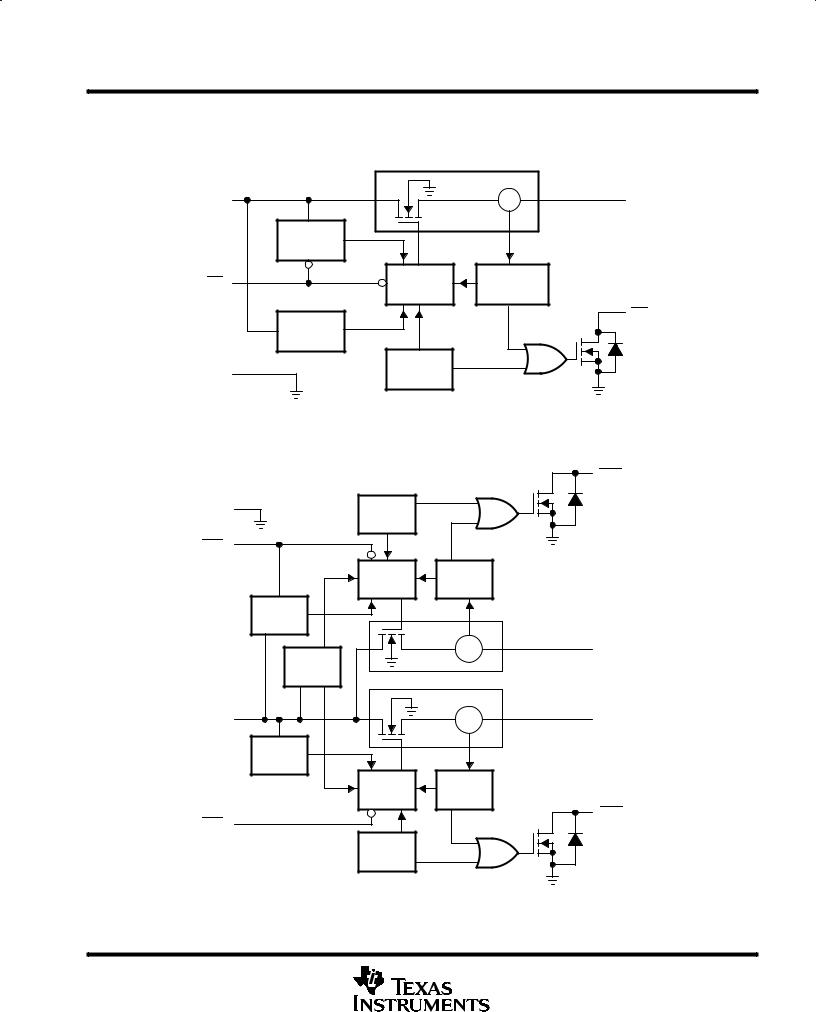
functional block diagrams
TPS2041A
|
Power Switch |
|
|
|
|
² |
|
IN |
|
CS |
OUT |
|
Charge |
|
|
|
Pump |
|
|
EN³ |
Driver |
Current |
|
Limit |
|
||
|
|
|
|
|
|
|
OC |
|
UVLO |
|
|
|
Thermal |
|
|
GND |
Sense |
|
|
²Current sense
³Active high for TPS205xA series
TPS2042A
|
|
|
OC1 |
GND |
Thermal |
|
|
Sense |
|
|
|
|
|
|
|
EN1³ |
|
|
|
|
Driver |
Current |
|
|
Limit |
|
|
|
|
|
|
|
Charge |
|
|
|
Pump |
|
² |
|
|
|
|
|
|
CS |
OUT1 |
|
UVLO |
|
|
|
Power Switch |
|
|
²
IN |
CS |
OUT2 |
Charge |
|
|
Pump |
|
|
Driver |
Current |
|
Limit |
||
|
||
|
OC2 |
EN2³
Thermal |
Sense |
²Current sense
³Active high for TPS205xA series
POST OFFICE BOX 655303 •DALLAS, TEXAS 75265 |
3 |
TPS2041A, TPS2042A, TPS2043A, TPS2044A TPS2051A, TPS2052A, TPS2053A, TPS2054A CURRENT-LIMITED POWER-DISTRIBUTION SWITCHES
SLVS247 ± SEPTEMBER 2000
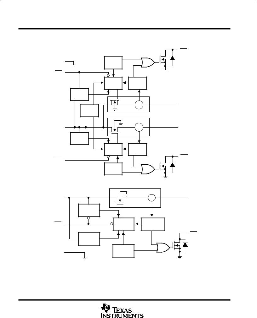
functional block diagrams
TPS2043A
GNDA
OC1
Thermal |
Sense |
EN1³
Driver |
Current |
|
Limit |
|
|
|
|
|
Charge |
|
|
Pump |
|
² |
|
|
|
|
CS |
OUT1 |
UVLO |
|
|
|
Power Switch |
|
²
IN1 |
CS |
OUT2 |
Charge |
|
|
Pump |
|
|
Driver |
Current |
|
Limit |
||
|
||
|
OC2 |
EN2³
Thermal |
Sense |
|
Power Switch |
|
|
|
|
² |
|
IN2 |
|
CS |
OUT3 |
|
Charge |
|
|
|
Pump |
|
|
EN3³ |
Driver |
Current |
|
Limit |
|
||
|
|
|
|
|
|
|
OC3 |
|
UVLO |
|
|
|
Thermal |
|
|
GNDB |
Sense |
|
|
²Current sense
³Active high for TPS205xA series
4 |
POST OFFICE BOX 655303 •DALLAS, TEXAS 75265 |

TPS2041A, TPS2042A, TPS2043A, TPS2044A
TPS2051A, TPS2052A, TPS2053A, TPS2054A
CURRENT-LIMITED POWER-DISTRIBUTION SWITCHES
SLVS247 ± SEPTEMBER 2000
functional block diagrams
TPS2044A |
OC1 |
GNDA |
Thermal |
|
|
Sense |
|
|
|
|
|
|
|
EN1³ |
|
|
|
|
Driver |
Current |
|
|
Limit |
|
|
|
|
|
|
|
Charge |
|
|
|
Pump |
|
² |
|
|
|
|
|
|
CS |
OUT |
|
UVLO |
|
1 |
|
Power Switch |
|
|
|
|
|
² |
IN1 |
|
CS |
OUT |
|
Charge |
|
2 |
|
|
|
|
|
Pump |
|
|
|
Driver |
Current |
|
|
Limit |
|
|
|
|
|
|
EN2³ |
|
|
OC2 |
|
|
|
|
Thermal |
Sense |
OC3
GNDB |
Thermal |
|
Sense |
||
|
EN3³
IN2
EN4³
² Current sense
Driver |
Current |
|
Limit |
|
|
|
|
|
Charge |
|
|
Pump |
|
² |
|
|
|
|
CS |
OUT3 |
UVLO |
|
|
Power Switch |
|
|
²
CS |
OUT4 |
Charge |
|
|
Pump |
|
|
Driver |
Current |
|
Limit |
||
|
||
|
OC4 |
Thermal |
Sense |
³ Active high for TPS205xA series
POST OFFICE BOX 655303 •DALLAS, TEXAS 75265 |
5 |

TPS2041A, TPS2042A, TPS2043A, TPS2044A
TPS2051A, TPS2052A, TPS2053A, TPS2054A
CURRENT-LIMITED POWER-DISTRIBUTION SWITCHES
SLVS247 ± SEPTEMBER 2000
|
|
|
|
|
|
|
|
|
|
|
|
Terminal Functions |
TPS2041A and TPS2051A |
|
|
||||||||||
|
|
|
|
|
|
|
|
|
|
|
|
|
|
|
|
|
|
|
|
|
TERMINAL |
|
|
|
|
|
|
|
|
|
|
|
|
|
|
I/O |
DESCRIPTION |
|
|
NAME |
NO. |
||||||||||
|
|
|
|
|
|
|||||||
TPS2041A |
|
TPS2051A |
|
|
||||||||
|
|
|
|
|
|
|
|
|
|
|
||
|
|
|
|
|
|
|
|
|
|
|
|
|
|
|
|
|
|
|
|
|
4 |
|
± |
I |
Enable input. Logic low turns on power switch. |
|
EN |
|
|
|
|
|
|
|
||||
|
EN |
± |
|
4 |
I |
Enable input. Logic high turns on power switch. |
||||||
|
|
|
|
|
|
|
|
|
|
|
|
|
|
GND |
1 |
|
1 |
I |
Ground |
||||||
|
|
|
|
|
|
|
|
|
|
|
|
|
|
IN |
2, 3 |
|
2, 3 |
I |
Input voltage |
||||||
|
|
|
|
|
|
|
|
|
|
|
||
|
|
|
|
|
|
|
|
5 |
|
5 |
O |
Overcurrent. Logic output active low |
|
OC |
|
|
|
|
|
|
|||||
|
|
|
|
|
|
|
|
|
|
|
||
|
OUT |
6, 7, 8 |
|
6, 7, 8 |
O |
Power-switch output |
||||||
|
|
|
|
|
|
|
|
|
|
|
|
|
TPS2042A and TPS2052A |
|
|
||||||||||
|
|
|
|
|
|
|
|
|
|
|
|
|
|
|
|
|
|
|
|
|
TERMINAL |
|
|
|
|
|
|
|
|
|
|
|
|
|
I/O |
DESCRIPTION |
||
|
NAME |
NO. |
||||||||||
|
|
|
|
|
|
|||||||
|
TPS2042A |
|
TPS2052A |
|
|
|||||||
|
|
|
|
|
|
|
|
|
|
|
||
|
|
|
|
|
|
|
|
|
|
|||
|
|
|
|
|
|
|
|
3 |
|
± |
I |
Enable input. Logic low turns on power switch, IN-OUT1. |
|
EN1 |
|
|
|
|
|
||||||
|
|
|
|
|
|
|
|
|
||||
|
|
|
|
|
|
|
|
4 |
|
± |
I |
Enable input. Logic low turns on power switch, IN-OUT2. |
|
EN2 |
|
|
|
|
|||||||
|
|
|
|
|
|
|
|
|
||||
|
EN1 |
± |
|
3 |
I |
Enable input. Logic high turns on power switch, IN-OUT1. |
||||||
|
|
|
|
|
|
|
|
|
||||
|
EN2 |
± |
|
4 |
I |
Enable input. Logic high turns on power switch, IN-OUT2. |
||||||
|
|
|
|
|
|
|
|
|
||||
|
GND |
1 |
|
1 |
I |
Ground |
||||||
|
|
|
|
|
|
|
|
|
||||
|
IN |
2 |
|
2 |
I |
Input voltage |
||||||
|
|
|
|
|
|
|
|
|||||
|
|
|
|
|
|
|
|
8 |
|
8 |
O |
Overcurrent. Logic output active low, for power switch, IN-OUT1 |
|
OC1 |
|
|
|
||||||||
|
|
|
|
|
|
|
||||||
|
|
|
|
|
|
|
|
5 |
|
5 |
O |
Overcurrent. Logic output active low, for power switch, IN-OUT2 |
|
OC2 |
|
|
|||||||||
|
|
|
|
|
|
|
||||||
|
OUT1 |
7 |
|
7 |
O |
Power-switch output |
||||||
|
|
|
|
|
|
|
||||||
|
OUT2 |
6 |
|
6 |
O |
Power-switch output |
||||||
6 |
POST OFFICE BOX 655303 •DALLAS, TEXAS 75265 |

|
|
|
|
|
|
|
|
|
|
|
TPS2041A, TPS2042A, TPS2043A, TPS2044A |
|
|
|
|
|
|
|
|
|
|
|
|
TPS2051A, TPS2052A, TPS2053A, TPS2054A |
|
|
|
|
|
|
|
|
|
|
|
|
CURRENT-LIMITED POWER-DISTRIBUTION SWITCHES |
|
|
|
|
|
|
|
|
|
|
|
|
SLVS247 ± SEPTEMBER 2000 |
|
|
|
|
|
|
|
|
|
|
|
|
|
|
|
|
|
|
|
|
|
|
|
|
|
Terminal Functions (Continued) |
|
TPS2043A and TPS2053A |
|
|
|
|||||||||
|
|
|
|
|
|
|
|
|
|
|
|
|
|
|
|
|
|
|
|
TERMINAL |
|
|
|
|
|
|
|
|
|
|
|
|
|
|
I/O |
DESCRIPTION |
|
|
|
NAME |
NO. |
|
|||||||||
|
|
|
|
|
|
|
||||||
TPS2043A |
|
TPS2053A |
|
|
|
|||||||
|
|
|
|
|
|
|
|
|
|
|
||
|
|
|
|
|
|
|
|
|
|
|
|
|
|
|
|
|
|
|
|
3 |
|
± |
I |
Enable input, logic low turns on power switch, IN1-OUT1. |
|
|
EN1 |
|
|
|
|
|
|
|||||
|
|
|
|
|
|
|
|
|
|
|
||
|
|
|
|
|
|
|
4 |
|
± |
I |
Enable input, logic low turns on power switch, IN1-OUT2. |
|
|
EN2 |
|
|
|
|
|
||||||
|
|
|
|
|
|
|
|
|
|
|
||
|
|
|
|
|
|
|
7 |
|
± |
I |
Enable input, logic low turns on power switch, IN2-OUT3. |
|
|
EN3 |
|
|
|
|
|
||||||
|
|
|
|
|
|
|
|
|
|
|
||
|
EN1 |
± |
|
3 |
I |
Enable input, logic high turns on power switch, IN1-OUT1. |
|
|||||
|
|
|
|
|
|
|
|
|
|
|
||
|
EN2 |
± |
|
4 |
I |
Enable input, logic high turns on power switch, IN1-OUT2. |
|
|||||
|
|
|
|
|
|
|
|
|
|
|
||
|
EN3 |
± |
|
7 |
I |
Enable input, logic high turns on power switch, IN2-OUT3. |
|
|||||
|
|
|
|
|
|
|
|
|
|
|
||
|
GNDA |
1 |
|
1 |
|
Ground for IN1 switch and circuitry. |
|
|||||
|
|
|
|
|
|
|
|
|
|
|
||
|
GNDB |
5 |
|
5 |
|
Ground for IN2 switch and circuitry. |
|
|||||
|
|
|
|
|
|
|
|
|
|
|
||
|
IN1 |
2 |
|
2 |
I |
Input voltage |
|
|||||
|
|
|
|
|
|
|
|
|
|
|
||
|
IN2 |
6 |
|
6 |
I |
Input voltage |
|
|||||
|
|
|
|
|
|
|
|
|
|
|||
|
|
|
|
|
|
|
8, 9, 10 |
|
8, 9, 10 |
|
No connection |
|
|
NC |
|
|
|
|
|
|
|||||
|
|
|
|
|
|
|
16 |
|
16 |
O |
Overcurrent, logic output active low, IN1-OUT1 |
|
|
OC1 |
|
|
|
|
|||||||
|
|
|
|
|
|
|
|
|||||
|
|
|
|
|
|
|
13 |
|
13 |
O |
Overcurrent, logic output active low, IN1-OUT2 |
|
|
OC2 |
|
|
|
||||||||
|
|
|
|
|
|
|
|
|||||
|
|
|
|
|
|
|
12 |
|
12 |
O |
Overcurrent, logic output active low, IN2-OUT3 |
|
|
OC3 |
|
|
|
||||||||
|
|
|
|
|
|
|
|
|||||
|
OUT1 |
15 |
|
15 |
O |
Power-switch output, IN1-OUT1 |
|
|||||
|
|
|
|
|
|
|
|
|||||
|
OUT2 |
14 |
|
14 |
O |
Power-switch output, IN1-OUT2 |
|
|||||
|
|
|
|
|
|
|
|
|||||
|
OUT3 |
11 |
|
11 |
O |
Power-switch output, IN2-OUT3 |
|
|||||
TPS2044A and TPS2054A |
|
|
|
|||||||||
|
|
|
|
|
|
|
|
|
|
|
|
|
|
|
|
|
|
|
|
TERMINAL |
|
|
|
|
|
|
|
|
|
|
|
|
|
|
|
|
||
|
NAME |
NO. |
I/O |
DESCRIPTION |
|
|||||||
|
TPS2044A |
|
TPS2054A |
|
|
|
||||||
|
|
|
|
|
|
|
|
|
|
|
||
|
|
|
|
|
|
|
|
|||||
|
|
|
|
|
|
|
3 |
|
± |
I |
Enable input. logic low turns on power switch, IN1-OUT1. |
|
|
EN1 |
|
|
|
||||||||
|
|
|
|
|
|
|
|
|||||
|
|
|
|
|
|
|
4 |
|
± |
I |
Enable input. Logic low turns on power switch, IN1-OUT2. |
|
|
EN2 |
|
|
|
||||||||
|
|
|
|
|
|
|
|
|||||
|
|
|
|
|
|
|
7 |
|
± |
I |
Enable input. Logic low turns on power switch, IN2-OUT3. |
|
|
EN3 |
|
|
|
||||||||
|
|
|
|
|
|
|
|
|||||
|
|
|
|
|
|
|
8 |
|
± |
I |
Enable input. Logic low turns on power switch, IN2-OUT4. |
|
|
EN4 |
|
|
|
||||||||
|
|
|
|
|
|
|
|
|||||
|
EN1 |
± |
|
3 |
I |
Enable input. Logic high turns on power switch, IN1-OUT1. |
|
|||||
|
|
|
|
|
|
|
|
|||||
|
EN2 |
± |
|
4 |
I |
Enable input. Logic high turns on power switch, IN1-OUT2. |
|
|||||
|
|
|
|
|
|
|
|
|||||
|
EN3 |
± |
|
7 |
I |
Enable input. Logic high turns on power switch, IN2-OUT3. |
|
|||||
|
|
|
|
|
|
|
|
|||||
|
EN4 |
± |
|
8 |
I |
Enable input. Logic high turns on power switch, IN2-OUT4. |
|
|||||
|
|
|
|
|
|
|
|
|||||
|
GNDA |
1 |
|
1 |
|
Ground for IN1 switch and circuitry. |
|
|||||
|
|
|
|
|
|
|
|
|||||
|
GNDB |
5 |
|
5 |
|
Ground for IN2 switch and circuitry. |
|
|||||
|
|
|
|
|
|
|
|
|||||
|
IN1 |
2 |
|
2 |
I |
Input voltage |
|
|||||
|
|
|
|
|
|
|
|
|||||
|
IN2 |
6 |
|
6 |
I |
Input voltage |
|
|||||
|
|
|
|
|
|
|
|
|||||
|
|
|
|
|
|
|
16 |
|
16 |
O |
Overcurrent. Logic output active low, IN1-OUT1 |
|
|
OC1 |
|
|
|
||||||||
|
|
|
|
|
|
|
|
|||||
|
|
|
|
|
|
|
13 |
|
13 |
O |
Overcurrent. Logic output active low, IN1-OUT2 |
|
|
OC2 |
|
|
|
||||||||
|
|
|
|
|
|
|
12 |
|
12 |
O |
Overcurrent. Logic output active low, IN2-OUT3 |
|
|
OC3 |
|
|
|
||||||||
|
|
|
|
|
|
|
|
|||||
|
|
|
|
|
|
|
9 |
|
9 |
O |
Overcurrent. Logic output active low, IN2-OUT4 |
|
|
OC4 |
|
|
|
||||||||
|
|
|
|
|
|
|
|
|||||
|
OUT1 |
15 |
|
15 |
O |
Power-switch output, IN1-OUT1 |
|
|||||
|
|
|
|
|
|
|
|
|||||
|
OUT2 |
14 |
|
14 |
O |
Power-switch output, IN1-OUT2 |
|
|||||
|
|
|
|
|
|
|
|
|||||
|
OUT3 |
11 |
|
11 |
O |
Power-switch output, IN2-OUT3 |
|
|||||
|
|
|
|
|
|
|
|
|||||
|
OUT4 |
10 |
|
10 |
O |
Power-switch output, IN2-OUT4 |
|
|||||
|
|
|
|
|
|
|
|
|
|
|
|
|
|
|
|
|
|
|
|
|
|
|
|
|
|
POST OFFICE BOX 655303 •DALLAS, TEXAS 75265 |
7 |

TPS2041A, TPS2042A, TPS2043A, TPS2044A
TPS2051A, TPS2052A, TPS2053A, TPS2054A
CURRENT-LIMITED POWER-DISTRIBUTION SWITCHES
SLVS247 ± SEPTEMBER 2000
detailed description
power switch
The power switch is an N-channel MOSFET with a maximum on-state resistance of 135 mΩ (VI(IN) = 5 V). Configured as a high-side switch, the power switch prevents current flow from OUT to IN and IN to OUT when
disabled. The power switch supplies a minimum of 500 mA per switch.
charge pump
An internal charge pump supplies power to the driver circuit and provides the necessary voltage to pull the gate of the MOSFET above the source. The charge pump operates from input voltages as low as 2.7 V and requires very little supply current.
driver
The driver controls the gate voltage of the power switch. To limit large current surges and reduce the associated electromagnetic interference (EMI) produced, the driver incorporates circuitry that controls the rise times and fall times of the output voltage. The rise and fall times are typically in the 2-ms to 4-ms range.
enable (ENx, ENx)
The logic enable disables the power switch and the bias for the charge pump, driver, and other circuitry to reduce the supply current. The supply current is reduced to less than 10 µA on the single and dual devices (20 µA on the triple and quad devices) when a logic high is present on ENx (TPS204xA² ) or a logic low is present on ENx (TPS205xA² ). A logic zero input on ENx or a logic high on ENx restores bias to the drive and control circuits and turns the power on. The enable input is compatible with both TTL and CMOS logic levels.
overcurrent (OCx)
The OCx open-drain output is asserted (active low) when an overcurrent or overtemperature condition is encountered. The output will remain asserted until the overcurrent or overtemperature condition is removed.
current sense
A sense FET monitors the current supplied to the load. The sense FET measures current more efficiently than conventional resistance methods. When an overload or short circuit is encountered, the current-sense circuitry sends a control signal to the driver. The driver in turn reduces the gate voltage and drives the power FET into its saturation region, which switches the output into a constant-current mode and holds the current constant while varying the voltage on the load.
thermal sense
The TPS204xA and TPS205xA implement a dual-threshold thermal trip to allow fully independent operation of the power distribution switches. In an overcurrent or short-circuit condition the junction temperature rises. When the die temperature rises to approximately 140°C, the internal thermal sense circuitry checks to determine which power switch is in an overcurrent condition and turns off that switch, thus isolating the fault without interrupting operation of the adjacent power switch. Hysteresis is built into the thermal sense, and after the device has cooled approximately 20 degrees, the switch turns back on. The switch continues to cycle off and on until the fault is removed. The (OCx) open-drain output is asserted (active low) when overtemperature or overcurrent occurs.
undervoltage lockout
A voltage sense circuit monitors the input voltage. When the input voltage is below approximately 2 V, a control signal turns off the power switch.
²Product series designations TPS204x and TPS205x refer to devices presented in this data sheet and not necessarily to other TI devices numbered in this sequence.
8 |
POST OFFICE BOX 655303 •DALLAS, TEXAS 75265 |

TPS2041A, TPS2042A, TPS2043A, TPS2044A
TPS2051A, TPS2052A, TPS2053A, TPS2054A
CURRENT-LIMITED POWER-DISTRIBUTION SWITCHES
SLVS247 ± SEPTEMBER 2000
absolute maximum ratings over operating free-air temperature range (unless otherwise noted)²
Input voltage range, VI(IN) (see Note 1) . . . . . . . . . . . . . . . . . . . . . . . . . . . . . . . . . . . . . . . . . . . . . . . . ±0.3 V to 6 V Output voltage range, VO(OUT) (see Note 1) . . . . . . . . . . . . . . . . . . . . . . . . . . . . . . . . . . . ±0.3 V to VI(IN) + 0.3 V Input voltage range, VI(ENx) or VI(ENx) . . . . . . . . . . . . . . . . . . . . . . . . . . . . . . . . . . . . . . . . . . . . . . . . ±0.3 V to 6 V Continuous output current, IO(OUT) . . . . . . . . . . . . . . . . . . . . . . . . . . . . . . . . . . . . . . . . . . . . . . . . . internally limited Continuous total power dissipation . . . . . . . . . . . . . . . . . . . . . . . . . . . . . . . . . . . . . . See Dissipation Rating Table
Operating virtual junction temperature range, TJ . . . . . . . . . . . . . . . . . . . . . . . . . . . . . . . . . . . . . . . . 0°C to 125°C Storage temperature range, Tstg . . . . . . . . . . . . . . . . . . . . . . . . . . . . . . . . . . . . . . . . . . . . . . . . . . . . ±65°C to 150°C Lead temperature soldering 1,6 mm (1/16 inch) from case for 10 seconds . . . . . . . . . . . . . . . . . . . . . . . 260°C
Electrostatic discharge (ESD) protection: Human body model MIL-STD-883C . . . . . . . . . . . . . . . . . . . . . 2 kV Machine model . . . . . . . . . . . . . . . . . . . . . . . . . . . . . . . . . . . . . 0.2 kV
²Stresses beyond those listed under ªabsolute maximum ratingsº may cause permanent damage to the device. These are stress ratings only, and functional operation of the device at these or any other conditions beyond those indicated under ªrecommended operating conditionsº is not
implied. Exposure to absolute-maximum-rated conditions for extended periods may affect device reliability. NOTE 1: All voltages are with respect to GND.
|
|
DISSIPATION RATING TABLE |
|
||
PACKAGE |
TA ≤ 25°C |
DERATING FACTOR |
TA = 70°C |
TA = 85°C |
|
POWER RATING |
ABOVE TA = 25°C |
POWER RATING |
POWER RATING |
||
|
|||||
D±8 |
725 mW |
5.9 mW/°C |
464 mW |
377 mW |
|
D±16 |
1123 mW |
9 mW/°C |
719 mW |
584 mW |
|
recommended operating conditions
|
|
|
MIN |
MAX |
UNIT |
|
|
|
|
|
|
Input voltage, VI(IN) |
2.7 |
5.5 |
V |
||
|
|
|
|
|
|
Input voltage, VI(EN) |
or VI(EN) |
0 |
5.5 |
V |
|
Continuous output current, IO(OUT) (per switch) |
0 |
500 |
mA |
||
Operating virtual junction temperature, TJ |
0 |
125 |
°C |
||
POST OFFICE BOX 655303 •DALLAS, TEXAS 75265 |
9 |
TPS2041A, TPS2042A, TPS2043A, TPS2044A
TPS2051A, TPS2052A, TPS2053A, TPS2054A
CURRENT-LIMITED POWER-DISTRIBUTION SWITCHES
SLVS247 ± SEPTEMBER 2000
electrical characteristics over recommended operating junction temperature range, VI(IN)= 5.5 V, IO = rated current, VI(EN) = 0 V, VI(EN) = VI(IN) (unless otherwise noted)
power switch
|
PARAMETER |
TEST CONDITIONS² |
TPS204xA |
|
TPS205xA |
|
UNIT |
|
|
|
|
|
|
||||
|
MIN TYP |
MAX |
MIN TYP |
MAX |
||||
|
|
|
|
|
||||
|
|
|
|
|
|
|
|
|
|
|
VI(IN) = 5 V, |
TJ = 25°C, |
80 |
100 |
80 |
100 |
|
|
|
IO = 0.5 A |
|
|
||||
|
|
|
|
|
|
|
|
|
|
Static drain-source on-state |
VI(IN) = 5 V, |
TJ = 85°C, |
90 |
120 |
90 |
120 |
|
|
resistance, 5-V operation |
IO = 0.5 A |
|
|
||||
|
|
|
|
|
|
|
||
|
|
VI(IN) = 5 V, |
TJ = 125°C, |
100 |
135 |
100 |
135 |
mΩ |
|
|
IO = 0.5 A |
|
|||||
rDS(on) |
|
|
|
|
|
|
|
|
|
VI(IN) = 3.3 V, |
TJ = 25°C, |
90 |
125 |
90 |
125 |
|
|
|
|
IO = 0.5 A |
|
|
||||
|
|
|
|
|
|
|
|
|
|
Static drain-source on-state |
VI(IN) = 3.3 V, |
TJ = 85°C, |
110 |
145 |
110 |
145 |
|
|
resistance, 3.3-V operation |
IO = 0.5 A |
|
|
||||
|
|
|
|
|
|
|
||
|
|
VI(IN) = 3.3 V, |
TJ = 125°C, |
120 |
160 |
120 |
160 |
|
|
|
IO = 0.5 A |
|
|
||||
|
|
|
|
|
|
|
|
|
|
|
VI(IN) = 5.5 V, |
TJ = 25°C, |
2.5 |
|
2.5 |
|
|
|
|
CL = 1 µF, |
RL=10 Ω |
|
|
|
||
tr |
Rise time, output |
|
|
|
|
ms |
||
VI(IN) = 2.7 V, |
TJ = 25°C, |
3 |
|
3 |
|
|||
|
|
CL = 1 µF, |
RL=10 Ω |
|
|
|
||
|
|
|
|
|
|
|
||
|
|
VI(IN) = 5.5 V, |
TJ = 25°C, |
4.4 |
|
4.4 |
|
|
|
|
CL = 1 µF, |
RL=10 Ω |
|
|
|
||
tf |
Fall time, output |
|
|
|
|
ms |
||
VI(IN) = 2.7 V, |
TJ = 25°C, |
2.5 |
|
2.5 |
|
|||
|
|
|
|
|
||||
|
|
CL = 1 µF, |
RL=10 Ω |
|
|
|
||
|
|
|
|
|
|
|
||
² Pulse-testing techniques maintain junction temperature close to ambient temperature; thermal effects must be taken into account separately.
enable input ENx or ENx
|
PARAMETER |
|
|
TEST CONDITIONS |
TPS204xA |
|
TPS205xA |
|
UNIT |
|||||
|
|
|
|
|
|
|
||||||||
|
|
|
MIN TYP |
MAX |
MIN TYP |
MAX |
||||||||
|
|
|
|
|
|
|
|
|
|
|
||||
|
|
|
|
|
|
|
|
|
|
|
|
|
|
|
VIH |
High-level input voltage |
2.7 |
V ≤ VI(IN) ≤ 5.5 V |
2 |
|
2 |
|
V |
||||||
VIL |
Low-level input voltage |
4.5 |
V ≤ VI(IN) ≤ 5.5 V |
|
0.8 |
|
0.8 |
V |
||||||
2.7 |
V≤ VI(IN) ≤ 4.5 V |
|
0.4 |
|
0.4 |
|
||||||||
|
|
|
|
|
|
|||||||||
II |
Input current |
TPS204xA |
V |
I(ENx) |
= 0 V or V |
I(ENx) |
= VI(IN) |
±0.5 |
0.5 |
|
|
µA |
||
TPS205xA |
VI(ENx) = VI(IN) or VI(ENx) = 0 V |
|
|
±0.5 |
0.5 |
|||||||||
|
|
|
|
|
||||||||||
ton |
Turnon time |
CL = 100 µF, |
RL=10 Ω |
|
20 |
|
20 |
ms |
||||||
toff |
Turnoff time |
CL = 100 µF, |
RL=10 Ω |
|
40 |
|
40 |
|
||||||
current limit
PARAMETER |
TEST CONDITIONS² |
TPS204xA |
|
TPS205xA |
|
UNIT |
|||
|
|
|
|
|
|
||||
MIN |
TYP |
MAX |
MIN |
TYP |
MAX |
||||
|
|
|
|||||||
|
|
|
|
|
|
|
|
|
|
IOS Short-circuit output current |
VI(IN) = 5 V, OUT connected to GND, |
0.7 |
1 |
1.3 |
0.7 |
1 |
1.3 |
A |
|
Device enabled into short circuit |
|||||||||
|
|
|
|
|
|
|
|
||
² Pulse-testing techniques maintain junction temperature close to ambient temperature; thermal effects must be taken into account separately.
10 |
POST OFFICE BOX 655303 •DALLAS, TEXAS 75265 |
TPS2041A, TPS2042A, TPS2043A, TPS2044A
TPS2051A, TPS2052A, TPS2053A, TPS2054A
CURRENT-LIMITED POWER-DISTRIBUTION SWITCHES
SLVS247 ± SEPTEMBER 2000
electrical characteristics over recommended operating junction temperature range, VI(IN)= 5.5 V, IO = rated current, VI(EN) = 0 V, VI(EN) = VI(IN) (unless otherwise noted) (continued)
supply current (TPS2041A, TPS2051A)
PARAMETER |
|
|
TEST CONDITIONS |
|
|
|
|
TPS2041A |
|
TPS2051A |
|
UNIT |
||||
|
|
|
|
|
|
|
|
|
|
|
||||||
|
|
|
|
|
MIN |
TYP |
MAX |
MIN TYP |
MAX |
|||||||
|
|
|
|
|
|
|
|
|
|
|
|
|||||
|
|
|
|
|
|
|
|
|
|
|
|
|
|
|
||
|
|
|
|
|
|
TJ = 25°C |
|
|
|
0.025 |
1 |
|
|
|
||
|
|
VI(EN) |
|
= VI(IN) |
|
|
|
|
|
|
|
|
|
|
|
|
Supply current, low-level |
No Load |
|
° |
≤ |
TJ |
≤ |
° |
|
|
10 |
|
|
|
|||
|
|
|
|
±40 C |
|
|
125 C |
|
|
|
|
A |
||||
output |
on OUT |
|
|
|
|
|
° |
|
|
|
|
|
|
0.025 |
1 |
|
|
|
|
|
|
|
|
|
|
|
|
|
|||||
|
|
VI(EN) |
= 0 V |
TJ = 25 C |
|
|
|
|
|
|
||||||
|
|
±40°C |
≤ TJ |
≤ 125°C |
|
|
|
|
10 |
|
||||||
|
|
|
|
|
|
|
|
|
|
|
||||||
|
|
|
|
|
|
TJ = 25°C |
|
|
|
85 |
110 |
|
|
|
||
|
|
VI(EN) |
= 0 V |
|
|
|
|
|
|
|||||||
Supply current, |
No Load |
±40°C |
≤ TJ |
≤ 125°C |
|
100 |
|
|
|
A |
||||||
|
|
|
|
|
|
|
|
|||||||||
high-level output |
on OUT |
|
|
|
|
|
° |
|
|
|
|
|
|
85 |
110 |
|
|
|
|
|
|
|
|
|
|
|
|
|
|||||
|
|
VI(EN) |
= VI(IN) |
TJ = 25 C |
|
|
|
|
|
|
||||||
|
|
±40°C |
≤ TJ |
≤ 125°C |
|
|
|
100 |
|
|
||||||
|
|
|
|
|
|
|
|
|
|
|
||||||
|
OUT |
|
|
|
|
° |
≤ |
|
≤ |
° |
|
|
|
|
|
|
|
VI(EN) |
= VI(IN) |
TJ |
|
100 |
|
|
|
|
|||||||
Leakage current |
connected |
±40 C |
|
|
125 C |
|
|
|
|
A |
||||||
VI(EN)= 0 V |
±40°C ≤ TJ ≤ 125°C |
|
|
|
100 |
|
||||||||||
|
to ground |
|
|
|
|
|
||||||||||
|
|
|
|
|
|
|
|
|
|
|
|
|
|
|
|
|
Reverse leakage current |
IN = High |
VI(EN |
) = 0 V |
TJ = 25°C |
|
|
|
0.3 |
|
|
|
A |
||||
impedance |
VI(EN) |
= VI(IN) |
|
|
|
|
|
0.3 |
|
|||||||
|
|
|
|
|
|
|
|
|
|
|
|
|||||
supply current (TPS2042A, TPS2052A)
PARAMETER |
|
|
TEST CONDITIONS |
|
|
|
|
TPS2042A |
|
TPS2052A |
|
UNIT |
||||
|
|
|
|
|
|
|
|
|
|
|
||||||
|
|
|
|
|
MIN |
TYP |
MAX |
MIN TYP |
MAX |
|||||||
|
|
|
|
|
|
|
|
|
|
|
|
|||||
|
|
|
|
|
|
|
|
|
|
|
|
|
|
|
||
|
|
V |
|
|
= VI(IN) |
TJ = 25°C |
|
|
|
0.025 |
1 |
|
|
|
||
|
|
I(ENx) |
|
|
|
|
|
|
|
|
|
|
|
|||
Supply current, low-level |
No Load |
° |
≤ |
TJ |
≤ |
° |
|
|
10 |
|
|
|
||||
|
|
|
|
±40 C |
|
|
125 C |
|
|
|
|
A |
||||
output |
on OUT |
|
|
|
|
|
° |
|
|
|
|
|
|
0.025 |
1 |
|
|
|
VI(ENx) = 0 V |
TJ = 25 C |
|
|
|
|
|
|
|||||||
|
|
±40°C |
≤ TJ |
≤ 125°C |
|
|
|
|
10 |
|
||||||
|
|
|
|
|
|
|
|
|
|
|
||||||
|
|
|
|
|
|
TJ = 25°C |
|
|
|
85 |
110 |
|
|
|
||
|
|
VI(ENx) = 0 V |
|
|
|
|
|
|
||||||||
Supply current, |
No Load |
±40°C |
≤ TJ |
≤ 125°C |
|
100 |
|
|
|
A |
||||||
|
|
|
|
|
|
|
|
|||||||||
high-level output |
on OUT |
|
|
|
|
|
° |
|
|
|
|
|
|
85 |
110 |
|
|
|
VI(ENx) = VI(IN) |
TJ = 25 C |
|
|
|
|
|
|
|||||||
|
|
±40°C |
≤ TJ |
≤ 125°C |
|
|
|
100 |
|
|
||||||
|
|
|
|
|
|
|
|
|
|
|
||||||
|
OUT |
|
|
|
|
° |
≤ |
|
≤ |
° |
|
|
|
|
|
|
|
VI(ENx) = VI(IN) |
TJ |
|
100 |
|
|
|
|
||||||||
Leakage current |
connected |
±40 C |
|
|
125 C |
|
|
|
|
A |
||||||
VI(ENx) = 0 V |
±40°C ≤ TJ ≤ 125°C |
|
|
|
100 |
|
||||||||||
|
to ground |
|
|
|
|
|
||||||||||
|
|
|
|
|
|
|
|
|
|
|
|
|
|
|
|
|
Reverse leakage current |
IN = high |
VI(EN) |
= 0 V |
TJ = 25°C |
|
|
|
0.3 |
|
|
|
A |
||||
impedance |
VI(EN) = VI(IN) |
|
|
|
|
|
0.3 |
|
||||||||
|
|
|
|
|
|
|
|
|
|
|
|
|||||
POST OFFICE BOX 655303 •DALLAS, TEXAS 75265 |
11 |
 Loading...