


Texas Instruments TPS2216ADB, TPS2216ADAPR, TPS2216ADAP, TPS2214ADBR, TPS2214ADB Datasheet
...TPS2214A, TPS2216A LOW-COST DUAL-SLOT PC CARD POWER SWITCH FOR SERIAL PCMCIA CONTROLLERS
SLVS267 ± DECEMBER 1999
DFully Integrated xVCC and xVPP Switching
DxVPP Programmed Independent of xVCC
D3.3-V, 5-V, and/or 12-V Power Distribution
DLow rDS(on) (60-mΩ 3.3-V xVCC Switch and 140-mΩ 5-V xVCC Switch Typical)
DShort Circuit and Thermal Protection
D150-µA (maximum) Quiescent Current
DStandby Mode: 50-mA Current Limit (Typ)
D12-V Supply Can Be Disabled
D3.3-V Low-Voltage Mode
DAmbient Temperature . . . ±40°C to 70°C
DMeets PC Card Standards
DTTL-Logic Compatible Inputs
DAvailable in 24-Pin and 30-Pin SSOP (DB), and 32-Pin TSSOP (DAP) Packages
DBreak-Before-Make Switching
DInternal Power-On Reset
description
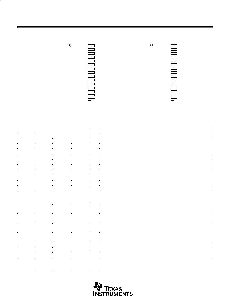
TPS2214A
DB PACKAGE (TOP VIEW)
|
5 V |
|
|
1 |
24 |
|
|
5 V |
|
|
|
|
|
|
|||||
|
|
|
|
|
|||||
|
5 V |
|
|
2 |
23 |
|
|
NC |
|
|
|
|
|
|
|||||
|
|
|
|
|
|||||
|
DATA |
|
3 |
22 |
|
|
MODE |
||
|
|
|
|
|
|||||
CLOCK |
|
|
4 |
21 |
|
|
NC |
||
|
|
|
|
||||||
|
LATCH |
|
|
5 |
20 |
|
|
12 V |
|
|
|
|
|
|
|||||
|
|
|
|
|
|||||
RESET |
|
|
6 |
19 |
|
|
BVPP |
||
|
|
|
|
||||||
|
|
|
|
||||||
|
12V |
|
|
7 |
18 |
|
|
BVCC |
|
|
|
|
|
|
|||||
|
|
|
|
|
|||||
|
AVPP |
|
|
8 |
17 |
|
|
BVCC |
|
|
|
|
|
|
|||||
|
|
|
|
|
|||||
|
AVCC |
|
|
9 |
16 |
|
|
STBY |
|
|
|
|
|
|
|||||
|
|
|
|
|
|||||
|
AVCC |
|
|
10 |
15 |
|
|
OC |
|
|
|
|
|
|
|||||
|
GND |
|
|
11 |
14 |
|
|
3.3 V |
|
|
|
|
|
|
|||||
|
RESET |
|
|
|
12 |
13 |
|
|
3.3 V |
|
|
|
|
|
|
||||
|
|
|
|
|
|
|
|
|
|
NC ± No internal connection
PINOUTS FOR TPS2216A DAP AND DB PACKAGES ARE PROVIDED ON PAGE 2.
The TPS2214A and TPS2216A PC Card power-interface switches provide an integrated power-management solution for two PC Cards. All of the discrete power MOSFETs, a logic section, current limiting, and thermal protection for PC Card control are combined on single integrated circuits. These low-cost devices allow the distribution of 3.3-V, 5-V, and/or 12-V power to the card. The current-limiting feature eliminates the need for fuses. Current-limit reporting can help the user isolate a system fault.
The TPS2214A and TPS2216A feature a 3.3-V low-voltage mode that allows for 3.3-V switching without the need for 5-V power. This feature facilitates low-power system designs such as sleep modes where only 3.3 V is available. These devices also have the ability to program the xVPP outputs independent of the xVCC outputs. A standby mode that changes all output-current limits to 50 mA (typical) has been incorporated.
End-equipment applications for these products include: notebook computers, desktop computers, personal digital assistants (PDAs), digital cameras, and bar-code scanners.
The TPS2216A is backward-compatible with the TPS2202A, TPS2206, and TPS2216. The TPS2214A is backward-compatible with the TPS2214.
|
AVAILABLE OPTIONS |
|
|
|
PACKAGED DEVICES² |
||
TA |
PLASTIC SMALL OUTLINE |
PowerPAD PLASTIC SMALL |
|
OUTLINE |
|||
|
(DB) |
||
|
(DAP) |
||
|
|
||
|
|
|
|
± 40°C to 70°C |
TPS2214ADB(R), TPS2216ADB(R) |
TPS2216ADAP(R) |
|
²The DB and DAP packages are available in tubes and left-end taped and reeled. Add R suffix to device type (e.g., TPS2216ADBR) for taped and reeled.
Please be aware that an important notice concerning availability, standard warranty, and use in critical applications of Texas Instruments semiconductor products and disclaimers thereto appears at the end of this data sheet.
PowerPAD is a trademark of Texas Instruments Incorporated.
PC Card is a trademark of PCMCIA (Personal Computer Memory Card International Association).
PRODUCTION DATA information is current as of publication date. Products conform to specifications per the terms of Texas Instruments standard warranty. Production processing does not necessarily include testing of all parameters.
Copyright 1999, Texas Instruments Incorporated
POST OFFICE BOX 655303 •DALLAS, TEXAS 75265 |
1 |
TPS2214A, TPS2216A
LOW-COST DUAL-SLOT PC CARD POWER SWITCH
FOR SERIAL PCMCIA CONTROLLERS
SLVS267 ± DECEMBER 1999
|
|
|
|
|
TPS2216A |
|
|
|
|
|
|
|
|
|
|
TPS2216A |
|
|
|
|
|||
|
|
|
|
|
DAP PACKAGE |
|
|
|
|
|
|
|
|
|
|
DB PACKAGE |
|
|
|
|
|||
|
|
|
|
|
(TOP VIEW) |
|
|
|
|
|
|
|
|
|
|
(TOP VIEW) |
|
|
|
|
|||
|
5V |
|
|
|
|
|
|
5V |
|
5V |
|
|
|
|
|
|
|
|
5V |
||||
|
|
|
1 |
32 |
|
|
|
|
|
|
1 |
30 |
|
|
|
||||||||
|
|
|
|
|
|
|
|
||||||||||||||||
|
|
|
|
|
|
|
|
|
|||||||||||||||
|
5V |
|
2 |
31 |
|
|
NC |
|
5V |
|
|
2 |
29 |
|
|
|
MODE |
||||||
|
|
|
|
|
|
|
|
||||||||||||||||
|
|
|
|
|
|
|
|
||||||||||||||||
|
NC |
|
3 |
30 |
|
|
MODE |
|
DATA |
|
|
3 |
28 |
|
|
|
NC |
||||||
|
|
|
|
|
|
|
|
||||||||||||||||
|
|
|
|
|
|
|
|
||||||||||||||||
|
DATA |
|
4 |
29 |
|
|
NC |
CLOCK |
|
|
4 |
27 |
|
|
|
NC |
|||||||
|
|
|
|
|
|
|
|||||||||||||||||
|
|
|
|
|
|
|
|||||||||||||||||
CLOCK |
|
|
5 |
28 |
|
|
NC |
|
LATCH |
|
|
|
5 |
26 |
|
|
|
NC |
|||||
|
|
|
|
|
|
|
|
||||||||||||||||
|
LATCH |
|
|
6 |
27 |
|
|
NC |
|
RESET |
|
|
|
6 |
25 |
|
|
|
NC |
||||
|
|
|
|
|
|
|
|
|
|||||||||||||||
|
RESET |
|
7 |
26 |
|
|
NC |
|
12V |
|
|
7 |
24 |
|
|
|
12V |
||||||
|
|
|
|
|
|
|
|
||||||||||||||||
|
|
|
|
|
|
|
|
||||||||||||||||
|
12V |
|
|
8 |
25 |
|
|
12V |
|
AVPP |
|
|
8 |
23 |
|
|
|
BVPP |
|||||
|
|
|
|
|
|
|
|
||||||||||||||||
|
AVPP |
|
9 |
24 |
|
|
BVPP |
|
AVCC |
|
|
9 |
22 |
|
|
|
BVCC |
||||||
|
|
|
|
|
|
|
|
||||||||||||||||
|
|
|
|
|
|
|
|
||||||||||||||||
|
AVCC |
|
10 |
23 |
|
|
BVCC |
|
AVCC |
|
|
10 |
21 |
|
|
|
BVCC |
||||||
|
|
|
|
|
|
|
|
||||||||||||||||
|
|
|
|
|
|
|
|
||||||||||||||||
|
AVCC |
|
11 |
22 |
|
|
BVCC |
|
AVCC |
|
|
11 |
20 |
|
|
|
BVCC |
||||||
|
|
|
|
|
|
|
|
||||||||||||||||
|
|
|
|
|
|
|
|
||||||||||||||||
|
AVCC |
|
|
12 |
21 |
|
|
BVCC |
|
GND |
|
|
12 |
19 |
|
|
|
STBY |
|||||
|
|
|
|
|
|
|
|
||||||||||||||||
|
GND |
|
|
13 |
20 |
|
|
OC |
|
NC |
|
|
13 |
18 |
|
|
|
OC |
|||||
|
|
|
|
|
|
|
|
||||||||||||||||
|
RESET |
|
|
|
14 |
19 |
|
|
|
STBY |
|
|
RESET |
|
|
|
|
14 |
17 |
|
|
|
3.3V |
|
|
|
|
|
|
|
|
|
|
|
|
|
|||||||||||
|
NC |
|
15 |
18 |
|
|
3.3V |
|
3.3V |
|
|
15 |
16 |
|
|
|
3.3V |
||||||
|
|
|
|
|
|
|
|
|
|
|
|||||||||||||
|
3.3V |
|
16 |
17 |
|
|
3.3V |
|
|
|
|
|
|
|
|
|
|
|
|
||||
|
|
|
|
|
|
|
|
|
|
|
|
|
|
|
|
|
|||||||
|
|
|
|
|
|
|
|
|
|
|
|
|
|
|
|
|
|||||||
|
|
|
|
|
|
|
|
|
|
|
|
|
|
|
|
|
|
|
|
|
|
|
|
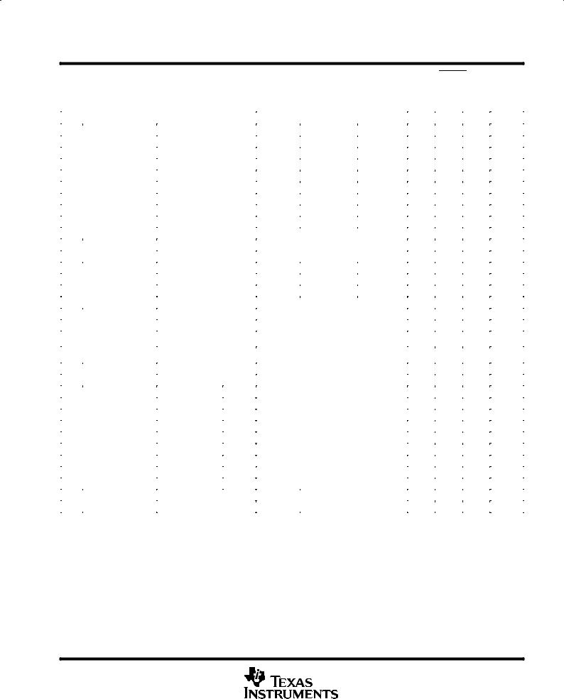
NC ± No internal connection
Terminal Functions
|
|
|
|
|
TERMINAL |
|
|
|
|
|
|
|
|
|
|
|
|
|
|
|
|
|
|
|
|
|
|
|
|
|
|
NO. |
|
I/O |
DESCRIPTION |
|
||
|
NAME |
|
|
|
|
|||||||
|
TPS2214 |
TPS2216 |
|
|||||||||
|
|
|
|
|
|
|||||||
|
|
|
|
|
|
|
|
|
|
|
|
|
|
|
|
|
|
DB-24 |
DB-30 |
DAP |
|
|
|
|
|
|
|
|
|
|
|
|
|
|
|
|
|
|
|
3.3V |
13, 14 |
15, 16, 17 |
16, 17, 18 |
I |
3.3-V input for card power and/or chip power if 5 V is not present |
|
|||||
|
|
|
|
|
|
|
|
|
|
|
|
|
|
5V |
1, 2, 24 |
1, 2, 30 |
1, 2, 32 |
I |
5-V input for card power and/or chip power |
|
|||||
|
|
|
|
|
|
|
|
|
|
|
|
|
|
12V |
7, 20 |
7, 24 |
8, 25 |
I |
12-V Vpp input card power |
|
|||||
|
AVCC |
9, 10 |
9, 10, 11 |
10, 11, 12 |
O |
VCC output: 3.3-V, 5-V, GND or high impedance to card |
|
|||||
|
|
|
|
|
|
|
|
|
|
|
|
|
|
AVPP |
8 |
8 |
9 |
O |
VPP output: 3.3-V, 5-V, 12-V, GND or high impedance to card |
|
|||||
|
|
|
|
|
|
|
|
|
|
|
|
|
|
BVCC |
17, 18 |
20, 21, 22 |
21, 22, 23 |
O |
VCC output: 3.3-V, 5-V, GND or high impedance to card |
|
|||||
|
|
|
|
|
|
|
|
|
|
|
|
|
|
BVPP |
19 |
23 |
24 |
O |
VPP output: 3.3-V, 5-V, 12-V, GND or high impedance to card |
|
|||||
|
|
|
|
|
|
|
|
|
|
|
|
|
|
GND |
11 |
12 |
13 |
|
Ground |
|
|||||
|
|
|
|
|
|
|
|
|
|
|
|
|
|
MODE |
22 |
29 |
30 |
I |
TPS2206 operation when floating or pulled low; must be pulled high externally for |
|
|||||
|
|
|
|
|
|
|
|
|
TPS2216A operation. MODE is internally pulled low with a 150-kΩ pulldown |
|
||
|
|
|
|
|
|
|
|
|
resistor. |
|
||
|
|
|
|
|
|
|
|
|
|
|
|
|
|
|
|
|
|
15 |
18 |
20 |
O |
Logic-level output that goes low when an overcurrent or overtemperature condition |
|
||
|
OC |
|
|
|
|
|||||||
|
|
|
|
|
|
|
|
|
exists. |
|
||
|
|
|
|
|
|
|
|
|
|
|
|
|
|
|
|
|
|
|
|
|
|
|
|||
|
RESET |
6 |
6 |
7 |
I |
Logic-level reset input active high. Do not connect if |
RESET |
pin is used. RESET |
|
|||
|
|
|
|
|
|
|
|
|
is internally pulled low with a 150-kΩ pulldown resistor. |
|
||
|
|
|
|
|
|
|
|
|
||||
|
|
|
|
|
12 |
14 |
14 |
I |
Logic-level reset input active low. Do not connect if RESET pin is used. The pin is |
|
||
|
RESET |
|
|
|||||||||
|
|
|
|
|
|
|
|
|
internally pulled high with a 150-kΩ pullup resistor. |
|
||
|
|
|
|
|
|
|
|
|||||
|
|
|
|
|
16 |
19 |
19 |
I |
Logic-level active low input sets the TPS2216 to standby mode and sets all current |
|
||
|
STBY |
|
|
|||||||||
|
|
|
|
|
|
|
|
|
limits to 50 mA. The pin is internally pulled high with a 150-kΩ pullup resistor. |
|
||
|
|
|
|
|
|
|
|
|||||
|
CLOCK |
4 |
4 |
5 |
I |
Logic-level clock for serial data word |
|
|||||
|
|
|
|
|
|
|
|
|||||
|
DATA |
3 |
3 |
4 |
I |
Logic-level serial data word |
|
|||||
|
|
|
|
|
|
|
|
|||||
|
LATCH |
5 |
5 |
6 |
I |
Logic-level latch for serial data word |
|
|||||
|
|
|
|
|
|
|
|
|||||
|
NC |
21, 23 |
13, 25, 26, |
3, 15, 26, |
|
No internal connection |
|
|||||
|
|
|
|
|
|
27, 28 |
27, 28, 29, |
|
|
|
|
|
|
|
|
|
|
|
|
31 |
|
|
|
|
|
|
|
|
|
|
|
|
|
|
|
|
|
|
|
|
|
|
|
|
|
|
|
|
|
|
|
|
|
|
|
|
|
|
|
|
|
|
|
|
2 |
POST OFFICE BOX 655303 •DALLAS, TEXAS 75265 |

TPS2214A, TPS2216A
LOW-COST DUAL-SLOT PC CARD POWER SWITCH
FOR SERIAL PCMCIA CONTROLLERS
SLVS267 ± DECEMBER 1999
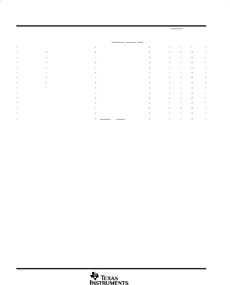
functional block diagram (pin numbers refer to 30-pin DB package)
|
|
TPS2216A |
|
|
9 |
|
|
|
|
AVCC |
|
|
|
|
|
|
|
|
15 |
|
|
|
10 |
3.3V |
S1 |
|
|
AVCC |
|
|
|
|
11 |
||
|
16 |
|
|
|
|
3.3V |
|
|
|
AVCC |
|
|
S2 |
|
|
|
|
|
17 |
|
|
|
|
3.3V |
CS |
|
|
|
|
|
|
|
|
||
|
|
S3 |
|
S7 |
8 |
|
|
|
|
||
|
|
|
|
AVPP |
|
|
|
CS |
|
|
|
|
|
|
|
|
|
|
|
|
|
S8 |
|
|
|
|
CS |
|
|
|
|
|
|
S9 |
|
|
|
|
CS |
|
|
|
|
|
|
S10 |
20 |
|
1 |
|
CS |
|
BVCC |
5V |
|
|
21 |
||
|
|
|
|
||
|
2 |
S4 |
|
|
BVCC |
5V |
|
|
22 |
||
|
|
|
|||
|
|
|
|
||
|
30 |
|
|
|
BVCC |
5V |
|
|
|
|
|
|
S5 |
|
|
|
|
|
|
|
|
|
|
|
|
CS |
|
|
|
|
|
S6 |
|
S11 |
23 |
|
|
|
|
||
|
|
CS |
|
|
BVPP |
|
|
|
|
|
|
|
|
|
|
S12 |
|
|
|
|
CS |
|
|
|
7 |
|
|
S13 |
|
12V² |
|
CS |
|
|
|
|
|
|
|
||
12V² |
24 |
|
|
S14 |
|
|
CS |
|
|
||
|
|
|
|
||
|
|
Internal |
|
|
|
|
|
Current Monitor |
|
|
|
|
29 |
MODE |
|
Thermal |
|
|
19 |
|
|
||
|
STBY |
|
|
|
|
|
3 |
|
|
|
|
|
DATA |
|
|
|
|
|
4 |
|
|
|
|
|
CLOCK |
|
|
|
|
|
5 |
|
|
|
|
|
LATCH |
|
|
|
|
|
6 |
|
|
|
|
|
RESET |
GND |
|
12 |
|
|
|
|
|
||
|
14 |
|
|
|
|
|
RESET |
|
|
|
|
|
18 |
|
|
|
|
|
OC |
|
|
|
|
|
|
|
|
|
|
² Both 12V pins must be connected together.
POST OFFICE BOX 655303 •DALLAS, TEXAS 75265 |
3 |
TPS2214A, TPS2216A
LOW-COST DUAL-SLOT PC CARD POWER SWITCH
FOR SERIAL PCMCIA CONTROLLERS
SLVS267 ± DECEMBER 1999
absolute maximum ratings over operating virtual free-air temperature (unless otherwise noted)²
Input voltage range for card power: VI(3.3V) . . . . . . . . . . . . . . . . . . . . . . . . . . . . . . |
. . . . . . . . . . . . . ±0.3 V to 6 V |
|
VI(5V) . . . . . . . . . . . . . . . . . . . . . . . . . . . . . . . |
. . . . . . . . . . . . . ±0.3 V to 6 V |
|
VI(12V) . . . . . . . . . . . . . . . . . . . . . . . . . . . . . . |
. . . . . . . . . . . . ±0.3 V to 14 |
V |
Logic input voltage . . . . . . . . . . . . . . . . . . . . . . . . . . . . . . . . . . . . . . . . . . . . . . . . . . . . |
. . . . . . . . . . . . . ±0.3 V to 6 |
V |
Output voltage range: VO(xVCC) . . . . . . . . . . . . . . . . . . . . . . . . . . . . . . . . . . . . . . |
. . . . . . . . . . . . . ±0.3 V to 6 |
V |
VO(xVPP) . . . . . . . . . . . . . . . . . . . . . . . . . . . . . . . . . . . . . . . |
. . . . . . . . . . . . ±0.3 V to 14 |
V |
Continuous total power dissipation . . . . . . . . . . . . . . . . . . . . . . . . . . . . . . . . . . . . . |
See Dissipation Rating Table |
|
Output current: IO(xVCC) . . . . . . . . . . . . . . . . . . . . . . . . . . . . . . . . . . . . . . . . . . . . . . |
. . . . . . . . . . . Internally limited |
|
IO(xVPP) . . . . . . . . . . . . . . . . . . . . . . . . . . . . . . . . . . . . . . . . . . . . . . . |
. . . . . . . . . . . Internally limited |
|
Operating virtual junction temperature range, TJ . . . . . . . . . . . . . . . . . . . . . . . . . . |
. . . . . . . . . . . ±40°C to 125°C |
|
Storage temperature range, Tstg . . . . . . . . . . . . . . . . . . . . . . . . . . . . . . . . . . . . . . . . |
. . . . . . . . . . . ±55°C to 150°C |
|
Lead temperature 1,6 mm (1/16 inch) from case for 10 seconds . . . . . . . . . . . . |
. . . . . . . . . . . . . . . . . . . 260°C |
|
²Stresses beyond those listed under ªabsolute maximum ratingsº may cause permanent damage to the device. These are stress ratings only, and functional operation of the device at these or any other conditions beyond those indicated under ªrecommended operating conditionsº is not implied. Exposure to absolute-maximum-rated conditions for extended periods may affect device reliability.
DISSIPATION RATING TABLE
|
T ≤ 25°C |
DERATING FACTOR³ |
T = 70°C |
T = 85°C |
|
PACKAGE |
A |
ABOVE TA = 25°C |
A |
A |
|
POWER RATING |
POWER RATING |
POWER RATING |
|||
|
|||||
DB |
1095 mW |
10.99 mW/°C |
602 mW |
438 mW |
|
|
|
|
|
|
|
DAP |
4255 mW |
42.55 mW/°C |
2340 mW |
1702 mW |
³ These devices are mounted on an JEDEC low-k board (2 oz. traces on surface), 1-W power applied.
recommended operating conditions
|
|
MIN |
MAX |
UNIT |
|
|
|
|
|
|
VI(3.3V) |
2.7 |
5.25 |
V |
Input voltage, VI |
VI(5V) |
2.7 |
5.25 |
V |
|
VI(12V) |
2.7 |
13.5 |
V |
Output current, IO |
IO(VCC) at TA = 70°C |
|
750 |
mA |
IO(VPP) at TA = 70°C |
|
200 |
mA |
|
|
|
|||
Clock frequency |
|
|
2.5 |
MHz |
|
|
|
|
|
|
Data |
200 |
|
|
Pulse duration |
|
|
|
ns |
Latch |
250 |
|
||
|
|
|
|
|
|
Clock |
100 |
|
|
|
|
|
|
|
Data hold time§ |
|
100 |
|
ns |
Data setup time§ |
|
100 |
|
ns |
Latch delay time§ |
|
100 |
|
ns |
Clock delay time§ |
|
250 |
|
ns |
Operating virtual junction temperature, TJ |
± 40 |
100 |
°C |
|
§ Refer to Figures 2 and 3. |
|
|
|
|
4 |
POST OFFICE BOX 655303 •DALLAS, TEXAS 75265 |
TPS2214A, TPS2216A
LOW-COST DUAL-SLOT PC CARD POWER SWITCH
FOR SERIAL PCMCIA CONTROLLERS
SLVS267 ± DECEMBER 1999
electrical characteristics, TJ = 25°C, VI(5V) = 5 V, VI(3.3V) = 3.3 V, VI(12V) = 12 V, STBY floating, all outputs unloaded (unless otherwise noted)
power switch
|
PARAMETER |
|
|
TEST CONDITIONS |
MIN TYP |
MAX |
UNIT |
||||||
|
|
|
|
|
|
|
|
|
|
|
|
|
|
|
|
3.3 V to xVCC, with one or |
TJ = 25°C, |
|
VI(5V) = 0 or 5, |
IO = 750 mA |
60 |
105 |
|
||||
|
|
two switches on |
|
TJ = 85°C, |
|
VI(5V) = 0 or 5, |
IO = 750 mA |
90 |
140 |
mΩ |
|||
|
|
5 V to xVCC, with one or |
TJ = 25°C, |
|
IO = 750 mA |
|
140 |
185 |
|||||
|
|
|
|
|
|||||||||
|
|
two switches on |
|
TJ = 85°C, |
|
IO = 750 mA |
|
160 |
200 |
|
|||
|
Switch resistance² |
3.3 V/5 V/12 V to xVPP |
TJ = 25°C, |
|
IO = 50 mA |
|
0.7 |
1.5 |
|
||||
|
TJ = 85°C, |
|
IO = 50 mA |
|
1.4 |
2.5 |
|
||||||
|
|
|
|
|
|
|
|||||||
|
|
3.3 V/5 V to xVCC |
|
TJ = 25°C, |
|
STBY |
= low, |
IO = 30 mA |
1.4 |
2 |
Ω |
||
|
|
|
TJ = 85°C, |
|
STBY = low, |
IO = 30 mA |
2 |
3 |
|||||
|
|
|
|
|
|
||||||||
|
|
3.3 V/5 V/12 V to xVPP |
TJ = 25°C, |
|
|
STBY |
= low, |
IO = 30 mA |
5 |
7 |
|
||
|
|
TJ = 85°C, |
|
STBY = low, |
IO = 30 mA |
10 |
16 |
|
|||||
|
|
|
|
|
|
||||||||
|
Clamp low voltage |
VO(xVCC) |
|
IO(xVCC) at 10 mA, After reset |
0.275 |
0.8 |
V |
||||||
|
VO(xVPP) |
|
IO(xVPP) at 10 mA, After reset |
0.275 |
0.8 |
||||||||
|
|
|
|
||||||||||
|
|
IO(xVCC) high-impedance |
TJ = 25°C |
|
|
|
|
|
|
1 |
10 |
|
|
Ilkg |
Leakage current |
state |
|
TJ = 85°C |
|
|
|
|
|
|
2 |
50 |
A |
IO(xVPP) high-impedance |
TJ = 25°C |
|
|
|
|
|
|
1 |
10 |
||||
|
|
|
|
|
|
|
|
|
|||||
|
|
state |
|
TJ = 85°C |
|
|
|
|
|
|
2 |
50 |
|
|
|
IO(xVCC) |
|
TJ = 85°C, |
|
|
|
|
|
|
1 |
2.5 |
A |
|
Short-circuit output |
IO(xVPP) |
|
Output powered into a short to GND |
250 |
500 |
mA |
||||||
IOS |
|
|
TJ = 85°C, |
|
|
|
|
|
|
|
|
|
|
current limit² |
Standby mode, IO(xVCC) |
|
|
|
|
|
|
35 |
65 |
|
|||
|
|
|
|
Output powered into a short to GND, |
|
|
mA |
||||||
|
|
Standby mode, IO(xVPP) |
30 |
60 |
|||||||||
|
|
STBY = 0 V |
|
|
|
|
|
|
|
||||
|
Current limit |
xVCC switch |
|
100-mΩ short circuit |
|
100 |
|
s |
|||||
|
response time³ |
|
|
|
|
|
|||||||
|
xVPP switch |
|
|
16 |
|
||||||||
|
|
|
|
|
|
|
|
|
|
|
|||
|
|
|
II(3.3V) |
|
|
|
|
|
|
|
0.01 |
2 |
|
|
|
Normal operation |
II(5V) |
VO(xVCC) = VO(xVPP) = 5 V |
100 |
120 |
A |
||||||
|
|
II(12V) |
|
|
|
|
|
|
|
6 |
10 |
|
|
|
|
and in reset |
|
|
|
|
|
|
|
|
|||
|
|
II(3.3V) |
|
|
|
|
|
|
|
100 |
120 |
|
|
II |
Input current§ |
mode |
VI(5V) = 0, |
|
|
VO(xVCC) = |
3.3 V, |
A |
|||||
|
II(5V) |
|
|
0 |
|
||||||||
|
VO(xVPP) = 12 V |
|
|
||||||||||
|
|
|
II(12V) |
|
22 |
30 |
|
||||||
|
|
|
|
|
|
|
|
|
|
|
|||
|
|
|
II(3.3V) |
|
|
|
|
|
|
|
|
1 |
|
|
|
Shutdown mode |
II(5V) |
VO(xVCC) = Hi-Z, VO(xVPP) = Hi-Z |
|
1 |
A |
||||||
|
|
|
II(12V) |
|
|
|
|
|
|
|
|
1 |
|
|
Thermal shutdown³ |
Trip point, TJ |
|
|
|
|
|
|
|
|
155 |
|
°C |
|
Hysteresis |
|
|
|
|
|
|
|
|
10 |
|
||
|
|
|
|
|
|
|
|
|
|
|
|
||
² Pulse-testing techniques maintain junction temperature close to ambient temperature (250- s-wide pulse, less than 0.5% duty cycle); thermal effects must be taken into account separately.
³ Specified by design, not tested in production.
§ Input currents do not include logic input currents (presented in electrical characteristics for logic section); clock is inactive. NOTE: VI(3.3V) or VI(5V) must be biased for switches to function.
POST OFFICE BOX 655303 •DALLAS, TEXAS 75265 |
5 |
TPS2214A, TPS2216A
LOW-COST DUAL-SLOT PC CARD POWER SWITCH
FOR SERIAL PCMCIA CONTROLLERS
SLVS267 ± DECEMBER 1999
electrical characteristics, TJ = 25°C, VI(5V) = 5 V, VI(3.3V) = 3.3 V, VI(12V) = 12 V, STBY floating, all outputs unloaded (unless otherwise noted) (continued)
logic section (CLOCK, DATA, LATCH, MODE, RESET, RESET, STBY, OC)
|
PARAMETER |
|
|
TEST CONDITIONS |
MIN |
TYP |
MAX |
UNIT |
||||||||||||
|
|
|
|
|
|
|
|
|
|
|
|
|
|
|
|
|
|
|
||
|
II(RESET) or I |
|
² |
VI(RESET) = 5 V or V |
I(RESET) |
= 0 V |
|
30 |
50 |
|
||||||||||
|
I(RESET) |
|
|
|
|
|
|
|
||||||||||||
|
VI(RESET) = 0 V or V |
|
= 5 V |
|
|
1 |
|
|||||||||||||
|
I(RESET) |
|
|
|
||||||||||||||||
|
II(MODE)² |
VI(MODE) = 5 V |
|
|
|
|
30 |
50 |
|
|||||||||||
Logic input current |
VI(MODE) = 0 V |
|
|
|
|
|
1 |
µA |
||||||||||||
|
|
|
|
|
|
|
|
|
|
|
|
|||||||||
|
|
|
|
|
|
|
|
|
|
|
|
|
|
|
|
|
|
|||
|
|
|
|
|
|
|
|
|
|
V |
I(STBY) |
= 5 V |
|
|
|
|
|
1 |
|
|
|
II(STBY)² |
|
|
|
|
|
|
|||||||||||||
|
|
|
|
|
|
|
|
|
|
|
|
|||||||||
|
VI(STBY) = 0 V |
|
|
|
|
30 |
50 |
|
||||||||||||
|
|
|
|
|
|
|
|
|
|
|
|
|
|
|
||||||
|
II(CLOCK) or II(DATA) or II(LATCH) |
|
|
|
|
|
|
|
|
|
1 |
|
||||||||
Logic input high level |
VI(5V) = 5 V |
|
|
|
2 |
|
|
V |
||||||||||||
VI(5V) = 0 |
V |
|
|
|
2 |
|
|
|||||||||||||
|
|
|
|
|
|
|
|
|
|
|
|
|
|
|
|
|||||
Logic input low level |
|
|
|
|
|
|
|
|
|
0.8 |
V |
|||||||||
|
|
|
|
|
|
|
|
|
|
|
|
|
|
|
|
|
||||
|
|
|
|
|
|
|
|
|
|
VI(5V) = 5 |
V, |
IO = 1 mA |
VI(5V)±0.4 |
|
|
V |
||||
Logic output high level, OC |
|
|
||||||||||||||||||
VI(5V) = 0 |
V, |
IO = 1 mA |
VI(3.3V)±0.4 |
|
|
|||||||||||||||
|
|
|
|
|
|
|
|
|
|
|
|
|
||||||||
Logic output low level, |
|
|
|
|
|
|
|
|
IO = 1 mA |
|
|
|
|
|
|
0.4 |
V |
|||
OC |
|
|
|
|
|
|
|
|||||||||||||
² RESET and MODE have internal 150-kΩ pulldown resistors; RESET and STBY have internal 150-kΩ pullup resistors.
6 |
POST OFFICE BOX 655303 •DALLAS, TEXAS 75265 |
TPS2214A, TPS2216A
LOW-COST DUAL-SLOT PC CARD POWER SWITCH
FOR SERIAL PCMCIA CONTROLLERS
|
|
|
|
|
|
|
|
|
SLVS267 ± DECEMBER 1999 |
|
|
|
|
|
|
|
|
|
|
|
|
||
switching characteristics |
|
|
|
|
|
|
|
|
|||
|
|
|
|
|
|
|
|
|
|||
|
|
PARAMETER² |
LOAD CONDITION² |
TEST CONDITIONS² |
MIN TYP MAX |
UNIT |
|
||||
|
|
|
CL(xVCC) = 0.1 F, |
VO(xVCC) |
|
|
1 |
|
|
||
|
|
|
CL(xVPP) = 0.1 F, |
|
|
|
|
|
|
||
|
|
|
IO(xVCC) = 0§, |
|
VO(xVPP) |
|
|
0.8 |
|
|
|
|
|
|
I |
= 0§ |
|
|
|
|
|
||
t |
r |
Output rise times³ |
O(xVPP) |
|
|
|
|
|
|
ms |
|
CL(xVCC) = 150 |
F, |
VO(xVCC) |
|
|
1.2 |
|
|||||
|
|
|
|
|
|
||||||
|
|
|
|
|
|
|
|||||
|
|
|
CL(xVPP) = 10 F, |
|
|
|
|
|
|
||
|
|
|
IO(xVCC) = 1 A, |
|
VO(xVPP) |
|
|
2.5 |
|
|
|
|
|
|
IO(xVPP) = 50 mA |
|
|
|
|
||||
|
|
|
|
|
|
|
|
|
|||
|
|
|
CL(xVCC) = 0.1 F, |
VO(xVCC) |
|
|
0.01 |
|
|
||
|
|
|
CL(xVPP) = 0.1 F, |
|
|
|
|
|
|
||
|
|
|
IO(xVCC) = 0§, |
|
VO(xVPP) |
|
|
0.01 |
|
|
|
|
|
|
I |
= 0§ |
|
|
|
|
|
||
t |
f |
Output fall times³ |
O(xVPP) |
|
|
|
|
|
|
ms |
|
CL(xVCC) = 150 |
F, |
VO(xVCC) |
|
|
3 |
|
|||||
|
|
|
|
|
|
||||||
|
|
|
|
|
|
|
|||||
|
|
|
CL(xVPP) = 10 F, |
|
|
|
|
|
|
||
|
|
|
IO(xVCC) = 1 A, |
|
VO(xVPP) |
|
|
8 |
|
|
|
|
|
|
IO(xVPP) = 50 mA |
|
|
|
|
||||
|
|
|
|
|
|
|
|
|
|||
|
|
|
|
|
|
Latch↑ to xVPP (12 V) |
|
tpd(on) |
3 |
|
|
|
|
|
|
|
|
|
tpd(off) |
25 |
|
|
|
|
|
|
|
|
|
|
|
|
|
||
|
|
|
|
|
|
Latch↑ to xVPP (5 V) |
|
tpd(on) |
0.6 |
|
|
|
|
|
|
|
|
|
tpd(off) |
8.5 |
|
|
|
|
|
|
|
|
|
|
|
|
|
||
|
|
|
|
|
|
Latch↑ to xVPP (3.3 V), VI(5V) |
= 5 V |
tpd(on) |
0.6 |
|
|
|
|
|
|
|
|
tpd(off) |
9 |
|
|
||
|
|
|
|
|
|
|
|
|
|||
|
|
|
CL(xVCC) = 0.1 |
F, |
|
|
|
|
|
|
|
|
|
|
|
|
tpd(on) |
1.4 |
|
|
|||
|
|
|
CL(xVPP) = 0.1 F, |
Latch↑ to xVPP (3.3 V), VI(5V) |
= 0 V |
|
|
||||
|
|
|
|
§ |
|
t |
9 |
|
|
||
|
|
|
IO(xVCC) = 0 , |
|
|
|
|
|
|||
|
|
|
I |
= 0§ |
|
|
|
pd(off) |
|
|
|
|
|
|
|
|
|
|
|
|
|
||
|
|
|
O(xVPP) |
|
|
|
|
tpd(on) |
0.3 |
|
|
|
|
|
|
|
|
Latch↑ to xVCC (5 V) |
|
|
|
||
|
|
|
|
|
|
|
tpd(off) |
15 |
|
|
|
|
|
|
|
|
|
|
|
|
|
||
|
|
|
|
|
|
Latch↑ to xVCC (3.3 V), VI(5V) |
= 5 V |
tpd(on) |
0.2 |
|
|
|
|
|
|
|
|
tpd(off) |
15 |
|
|
||
|
|
|
|
|
|
|
|
|
|
||
|
|
|
|
|
|
Latch↑ to xVCC (3.3 V), VI(5V) |
= 0 V |
tpd(on) |
0.4 |
|
|
t |
pd |
Propagation delay³ |
|
|
|
tpd(off) |
15 |
ms |
|
||
|
|
|
|
|
|
||||||
|
|
|
|
|
tpd(on) |
4.5 |
|
||||
|
|
|
|
|
|
|
|
|
|||
|
|
|
|
|
|
Latch↑ to xVPP (12 V) |
|
|
|
||
|
|
|
|
|
|
|
tpd(off) |
13 |
|
|
|
|
|
|
|
|
|
|
|
|
|
||
|
|
|
|
|
|
Latch↑ to xVPP (5 V) |
|
tpd(on) |
3.3 |
|
|
|
|
|
|
|
|
|
tpd(off) |
8 |
|
|
|
|
|
|
|
|
|
|
|
|
|
||
|
|
|
|
|
|
Latch↑ to xVPP (3.3 V), VI(5V) |
= 5 V |
tpd(on) |
3 |
|
|
|
|
|
|
|
|
tpd(off) |
9 |
|
|
||
|
|
|
|
|
|
|
|
|
|||
|
|
|
CL(xVCC) = 150 |
F, |
|
|
|
|
|
|
|
|
|
|
|
|
tpd(on) |
3 |
|
|
|||
|
|
|
CL(xVPP) = 10 F, |
Latch↑ to xVPP (3.3 V), VI(5V) = 0 V |
|
|
|||||
|
|
|
IO(xVCC) = 1 A, |
|
t |
9 |
|
|
|||
|
|
|
IO(xVPP) = 50 mA |
|
|
pd(off) |
|
|
|
||
|
|
|
Latch↑ to xVCC (5 V) |
|
tpd(on) |
1 |
|
|
|||
|
|
|
|
|
|
|
|
|
|||
|
|
|
|
|
|
|
tpd(off) |
12 |
|
|
|
|
|
|
|
|
|
|
|
|
|
||
|
|
|
|
|
|
Latch↑ to xVCC (3.3 V), VI(5V) |
= 5 V |
tpd(on) |
0.6 |
|
|
|
|
|
|
|
|
tpd(off) |
12 |
|
|
||
|
|
|
|
|
|
|
|
|
|
||
|
|
|
|
|
|
Latch↑ to xVCC (3.3 V), VI(5V) |
= 0 V |
tpd(on) |
1 |
|
|
|
|
|
|
|
|
tpd(off) |
12 |
|
|
||
|
|
|
|
|
|
|
|
|
|
||
² Refer to Parameter Measurement Information
³ Specified by design: not tested in production.
§ No card inserted, assumes 0.1- F recommended output capacitor (see Figure 32).
POST OFFICE BOX 655303 •DALLAS, TEXAS 75265 |
7 |
TPS2214A, TPS2216A
LOW-COST DUAL-SLOT PC CARD POWER SWITCH
FOR SERIAL PCMCIA CONTROLLERS
SLVS267 ± DECEMBER 1999
PARAMETER MEASUREMENT INFORMATION
|
xVPP |
|
xVCC |
|
||
|
|
IO(xVPP) |
|
I |
|
|
|
|
|
|
O(xVCC) |
||
|
|
|
LOAD CIRCUITS |
|
|
|
LATCH |
50% |
VDD |
LATCH |
50% |
VDD |
|
GND |
GND |
|||||
|
|
|
|
|||
tpd(on) |
tpd(off) |
|
tpd(on) |
tpd(off) |
|
|
|
|
|
|
|||
VO(xVPP) |
90% |
GND |
VO(xVCC) |
90% |
GND |
|
|
10% |
|
10% |
|||
|
|
|
|
|||
|
Propagation Delay (xVPP) |
|
Propagation Delay (xVCC) |
|||
tr |
tf |
|
tr |
tf |
|
|
|
|
|
|
|||
VO(xVPP) |
90% |
GND |
VO(xVCC) |
90% |
GND |
|
|
10% |
|
10% |
|||
|
|
|
|
|||
|
Rise/Fall Time (xVPP) |
|
|
Rise/Fall Time (xVCC) |
|
|
LATCH |
50% |
VDD |
|
50% |
VDD |
|
GND |
|
GND |
||||
|
|
|
|
|||
ton |
toff |
|
ton |
toff |
|
|
|
|
|
|
|||
VO(xVPP) |
90% |
|
VO(xVCC) |
90% |
|
|
|
10% |
GND |
|
10% |
GND |
|
|
|
|
|
|||
|
Turn On/Off Time (xVPP) |
|
Turn On/Off Time (xVCC) |
|
||
|
|
|
VOLTAGE WAVEFORMS |
|
|
|
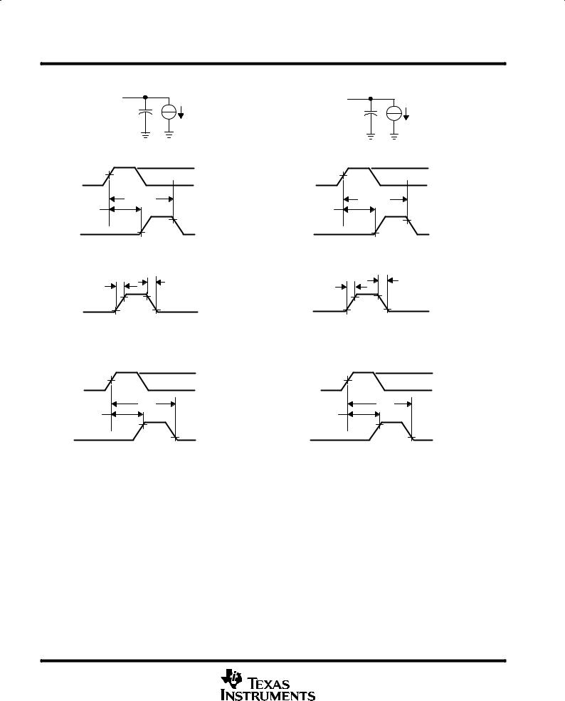
Figure 1. Test Circuits and Voltage Waveforms
8 |
POST OFFICE BOX 655303 •DALLAS, TEXAS 75265 |
TPS2214A, TPS2216A
LOW-COST DUAL-SLOT PC CARD POWER SWITCH
FOR SERIAL PCMCIA CONTROLLERS
SLVS267 ± DECEMBER 1999
PARAMETER MEASUREMENT INFORMATION
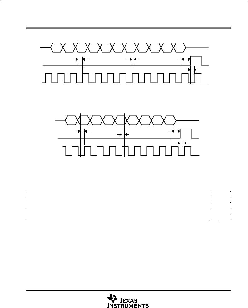
DATA |
D10 |
D9 |
D8 |
D7 |
D6 |
D5 |
D4 |
D3 |
D2 |
D1 |
D0 |
|
Data Setup Time |
|
|
Data Hold Time |
|
|
Latch Delay Time |
|
|||
LATCH |
|
|
|
|
|
|
|
|
|
|
|
Clock Delay Time
CLOCK
NOTE: Data is clocked in on the positive edge of the clock. The positive edge of the latch signal should occur before the next positive edge of the clock. For definition of D0 to D10, see the control logic table.
Figure 2. Serial-Interface Timing for Independent xVPP Switching When MODE = 5 V or 3.3 V
DATA |
D8 |
D7 |
D6 |
D5 |
D4 |
D3 |
D2 |
D1 |
D0 |
Data Setup Time |
|
Data Hold Time |
|
|
Latch Delay Time |
|
|||
|
|
|
|
|
|
|
|
||
LATCH |
|
|
|
|
|
|
|
|
|
Clock Delay Time
CLOCK
NOTE: Data is clocked in on the positive edge of the clock. The positive edge of the latch signal should occur before the next positive edge of the clock. For definition of D0 to D8, see the control logic table.
Figure 3. Serial-Interface Timing When MODE = 0 V or Floating
Table of Timing Diagrams²
|
|
|
FIGURE |
|
|
|
|
|
Short-circuit current response, short applied to powered-on 5-V xVCC switch output |
4 |
|
|
|
|
|
|
Short-circuit current response, short applied to powered-on 12-V xVPP switch output |
5 |
|
|
|
|
|
|
|
response with ramped load on 5-V xVCC switch output |
6 |
|
OC |
||
|
|
|
|
|
|
response with ramped load on 12-V xVPP switch output |
7 |
|
OC |
||
|
|
|
|
² Timing tests are conducted at free-air temperature, VI(5V) = 5 V, VI(3.3V) = 3.3 V, VI(12V) = 12 V, CL = 0.1 F on each output, STBY floating.
POST OFFICE BOX 655303 •DALLAS, TEXAS 75265 |
9 |
 Loading...