


TPS3705-30
TEXAS INSTRUMENTS TPS3705-30, TPS3705-33, TPS3705-50, TPS3707-25, TPS3707-30 Technical data
...
TPS3705-30, TPS3705-33, TPS3705-50
TPS3707-25, TPS3707-30, TPS3707-33, TPS3707-50
PROCESSOR SUPERVISORY CIRCUITS WITH POWER-FAIL
SLVS184B – NOVEMBER 1998 – REVISED JANUAR Y 1999
features
D
Power-On Reset Generator with Fixed
Delay Time of 200 ms, no External
Capacitor Needed
D
Precision Supply Voltage Monitor 2.5 V, 3 V,
3.3 V, and 5 V
D
Pin-For-Pin Compatible with the MAX705
through MAX708 Series
D
Integrated Watchdog Timer (TPS3705 only)
D
Voltage Monitor for Power-Fail or
Low-Battery Warning
D
Maximum Supply Current of 50 µA
D
MSOP-8 and SO-8 Packages
D
T emperature Range...–40°C to 85°C
typical applications
D
Designs Using DSPs, Microcontrollers or
Microprocessors
D
Industrial Equipment
D
Programmable Controls
D
Automotive Systems
D
Portable/Battery Powered Equipment
D
Intelligent Instruments
D
Wireless Communication Systems
D
Notebook/Desktop Computers
TPS3705 ...D PACKAGE
(TOP VIEW)
MR
1
V
GND
V
GND
NC – No internal connection
TPS3705 . . . DGN PACKAGE
RESET
WDO
V
TPS3707 . . . DGN PACKAGE
RESET
RESET
5 V12 V
V
2
DD
3
4
PFI
TPS3707 ...D PACKAGE
(TOP VIEW)
MR
1
2
DD
3
4
PFI
(TOP VIEW)
1
2
MR
3
4
DD
(TOP VIEW)
1
2
MR
3
4
DD
8
7
6
5
8
7
6
5
8
7
6
5
8
7
6
5
WDO
RESET
WDI
PFO
RESET
RESET
NC
PFO
WDI
PFO
PFI
GND
NC
PFO
PFI
GND
V
DD
PFO
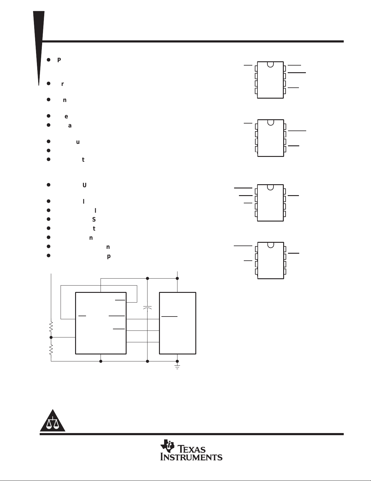
910 kΩ
120 kΩ
TPS3705–50
MR RESET
PFI
GND
100 nF
WDO
WDI
Figure 1. Typical MSP430 Application
Please be aware that an important notice concerning availability, standard warranty, and use in critical applications of
Texas Instruments semiconductor products and disclaimers thereto appears at the end of this data sheet.
PRODUCTION DATA information is current as of publication date.
Products conform to specifications per the terms of Texas Instruments
standard warranty. Production processing does not necessarily include
testing of all parameters.
V
DD
MSP430P112
RESET/NMI
I/O
I/O
GND
NC – No internal connection
Copyright 1999, Texas Instruments Incorporated
POST OFFICE BOX 655303 • DALLAS, TEXAS 75265
1
TPS3705-30, TPS3705-33, TPS3705-50
TPS3707-25, TPS3707-30, TPS3707-33, TPS3707-50
PROCESSOR SUPERVISORY CIRCUITS WITH POWER-FAIL
SLVS184B – NOVEMBER 1998 – REVISED JANUAR Y 1999
description
The TPS3705, TPS3707 family of microprocessor supply-voltage supervisors provide circuit initialization and
timing supervision, primarily for DSP and processor-based systems.
During power-on, RESET
supply voltage supervisor monitors V
voltage V
. An internal timer delays the return of the output to the inactive state (high) to ensure proper system
IT+
reset. The delay time, t
voltage drops below the threshold voltage V
is asserted when the supply voltage V
and keeps RESET active as long as VDD remains below the threshold
DD
= 200 ms, starts after V
d typ
IT–
has risen above the threshold voltage V
DD
, the output becomes active (low) again. No external components
are required. All the devices of this family have a fixed-sense threshold voltage V
becomes higher than 1.1 V . Thereafter , the
DD
. When the supply
IT+
set by an internal voltage
IT–
divider.
The TPS3705-xx and TPS3707-xx devices incorporate a manual reset input, MR
RESET
to become active.
. A low level at MR causes
The TPS370x-xx families integrate a power-fail comparator which can be used for low-battery detection,
power-fail warning, or for monitoring a power supply other than the main supply.
The TPS3705-xx devices have a watchdog timer that is periodically triggered by a positive or negative transition
at WDI. When the supervising system fails to retrigger the watchdog circuit within the time-out interval,
t
= 1.6 s, WDO becomes active. This event also reinitializes the watchdog timer. Leaving WDI unconnected
t(out)
disables the watchdog.
The TPS3707-xx devices do not have the Watchdog function, but include a high-level output RESET.
The product spectrum is designed for supply voltages of 2.5 V , 3 V, 3.3 V, and 5 V . The circuits are available in
either 8-pin MSOP or standard SOIC packages. The TPS3705, TPS3707 devices are characterized for
operation over a temperature range of –40°C to 85°C.
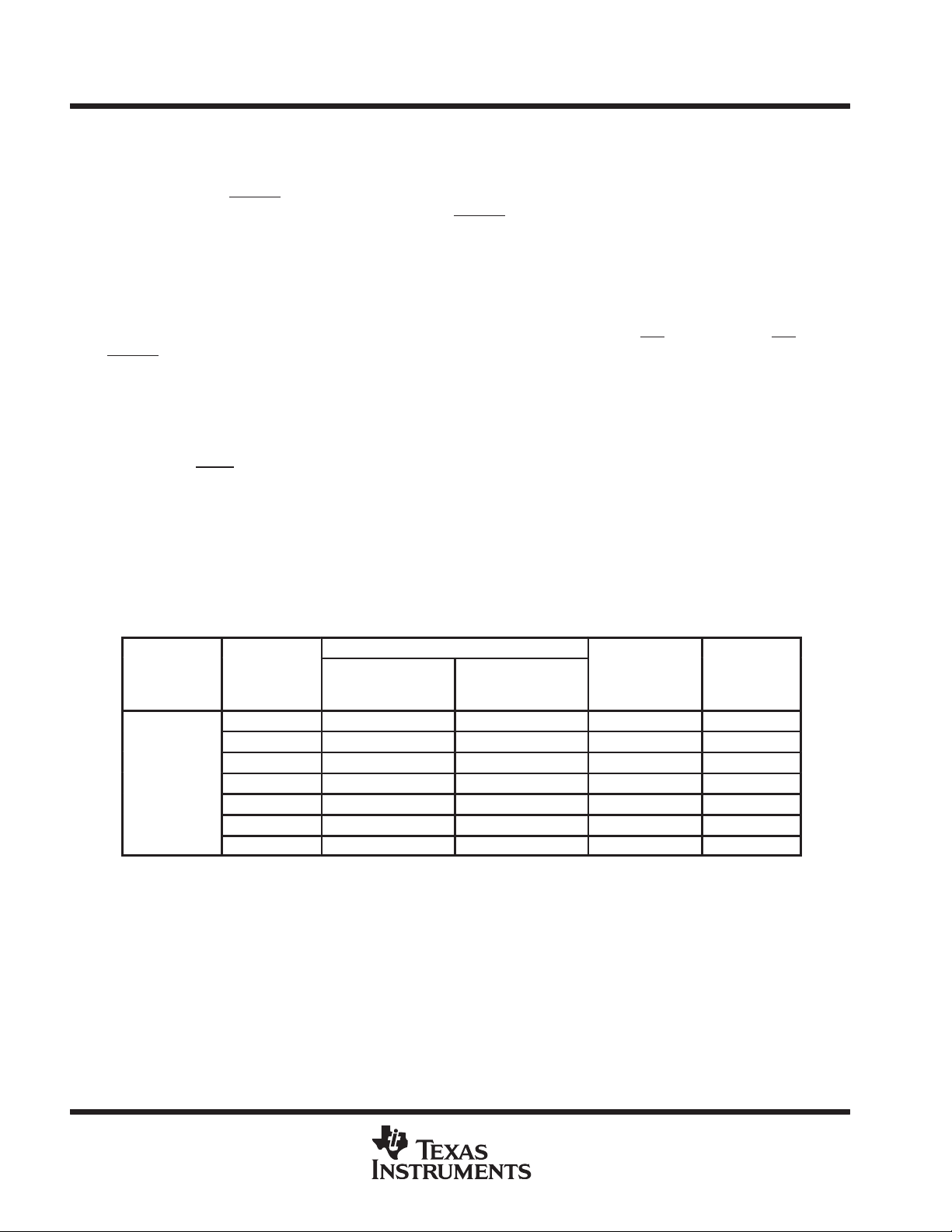
AVAILABLE OPTIONS
PACKAGED DEVICES
T
A
–40°C to 85°C
THRESHOLD
VOLTAGE
2.63 V TPS3705–30D TPS3705–30DGN TIAAT TPS3705-30Y
2.93 V TPS3705–33D TPS3705–33DGN TIAAU TPS3705–33Y
4.55 V TPS3705–50D TPS3705–50DGN TIAAV TPS3705–50Y
2.25 V TPS3707–25D TPS3707–25DGN TIAAW TPS3707–25Y
2.63 V TPS3707–30D TPS3707–30DGN TIAAX TPS3707–30Y
2.93 V TPS3707–33D TPS3707–33DGN TIAAY TPS3707–33Y
4.55 V TPS3707–50D TPS3707–50DGN TIAAZ TPS3707–50Y
SMALL OUTLINE
(D)
POWER–PAD
µ-SMALL OUTLINE
(DGN)
MARKING DGN
PACKAGE
CHIP FORM
(Y)
2
POST OFFICE BOX 655303 • DALLAS, TEXAS 75265
TPS3705-30, TPS3705-33, TPS3705-50
TPS3707-25, TPS3707-30, TPS3707-33, TPS3707-50
PROCESSOR SUPERVISORY CIRCUITS WITH POWER-FAIL
SLVS184B – NOVEMBER 1998 – REVISED JANUAR Y 1999
Function Tables
TRUTH TABLE, TPS3705
VDD>V
MR
H→L 1 H→L 30 ns
L→H 1L→H200 ms
H 1→0H→L 3 µs
H 0→1 L→H 200 ms
TRUTH TABLE, TPS3707
MR
H→L 1 H→L L→H 30 ns
L→H 1L→HH→L 200 ms
VDD>V
IT
H 1→0H→LL→H3 µs
H0→1L→HH→L200 ms
TRUTH TABLE, TPS370x
PFI>V
IT
0→1 L→H 0.5 µs
1→0 H→L 0.5 µs
IT
RESET
PFO
RESET
TYPICAL
DELAY
RESET
TYPICAL
DELAY
TYPICAL
DELAY
functional block diagram
V
DD
MR
GND
PFI
WDI
14 kΩ
R1
R2
Reference
Voltage
of 1.25 V
Transition
Detection
+
_
_
+
TPS3705
TPS3707
Reset
Logic + Timer
Oscillator
Watchdog
Logic + Timer
RESET
RESET
Only
TPS3707
PFO
WDO
Only
TPS3705
40 kΩ
POST OFFICE BOX 655303 • DALLAS, TEXAS 75265
Only
TPS3705
3
TPS3705-30, TPS3705-33, TPS3705-50
TPS3707-25, TPS3707-30, TPS3707-33, TPS3707-50
PROCESSOR SUPERVISORY CIRCUITS WITH POWER-FAIL
SLVS184B – NOVEMBER 1998 – REVISED JANUAR Y 1999
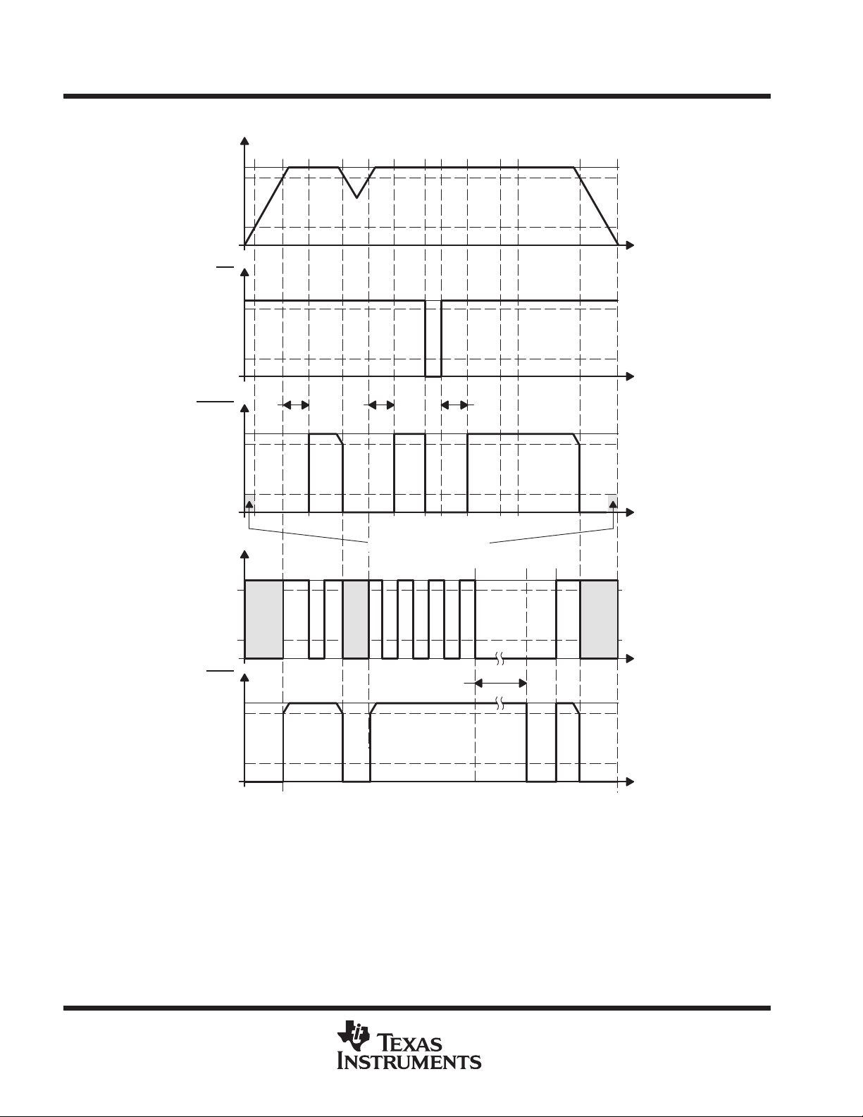
timing diagrams
V
DD
5 V
4.5 V
1.1 V
0 V
MR
5 V
4.5 V
1.1 V
0 V
t
t
RESET
5 V
4.5 V
1.1 V
0 V
WDI
5 V
4.5 V
1.1 V
0 V
WDO
5 V
4.5 V
1.1 V
0 V
t
d
Don’t Care
t
d
Undefined Behavior
Don’t Care
t
t(out)
t
d
t
Don’t Care
t
t
4
POST OFFICE BOX 655303 • DALLAS, TEXAS 75265
I/O
DESCRIPTION
6
8
TPS3705-30, TPS3705-33, TPS3705-50
TPS3707-25, TPS3707-30, TPS3707-33, TPS3707-50
PROCESSOR SUPERVISORY CIRCUITS WITH POWER-FAIL
SLVS184B – NOVEMBER 1998 – REVISED JANUAR Y 1999
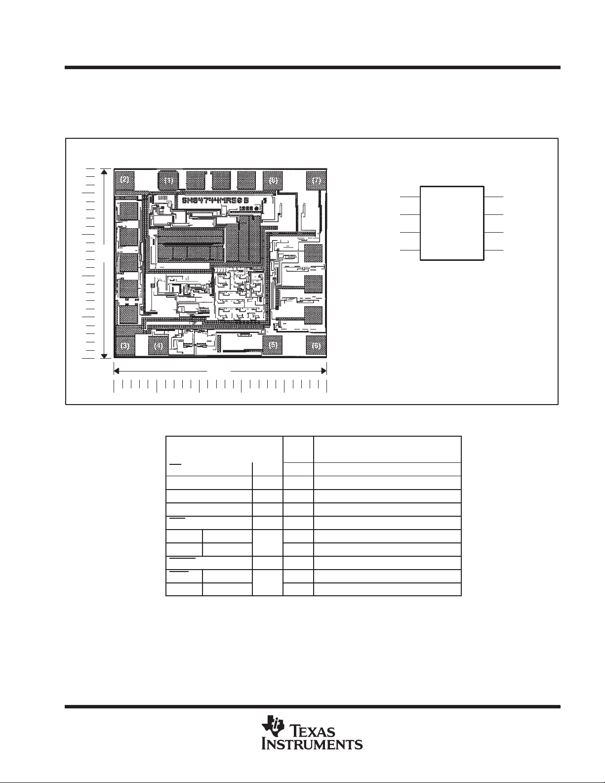
TPS370xY chip information
These chips, when properly assembled, display characteristics similar to those of the TPS370x. Thermal
compression or ultrasonic bonding may be caused on the doped-aluminum bonding pads. The chips may be
mounted with conductive epoxy or a gold-silicon preform.
BONDING PAD ASSIGNMENTS
46
(1)
(2)
(3)
(4)
CHIP THICKNESS: 10 MILS TYPICAL
BONDING PADS: 4 × 4 MINIMUM
TJ max = 150°C
TOLERANCES ARE ±10%
ALL DIMENSIONS ARE IN MILS
50
Terminal Functions
TERMINAL
NAME NO.
MR 1 I Manual reset
VDD 2 Supply voltage
GND 3 Ground
PFI 4 I Power-fail comparator input
PFO 5 O Power-fail comparator output
WDI TPS3705
NC TPS3707
RESET 7 O Active-low reset output
WDO TPS3705
RESET TPS3707
I Watchdog timer input
No internal connection
O Watchdog timer output
O Active-high reset output
TPS3705Y
TPS3707Y
(8)
(7)
(6)
(5)
POST OFFICE BOX 655303 • DALLAS, TEXAS 75265
5
 Loading...