


Texas Instruments TPS60131PWPR, TPS60132PWP, TPS60131PWP, TPS60130PWPR, TPS60130PWP Datasheet
...TPS60130, TPS60131, TPS60132, TPS60133 REGULATED 5-V, 300 mA HIGH EFFICIENCY CHARGE PUMP DC/DC CONVERTERS
SLVS258A ± NOVEMBER 1999 ± REVISED DECEMBER 1999
features
DUp to 90% Efficiency From 2.7-V to 5.4-V Input Voltage Range Because of Special Switching Topology
DUp to 300-mA Output Current (TPS60130 and TPS60131)
DNo Inductors Required, Low EMI
DRegulated 5-V ±4% Output
DOnly Four External Components Required
D60- A Quiescent Supply Current
D0.05- A Shutdown Current
DLoad Disconnected in Shutdown
DSpace-Saving, Thermally-Enhanced PowerPADt Package
DEvaluation Module Available (TPS60130EVM±143)
description
applications
DBattery-Powered Applications
DThree Battery Cells to 5-V Conversion or Point-of-Use 3.3 V to 5-V Conversion
DLilon Battery to 5-V Conversion
DPortable Instruments
DBattery-Powered Microprocessor Systems
DBackup-Battery Boost Converters
DPDA's, Organizers, Laptops
DHandheld Instrumentation
DMedical Instruments (e.g., Glucose Meters)
DPCMCIA and 5-V Smart Card Supply
The TPS6013x step-up, regulated charge pumps generate a 5-V ±4% output voltage from a 2.7-V to 5.4-V input voltage (three alkaline, NiCd, or NiMH batteries or one Lithium or Lilon battery). The output current is 300 mA for the TPS60130/ TPS60131 and 150 mA for the TPS60132/ TPS60133, all from a 3-V input. Only four external capacitors are needed to build a complete high efficiency dc/dc charge pump converter. To achieve the high efficiency over a wide input voltage range, the charge pump automatically selects between a 1.5x or doubler conversion mode. From a 3-V input, all ICs can start with full load current.
efficiency (TPS60130, TPS60131) |
|
|
||||||
|
100 |
|
|
IO = 66 mA |
|
|
|
|
|
|
|
|
|
|
|
||
|
90 |
|
|
|
|
|
|
|
|
80 |
|
|
|
|
IO = 216 mA |
|
|
|
|
|
|
|
|
|
|
|
|
70 |
|
|
|
|
|
|
|
± % |
60 |
IO = 108 mA |
IO = 300 mA |
|
|
|||
|
|
|
|
|||||
|
|
|
|
|
||||
Efficiency |
50 |
|
|
|
|
|
|
|
40 |
|
|
|
|
|
|
|
|
|
|
|
|
|
|
|
|
|
|
30 |
|
|
|
|
|
|
|
|
20 |
|
|
|
|
|
|
|
|
10 |
|
|
|
|
|
|
|
|
0 |
|
|
|
|
4.6 |
5 |
5.4 |
|
2.6 |
3 |
3.4 |
3.8 |
4.2 |
|||
|
|
|
VI ± Input Voltage ± V |
|
|
|||
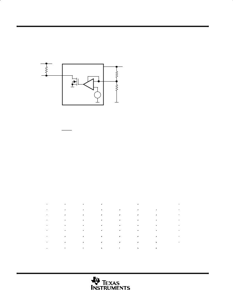
typical operating circuit
Input |
|
TPS60130 |
Output |
|
||
2.7 V to 5.4 V |
5 V, 300 mA |
|||||
|
|
|||||
|
|
IN |
OUT |
|
|
|
Ci |
R1 |
IN |
OUT |
Co |
|
|
15 F |
|
|
|
33 |
|
|
|
|
LBI |
FB |
F |
||
|
|
R3 |
|
|||
|
R2 |
|
LBO |
|
|
|
|
|
|
|
|
||
|
C1 |
C1+ |
C2+ |
|
|
|
|
|
|
C2 |
|
||
|
2.2 F |
C1± |
C2± |
|
||
|
2.2 F |
|
||||
|
|
ENABLE |
|
|
|
|
|
OFF/ON |
PGND GND |
|
|
||
Please be aware that an important notice concerning availability, standard warranty, and use in critical applications of Texas Instruments semiconductor products and disclaimers thereto appears at the end of this data sheet.
PowerPAD is a trademark of Texas Instruments Incorporated.
PRODUCTION DATA information is current as of publication date. Products conform to specifications per the terms of Texas Instruments standard warranty. Production processing does not necessarily include testing of all parameters.
Copyright 1999, Texas Instruments Incorporated
POST OFFICE BOX 655303 •DALLAS, TEXAS 75265 |
1 |

TPS60130, TPS60131, TPS60132, TPS60133
REGULATED 5-V, 300 mA HIGH EFFICIENCY CHARGE PUMP
DC/DC CONVERTERS
SLVS258A ± NOVEMBER 1999 ± REVISED DECEMBER 1999
description (continued)
The devices feature the power-saving pulse-skip mode to extend battery life at light loads. TPS60130 and TPS60132 include a low-battery comparator; TPS60131 and TPS60133 feature a power-good output. The logic shut-down function reduces the supply current to 1 A (max) and disconnects the load from the input. Special current-control circuitry prevents excessive current from being drawn from the battery during startup. This dc/dc converter requires no inductors and therefore EMI is of low concern. It is available in the small, thermally enhanced 20-pin PowerPADt package (PWP).
|
|
|
|
PWP PACKAGE |
|
|
|
|
|
|
PWP PACKAGE |
|
|
|
||||
|
|
|
(TPS60130/TPS60132) |
|
|
|
|
|
|
(TPS60131/TPS60133) |
|
|
|
|||||
|
|
|
|
|
(TOP VIEW) |
|
|
|
|
|
|
|
(TOP VIEW) |
|
|
|
||
GND |
|
|
|
|
|
|
|
|
|
GND |
|
|
|
|
|
|
|
|
|
|
1 |
20 |
|
|
GND |
|
|
1 |
20 |
|
|
GND |
|||||
|
|
|
|
|
|
|||||||||||||
|
|
|
|
|
|
|
|
|||||||||||
GND |
|
2 |
19 |
|
|
GND |
GND |
|
2 |
19 |
|
|
GND |
|||||
|
|
|
|
|
|
|||||||||||||
|
|
|
|
|
|
|
|
|||||||||||
ENABLE |
|
|
3 |
|
18 |
|
|
LBI |
ENABLE |
|
|
3 |
|
18 |
|
|
NC |
|
|
|
|
|
|
|
|
|
|
|
|
||||||||
|
|
|
|
|
|
|||||||||||||
|
|
|
|
|
|
|
|
|||||||||||
FB |
|
|
4 |
|
|
17 |
|
|
LBO |
FB |
|
|
4 |
|
17 |
|
|
PG |
|
|
|
|
|
|
|||||||||||||
|
|
|
|
|
|
|
|
|||||||||||
OUT |
|
5 |
|
|
16 |
|
|
OUT |
OUT |
|
5 |
|
16 |
|
|
OUT |
||
|
|
|
|
|
|
|
|
|||||||||||
C1+ |
|
|
6 |
|
|
15 |
|
|
C2+ |
C1+ |
|
6 |
|
15 |
|
|
C2+ |
|
|
|
|
|
|
|
|||||||||||||
|
|
|
|
|
|
|
|
|||||||||||
IN |
|
|
7 |
|
|
14 |
|
|
IN |
IN |
|
|
7 |
|
14 |
|
|
IN |
|
|
|
|
|
|
|
|
|||||||||||
C1± |
|
|
8 |
|
|
13 |
|
|
C2± |
C1± |
|
|
8 |
|
13 |
|
|
C2± |
|
|
|
|
|
|
|
|
|||||||||||
PGND |
|
|
9 |
|
|
|
|
|
PGND |
PGND |
|
|
9 |
|
|
|
|
PGND |
|
|
12 |
|
|
|
|
12 |
|
|
|||||||||
|
|
|
|
|
|
|
|
|||||||||||
PGND |
|
|
10 |
11 |
|
|
PGND |
PGND |
|
|
10 |
11 |
|
|
PGND |
|||
|
|
|
|
|
|
|
|
|||||||||||
|
|
|
|
|
|
|
|
|
|
|
|
|
|
|
|
|
|
|
Thermal Pad
AVAILABLE OPTIONS
T |
PART NUMBER² |
|
PACKAGE |
DEVICE FEATURES |
||
A |
|
|
|
|
|
|
|
TPS60130PWP |
|
|
3-cell to 5 V, 300 mA |
Low battery detector |
|
|
|
|
|
|
||
±40°C to 85°C |
TPS60131PWP |
PWP |
20-Pin thermally |
Power good detector |
||
|
||||||
TPS60132PWP |
enhanced TSSOP |
3-cell to 5 V, 150 mA |
Low battery detector |
|||
|
|
|||||
|
|
|
|
|
||
|
TPS60133PWP |
|
|
Power good detector |
||
|
|
|
|
|||
²The PWP package is available taped and reeled. Add R suffix to device type (e.g. TPS60130PWPR) to order quanities of 2000 devices per reel.
2 |
POST OFFICE BOX 655303 •DALLAS, TEXAS 75265 |

TPS60130, TPS60131, TPS60132, TPS60133
REGULATED 5-V, 300 mA HIGH EFFICIENCY CHARGE PUMP
DC/DC CONVERTERS
SLVS258A ± NOVEMBER 1999 ± REVISED DECEMBER 1999
functional block diagram
TPS60130/TPS60132
|
|
IN |
|
Oscillator |
|
C1+ |
|
|
C1F |
||
|
|
||
|
|
C1± |
|
ENABLE |
|
OUT |
|
Charge Pump |
PGND |
||
|
|||
Control |
Power Stages |
IN |
|
|
|||
|
C2+ |
||
Circuit |
|
||
|
C2F |
||
_ |
|
||
|
C2± |
||
+ |
|
||
|
OUT |
||
|
|
||
VREF |
+ |
PGND |
|
± |
FB |
||
|
|
Shutdown/ |
_ |
|
|
|
|
|
|
|
|
|
|
|
|
|
|
|
|
|
_ |
|
|
|
|
|
|||
|
|
|
|
|
|
|
|
|
|
|
|
|
|
|
|
|
|
|
|
|
|
||||||
Start-Up |
|
|
|
|
|
|
|
|
|
|
|
|
|
|
|
|
|
|
|
|
|
|
|
|
LBI |
||
Control |
+ |
|
|
|
|
|
|
|
|
|
|
|
|
|
|
|
|
|
|
+ |
|
|
|
|
|
||
|
|
|
|
|
|
|
|
|
|
|
|
|
|
|
|
|
|
|
|
||||||||
|
|
+ |
0.8 VI |
|
|
|
|
|
|
|
|
|
|
|
|
|
|||||||||||
|
|
|
|
|
|
|
+ |
|
|
||||||||||||||||||
|
|
|
|
|
|
|
|
|
|||||||||||||||||||
|
± |
|
|
|
|
|
|||||||||||||||||||||
|
|
|
|
|
|
|
|
|
|
|
|
|
|
|
|
|
|
|
|
|
VREF ± |
|
|||||
|
|
|
|
|
|
|
|
|
|
|
|
|
|
|
|
|
|
|
|
|
|||||||
|
|
|
|
|
|
|
|
GND |
|
|
|
|
LBO |
|
|||||||||||||
TPS60131/TPS60133 |
|
|
|
|
IN |
Oscillator |
|
C1+ |
|
|
|
|
|
C1F |
|
|
C1± |
|
|
OUT |
ENABLE |
Charge Pump |
PGND |
|
||
Control |
Power Stages |
IN |
|
||
|
C2+ |
|
Circuit |
|
|
|
|
|
|
|
C2F |
_ |
|
C2± |
|
|
|
+ |
|
OUT |
VREF |
+ |
PGND |
± |
FB |
|
|
|
|
Shutdown/ |
_ |
|
|
|
|
|
|
|
|
|
|
|
|
|
|
|
_ |
|
|
|
|
|
|
|
|
|
|
|||
|
|
|
|
|
|
|
|
|
|
|
|
|
|
|
|
|
|
|
|
|
|
|
|
|
|
||||||
|
Start-Up Control |
|
|
|
|
|
|
|
|
|
|
|
|
|
|
|
|
|
|
|
|
|
|
|
|
|
|
|
|
||
|
|
+ |
|
|
|
|
|
|
|
|
|
|
|
|
|
|
|
|
+ |
|
|
|
|
|
|
|
|
|
|
||
|
|
|
|
|
|
|
|
|
|
|
|
|
|
|
|
|
|
|
|
|
|
|
|
|
|||||||
|
|
|
+ |
0.8 VI |
|
|
|
|
|
|
|
|
|
|
|
|
|
|
|
|
|
||||||||||
|
|
|
|
|
|
|
+ |
|
|
|
|
|
|
||||||||||||||||||
|
|
|
|
|
|
|
|
|
|
|
|
|
|||||||||||||||||||
|
|
± |
|
|
|
|
|
|
|
|
|||||||||||||||||||||
|
|
|
|
|
|
|
|
|
|
|
|
|
|
|
VREF ± |
|
|
|
|||||||||||||
|
|
|
|
|
|
|
|
|
|
|
|
|
|
|
|
|
|
|
|
|
|
|
|
||||||||
|
|
|
|
|
|
|
|
|
|
|
|
|
|
|
|
|
|
|
|
|
|
|
|
|
|
|
|
|
|
|
|
|
|
|
|
|
|
|
|
|
|
|
|
|
|
|
|
|
|
|
|
|
|
|
|
|
|
|
|
|
|
|
|
|
|
|
|
|
|
|
|
|
|
|
|
|
|
|
|
|
|
|
|
|
|
|
|
|
|
|
|
|
|
|
|
|
|
|
|
|
|
|
|
|
|
|
|
|
|
|
|
|
|
|
|
|
|
||||||||||
|
|
|
|
|
|
|
|
GND |
|
|
|
PG |
|||||||||||||||||||
|
|
|
|
|
|
|
|
|
|
|
|
|
|
|
|
|
|
|
|
|
|
|
|
|
|
|
|
|
|
|
|
|
|
|
|
|
|
|
|
|
|
|
|
|
|
|
|
|
|
|
|
|
|
|
|
|
|
|
|
|
|
|
|
POST OFFICE BOX 655303 •DALLAS, TEXAS 75265 |
3 |
TPS60130, TPS60131, TPS60132, TPS60133
REGULATED 5-V, 300 mA HIGH EFFICIENCY CHARGE PUMP
DC/DC CONVERTERS
SLVS258A ± NOVEMBER 1999 ± REVISED DECEMBER 1999
|
|
|
Terminal Functions |
|
|
|
|
||
TERMINAL |
I/O |
DESCRIPTION |
||
NAME |
NO. |
|||
|
|
|||
|
|
|
|
|
C1+ |
6 |
|
Positive terminal of the flying capacitor C1 |
|
|
|
|
|
|
C1± |
8 |
|
Negative terminal of the flying capacitor C1 |
|
|
|
|
|
|
C2+ |
15 |
|
Positive terminal of the flying capacitor C2 |
|
|
|
|
|
|
C2± |
13 |
|
Negative terminal of the flying capacitor C2 |
|
|
|
|
|
|
ENABLE |
3 |
I |
Enable input. Connect ENABLE to IN for normal operation. When ENABLE is a logic low, the device turns off and |
|
|
|
|
the supply current decreases to 0.05 µA. The output is disconnected from the input when the device is disabled. |
|
|
|
|
|
|
FB |
4 |
I |
Feedback input. Connect FB to OUT as close to the load as possible to achieve best regulation. A resistive divider |
|
|
|
|
is on the chip to match internal reference voltage of 1.21 V. |
|
|
|
|
|
|
GND |
1, 2, |
|
Ground. Analog ground for internal reference and control circuitry. Connect to PGND terminals through a short |
|
|
19, 20 |
|
trace. |
|
|
|
|
|
|
IN |
7,14 |
I |
Supply input. Bypass IN to PGND with a capacitor that has half of the capacitance of the output capacitor. Connect |
|
|
|
|
both IN terminals together through a short trace. |
|
|
|
|
|
|
LBO/PG |
17 |
O |
Low battery detector output (TPS60130 and TPS60132) or power good output (TPS60131 and TPS60133). Open |
|
|
|
|
drain output of the low battery or power good comparator. It can sink 1 mA. A 100-kΩ to 1-MΩ pullup resistor to OUT |
|
|
|
|
is recommended. Leave the terminal unconnected if the low battery or power good detector is not used. |
|
|
|
|
|
|
LBI/NC |
18 |
I |
Low battery detector input (TPS60130 and TPS60132 only). The voltage at this input is compared to the internal |
|
|
|
|
1.21 V reference voltage. Connect this terminal to ground if the low-battery detection function is not used. On the |
|
|
|
|
TPS60131 and TPS60133, this terminal is not connected. |
|
|
|
|
|
|
OUT |
5, 16 |
O |
Regulated 5-V power output. Connect both OUT terminals through a short trace and bypass OUT to GND with the |
|
|
|
|
output filter capacitor CO. |
|
PGND |
9±12 |
|
Power ground. Charge-pump current flows through this pin. Connect all PGND terminals together. |
|
detailed description
operating principle
The TPS6013x charge pumps provide a regulated 5-V output from a 2.7-V to 5.4-V input. They deliver a maximum load current of 300 mA or 150 mA, respectively. Designed specifically for space-critical, batterypowered applications, the complete charge pump circuit requires four external capacitors. The circuit is optimized for efficiency over a wide input voltage range.
The TPS6013x charge pumps consist of an oscillator, a 1.21-V bandgap reference, an internal resistive feedback circuit, an error amplifier, high current MOSFET switches, a shutdown/startup circuit, a low-battery or power-good comparator, and a control circuit (see functional block diagrams).
The device consists of two single-ended charge pumps. These charge pumps are automatically configured to amplify the input voltage with a conversion factor of 1.5 or 2. The conversion ratio is dependent on the input voltage and load current. This assures high efficiency over a wide input voltage range and is further described in the adaptive mode switching section below.
adaptive mode switching
The ON-resistance of the MOSFETs that are in the charge path of the flying capacitors is regulated when the charge pump operates in voltage doubler mode. It is changed depending on the output voltage that is fed back into the control loop. This way, the time-constant during the charging phase can be modified and increased versus a time-constant for fully switched-on MOSFETs. The ON-resistance of both switches and the capacitance of the flying capacitor define the time constant. The MOSFET switches in the discharge path of the
charge pump are always fully switched on to their minimum rDS(on). With the time-constant during charge phase being bigger than the time constant in discharge phase, the voltage on the flying capacitors stabilizes to the
lowest possible value necessary to get a stable VO.
4 |
POST OFFICE BOX 655303 •DALLAS, TEXAS 75265 |

TPS60130, TPS60131, TPS60132, TPS60133
REGULATED 5-V, 300 mA HIGH EFFICIENCY CHARGE PUMP
DC/DC CONVERTERS
SLVS258A ± NOVEMBER 1999 ± REVISED DECEMBER 1999
adaptive mode switching (continued)
The voltage on the flying capacitors is measured and compared with the supply voltage VI. If the voltage across the flying capacitors is smaller than half of the supply voltage, then the charge pump switches into the 1.5x conversion-mode. The charge pump switches back from a 1.5x conversion-mode to a voltage doubler mode if the load current in 1.5x conversion-mode can no more be delivered.
With this control mode the device runs in doubler -mode at low VI and in 1.5x conversion-mode at high VI to optimize the efficiency. The most desirable transfer mode is automatically selected depending on both VI and IL. This means that at light loads the device selects the 1.5x conversion-mode already at smaller supply voltages than at heavy loads.
The TPS60130 output voltage is regulated using the ACTIVE-CYCLE-regulation. An active cycle controlled charge pump utilizes two methods to control the output voltage. At high load currents it varies the on-resistances of the internal switches and keeps the ratio ON/OFF time (=frequency) constant. That means the charge pump runs at a fixed frequency. It also keeps the output voltage ripple as low as in linear-mode. At light loads the internal resistance and also the amount of energy transferred per pulse is fixed and the charge pump regulates the voltage by means of a variable ratio of ON-to-OFF time. In this operating point it runs like a skip mode controlled charge pump with a very high internal resistance, which also enables a low ripple in this operation mode. Since the charge pump does effectively switch at lower frequencies at light loads, it achieves a low quiescent current.
pulse-skip mode
In pulse-skip mode the error amplifier disables switching of the power stages when it detects an output higher than 5 V. The oscillator halts and the IC then skips switching cycles until the output voltage drops below 5 V. The error amplifier reactivates the oscillator and starts switching the power stages again. The pulse-skip regulation mode minimizes operating current because it does not switch continuously and deactivates all functions except bandgap reference, error amplifier, and low-battery/power-good comparator when the output is higher than 5 V. When switching is disabled from the error amplifier, the load is also isolated from the input. In pulse-skip mode, a special current control circuitry, limits the peak current. This assures moderate output voltage ripple and also prevents the device from drawing excessive current spikes out of the battery.
start-up procedure
During start-up, i.e. when ENABLE is set from logic low to logic high, the output capacitor is charged up, with a limited current, until the output voltage VO reaches 0.8 ×VI. When the start-up comparator detects this voltage limit, the IC begins switching. This start-up charging of the output capacitor assures a short start-up time and eliminates the need of a Schottky diode between IN and OUT. The IC starts with a maximum load, which is defined by a 16-Ω or 33-Ω resistor, respectively.
shutdown
Driving ENABLE low places the device in shutdown mode. This disables all switches, the oscillator, and control logic. The device typically draws 0.05 µA (1 µA max) of supply current in this mode. Leakage current drawn from the output is as low as 1 µA max. The device exits shutdown once ENABLE is set to a high level. The typical no-load shutdown exit time is 10 µs. When the device is in shutdown, the load is isolated from the input.
undervoltage lockout
The TPS6013x devices have an undervoltage lockout feature that deactivates the device and places it in shutdown mode when the input voltage falls below 1.6 V.
low-battery detector (TPS60130 and TPS60132)
The internal low-battery comparator trips at 1.21 V ±5% when the voltage on pin LBI ramps down. The battery voltage at which the comparator initiates a low battery warning at the LBO output can easily be programmed with a resistive divider as shown in Figure 3. The sum of resistors R1 and R2 is recommended to be in the 100-kΩ to 1-MΩ range.
POST OFFICE BOX 655303 •DALLAS, TEXAS 75265 |
5 |
TPS60130, TPS60131, TPS60132, TPS60133
REGULATED 5-V, 300 mA HIGH EFFICIENCY CHARGE PUMP
DC/DC CONVERTERS
SLVS258A ± NOVEMBER 1999 ± REVISED DECEMBER 1999
low-battery detector (TPS60130 and TPS60132) (continued)
LBO is an open drain output. An external pullup resistor to OUT, in the 100-kΩ to 1-MΩ range is recommended. During start-up, the LBO output signal is invalid for the first 500 µs. LBO is high impedance when the device is disabled.
If the low-battery comparator function is not used, connect LBI to ground and leave LBO unconnected.
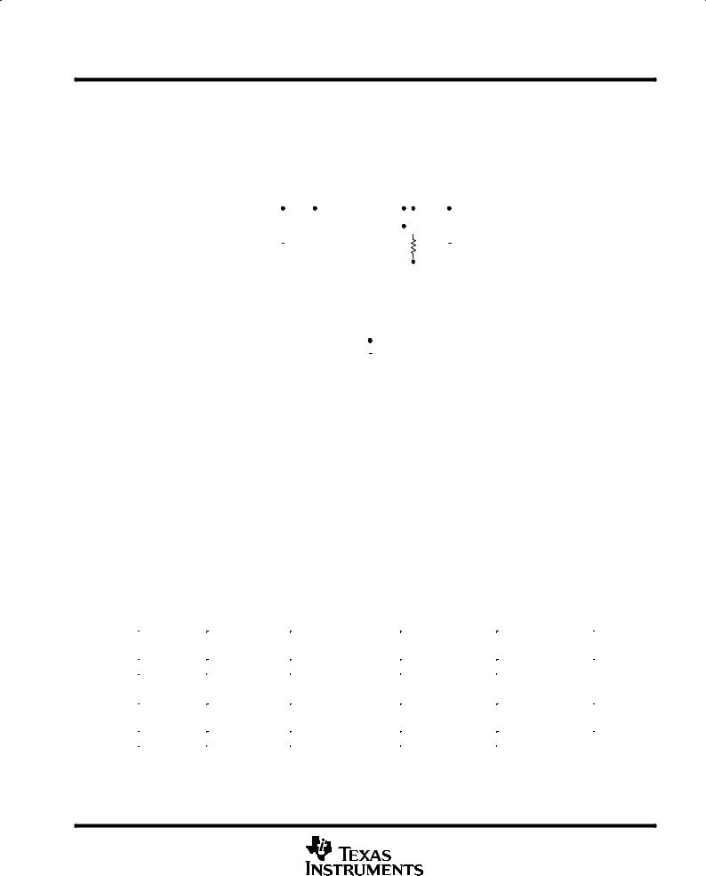
VOUT
|
|
IN |
VBAT |
|
R3 |
|
|
|
|
|
|
|
|
|
R1 |
|
|
|
R1 |
LBO |
_ |
LBI |
VTRIP + 1.21 V 1 ) R2 |
|
+ |
|
R2 |
|
VREF |
+ |
|
|
± |
|
Figure 1. Programming of the Low-Battery Comparator Trip Voltage
Formulas to calculate the resistive divider for low battery detection, with VLBI = 1.15 V ± 1.27 V:
R2 + 1 MW VLBI
VBAT
R1 + 1 MW * R2
Formulas to calculate the minimum and maximum battery voltage that triggers the low battery detector:
VBAT(min) + VLBI(min) |
R1(min) ) R2(max) |
|
|
|
R2(max) |
||
|
|
||
VBAT(max) + VLBI(max) |
|
R1(max) ) R2(min) |
|
|
R2(min) |
||
|
|
||
Table 1. Recommended Values for the Resistive Divider from the E96 Series (±1%),
VLBI = 1.15 V ± 1.27 V
VBAT/V |
R1/kΩ |
R2/kΩ |
VBAT(MIN)/V |
VBAT(MAX)/V |
||
2.7 |
562 |
453 |
2.548 |
±5.61% |
2.877 |
6.57% |
|
|
|
|
|
|
|
2.8 |
576 |
442 |
2.619 |
±6.47% |
2.958 |
5.66% |
|
|
|
|
|
|
|
2.9 |
590 |
422 |
2.726 |
±6.00% |
3.081 |
6.26% |
|
|
|
|
|
|
|
3.0 |
590 |
402 |
2.804 |
±6.53% |
3.172 |
5.72% |
|
|
|
|
|
|
|
3.1 |
604 |
383 |
2.928 |
±5.56% |
3.313 |
6.88% |
|
|
|
|
|
|
|
3.2 |
619 |
374 |
3.016 |
±5.76% |
3.414 |
6.70% |
|
|
|
|
|
|
|
3.3 |
649 |
374 |
3.106 |
±5.88% |
3.518 |
6.62% |
|
|
|
|
|
|
|
A 100 nF bypass capacitor should be connected in parallel to R2 if large line transients are expected. These voltage drops can inadvertently trigger the low-battery comparator and produce a wrong low-battery warning signal at the LBO pin.
6 |
POST OFFICE BOX 655303 •DALLAS, TEXAS 75265 |
TPS60130, TPS60131, TPS60132, TPS60133
REGULATED 5-V, 300 mA HIGH EFFICIENCY CHARGE PUMP
DC/DC CONVERTERS
SLVS258A ± NOVEMBER 1999 ± REVISED DECEMBER 1999
Power-Good detector (TPS60131 and TPS60133)
The PG pin is an open-drain output that is pulled low when the output is out of regulation. When the output voltage rises to about 90% of its nominal voltage, power-good output is released. PG is high impedance when the device is disabled. An external pullup resistor must be connected between PG and OUT. The pullup resistor should be in the 100 kΩ to 1 MΩ range. If the power-good function is not used, the PG-pin should remain unconnected.
TPS60131
Input |
|
|
IN |
OUT |
|
|
|
|
|
|
|
|
|
|
|
|
|
|
|
|
Output |
||||||||||||||||||
2.7 V to 5.4 V |
|
|
|
|
|
|
|
|
|
|
|
|
|
|
|
|
|
|
|
|
|
|
|
|
|
|
|
5 V, 300 mA |
|||||||||||
|
|
|
|
|
|
|
|
|
|
|
|
|
|
|
|
|
|
|
|
|
|
|
|
|
|
|
|
|
|
|
|||||||||
|
Ci |
|
|
|
|
|
|
|
|
|
|
IN |
OUT |
|
|
|
|
|
|
|
|
|
|
|
|
|
|
|
Co |
||||||||||
|
|
|
|
|
|
|
|
|
|
|
|
|
|
|
|
|
|
|
|
|
|
|
|
|
|
||||||||||||||
|
15 µF |
|
|
|
|
|
|
|
|
|
|
|
|
|
|
|
|
|
|
|
|
|
|
|
|
|
|||||||||||||
|
|
|
|
|
|
|
|
|
|
|
|
|
|
|
|
|
|
|
|
|
|
|
|
|
|
|
|
|
|
|
|
|
|
|
|
|
|
33 µF |
|
|
|
|
|
|
|
|
|
|
|
|
|
|
|
|
|
NC |
|
|
FB |
|
|
|
|
|
|
|
|
R1 |
|
|
|
||||||||
|
|
|
|
|
|
|
|
|
|
|
|
|
|
|
|
|
|
|
|
|
|
|
|
|
|
|
|
|
|
|
|||||||||
|
|
|
|
|
|
|
|
|
|
|
|
|
|
|
|
|
|
|
|
PG |
|
|
|
|
|
|
|
|
1 MΩ |
|
|
|
|
Power-Good Output |
|||||
|
|
|
|
|
|
|
|
|
|
|
|
|
|
|
|
|
|
|
|
|
|
|
|
|
|
|
|
|
|
|
|
||||||||
|
|
|
|
|
|
|
|
|
|
|
|
|
|
|
|
|
|
|
|
|
|
|
|
|
|
|
|
|
|
|
|
|
|
|
|
||||
|
|
|
|
|
|
|
|
|
|
|
|
|
|
|
|
|
|
|
|
|
|
|
|
|
|
|
|
|
|
|
|
|
|
|
|
||||
|
|
|
|
|
|
|
C1 |
|
|
|
|
|
C1+ |
|
C2+ |
|
|
|
|
|
|
|
C2 |
|
|
|
|
|
|||||||||||
|
|
|
|
|
|
|
|
|
|
|
|
|
|
|
|
|
|
|
|
|
|
|
|
||||||||||||||||
|
|
|
|
|
|
|
|
|
|
|
|
C1± |
|
|
|
|
|
|
|
|
|
|
|
|
|
|
|
|
|
||||||||||
|
|
2.2 µF |
|
|
|
|
C2± |
|
|
|
|
|
|
|
2.2 µF |
|
|
|
|
|
|||||||||||||||||||
|
|
|
|
|
|
|
|
|
|
|
|||||||||||||||||||||||||||||
|
|
|
|
|
|
|
|
|
|
|
|
|
|
|
|
ENABLE |
|
|
|
|
|
|
|
|
|
|
|
|
|
|
|
|
|
|
|
|
|
|
|
|
|
|
|
|
|
Off/On |
|
PGND GND |
|
|
|
|
|
|
|
|
|
|
|
|
|
|
|
|
|
||||||||||||||
|
|
|
|
|
|
|
|
|
|
|
|
|
|
|
|
|
|
|
|
|
|
|
|
|
|
|
|
|
|
|
|
|
|
|
|
|
|
|
|
|
|
|
|
|
|
|
|
|
|
|
|
|
|
|
|
|
|
|
|
|
|
|
|
|
|
|
|
|
|
|
|
|
|
|
|
|
|
|
|
Figure 2. Typical Operating Circuit Using Power-Good Comparator
absolute maximum ratings (see Note 1)²
Input voltage range, VI (IN, OUT, ENABLE, FB, LBI, LBO/PG) . . . . . . . . . . . . . . . . . . . . . . . . . . . ±0.3 V to 5.5 V
Differential input voltage, VID (C1+, C2+ to GND) . . . . . . . . . . . . . . . . . . . . . . . . . . . . . . ±0.3 V to (VO + 0.3 V) Differential input voltage, VID (C1±, C2± to GND) . . . . . . . . . . . . . . . . . . . . . . . . . . . . . . . . ±0.3 V to (VI + 0.3 V) Continuous total power dissipation . . . . . . . . . . . . . . . . . . . . . . . . . . . . . . . . . . . . . . See Dissipation Rating Table
Continuous output current: TPS60130, TPS60131 . . . . . . . . . . . . . . . . . . . . . . . . . . . . . . . . . . . . . . . . . . 400 mA TPS60132, TPS60133 . . . . . . . . . . . . . . . . . . . . . . . . . . . . . . . . . . . . . . . . . . 200 mA
Storage temperature range, Tstg . . . . . . . . . . . . . . . . . . . . . . . . . . . . . . . . . . . . . . . . . . . . . . . . . . . . ±55°C to 150°C Lead temperature 1,6 mm (1/16 inch) from case for 10s . . . . . . . . . . . . . . . . . . . . . . . . . . . . . . . . . . . . . . . 260°C
Maximum junction temperature, TJ . . . . . . . . . . . . . . . . . . . . . . . . . . . . . . . . . . . . . . . . . . . . . . . . . . . . . . . . . 150°C
²Stresses beyond those listed under ªabsolute maximum ratingsº may cause permanent damage to the device. These are stress ratings only, and functional operation of the device at these or any other conditions beyond those indicated under ªrecommended operating conditionsº is not implied. Exposure to absolute-maximum-rated conditions for extended periods may affect device reliability.
NOTE 1: V(ENABLE),V(LBI)andV(LBO/PG)canexceedVIuptothemaximumratedvoltagewithoutincreasingtheleakagecurrentdrawnbythese
inputs.
DISSIPATION RATING TABLE FREE-AIR TEMPERATURE (see Figure 1)
PACKAGE |
TA ≤ 25°C |
DERATING FACTOR |
TA = 70°C |
TA = 85°C |
|
POWER RATING |
ABOVE TA = 25°C |
POWER RATING |
POWER RATING |
||
|
|||||
PWP |
700 mW |
5.6 mW/°C |
448 mW |
364 mW |
|
|
DISSIPATION RATING TABLE CASE TEMPERATURE (see Figure 2) |
||||
|
|
|
|
|
|
PACKAGE |
TC ≤ 62.5°C |
DERATING FACTOR |
TC = 70°C |
TC = 85°C |
|
POWER RATING |
ABOVE TC = 62.5°C |
POWER RATING |
POWER RATING |
||
|
|||||
PWP |
25 mW |
285.7 mW/°C |
22.9 mW |
18.5 mW |
|
POST OFFICE BOX 655303 •DALLAS, TEXAS 75265 |
7 |
 Loading...