


Texas Instruments TPS70758PWPR, TPS70758PWP, TPS70751PWPR, TPS70751PWP, TPS70748PWPR Datasheet
...TPS70745, TPS70748, TPS70751, TPS70758, TPS70702 DUAL-OUTPUT LOW-DROPOUT VOLTAGE REGULATORS WITH POWER UP SEQUENCING FOR SPLIT VOLTAGE DSP SYSTEMS
SLVS291 ± MAY 2000
DDual Output Voltages for Split-Supply Applications
DSelectable Power Up Sequencing for DSP Applications
DOutput Current Range of 250 mA on Regulator 1 and 125 mA on Regulator 2
DFast Transient Response
DVoltage Options are 3.3-V/2.5-V, 3.3-V/1.8-V, 3.3-V/1.5-V, 3.3-V/1.2-V, and Dual Adjustable Outputs
DOpen Drain Power-On Reset With 120-ms Delay
description
DOpen Drain Power Good for Regulator 1
DUltra Low 190 A (typ) Quiescent Current
D1 A Input Current During Standby
DLow Noise: 65 VRMS Without Bypass
Capacitor
DQuick Output Capacitor Discharge Feature
DTwo Manual Reset Inputs
D2% Accuracy Over Load and Temperature
DUndervoltage Lockout (UVLO) Feature
D20-Pin PowerPAD TSSOP Package
DThermal Shutdown Protection
PWP PACKAGE
(TOP VIEW)
TPS707xx family devices are designed to provide a complete power management solution for DSP, processor power, ASIC, FPGA, and digital applications where dual output voltage regulators are required. Easy programmability of the sequencing function makes this family ideal for any DSP applications with power sequencing requirement. Differentiated features, such as accuracy, fast transient response, SVS supervisory circuit (power on reset), manual reset inputs, and enable function, provide a complete system solution.
|
NC |
|
1 |
20 |
|
|
|
NC |
||||
|
|
|
|
|||||||||
|
VIN1 |
|
|
2 |
19 |
|
|
|
VOUT1 |
|||
|
|
|
|
|||||||||
|
|
|
|
|||||||||
|
VIN1 |
|
|
3 |
18 |
|
|
|
VOUT1 |
|||
|
|
|
|
|||||||||
|
|
|
|
|
||||||||
|
MR1 |
|
|
|
4 |
17 |
|
|
|
VSENSE1/FB1 |
||
|
|
|
|
|||||||||
|
|
|
||||||||||
|
MR2 |
|
|
|
5 |
16 |
|
|
|
PG1 |
||
|
|
|
|
|||||||||
|
|
EN |
|
|
|
6 |
15 |
|
|
|
RESET |
|
|
|
|||||||||||
|
|
|
|
|||||||||
SEQ |
|
|
7 |
14 |
|
|
|
VSENSE2/FB2 |
||||
|
|
|
|
|||||||||
|
|
|
|
|||||||||
GND |
|
|
8 |
13 |
|
|
|
VOUT2 |
||||
|
|
|
|
|||||||||
|
VIN2 |
|
|
9 |
12 |
|
|
|
VOUT2 |
|||
|
|
|
|
|||||||||
|
VIN2 |
|
|
10 |
11 |
|
|
|
NC |
|||
|
|
|
|
|
|
|
|
|||||
|
|
TPS70751 PWP |
|
|
|
DSP |
I/O |
|
|
|
|
VOUT1 |
|
|
3.3 V |
||
5 V |
VIN1 |
|
|
|
|
|||
|
|
|
|
|
||||
|
|
0.1 µF |
VSENSE1 |
|
10 µF |
|
|
|
|
|
|
|
|
250 kΩ |
|
|
|
|
|
|
|
|
|
|
|
|
|
|
|
PG1 |
|
|
PG1 |
|
|
|
|
|
|
|
|
|
|
|
|
|
VIN2 |
MR2 |
MR2 |
>2 V |
|
|
|
|
|
|
|
|
|
|||
|
|
|
|
<0.7 V |
250 kΩ |
|
|
|
|
|
|
|
|
|
|
||
|
|
0.1 µF |
RESET |
|
|
|
RESET |
|
|
|
|
|
|
|
|
||
>2 V |
EN |
EN |
MR1 |
MR1 |
>2 V |
|
|
|
|
|
|
|
<0.7 V |
|
|
||
|
<0.7 V |
|
|
|
|
|
||
|
|
|
VSENSE2 |
|
|
|
|
|
|
|
SEQ |
|
|
|
1.8 V |
|
|
|
|
|
VOUT2 |
|
|
Core |
|
|
|
|
|
|
10 µF |
|
|
||
|
|
|
|
|
|
|
|
|
Please be aware that an important notice concerning availability, standard warranty, and use in critical applications of Texas Instruments semiconductor products and disclaimers thereto appears at the end of this data sheet.
PowerPAD is a trademark of Texas Instruments Incorporated.
PRODUCTION DATA information is current as of publication date. Products conform to specifications per the terms of Texas Instruments standard warranty. Production processing does not necessarily include testing of all parameters.
Copyright 2000, Texas Instruments Incorporated
POST OFFICE BOX 655303 •DALLAS, TEXAS 75265 |
1 |

TPS70745, TPS70748, TPS70751, TPS70758, TPS70702 DUAL-OUTPUT LOW-DROPOUT VOLTAGE REGULATORS
WITH POWER UP SEQUENCING FOR SPLIT VOLTAGE DSP SYSTEMS
SLVS291 ± MAY 2000
description (continued)
The TPS707xx family of voltage regulators offers very low dropout voltage and dual outputs with power up sequence control, which is designed primarily for DSP applications. These devices have extremely low noise output performance without using any added filter bypass capacitors and are designed to have a fast transient response and be stable with 10 uF low ESR capacitors.
These devices have fixed 3.3-V/2.5-V, 3.3-V/1.8-V, 3.3-V/1.5-V, 3.3-V/1.2-V, and adjustable/adjustable voltage options. Regulator 1 can support up to 250 mA and regulator 2 can support up to 125 mA. Separate voltage inputs allow the designer to configure the source power.
Because the PMOS device behaves as a low-value resistor, the dropout voltage is very low (typically 83 mV on regulator 1) and is directly proportional to the output current. Additionally, since the PMOS pass element is a voltage-driven device, the quiescent current is very low and independent of output loading (maximum of 230 A over the full range of output current). This LDO family also features a sleep mode; applying a high signal to EN (enable) shuts down both regulators, reducing the input current to 1 A at TJ = 25°C.
The device is enabled when the EN pin is connected to a low-level input voltage. The output voltages of the two regulators are sensed at the VSENSE1 and VSENSE2 pins respectively.
The input signal at the SEQ pin controls the power-up sequence of the two regulators. When the device is
enabled and the SEQ terminal is pulled high or left open, VOUT2 will turn on first and VOUT1 will remain off until VOUT2 reaches approximately 83% of its regulated output voltage. At that time VOUT1 will be turned on. If VOUT2 is pulled below 83% (i.e. over load condition) VOUT1 will be turned off. Pulling the SEQ terminal low, reverses the power-up order and VOUT1 will be turned on first. The SEQ pin is connected to an internal pullup current source.
For each regulator, there is an internal discharge transistor to discharge the output capacitor when the regulator is turned off(disabled).
The PG1 pin reports the voltage conditions at VOUT1. Power good can be used to implement a SVS for the circuitry supplied by regulator 1.
The TPS707xx features a RESET (SVS, POR, or Power On Reset). RESET output initiates a reset in DSP systems and related digital applications in the event of an undervoltage condition. RESET indicates the status of VOUT2 and both manual reset pins (MR1 and MR2). When VOUT2 reaches 95% of its regulated voltage and
MR1 and MR2 are in the logic high state, RESET will go to a high impedance state after 120 ms delay. RESET will go to logic low state when VOUT2 regulated output voltage is pulled below 95% (i.e. over load condition) of
its regulated voltage. To monitor VOUT1 , the PG1 output pin can be connected to MR1 or MR2.
The device has an undervoltage lockout UVLO circuit which prevents the internal regulators from turning on until VIN1 reaches 2.5V.
AVAILABLE OPTIONS
TJ |
REGULATOR 1 |
REGULATOR 2 |
TSSOP |
|
VO (V) |
VO (V) |
(PWP) |
||
|
||||
|
3.3 V |
1.2 V |
TPS70745PWP |
|
|
|
|
|
|
|
3.3 V |
1.5 V |
TPS70748PWP |
|
|
|
|
|
|
±40°C to 125°C |
3.3 V |
1.8 V |
TPS70751PWP |
|
|
|
|
||
3.3 V |
2.5 V |
TPS70758PWP |
||
|
||||
|
|
|
|
|
|
Adjustable |
Adjustable |
TPS70702PWP |
|
|
(1.22 V to 5.5 V) |
(1.22 V to 5.5 V) |
||
|
|
|||
|
|
|
|
NOTE: The TPS70702 is programmable using external resistor dividers (see application information) The PWP package is available taped and reeled. Add an R suffix to the device type (e.g., TPS70702PWPR).
2 |
POST OFFICE BOX 655303 •DALLAS, TEXAS 75265 |
TPS70745, TPS70748, TPS70751, TPS70758, TPS70702 DUAL-OUTPUT LOW-DROPOUT VOLTAGE REGULATORS WITH POWER UP SEQUENCING FOR SPLIT VOLTAGE DSP SYSTEMS
SLVS291 ± MAY 2000
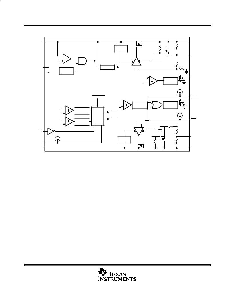
detailed block diagram ± fixed voltage version
VIN1 (2 Pins) |
VOUT1 (2 Pins) |
Current |
10 kΩ |
Sense |
|
ENA_1 |
VSENSE1 |
UVLO |
(see Note A) |
Shutdown
2.5 V |
ENA_1 |
|
Reference |
± |
+ |
|
GND |
VREF |
|
FB1 |
|
|
Thermal |
VREF |
|
|
|
Shutdown |
|
|
|
|
|
|
|
|
|
|
|
FB1 |
PG1 |
|
|
|
Rising Edge |
|
|
|
|
|
|
|
|
0.95 × VREF |
Deglitch |
|
|
|
|
||
|
|
|
|
VIN1 |
|
|
SHUTDOWN |
|
|
|
MR2 |
|
|
|
FB2 |
|
|
RESET |
|
UV Comp |
|
Rising Edge |
Falling Edge |
||
|
|
|
||||
FB2 |
|
|
0.95 × VREF |
Deglitch |
|
Delay |
Falling Edge |
|
|
|
VIN1 |
||
|
|
|
|
|
||
0.83 × VREF |
Deglitch |
Power |
ENA_1 |
|
|
|
|
|
|
||||
|
|
|
|
|
||
|
|
Sequence |
|
|
|
|
FB1 |
Falling Edge |
Logic |
ENA_2 |
VREF |
|
MR1 |
|
|
|
FB2 |
|||
0.83 × VREF |
Deglitch |
|
|
|
|
|
|
|
|
|
|
||
|
|
|
|
|
|
|
|
UV Comp |
|
|
± + |
|
|
EN |
VIN1 |
ENA_2 |
|
|
|
VSENSE2 |
|
|
|
ENA_2 |
|
|
Current |
(see Note A) |
|
|
|
||
SEQ |
Sense |
|
10 kΩ |
(see Note B) |
|
|
|
|
|
|
|
VIN2 (2 Pins) |
|
|
VOUT2(2 Pins) |
NOTES: A. For most applications, VSENSE1 and VSENSE2 should be externally connected to VOUT as close as possible to the device. For other implementations, refer to SENSE terminal connection discussion in the application information section.
B. If the SEQ terminal is floating at the input, VOUT2 will power up first.
POST OFFICE BOX 655303 •DALLAS, TEXAS 75265 |
3 |

TPS70745, TPS70748, TPS70751, TPS70758, TPS70702 DUAL-OUTPUT LOW-DROPOUT VOLTAGE REGULATORS
WITH POWER UP SEQUENCING FOR SPLIT VOLTAGE DSP SYSTEMS
SLVS291 ± MAY 2000
detailed block diagram ± adjustable voltage version
VIN1 (2 Pins) |
VOUT1 (2 Pins) |
Current |
Sense |
ENA_1
|
UVLO |
FB1 |
|
Shutdown |
|
2.5 V |
ENA_1 |
(see Note A) |
|
Reference |
± |
+ |
|
GND |
VREF |
|
|
|
Thermal |
VREF |
|
||
|
|
|||
|
Shutdown |
|
||
|
|
|
PG1 |
|
|
|
|
FB1 |
|
|
|
|
Rising Edge |
|
|
|
|
|
|
|
|
0.95 × VREF |
Deglitch |
|
|
|
|
||
|
|
|
|
VIN1 |
SHUTDOWN |
MR2 |
|
|
|
FB2 |
|
|
RESET |
|
UV Comp |
|
Rising Edge |
Falling Edge |
||
|
|
|
||||
FB2 |
|
|
0.95 × VREF |
Deglitch |
Delay |
|
Falling Edge |
|
VIN1 |
||||
|
|
|
|
|
||
0.83 × VREF |
Deglitch |
Power |
ENA_1 |
|
|
|
|
|
|
||||
|
Sequence |
|
|
|
|
|
|
|
|
|
|
|
|
FB1 |
Falling Edge |
Logic |
ENA_2 |
|
|
|
|
|
|
MR1 |
|||
|
|
|
VREF |
|
||
|
Deglitch |
|
|
|
||
0.83 × VREF |
|
|
|
|
||
|
|
|
|
|
|
|
|
UV Comp |
|
|
± |
+ |
|
EN |
|
|
|
|
||
VIN1 |
|
|
|
|
ENA_2 |
|
|
|
|
|
|
ENA_2 |
FB2 |
|
|
|
|
Current |
(see Note A) |
|
SEQ |
|
|
|
|
||
|
|
|
Sense |
|
|
|
(see Note B) |
|
|
|
|
|
|
VIN2 (2 Pins) |
|
|
|
|
|
VOUT2 (2 Pins) |
|
|
|
|
|
|
|
NOTES: A. For most applications, FB1 and FB2 should be externally connected to resistor dividers as close as possible to the device. For other implementations, refer to FB terminals connection discussion in the application information section.
B. If the SEQ terminal is floating at the input, VOUT2 will power up first.
4 |
POST OFFICE BOX 655303 •DALLAS, TEXAS 75265 |

TPS70745, TPS70748, TPS70751, TPS70758, TPS70702 DUAL-OUTPUT LOW-DROPOUT VOLTAGE REGULATORS WITH POWER UP SEQUENCING FOR SPLIT VOLTAGE DSP SYSTEMS
SLVS291 ± MAY 2000
RESET timing diagram (with VIN1 powered up and MR1 AND MR2 at logic high)
VRES
(see Note A)
VIN2
 VRES t
VOUT2 |
|
|
|
V (see Note B) |
|
|
|
|
|
|
|
V |
(see Note B) |
|
|
|
|
|
IT + |
|
|
|
|
|
|
|
|
IT + |
|
Threshold |
|
|
|
|
|
|
|
|
|
|
|
|
|
|
Voltage |
|
|
|
VIT ± |
|
|
|
|
|
|
|
|
|
|
|
|
|
|
|
|
|
|
|
|
|
|
|
|
|
|
|
|
|
|
|
|
|
|
VIT ± |
|||||
|
|
|
|
(see Note B) |
|
|
|
|
|
|
|
|
(see Note B) |
|
|
|
t |
RESET |
120 ms |
120 ms |
Output |
||
|
Delay |
Delay |
Output |
|
Output |
Undefined |
|
Undefined |
|
|
t |
NOTES: A. VRES is the minimum input voltage for a valid RESET. The symbol Vres is not currently listed within EIA or JEDEC standards for semiconductor symbology
B. VIT ±Trip voltage is typically 5% lower than the output voltage (95%VO) VIT± to VIT+ is the hysteresis voltage.
PG1 timing diagram
VUVLO
VPG1
(see Note A)
VIN1 |
VUVLO |
VPG1 |
t |
VOUT2 |
V (see Note B) |
V (see Note B) |
|
IT + |
IT+ |
Threshold
Voltage
VIT ± |
VIT ± |
(see Note B) |
(see Note B) |
|
30 s |
|
t |
PG1 |
|
Output |
|
Output |
Output |
Undefined |
Undefined |
|
t |
NOTES: A. VPG1 is the minimum input voltage for a valid PG1. The symbol VPG1 is not currently listed within EIA or JEDEC standards for semiconductor symbology.
B. VIT ±Trip voltage is typically 5% lower than the output voltage (95%VO) VIT± to VIT+ is the hysteresis voltage.
POST OFFICE BOX 655303 •DALLAS, TEXAS 75265 |
5 |

TPS70745, TPS70748, TPS70751, TPS70758, TPS70702 DUAL-OUTPUT LOW-DROPOUT VOLTAGE REGULATORS
WITH POWER UP SEQUENCING FOR SPLIT VOLTAGE DSP SYSTEMS
SLVS291 ± MAY 2000
|
|
|
|
|
|
|
Terminal Functions |
|
|
|
|
|
|
|
|
|
|
|
|
TERMINAL |
I/O |
DESCRIPTION |
|
|
|
NAME |
NO. |
||||
|
|
|
|
||||
|
|
|
|
|
|
|
|
|
|
|
|
|
6 |
I |
Active low enable |
|
EN |
|
|
|
|||
|
|
|
|
|
|
|
|
|
GND |
8 |
|
Ground |
|||
|
|
|
|
|
|
||
|
|
|
|
|
4 |
I |
Manual reset input 1, active low, pulled up internally |
|
MR1 |
|
|
||||
|
|
|
|
|
|
||
|
|
|
|
|
5 |
I |
Manual reset input 2, active low, pulled up internally |
|
MR2 |
|
|
||||
|
NC |
1, 11, 20 |
|
No connection |
|||
|
|
|
|
|
|
||
|
PG1 |
16 |
O |
Open drain output, low when VOUT1 voltage is less than 95% of the nominal regulated voltage |
|||
|
|
|
|
|
15 |
O |
Open drain output, SVS (power on reset) signal, active low |
|
RESET |
|
|||||
|
|
|
|
|
|||
|
SEQ |
7 |
I |
Power up sequence control: SEQ=High, VOUT2 powers up first; SEQ=Low, VOUT1 powers up first, SEQ |
|||
|
|
|
|
|
|
|
terminal pulled up internally. |
|
|
|
|
|
|||
|
VIN1 |
2, 3 |
I |
Input voltage of regulator 1 |
|||
|
VIN2 |
9, 10 |
I |
Input voltage of regulator 2 |
|||
|
VOUT1 |
18, 19 |
O |
Output voltage of regulator 1 |
|||
|
VOUT2 |
12, 13 |
O |
Output voltage of regulator 2 |
|||
|
VSENSE2/FB2 |
14 |
I |
Regulator 2 output voltage sense/ regulator 2 feedback for adjustable |
|||
|
VSENSE1/FB1 |
17 |
I |
Regulator 1 output voltage sense/ regulator 1 feedback for adjustable |
|||
absolute maximum ratings over operating junction temperature (unless otherwise noted)²
Input voltage range³ : V . . . . . . . . . . . . . . . . . . . . . . . . . . . . . . . . . . . . . . . . . . . . |
. . . . . . . . . . . . . . ±0.3 V to 7 V |
|||||||||
|
|
|
|
|
|
|
|
IN1 |
|
|
|
|
|
|
|
|
|
|
VIN2 . . . . . . . . . . . . . . . . . . . . . . . . . . . . . . . . . . . . . . . . . . . . |
. . . . . . . . . . . . . . ±0.3 V to 7 |
V |
Voltage range at |
EN |
|
. . . . . . . . . . . . . . . . . . . . . . . . . . . . . . . . . . . . . . . . . . . . . . . . . . |
. . . . . . . . . . . . . . ±0.3 V to 7 |
V |
|||||
Output voltage range (VOUT1, VSENSE1) . . . . . . . . . . . . . . . . . . . . . . . . . . . . . . . |
. . . . . . . . . . . . . . . . . . . . . 5.5 |
V |
||||||||
Output voltage range (VOUT2, VSENSE2) . . . . . . . . . . . . . . . . . . . . . . . . . . . . . . . |
. . . . . . . . . . . . . . . . . . . . . 5.5 |
V |
||||||||
Maximum |
RESET, |
. . . . . . . . . . . . . . . . . . . . . . . . . . . . . . . . . . . . . . . .PG1 voltage |
. . . . . . . . . . . . . . . . . . . . . . . 7 V |
|||||||
Maximum |
MR1, |
|
MR2, |
. . . . . . . . . . . . . . . . . . . . . . . . . . . . . . . . .and SEQ voltage |
. . . . . . . . . . . . . . . . . . . . . . VIN1 |
|||||
Peak output current . . . . . . . . . . . . . . . . . . . . . . . . . . . . . . . . . . . . . . . . . . . . . . . . . . |
. . . . . . . . . . . . Internally limited |
|||||||||
Continuous total power dissipation . . . . . . . . . . . . . . . . . . . . . . . . . . . . . . . . . . . . |
See Dissipation Rating Tables |
|||||||||
Operating virtual junction temperature range, TJ . . . . . . . . . . . . . . . . . . . . . . . . . |
. . . . . . . . . . . . ±40°C to 125°C |
|||||||||
Storage temperature range, Tstg . . . . . . . . . . . . . . . . . . . . . . . . . . . . . . . . . . . . . . . |
. . . . . . . . . . . . ±65°C to 150°C |
|||||||||
ESD rating, HBM . . . . . . . . . . . . . . . . . . . . . . . . . . . . . . . . . . . . . . . . . . . . . . . . . . . . |
. . . . . . . . . . . . . . . . . . . . . . 2 kV |
|||||||||
² Stresses beyond those listed under ªabsolute maximum ratingsº may cause permanent damage to the device. These are stress ratings only, and functional operation of the device at these or any other conditions beyond those indicated under ªrecommended operating conditionsº is not implied. Exposure to absolute-maximum-rated conditions for extended periods may affect device reliability.
³ All voltages are tied to network ground.
DISSIPATION RATING TABLE
PACKAGE |
AIR FLOW |
|
TA ≤ 25°C |
DERATING FACTOR |
|
TA = 70°C |
TA = 85°C |
(CFM) |
|
|
|||||
|
|
|
|
|
|
|
|
|
|
|
|
|
|
|
|
PWP§ |
0 |
|
3.067 W |
30.67 mW/°C |
|
1.687 W |
1.227 W |
250 |
|
4.115 W |
41.15 mW/°C |
|
2.265 W |
1.646 W |
|
|
|
|
§This parameter is measured with the recommended copper heat sink pattern on a 4-layer PCB, 1 oz. copper on 4-in ×4-in ground layer. For more information, refer to TI technical brief SLMA002.
6 |
POST OFFICE BOX 655303 •DALLAS, TEXAS 75265 |

TPS70745, TPS70748, TPS70751, TPS70758, TPS70702 DUAL-OUTPUT LOW-DROPOUT VOLTAGE REGULATORS WITH POWER UP SEQUENCING FOR SPLIT VOLTAGE DSP SYSTEMS
SLVS291 ± MAY 2000
recommended operating conditions
|
MIN |
MAX |
UNIT |
|
|
|
|
Input voltage, VI² |
2.7 |
6 |
V |
Output current, IO (regulator 1) |
0 |
250 |
mA |
Output current, IO (regulator 2) |
0 |
125 |
mA |
Output voltage range (for adjustable option) |
1.22 |
5.5 |
V |
|
|
|
|
Operating virtual junction temperature, TJ |
±40 |
125 |
°C |
² To calculate the minimum input voltage for maximum output current, use the following equation: VI(min) = VO(max) + VDO(max load).
electrical characteristics over recommended operating junction temperature (TJ = ±40°C to 125°C) VIN1 or VIN2 = VO(nom) + 1 V, IO = 1 mA, EN = 0, CO = 33 F(unless otherwise noted)
|
PARAMETER |
|
|
|
|
|
TEST CONDITIONS |
|
MIN |
TYP |
MAX |
UNIT |
|
|
|
|
|
|
|
|
|
|
|
|
|
|
|
|
|
|
|
Reference |
2.7 |
V < VI < 6 V, |
FB connected to VO |
|
1.22 |
|
|
||
|
|
|
|
|
TJ = 25°C |
|
|
|
|
|
|||
|
|
|
|
voltage |
|
|
|
|
|
|
|
||
|
|
|
|
2.7 |
V < VI < 6 V, |
FB connected to VO |
1.196 |
|
1.244 |
|
|||
|
|
|
|
|
|
|
|||||||
|
|
|
|
1.2 V Output |
2.7 |
V < VI < 6 V, |
TJ = 25°C |
|
|
1.2 |
|
|
|
|
|
|
|
2.7 |
V < VI < 6 V |
|
|
1.176 |
|
1.224 |
|
||
|
|
|
|
|
|
|
|
|
|||||
|
Output voltage |
|
|
1.5 V Output |
2.7 |
V < VI < 6 V, |
TJ = 25°C |
|
|
1.5 |
|
V |
|
V |
|
|
2.7 |
V < VI < 6 V |
|
|
1.47 |
|
1.53 |
|
|||
|
|
|
|
|
|
|
|||||||
|
|
|
|
|
|
|
|
||||||
O |
(see Notes 1 and 3) |
|
|
1.8 V Output |
2.8 |
V < VI < 6 V, |
TJ = 25°C |
|
|
1.8 |
|
|
|
|
|
|
|
|
|
|
|
||||||
|
|
|
|
2.8 |
V < VI < 6 V |
|
|
1.764 |
|
1.836 |
|
||
|
|
|
|
|
|
|
|
|
|||||
|
|
|
|
2.5 V Output |
3.5 |
V < VI < 6 V, |
TJ = 25°C |
|
|
2.5 |
|
|
|
|
|
|
|
3.5 |
V < VI < 6 V |
|
|
2.45 |
|
2.55 |
|
||
|
|
|
|
|
|
|
|
|
|||||
|
|
|
|
3.3 V Output |
4.3 |
V < VI < 6 V, |
TJ = 25°C |
|
|
3.3 |
|
V |
|
|
|
|
|
4.3 |
V < VI < 6 V |
|
|
3.234 |
|
3.366 |
|||
|
|
|
|
|
|
|
|
|
|||||
Quiescent current (GND current) for regulator 1 and |
|
See Note 3, |
TJ = 25°C |
|
|
190 |
|
A |
|||||
regulator 2, EN = 0 V, (see Note 1) |
|
|
|
|
See Note 3 |
|
|
|
|
230 |
|||
|
|
|
|
|
|
|
|
|
|||||
|
|
|
|
|
|
|
|
|
|
|
|
|
|
Output voltage line regulation ( V /V |
|
) for |
|
VO + 1 V < VI ≤ 6 V, |
TJ = 25°C, |
See Note 1 |
|
0.01% |
|
|
|||
|
O |
O |
|
|
|
|
|
|
|
|
|
|
V |
regulator 1 and regulator 2 (see Note 2) |
|
VO + 1 V < VI ≤ 6 V, |
See Note 1 |
|
|
|
0.1% |
||||||
|
|
|
|
|
|||||||||
Load regulation for VOUT1 and VOUT2 |
|
TJ = 25°C, |
See Note 3 |
|
|
1 |
|
mV |
|||||
Vn |
Output noise voltage |
|
|
Regulator 1 |
|
BW = 300 Hz to 50 kHz, |
CO = 33 F, |
TJ = 25°C |
|
65 |
|
Vrms |
|
|
|
|
|
|
|
|
|||||||
|
|
Regulator 2 |
|
65 |
|
||||||||
|
|
|
|
|
|
|
|
|
|
|
|
||
|
|
|
|
|
|
|
|
|
|
|
|
|
|
Output current limit |
|
|
Regulator 1 |
|
VO = 0 V |
|
|
|
1.6 |
1.9 |
A |
||
|
|
|
|
|
|
|
|
|
|||||
|
|
Regulator 2 |
|
|
|
0.750 |
1 |
||||||
|
|
|
|
|
|
|
|
|
|
|
|||
|
|
|
|
|
|
|
|
|
|
|
|||
Thermal shutdown junction temperature |
|
|
|
|
|
|
150 |
|
°C |
||||
|
|
|
|
|
|
|
|
|
|
|
|
|
|
II(standby) Standby current |
|
|
Regulator 1 and |
|
EN |
= VI, |
TJ = 25°C |
|
|
|
2 |
A |
|
|
|
Regulator 2 |
|
|
|
|
|
|
|
|
|||
|
|
|
EN = VI |
|
|
|
|
6 |
|||||
|
|
|
|
|
|
|
|
|
|
||||
|
|
|
|
|
|
|
|
|
|
|
|||
PSRR |
Power supply ripple rejection |
|
f = 1 kHz, CO = 33 µF, |
TJ = 25°C, |
See Note 1 |
|
60 |
|
dB |
||||
NOTES: 1. Minimum input operating voltage is 2.7 V or VO(typ) + 1 V, whichever is greater. Maximum input voltage = 6 V, minimum output current
1mA.
2.If VO < 1.8 V then Vimax = 6 V, VImin = 2.7 V:
Line Regulation (mV) + % V |
VO Vimax * |
2.7 V |
|
|
|
1000 |
|
100 |
|
||
|
|
|
|
If VO > 2.5 V then Vimax = 6 V, VImin = Vo + 1 V:
Line Regulation (mV) + % V |
VO Vimax * VO ) 1 |
1000 |
|
100 |
|
||
|
|
|
|
3. IO = 1 mA to 250 mA for Regulator 1 and 1 mA to 125 mA for Regulator 2.
POST OFFICE BOX 655303 •DALLAS, TEXAS 75265 |
7 |

TPS70745, TPS70748, TPS70751, TPS70758, TPS70702 DUAL-OUTPUT LOW-DROPOUT VOLTAGE REGULATORS
WITH POWER UP SEQUENCING FOR SPLIT VOLTAGE DSP SYSTEMS
SLVS291 ± MAY 2000
electrical characteristics over recommended operating junction temperature (TJ = ±40°C to 125°C) VIN1 or VIN2 = VO(nom) + 1 V, IO = 1 mA, EN = 0, CO = 33 F(unless otherwise noted) (continued)
|
PARAMETER |
|
|
TEST CONDITIONS |
MIN |
TYP |
MAX |
UNIT |
|||||||||
|
|
|
|
|
|
|
|
|
|
|
|
|
|
|
|
||
|
Minimum input voltage for valid |
RESET |
|
I(RESET) = 300 A, |
V(RESET) ≤ 0.8 V |
|
1.0 |
1.3 |
V |
||||||||
|
Trip threshold voltage |
VO decreasing |
|
92% |
95% |
98% |
VO |
||||||||||
|
Hysteresis voltage |
Measured at VO |
|
|
0.5% |
|
VO |
||||||||||
RESET |
t(RESET) |
|
|
80 |
120 |
160 |
ms |
||||||||||
|
RESET |
pulse duration |
|
||||||||||||||
|
tr(RESET) |
Rising edge deglitch |
|
|
30 |
|
s |
||||||||||
|
Output low voltage |
VI = 3.5 V, |
I(RESET) = 1 mA |
|
0.15 |
0.4 |
V |
||||||||||
|
Leakage current |
V(RESET) = 6 V |
|
|
|
1 |
A |
||||||||||
|
Minimum input voltage for valid PG1 |
IO(PG1) = 300 A, |
V(PG1) ≤ 0.8 V |
|
1.0 |
1.3 |
V |
||||||||||
|
Trip threshold voltage |
VO decreasing |
|
92% |
95% |
98% |
VO |
||||||||||
PG1 |
Hysteresis voltage |
Measured at VO |
|
|
0.5% |
|
VO |
||||||||||
tf(PG1) |
Falling edge deglitch |
|
|
30 |
|
s |
|||||||||||
|
|
|
|
||||||||||||||
|
Output low voltage |
VI = 2.7 V, |
I(PG1) = 1 mA |
|
0.15 |
0.4 |
V |
||||||||||
|
Leakage current |
V(PG1) = 6 V |
|
|
|
1 |
A |
||||||||||
|
High level |
|
|
|
input voltage |
|
|
|
|
2 |
|
|
V |
||||
|
EN |
|
|
|
|
|
|
|
|||||||||
|
|
|
|
|
|
|
|
|
|
|
|
||||||
|
Low level |
|
|
input voltage |
|
|
|
|
|
|
0.7 |
V |
|||||
EN |
EN |
|
|
|
|
|
|
||||||||||
|
|
|
|
|
|
|
|
|
|
||||||||
|
Input current |
|
|
|
|
|
|
|
|
±1 |
|
1 |
A |
||||
|
(EN) |
|
|
|
|
|
|
||||||||||
|
|
|
|
|
|
|
|
|
|
||||||||
|
High level SEQ input voltage |
|
|
|
|
2 |
|
|
V |
||||||||
|
|
|
|
|
|
|
|
|
|
||||||||
SEQ |
Low level SEQ input voltage |
|
|
|
|
|
|
0.7 |
V |
||||||||
|
SEQ pull up current source |
|
|
|
|
|
6 |
|
A |
||||||||
|
|
|
|
|
|
|
|
|
|
||||||||
|
High level input voltage |
|
|
|
|
2 |
|
|
V |
||||||||
|
|
|
|
|
|
|
|
|
|
||||||||
MR1 / MR2 |
Low level input voltage |
|
|
|
|
|
|
0.7 |
V |
||||||||
|
|
|
|
|
|
|
|
|
|
||||||||
|
Pull up current source |
|
|
|
|
|
6 |
|
A |
||||||||
|
|
|
|
|
|
|
|
|
|
||||||||
|
VOUT2 UV comparator ± positive-going input |
|
|
|
|
80% VO |
83% VO |
86% VO |
V |
||||||||
|
threshold voltage of VOUT1 UV comparator |
|
|
|
|
||||||||||||
|
|
|
|
|
|
|
|
|
|||||||||
VOUT2 |
VOUT2 UV comparator ± hysteresis |
|
|
|
|
|
0.5% VO |
|
mV |
||||||||
VOUT2 UV comparator ± falling edge deglitch |
VSENSE_2 decreasing below threshold |
|
140 |
|
s |
||||||||||||
|
Peak output current |
2 ms pulse width |
|
|
375 |
|
mA |
||||||||||
|
|
|
|
|
|
|
|
||||||||||
|
Discharge transistor current |
VOUT2 = 1.5 V |
|
|
7.5 |
|
mA |
||||||||||
|
VOUT1 UV comparator ± positive-going input |
|
|
|
|
80% VO |
83% VO |
86% VO |
V |
||||||||
|
threshold voltage of VOUT1 UV comparator |
|
|
|
|
||||||||||||
|
|
|
|
|
|
|
|
|
|||||||||
|
VOUT1 UV comparator ± hysteresis |
|
|
|
|
|
0.5% VO |
|
mV |
||||||||
|
VOUT1 UV comparator ± falling edge deglitch |
VSENSE_1 decreasing below threshold |
|
140 |
|
s |
|||||||||||
VOUT1 |
|
|
|
|
|
|
|
|
|
IO = 250 mA, |
VIN1 = 3.2 V, |
|
83 |
|
|
||
|
Dropout voltage (see Note 4) |
TJ = 25°C |
|
|
|
mV |
|||||||||||
|
|
|
|
|
|||||||||||||
|
|
|
|
|
|
|
|
|
|
IO = 250 mA, |
VIN1 = 3.2 V |
|
|
140 |
|
||
|
Peak output current |
2 ms pulse width |
|
|
750 |
|
mA |
||||||||||
|
|
|
|
|
|
|
|
||||||||||
|
Discharge transistor current |
VOUT1 = 1.5 V |
|
|
7.5 |
|
mA |
||||||||||
VOUT1 UVLO |
UVLO threshold |
|
|
|
|
2.4 |
|
2.65 |
V |
||||||||
|
|
|
|
|
|
|
|
||||||||||
FB |
Input current ± TPS70702 |
FB = 1.8 V |
|
|
1 |
|
A |
||||||||||
|
|
|
|
|
|
|
|
|
|
|
|
|
|
|
|
|
|
NOTE 4: Input voltage(VIN1 or VIN2) = VO(Typ) ± 100 mV. For the 1.5 V, 1.8 V and 2.5 V regulators, the dropout voltage is limited by input voltage range. The 3.3 V regulator input voltage is to 3.2 V to perform this test.
8 |
POST OFFICE BOX 655303 •DALLAS, TEXAS 75265 |
TPS70745, TPS70748, TPS70751, TPS70758, TPS70702 DUAL-OUTPUT LOW-DROPOUT VOLTAGE REGULATORS WITH POWER UP SEQUENCING FOR SPLIT VOLTAGE DSP SYSTEMS
SLVS291 ± MAY 2000
Table of Graphs
|
|
|
FIGURE |
||
|
|
|
|
|
|
VO |
Output voltage |
vs Output current |
1 |
± 3 |
|
|
|
|
|||
vs Junction temperature |
4 |
± 7 |
|||
|
|
||||
|
|
|
|
|
|
|
Ground current |
vs Junction temperature |
|
8 |
|
|
|
|
|
||
PSRR |
Power supply rejection ratio |
vs Frequency |
9 ± 12 |
||
|
|
|
|
|
|
|
Output spectral noise density |
vs Frequency |
13 |
± 16 |
|
|
|
|
|
|
|
Zo |
Output impedance |
vs Frequency |
17 |
± 20 |
|
|
Dropout voltage |
vs Junction temperature |
21, 22 |
||
|
|
|
|
||
|
vs Input voltage |
23, 24 |
|||
|
|
||||
|
|
|
|
||
|
Load transient response |
|
25, 26 |
||
|
|
|
|
||
|
Line transient response |
|
27, 28 |
||
|
|
|
|
||
|
Output voltage |
vs Time (start-up) |
29, 30 |
||
|
|
|
|
|
|
Stability |
Equivalent series resistance (ESR) |
vs Output current |
32 |
± 35 |
|
TYPICAL CHARACTERISTICS
VO ± Output Voltage ± V
TPS70751 |
TPS70751 |
|
OUTPUT VOLTAGE |
||
OUTPUT VOLTAGE |
||
vs |
||
vs |
||
OUTPUT CURRENT |
||
OUTPUT CURRENT |
||
|
3.303 |
|
|
|
|
|
1.802 |
|
|
|
|
|
|
|
|
|
|
|
|
|
|
|
VIN2 = 2.8V |
|
||
|
VIN1 = 4.3 V |
|
|
|
|
|
|
|
|
|||
3.302 |
TJ = 25°C |
|
|
|
|
1.801 |
|
|
|
TJ = 25°C |
|
|
|
VOUT1 |
|
|
|
|
|
|
|
|
VOUT2 |
|
|
3.301 |
|
|
|
|
V |
1.800 |
|
|
|
|
|
|
|
|
|
|
|
± |
|
|
|
|
|
|
|
3.3 |
|
|
|
|
Voltage |
1.799 |
|
|
|
|
|
|
|
|
|
|
|
|
|
|
|
|
|||
|
|
|
|
|
Output |
|
|
|
|
|
||
3.299 |
|
|
|
|
1.798 |
|
|
|
|
|
||
|
|
|
|
|
|
|
|
|
|
|||
|
|
|
|
|
|
|
|
|
|
|
||
3.298 |
|
|
|
|
± |
|
|
|
|
|
|
|
|
|
|
|
|
|
|
|
|
|
|
||
|
|
|
|
|
O |
1.797 |
|
|
|
|
|
|
|
|
|
|
|
V |
|
|
|
|
|
||
3.297 |
|
|
|
|
|
|
|
|
|
|
||
|
|
|
|
|
|
|
|
|
|
|
||
3.296 |
|
|
|
|
|
1.796 |
|
|
|
|
|
|
|
|
|
|
|
|
|
|
|
|
|
||
3.295 |
|
|
|
|
|
1.795 |
|
|
|
|
|
|
|
|
|
0.2 |
0.25 |
0 |
0.025 |
0.05 |
0.075 |
0.1 |
0.125 |
||
0 |
0.05 |
0.1 |
0.15 |
|||||||||
|
|
IO ± Output Current ± A |
|
|||||||||
|
|
IO ± Output Current ± A |
|
|
|
|
|
|||||
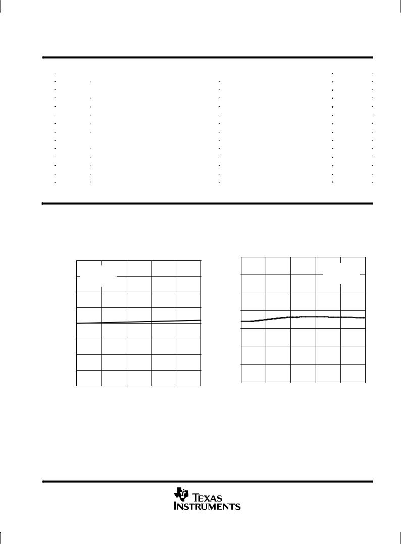
Figure 1 |
Figure 2 |
POST OFFICE BOX 655303 •DALLAS, TEXAS 75265 |
9 |
TPS70745, TPS70748, TPS70751, TPS70758, TPS70702 DUAL-OUTPUT LOW-DROPOUT VOLTAGE REGULATORS
WITH POWER UP SEQUENCING FOR SPLIT VOLTAGE DSP SYSTEMS
SLVS291 ± MAY 2000
VO ± Output Voltage ± V
TYPICAL CHARACTERISTICS
|
|
TPS70745 |
|
|
|
|
|
OUTPUT VOLTAGE |
|
||
|
|
|
vs |
|
|
|
|
OUTPUT CURRENT |
|
||
1.201 |
|
|
|
|
|
|
|
|
|
VIN2 = 2.7 V |
|
|
|
|
|
TJ = 25°C |
|
1.200 |
|
|
|
VOUT2 |
|
1.199 |
|
|
|
|
|
1.198 |
|
|
|
|
|
1.197 |
|
|
|
|
|
1.196 |
|
|
|
|
|
1.195 |
|
|
|
|
|
0 |
0.025 |
0.05 |
0.075 |
0.1 |
0.125 |
IO ± Output Current ± A
Figure 3
|
|
|
|
|
TPS70751 |
|
|
|
|
|
|
|
|
|
TPS70751 |
|
|
|
|
||||
|
|
|
OUTPUT VOLTAGE |
|
|
|
|
|
|
OUTPUT VOLTAGE |
|
|
|
||||||||||
|
|
|
|
|
vs |
|
|
|
|
|
|
|
|
|
|
vs |
|
|
|
|
|
||
|
|
JUNCTION TEMPERATURE |
|
|
|
|
JUNCTION TEMPERATURE |
|
|
||||||||||||||
|
3.35 |
|
|
|
|
|
|
|
|
|
|
|
3.35 |
|
|
|
|
|
|
|
|
|
|
|
|
VIN1 = 4.3 V |
|
|
|
|
|
|
|
|
|
|
VIN1 = 4.3 V |
|
|
|
|
|
|
|
|
||
|
|
IO = 1 mA |
|
|
|
|
|
|
|
|
|
|
|
IO = 250 mA |
|
|
|
|
|
|
|
|
|
|
3.33 |
VOUT1 |
|
|
|
|
|
|
|
|
|
|
3.33 |
VOUT1 |
|
|
|
|
|
|
|
|
|
± V |
3.31 |
|
|
|
|
|
|
|
|
|
|
± V |
3.31 |
|
|
|
|
|
|
|
|
|
|
Voltage |
|
|
|
|
|
|
|
|
|
|
Voltage |
|
|
|
|
|
|
|
|
|
|
||
3.29 |
|
|
|
|
|
|
|
|
|
|
3.29 |
|
|
|
|
|
|
|
|
|
|
||
± Output |
|
|
|
|
|
|
|
|
|
|
± Output |
|
|
|
|
|
|
|
|
|
|
||
3.27 |
|
|
|
|
|
|
|
|
|
|
3.27 |
|
|
|
|
|
|
|
|
|
|
||
O |
|
|
|
|
|
|
|
|
|
|
O |
|
|
|
|
|
|
|
|
|
|
||
|
|
|
|
|
|
|
|
|
|
|
|
|
|
|
|
|
|
|
|
|
|
||
V |
|
|
|
|
|
|
|
|
|
|
|
V |
|
|
|
|
|
|
|
|
|
|
|
|
3.25 |
|
|
|
|
|
|
|
|
|
|
|
3.25 |
|
|
|
|
|
|
|
|
|
|
|
3.23 |
|
|
|
|
|
|
|
|
|
|
|
3.23 |
|
|
|
|
|
|
|
|
|
|
|
±40 ±25 ±10 |
5 |
20 |
35 |
50 |
65 |
80 |
95 |
110 |
125 |
|
±40 ±25 ±10 |
5 |
20 |
35 |
50 |
65 |
80 |
95 |
110 |
125 |
||
|
|
TJ ± Junction Temperature ± °C |
|
|
|
|
TJ ± Junction Temperature ± °C |
|
|
||||||||||||||
|
|
|
|
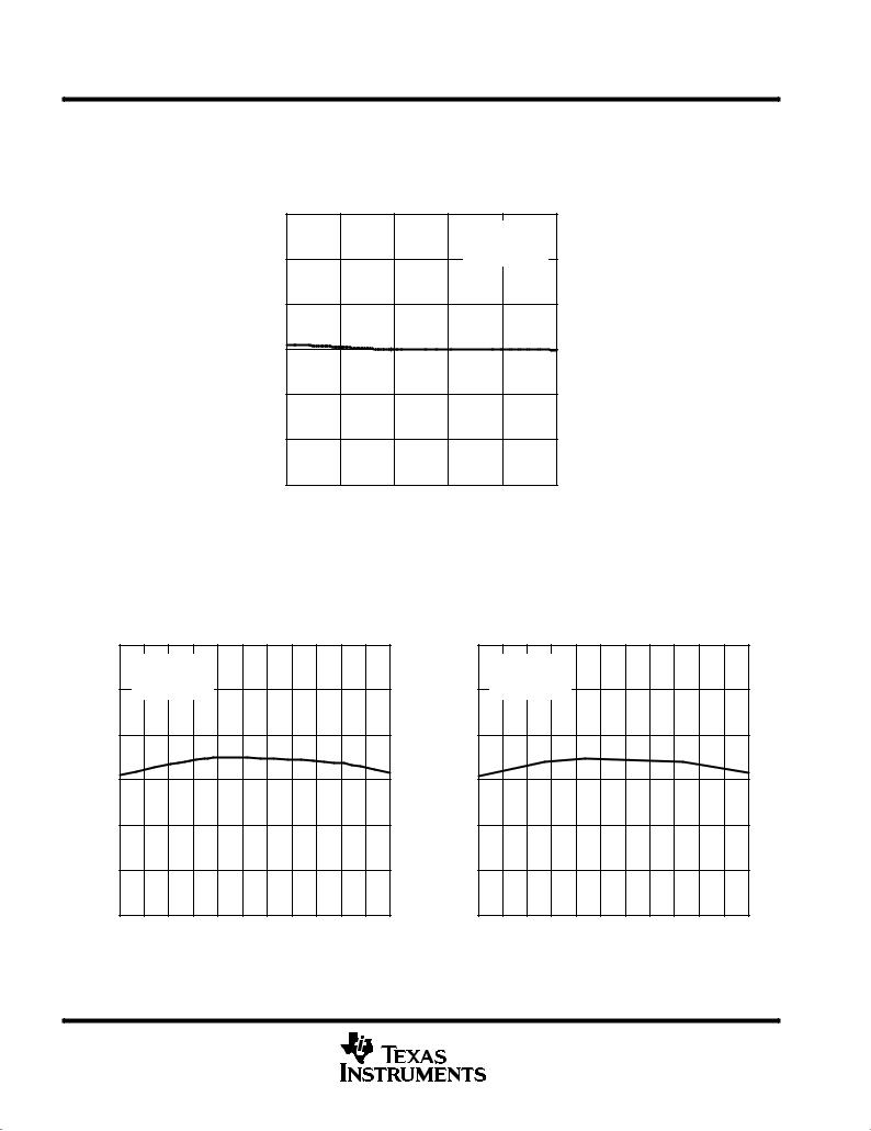
Figure 4 |
|
|
|
|
|
|
|
|
|
Figure 5 |
|
|
|
|
|
||||
10 |
POST OFFICE BOX 655303 •DALLAS, TEXAS 75265 |

TPS70745, TPS70748, TPS70751, TPS70758, TPS70702 DUAL-OUTPUT LOW-DROPOUT VOLTAGE REGULATORS WITH POWER UP SEQUENCING FOR SPLIT VOLTAGE DSP SYSTEMS
SLVS291 ± MAY 2000
TYPICAL CHARACTERISTICS
|
|
|
|
|
TPS70751 |
|
|
|
|
|
|
|
|
TPS70751 |
|
|
|
|
|
|||
|
|
|
OUTPUT VOLTAGE |
|
|
|
|
|
OUTPUT VOLTAGE |
|
|
|
||||||||||
|
|
|
|
|
vs |
|
|
|
|
|
|
|
|
|
vs |
|
|
|
|
|
|
|
|
|
JUNCTION TEMPERATURE |
|
|
|
JUNCTION TEMPERATURE |
|
|
||||||||||||||
|
1.800 |
|
|
|
|
|
|
|
|
|
|
1.799 |
|
|
|
|
|
|
|
|
|
|
|
|
VIN2 = 2.8 V |
|
|
|
|
|
|
|
|
|
VIN2 = 2.8 V |
|
|
|
|
|
|
|
|
||
|
1.798 |
IO = 1 mA |
|
|
|
|
|
|
|
|
|
1.798 |
IO = 125 mA |
|
|
|
|
|
|
|
|
|
|
VOUT2 |
|
|
|
|
|
|
|
|
|
|
VOUT2 |
|
|
|
|
|
|
|
|
|
|
|
|
|
|
|
|
|
|
|
|
|
|
1.797 |
|
|
|
|
|
|
|
|
|
|
V |
1.796 |
|
|
|
|
|
|
|
|
|
V |
|
|
|
|
|
|
|
|
|
|
|
± |
|
|
|
|
|
|
|
|
|
± |
1.796 |
|
|
|
|
|
|
|
|
|
|
|
|
|
|
|
|
|
|
|
|
|
|
|
|
|
|
|
|
|
|
|
|||
Voltage |
|
|
|
|
|
|
|
|
|
|
Voltage |
|
|
|
|
|
|
|
|
|
|
|
1.794 |
|
|
|
|
|
|
|
|
|
1.795 |
|
|
|
|
|
|
|
|
|
|
||
|
|
|
|
|
|
|
|
|
|
|
|
|
|
|
|
|
|
|
|
|||
|
|
|
|
|
|
|
|
|
|
|
|
|
|
|
|
|
|
|
|
|
||
± Output |
1.792 |
|
|
|
|
|
|
|
|
|
± Output |
1.794 |
|
|
|
|
|
|
|
|
|
|
|
|
|
|
|
|
|
|
|
|
|
|
|
|
|
|
|
|
|
|
|||
|
|
|
|
|
|
|
|
|
|
1.793 |
|
|
|
|
|
|
|
|
|
|
||
O |
1.790 |
|
|
|
|
|
|
|
|
|
O |
|
|
|
|
|
|
|
|
|
|
|
V |
|
|
|
|
|
|
|
|
|
V |
|
|
|
|
|
|
|
|
|
|
|
|
|
|
|
|
|
|
|
|
|
|
1.792 |
|
|
|
|
|
|
|
|
|
|
||
|
|
|
|
|
|
|
|
|
|
|
|
|
|
|
|
|
|
|
|
|
|
|
|
1.788 |
|
|
|
|
|
|
|
|
|
|
1.791 |
|
|
|
|
|
|
|
|
|
|
|
|
|
|
|
|
|
|
|
|
|
|
|
|
|
|
|
|
|
|
|
|
|
|
1.786 |
|
|
|
|
|
|
|
|
|
|
1.790 |
|
|
|
|
|
|
|
|
|
|
|
±40 ±25 ±10 |
5 |
20 |
35 |
50 |
65 |
80 |
95 |
110 |
125 |
±40 ±25 ±10 |
5 |
20 |
35 |
50 |
65 |
80 |
95 |
110 |
125 |
||
|
|
TJ ± Junction Temperature ± °C |
|
|
|
TJ ± Junction Temperature ± °C |
|
|
||||||||||||||
|
|
|
|
Figure 6 |
|
|
|
|
|
|
|
|
|
Figure 7 |
|
|
|
|
|
|||
|
|
|
|
|
|
|
|
|
|
GROUND CURRENT |
|
|
|
|
|
|
|
|
|
|
||
|
|
|
|
|
|
|
|
|
|
|
vs |
|
|
|
|
|
|
|
|
|
|
|
JUNCTION TEMPERATURE
210
Regulator 1 and Regulator 2
|
200 |
|
|
|
|
|
|
|
|
|
|
|
IOUT1 = 1 mA |
|
|
|
|
|
|
||
A |
190 |
IOUT2 = 1 mA |
|
|
|
|
|
|
||
± |
|
|
|
|
|
|
|
|
|
|
Current |
180 |
|
|
|
|
|
|
|
|
|
|
|
|
|
|
|
|
|
|
|
|
Ground |
170 |
|
|
|
IOUT1 = 250 mA |
|
|
|||
|
|
|
|
IOUT2 = 125 mA |
|
|
||||
|
160 |
|
|
|
|
|
|
|
|
|
|
150 |
|
|
|
|
|
|
|
|
|
|
±40 ±25 ±10 |
5 |
20 |
35 |
50 |
65 |
80 |
95 |
110 |
125 |
|
TJ ± Junction Temperature ± °C |
|
|
|||||||
Figure 8
POST OFFICE BOX 655303 •DALLAS, TEXAS 75265 |
11 |
 Loading...