


 Loading...
Texas Instruments TPS61020DRC, TPS61024DRC, TPS61025DRC, TPS61026DRC, TPS61027DRC Schematic [ru]
...TPS61020, |
TPS61024, |
TPS61025 |
TPS61026, |
TPS61027, TPS61028 |
|
|
(3,25 mm x 3,25 mm) |
TPS61029 |
www.ti.com |
|
|
|
SLVS451D – SEPTEMBER 2003 – REVISED FEBRUARY 2006 |
|
|
|
96% EFFICIENT SYNCHRONOUS BOOST CONVERTER
FEATURES
∙96% Efficient Synchronous Boost Converter
∙Output Voltage Remains Regulated When Input Voltage Exceeds Nominal Output Voltage
∙Device Quiescent Current: 25 µA (Typ)
∙Input Voltage Range: 0.9 V to 6.5 V
∙Fixed and Adjustable Output Voltage Options Up to 5.5 V
∙Power Save Mode for Improved Efficiency at Low Output Power
∙Low Battery Comparator
∙Low EMI-Converter (Integrated Antiringing Switch)
∙Load Disconnect During Shutdown
∙Over-Temperature Protection
∙Small 3 mm × 3 mm QFN-10 Package
APPLICATIONS
∙All One-Cell, Two-Cell and Three-Cell Alkaline, NiCd or NiMH or Single-Cell Li Battery Powered Products
∙Portable Audio Players
∙PDAs
∙Cellular Phones
∙Personal Medical Products
∙Camera White LED Flash Light
DESCRIPTION
The TPS6102x devices provide a power supply solution for products powered by either a one-cell, two-cell, or three-cell alkaline, NiCd or NiMH, or one-cell Li-Ion or Li-polymer battery. Output currents can go as high as 200 mA while using a single-cell alkaline, and discharge it down to 0.9 V. It can also be used for generating 5 V at 500 mA from a 3.3-V rail or a Li-Ion battery. The boost converter is based on a fixed frequency, pulse-width-modulation (PWM) controller using a synchronous rectifier to obtain maximum efficiency. At low load currents the converter enters the Power Save mode to maintain a high efficiency over a wide load current range. The Power Save mode can be disabled, forcing the converter to operate at a fixed switching frequency. The maximum peak current in the boost switch is limited to a value of 800 mA, 1500 mA or 1800mA depending on the device version.
The TPS6102x devices keep the output voltage regulated even when the input voltage exceeds the nominal output voltage. The output voltage can be programmed by an external resistor divider, or is fixed internally on the chip. The converter can be disabled to minimize battery drain. During shutdown, the load is completely disconnected from the battery. A low-EMI mode is implemented to reduce ringing and, in effect, lower radiated electromagnetic energy when the converter enters the discontinuous conduction mode. The device is packaged in a 10-pin QFN PowerPAD™ package measuring 3 mm x 3 mm (DRC).
|
|
L1 |
|
|
|
|
|
|
|
|
|
6.8 μH |
SW |
VOUT |
|
|
|
|
|
|
|
|
|
C2 |
|
C3 |
|||
|
|
|
VBAT |
|
|
||||
|
|
|
R3 |
2.2 |
μ |
F |
47 |
μ |
|
|
|
|
|
|
F |
||||
0.9-V To |
C1 |
R1 |
EN |
FB |
|
|
|
|
|
6.5-V Input |
10 μF |
|
LBI |
R4 |
|
|
|
|
R5 |
|
|
|
|
|
|
|
|||
|
|
R2 |
|
|
|
|
|
|
|
|
|
|
PS |
LBO |
|
|
|
|
|
|
|
|
|
|
|
|
|
|
|
|
|
|
GND |
PGND |
|
|
|
|
|
|
|
|
|
TPS61020 |
|
|
|
|
|
VO
3.3 V Up To
200 mA
Low Battery
Output
Please be aware that an important notice concerning availability, standard warranty, and use in critical applications of Texas Instruments semiconductor products and disclaimers thereto appears at the end of this data sheet.
PowerPAD is a trademark of Texas Instruments.
PRODUCTION DATA information is current as of publication date. |
Copyright © 2003–2006, Texas Instruments Incorporated |
Products conform to specifications per the terms of the Texas |
|
Instruments standard warranty. Production processing does not |
|
necessarily include testing of all parameters. |
|

TPS61020, TPS61024, TPS61025
TPS61026, TPS61027, TPS61028
TPS61029
www.ti.com
SLVS451D – SEPTEMBER 2003 – REVISED FEBRUARY 2006
These devices have limited built-in ESD protection. The leads should be shorted together or the device placed in conductive foam during storage or handling to prevent electrostatic damage to the MOS gates.
AVAILABLE OUTPUT VOLTAGE OPTIONS(1)
|
OUTPUT |
NOMINAL SWITCH |
PACKAGE |
|
PART NUMBER(2) |
T |
VOLTAGE |
PACKAGE |
|||
A |
DC/DC |
CURRENT LIMIT |
MARKING |
|
|
|
|
|
|
|
|
|
Adjustable |
1500 mA |
BDR |
|
TPS61020DRC |
|
Adjustable |
800 mA |
BNE |
|
TPS61028DRC |
|
Adjustable |
1800 mA |
BRF |
|
TPS61029DRC |
–40°C to 85°C |
3.0 V |
1500 mA |
BDS |
10-Pin QFN |
TPS61024DRC |
|
3.3 V |
1500 mA |
BDT |
|
TPS61025DRC |
|
5 V |
1800 mA |
BRD |
|
TPS61026DRC |
|
5 V |
1500 mA |
BDU |
|
TPS61027DRC |
(1)Contact the factory to check availability of other fixed output voltage versions.
(2)The DRC package is available taped and reeled. Add R suffix to device type (e.g., TPS61020DRCR) to order quantities of 3000 devices per reel. Add a T suffix to the device type (i.e., TPS61020DRCT) to order quantities of 250 devices per reel.
ABSOLUTE MAXIMUM RATINGS
over operating free-air temperature range (unless otherwise noted)(1)
|
TPS6102x |
Input voltage range on SW, VOUT, LBO, VBAT, PS, EN, FB, LBI |
–0.3 V to 7 V |
Operating virtual junction temperature range, TJ |
–40°C to 150°C |
Storage temperature range, Tstg |
–65°C to 150°C |
(1)Stresses beyond those listed under absolute maximum ratings may cause permanent damage to the device. These are stress ratings only, and functional operation of the device at these or any other conditions beyond those indicated under recommended operating conditions is not implied. Exposure to absolute-maximum-rated conditions for extended periods may affect device reliabilitiy.
DISSIPATION RATINGS TABLE
PACKAGE |
THERMAL RESISTANCE |
POWER RATING |
DERATING FACTOR ABOVE |
|
ΘJA |
TA≤ 25°C |
TA = 25°C |
||
|
||||
DRC |
48.7°C/W |
2054 mW |
21 mW/°C |
RECOMMENDED OPERATING CONDITIONS
|
MIN |
NOM MAX |
UNIT |
Supply voltage at VBAT, VI (TPS61020, TPS61024, TPS61025, TPS61028) |
0.9 |
6.5 |
V |
Supply voltage at VBAT, VI (TPS61026, TPS61029) |
0.9 |
5.5 |
V |
Operating free air temperature range, TA |
–40 |
85 |
°C |
Operating virtual junction temperature range, TJ |
–40 |
125 |
°C |
2 |
Submit Documentation Feedback |

TPS61020, TPS61024, TPS61025 TPS61026, TPS61027, TPS61028
TPS61029
www.ti.com
SLVS451D – SEPTEMBER 2003 – REVISED FEBRUARY 2006
ELECTRICAL CHARACTERISTICS
over recommended free-air temperature range and over recommended input voltage range (typical at an ambient temperature range of 25°C) (unless otherwise noted)
 DC/DC STAGE
|
PARAMETER |
|
Minimum input voltage for start-up |
|
Input voltage range, after start-up (TPS61020, |
VI |
TPS61024, TPS61025, TPS61027, TPS61028) |
|
Input voltage range, after start-up (TPS61026, |
|
TPS61029) |
VO |
TPS61020, TPS61028 and TPS61029 output |
voltage range |
|
VFB |
TPS61020, TPS61028 and TPS61029 feedback |
voltage |
|
f |
Oscillator frequency |
ISW |
Switch current limit (TPS61020, TPS61024, |
TPS61025, TPS61027) |
|
ISW |
Switch current limit (TPS61028) |
ISW |
Switch current limit (TPS61026, TPS61029) |
|
Start-up current limit |
|
SWN switch on resistance |
|
SWP switch on resistance |
|
Total accuracy (including line and load regulation) |
|
Line regulation |
|
Load regulation |
|
VBAT |
|
Quiescent current |
|
VOUT |
|
Shutdown current |
CONTROL STAGE |
|
|
PARAMETER |
VUVLO |
Under voltage lockout threshold |
VIL |
LBI voltage threshold |
|
LBI input hysteresis |
|
LBI input current |
VOL |
LBO output low voltage |
Vlkg |
LBO output leakage current |
VIL |
EN, PS input low voltage |
VIH |
EN, PS input high voltage |
|
EN, PS input current |
|
Overtemperature protection |
|
Overtemperature hysteresis |
TEST CONDITIONS |
MIN |
TYP |
MAX |
UNIT |
RL = 120 Ω |
|
0.9 |
1.2 |
V |
|
0.9 |
|
6.5 |
V |
|
0.9 |
|
5.5 |
V |
|
1.8 |
|
5.5 |
V |
|
490 |
500 |
510 |
mV |
|
480 |
600 |
720 |
kHz |
VOUT= 3.3 V |
1200 |
1500 |
1800 |
mA |
VOUT= 3.3 V |
|
800 |
|
mA |
VOUT= 3.3 V |
1500 |
1800 |
2100 |
mA |
|
|
0.4 x ISW |
|
mA |
VOUT= 3.3 V |
|
260 |
|
mΩ |
VOUT= 3.3 V |
|
290 |
|
mΩ |
|
|
|
±3% |
|
|
|
|
0.6% |
|
|
|
|
0.6% |
|
IO = 0 mA, VEN = VBAT = 1.2 V, |
|
1 |
3 |
µA |
VOUT = 3.3 V, TA = 25°C |
|
25 |
45 |
µA |
VEN = 0 V, VBAT = 1.2 V, |
|
0.1 |
1 |
µA |
TA = 25°C |
|
|
|
|
TEST CONDITIONS |
MIN |
TYP |
MAX |
UNIT |
VLBI voltage decreasing |
|
0.8 |
|
V |
VLBI voltage decreasing |
490 |
500 |
510 |
mV |
|
|
10 |
|
mV |
EN = VBAT or GND |
|
0.01 |
0.1 |
µA |
VO = 3.3 V, IOI = 100 µA |
|
0.04 |
0.4 |
V |
VLBO = 7 V |
|
0.01 |
0.1 |
µA |
|
|
|
0.2 × VBAT |
V |
|
0.8 × VBAT |
|
|
V |
Clamped on GND or VBAT |
|
0.01 |
0.1 |
µA |
|
|
140 |
|
°C |
|
|
20 |
|
°C |
Submit Documentation Feedback |
3 |

TPS61020, TPS61024, TPS61025
TPS61026, TPS61027, TPS61028
TPS61029
www.ti.com
SLVS451D – SEPTEMBER 2003 – REVISED FEBRUARY 2006
PIN ASSIGNMENTS
|
DRC PACKAGE |
|
(TOP VIEW) |
EN |
PGND |
VOUT |
SW |
FB |
PS |
LBO |
LBI |
GND |
VBAT |
|
|
|
Terminal Functions |
|
TERMINAL |
I/O |
DESCRIPTION |
||
NAME |
NO. |
|||
|
|
|||
EN |
1 |
I |
Enable input. (1/VBAT enabled, 0/GND disabled) |
|
FB |
3 |
I |
Voltage feedback of adjustable versions |
|
GND |
5 |
|
Control / logic ground |
|
LBI |
7 |
I |
Low battery comparator input (comparator enabled with EN), may not be left floating, should be connected to |
|
|
|
|
GND or VBAT if comparator is not used |
|
LBO |
4 |
O |
Low battery comparator output (open drain) |
|
PS |
8 |
I |
Enable/disable power save mode (1/VBAT disabled, 0/GND enabled) |
|
SW |
9 |
I |
Boost and rectifying switch input |
|
PGND |
10 |
|
Power ground |
|
VBAT |
6 |
I |
Supply voltage |
|
VOUT |
2 |
O |
Boost converter output |
|
PowerPAD™ |
|
|
Must be soldered to achieve appropriate power dissipation. Should be connected to PGND. |
|
4 |
Submit Documentation Feedback |
TPS61020, TPS61024, TPS61025 TPS61026, TPS61027, TPS61028
TPS61029
www.ti.com
SLVS451D – SEPTEMBER 2003 – REVISED FEBRUARY 2006
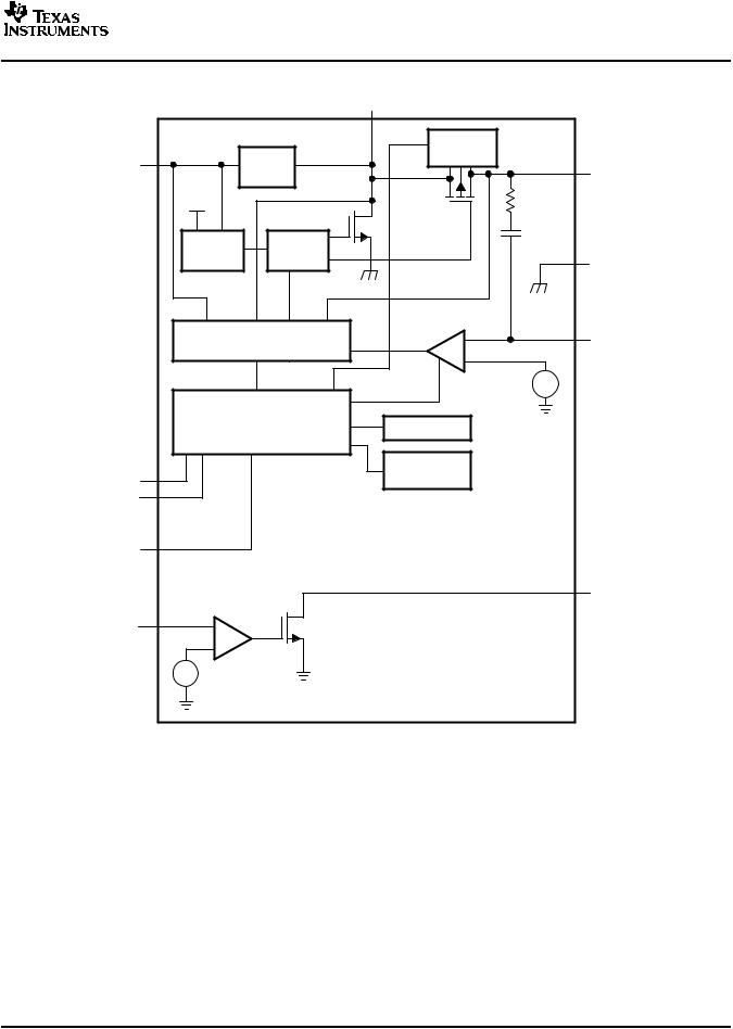
FUNCTIONAL BLOCK DIAGRAM (TPS61020, TPS61028, TPS61029)
|
|
|
SW |
|
|
|
|
|
Backgate |
|
|
VBAT |
Anti- |
Control |
|
||
|
|
|
|||
Ringing |
|
|
VOUT |
||
|
|
|
|||
VOUT |
|
|
10 kΩ |
||
|
|
|
|
||
|
Vmax |
Gate |
|
|
20 pF |
|
|
|
|
||
|
Control |
Control |
|
|
PGND |
|
|
|
|
|
|
|
|
|
PGND |
|
|
|
|
|
Error |
|
PGND |
|
|
|
|
|
|
|
Regulator |
Amplifier |
_ |
FB |
|
|
|
|
|||
|
|
|
|
+ |
|
|
|
|
|
|
+ |
|
|
|
|
Vref = 0.5 V |
_ |
|
Control Logic |
|
GND |
||
|
Oscillator |
|
|
||
|
|
|
|
|
|
|
|
|
Temperature |
|
|
EN |
|
|
Control |
|
|
|
|
|
|
|
|
PS |
|
|
|
|
|
GND |
|
|
|
|
|
|
Low Battery |
|
|
|
LDO |
|
|
|
|
|
|
|
Comparator |
|
|
|
|
LBI |
_ |
|
|
|
|
|
|
|
|
|
|
|
+ |
|
|
|
|
+ |
Vref = 0.5 V |
|
|
|
|
_ |
|
|
|
|
|
|
GND |
|
|
|
|
Submit Documentation Feedback |
5 |

TPS61020, TPS61024, TPS61025
TPS61026, TPS61027, TPS61028
TPS61029
www.ti.com
SLVS451D – SEPTEMBER 2003 – REVISED FEBRUARY 2006
PARAMETER MEASUREMENT INFORMATION
|
|
L1 |
|
|
|
|
|
|
|
|
|
6.8 μH |
SW |
VOUT |
|
|
|
|
|
|
|
|
|
C2 |
|
C3 |
|||
|
|
|
VBAT |
|
|
||||
|
|
|
R3 |
2.2 |
μ |
F |
47 |
μ |
|
|
|
|
|
|
F |
||||
Power |
C1 |
R1 |
EN |
FB |
|
|
|
|
|
Supply |
10 μF |
|
LBI |
R4 |
|
|
|
|
R5 |
|
|
|
|
|
|
|
|||
|
|
R2 |
|
|
|
|
|
|
|
|
|
|
PS |
LBO |
|
|
|
|
|
|
|
|
|
|
|
|
|
|
|
List of Components: |
|
GND |
PGND |
|
|
|
|
|
|
|
|
TPS6102x |
|
|
|
|
|
||
U1 = TPS6102xDRC |
|
|
|
|
|
|
|
|
|
|
|
|
|
|
|
|
|
|
|
L1 = EPCOS B82462−G4682 |
|
|
|
|
|
|
|
|
|
C1, C2 = X7R/X5R Ceramic |
|
|
|
|
|
|
|
|
|
C3 = Low ESR Tantalum |
|
|
|
|
|
|
|
|
|
VCC
Boost Output
Control Output
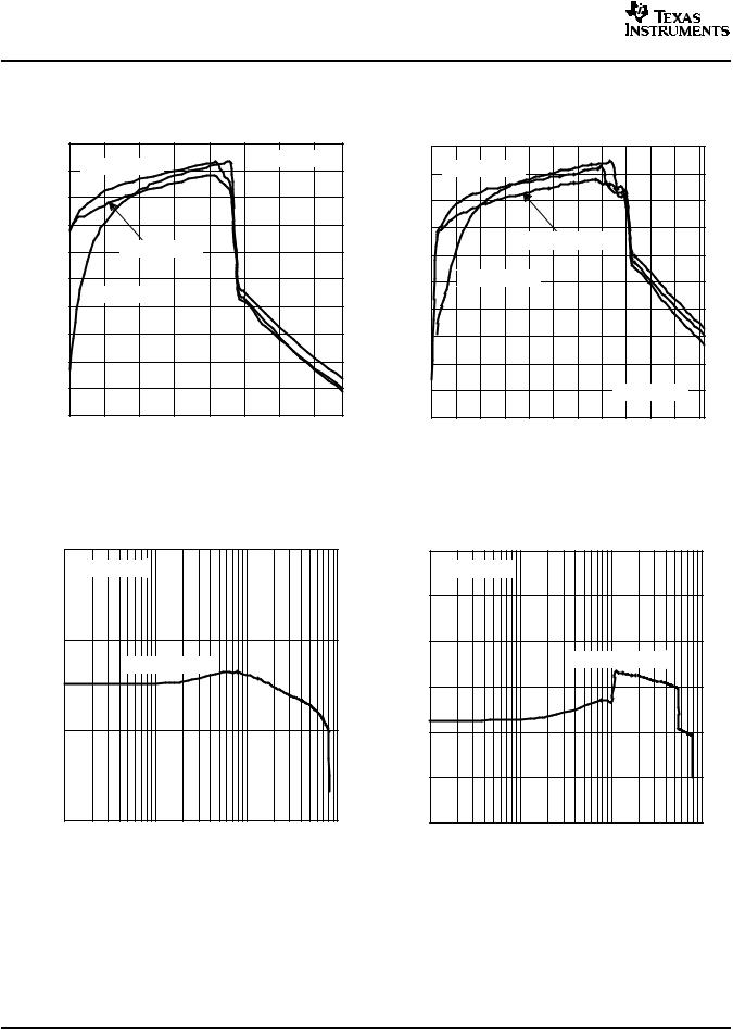
TYPICAL CHARACTERISTICS
Table of Graphs
|
|
FIGURE |
|
Maximum output current |
vs Input voltage |
1 |
|
|
vs Output current (TPS61020) |
2 |
|
|
vs Output current (TPS61025) |
3 |
|
Efficiency |
vs Output current (TPS61027) |
4 |
|
|
vs Input voltage (TPS61025) |
5 |
|
|
vs Input voltage (TPS61027) |
6 |
|
Output voltage |
vs Output current (TPS61025) |
7 |
|
vs Output current (TPS61027) |
8 |
||
|
|||
No load supply current into VBAT |
vs Input voltage |
9 |
|
No load supply current into VOUT |
vs Input voltage |
10 |
|
|
Output voltage in continuous mode (TPS61025) |
11 |
|
|
Output voltage in continuous mode (TPS61027) |
12 |
|
|
Output voltage in power save mode (TPS61025) |
13 |
|
|
Output voltage in power save mode (TPS61027) |
14 |
|
Waveforms |
Load transient response (TPS61025) |
15 |
|
Load transient response (TPS61027) |
16 |
||
|
|||
|
Line transient response (TPS61025) |
17 |
|
|
Line transient response (TPS61027) |
18 |
|
|
Start-up after enable (TPS61025) |
19 |
|
|
Start-up after enable (TPS61027) |
20 |
6 |
Submit Documentation Feedback |

TPS61020, TPS61024, TPS61025 TPS61026, TPS61027, TPS61028
TPS61029
www.ti.com
|
SLVS451D – SEPTEMBER 2003 – REVISED FEBRUARY 2006 |
MAXIMUM OUTPUT CURRENT |
TPS61020 |
vs |
EFFICIENCY |
INPUT VOLTAGE |
vs |
|
OUTPUT CURRENT |
|
1400 |
|
|
|
|
|
|
|
100 |
|
|
|
|
|
|
|
|
|
|
|
|
90 |
VBAT = 0.9 V |
|
VO = 1.8 V |
|
|
|
|
|
|
|
|
|
|
|
||
|
1200 |
|
|
|
|
|
|
|
|
|
|
|
|
|
|
|
|
|
|
|
|
|
|
|
|
- mA |
|
VO = 3.3 V |
|
VO = 5 V |
|
80 |
|
|
|
|||
1000 |
|
|
|
|
|
|
|
70 |
|
|
|
|
Current |
|
|
|
|
|
|
|
|
|
|
||
|
|
|
|
|
|
|
|
VBAT = 1.8 V |
|
|
||
|
|
|
|
|
|
|
|
|
|
|
||
800 |
|
|
|
|
|
|
- % |
60 |
|
|
|
|
Maximum Output |
|
|
|
|
|
|
|
Efficiency |
50 |
|
|
|
600 |
|
|
|
|
|
|
40 |
|
|
|
||
|
|
|
|
|
|
|
|
|
|
|||
400 |
|
|
VO = 1.8 V |
|
|
|
30 |
|
|
|
||
|
|
|
|
|
|
|
20 |
|
|
|
||
|
200 |
|
|
|
|
|
|
|
|
|
|
|
|
|
|
|
|
|
|
|
|
|
|
|
|
|
|
|
|
|
|
|
|
|
10 |
|
|
|
|
0 |
|
|
|
|
|
|
|
0 |
|
|
|
|
0.9 |
1.7 |
2.5 |
3.3 |
4.1 |
4.9 |
5.7 |
6.5 |
|
|
|
|
|
1 |
10 |
100 |
1000 |
||||||||
|
|
|
VI - Input Voltage - V |
|
|
|
||||||
|
|
|
|
|
|
|
IO - Output Current - mA |
|
||||
|
|
|
|
Figure 1. |
|
|
|
|
Figure 2. |
|
|
|
TPS61025 |
TPS61027 |
EFFICIENCY |
EFFICIENCY |
vs |
vs |
OUTPUT CURRENT |
OUTPUT CURRENT |
|
100 |
|
|
|
100 |
|
|
|
|
|
90 |
|
|
|
90 |
|
|
|
|
|
80 |
VBAT = 2.4 V |
|
80 |
|
|
|
|
|
|
|
|
|
VBAT = 1.2 V |
|
|
|
||
|
70 |
|
VBAT = 1.8 V |
|
70 |
VBAT = 2.4 V |
|
||
|
|
|
|
|
|||||
% |
60 |
|
|
% |
60 |
VBAT = 1.8 V |
VBAT = 3.6 V |
|
|
- |
|
|
|
- |
|
|
|
|
|
Efficiency |
50 |
|
VBAT = 0.9 V |
Efficiency |
50 |
|
|
|
|
|
|
|
|
|
|
|
|||
|
|
|
|
|
|
|
|
|
|
|
40 |
|
|
|
40 |
|
|
|
|
|
30 |
|
|
|
30 |
|
|
|
|
|
20 |
|
|
|
20 |
|
|
|
|
|
10 |
|
|
VO = 3.3 V |
10 |
|
|
VO = 5 V |
|
|
0 |
10 |
100 |
1000 |
0 |
10 |
|
100 |
1000 |
|
1 |
1 |
|
||||||
|
|
IO - Output Current - mA |
|
|
IO - Output Current - mA |
|
|||
|
|
|
Figure 3. |
|
|
|
Figure 4. |
|
|
Submit Documentation Feedback |
7 |
TPS61020, TPS61024, TPS61025
TPS61026, TPS61027, TPS61028
TPS61029
www.ti.com
SLVS451D – SEPTEMBER 2003 – REVISED FEBRUARY 2006 |
|
TPS61025 |
TPS61027 |
EFFICIENCY |
EFFICIENCY |
vs |
vs |
INPUT VOLTAGE |
INPUT VOLTAGE |
|
100 |
|
|
|
|
|
|
|
|
|
95 |
IO = 100 mA |
|
|
|
VO = 3.3 V |
|
||
|
|
|
|
|
|
|
|||
|
90 |
|
|
|
|
|
|
|
|
|
85 |
|
|
|
|
|
|
|
|
% |
80 |
|
IO = 10 mA |
|
|
|
|
|
|
- |
|
|
|
|
|
|
|
|
|
Efficiency |
75 |
|
|
|
|
|
|
|
|
70 |
IO = 250 mA |
|
|
|
|
|
|
||
|
|
|
|
|
|
|
|
||
|
|
|
|
|
|
|
|
|
|
|
65 |
|
|
|
|
|
|
|
|
|
60 |
|
|
|
|
|
|
|
|
|
55 |
|
|
|
|
|
|
|
|
|
50 |
|
|
|
|
|
|
|
|
|
0.9 |
1.4 |
1.9 |
2.4 |
2.9 |
3.4 |
3.9 |
4.4 |
4.9 |
|
|
|
VI - Input Voltage - V |
|
|
|
|||
|
100 |
|
|
|
|
|
|
|
|
|
|
|
|
95 |
IO = 100 mA |
|
|
|
|
|
|
|
|
||
|
90 |
|
|
|
|
|
|
|
|
|
|
|
|
85 |
|
|
|
|
|
|
|
|
|
|
|
% |
80 |
|
|
|
IO = 10 mA |
|
|
|
|
|
||
|
|
|
|
|
|
|
|
|
|
|
||
- |
|
|
|
|
|
|
|
|
|
|
|
|
Efficiency |
75 |
IO = 250 mA |
|
|
|
|
|
|
|
|||
70 |
|
|
|
|
|
|
|
|
|
|
|
|
|
|
|
|
|
|
|
|
|
|
|
|
|
|
65 |
|
|
|
|
|
|
|
|
|
|
|
|
60 |
|
|
|
|
|
|
|
|
|
|
|
|
55 |
|
|
|
|
|
|
|
VO = 5 V |
|
|
|
|
|
|
|
|
|
|
|
|
|
|
||
|
50 |
|
|
|
|
|
|
|
|
|
|
|
|
0.9 |
1.4 |
1.9 |
2.4 |
2.9 |
3.4 |
3.9 |
4.4 |
4.9 |
5.4 |
5.9 |
6.4 |
|
|
|
|
VI - Input Voltage - V |
|
|
|
|
||||
Figure 5. |
Figure 6. |
TPS61025 |
TPS61027 |
OUTPUT VOLTAGE |
OUTPUT VOLTAGE |
vs |
vs |
OUTPUT CURRENT |
OUTPUT CURRENT |
|
3.35 |
|
|
|
5.10 |
|
|
VO = 3.3 V |
|
|
|
|
|
|
|
|
5.05 |
- V |
3.30 |
|
|
- V |
5 |
Voltage |
|
|
Voltage |
||
|
VBAT = 2.4 V |
|
|
||
|
|
|
4.95 |
||
- Output |
|
|
|
- Output |
|
3.25 |
|
|
4.90 |
||
O |
|
|
O |
||
|
|
|
|
||
V |
|
|
|
V |
|
|
|
|
|
|
4.85 |
|
3.20 |
|
|
|
4.80 |
|
1 |
10 |
100 |
1000 |
|
|
|
IO - Output Current - mA |
|
|
|
|
VO = 5 V |
|
|
|
|
VBAT = 3.6 V |
|
1 |
10 |
100 |
1000 |
|
IO - Output Current - mA |
|
|
Figure 7. |
Figure 8. |
8 |
Submit Documentation Feedback |
www.ti.com
NO LOAD SUPPLY CURRENT INTO VBAT vs
INPUT VOLTAGE
|
1.6 |
|
|
|
|
|
|
|
|
|
|
|
μ A |
|
|
|
|
|
TA = 85°C |
|
|
|
|
|
|
1.4 |
|
|
|
|
|
|
|
|
|
|
|
|
- |
|
|
|
|
|
|
|
|
|
|
|
|
VBAT |
1.2 |
|
|
|
|
|
|
|
|
|
|
|
|
|
|
|
|
|
|
|
|
|
|
|
|
Into |
1 |
|
|
|
|
|
|
|
|
|
|
|
Current |
0.8 |
|
|
|
|
|
|
|
TA = -40°C |
|
|
|
|
|
|
|
|
TA = 25°C |
|
|
|
||||
Supply |
0.6 |
|
|
|
|
|
|
|
|
|
||
|
|
|
|
|
|
|
|
|
|
|
||
|
|
|
|
|
|
|
|
|
|
|
|
|
No Load |
0.4 |
|
|
|
|
|
|
|
|
|
|
|
0.2 |
|
|
|
|
|
|
|
|
|
|
|
|
|
|
|
|
|
|
|
|
|
|
|
|
|
|
0 |
|
|
|
|
|
|
|
|
|
|
|
|
0.9 |
1.5 |
2 |
2.5 |
3 |
3.5 |
4 |
4.5 |
5 |
5.5 |
6 |
6.5 |
|
|
|
|
VI - Input Voltage - V |
|
|
|
|
||||
Figure 9.
TPS61025
OUTPUT VOLTAGE IN CONTINUOUS MODE
|
VI = 1.2 V, |
VoltageOutput |
RL = 33 Ω, |
mV/div20 |
|
|
VO = 3.3 V |
Inductor Current |
200 mA/div |
t - Time - 1 μs/div
Figure 11.
TPS61020, TPS61024, TPS61025
TPS61026, TPS61027, TPS61028
TPS61029
SLVS451D – SEPTEMBER 2003 – REVISED FEBRUARY 2006
NO LOAD SUPPLY CURRENT INTO VOUT vs
INPUT VOLTAGE
|
34.8 |
|
|
|
|
|
|
|
TA = 85°C |
|
|
|
- μA |
|
|
|
|
|
|
|
|
|
|
||
29.8 |
|
|
|
|
|
|
|
|
|
|
|
|
VOUT |
24.8 |
|
TA = -40°C |
|
|
|
|
|
|
|
||
Into |
|
|
|
|
|
|
|
|
||||
|
|
|
|
|
TA = 25°C |
|
|
|||||
|
|
|
|
|
|
|
|
|
|
|||
Current |
19.8 |
|
|
|
|
|
|
|
|
|
|
|
|
|
|
|
|
|
|
|
|
|
|
|
|
Supply |
14.8 |
|
|
|
|
|
|
|
|
|
|
|
9.8 |
|
|
|
|
|
|
|
|
|
|
|
|
No Load |
|
|
|
|
|
|
|
|
|
|
|
|
4.8 |
|
|
|
|
|
|
|
|
|
|
|
|
|
-0.2 |
|
|
|
|
|
|
|
|
|
|
|
|
0.9 |
1.5 |
2 |
2.5 |
3 |
3.5 |
4 |
4.5 |
5 |
5.5 |
6 |
6.5 |
|
|
|
|
VI - Input Voltage - V |
|
|
|
|
||||
Figure 10.
TPS61027
OUTPUT VOLTAGE IN CONTINUOUS MODE
Output Voltage |
20 mV/div |
|
Inductor Current |
200 mA/div |
VI = 3.6 V, |
|
|
RL = 25 Ω, |
|
|
VO = 5 V |
t - Time - 1 μs/div
Figure 12.
Submit Documentation Feedback |
9 |
Loading...