


TMX320C6203GLS
Texas Instruments TMX320C6203GLS, TMX320C6203GJL, TMX320C6202GLS, TMX320C6202GJL, TMS320C6202GLS200 Datasheet
...
TMS320C6202, TMS320C6202B, TMS320C6203, TMS320C6204
FIXED-POINT DIGITAL SIGNAL PROCESSORS
SPRS104A – OCTOBER 1999 – REVISED MARCH 2000
1
POST OFFICE BOX 1443 • HOUSTON, TEXAS 77251–1443
D Highest Performance Fixed-Point Digital
Signal Processors (DSPs) TMS320C62x
– 5-, 4-, 3.33-ns Instruction Cycle Time
– 200-, 250-, 300-MHz Clock Rate
– Eight 32-Bit Instructions/Cycle
– 1600, 2000, 2400 MIPS
D VelociTI Advanced Very Long Instruction
Word (VLIW) ’C62x CPU Core
– Eight Highly Independent Functional
Units:
– Six ALUs (32-/40-Bit)
– Two 16-Bit Multipliers (32-Bit Result)
– Load-Store Architecture With 32 32-Bit
General-Purpose Registers
– Instruction Packing Reduces Code Size
– All Instructions Conditional
D Instruction Set Features
– Byte-Addressable (8-, 16-, 32-Bit Data)
– 8-Bit Overflow Protection
– Saturation
– Bit-Field Extract, Set, Clear
– Bit-Counting
– Normalization
D On-Chip SRAM
– 1M-Bit (’C6204)
– 3M-Bit (’C6202/’C6202B)
– 7M-Bit (’C6203)
D 32-Bit External Memory Interface (EMIF)
– Glueless Interface to Synchronous
Memories: SDRAM or SBSRAM
– Glueless Interface to Asynchronous
Memories: SRAM and EPROM
– 52M-Byte Addressable External Memory
Space
D Four-Channel Bootloading
Direct-Memory-Access (DMA) Controller
With an Auxiliary Channel
D Flexible Phase-Locked-Loop (PLL) Clock
Generator
D 32-Bit Expansion Bus
– Glueless/Low-Glue Interface to Popular
PCI Bridge Chips
– Glueless/Low-Glue Interface to Popular
Synchronous or Asynchronous
Microprocessor Buses
– Master/Slave Functionality
– Glueless Interface to Synchronous FIFOs
and Asynchronous Peripherals
D Multichannel Buffered Serial Ports
(McBSPs)
– Direct Interface to T1/E1, MVIP, SCSA
Framers
– ST-Bus-Switching Compatible
– Up to 256 Channels Each
– AC97-Compatible
– Serial-Peripheral Interface (SPI)
Compatible (Motorola)
D Two 32-Bit General-Purpose Timers
D IEEE-1149.1 (JTAG
†
)
Boundary-Scan-Compatible
D 352-Pin BGA Package (GJL) (’02/02B/03)
D 384-Pin BGA Package (GLS) (’02/02B/03)
D 340-Pin BGA Package (GLW) (’C6204 only)
– Pin-Compatible With the GLS Package
Except Inner Row of Balls (Additional
Power and Ground Pins) are Removed
‡
D 0.18-µm/5-Level Metal Process (’6202 only)
0.15-µm/5-Level Metal Process (’02B/03/04)
– CMOS Technology
D 3.3-V I/Os, 1.8-V Internal (’C6202 only)
3.3-V I/Os, 1.5-V Internal (’C6202B/03/04)
PR
O
DU
C
T PREVIEW
This document contains information on products in more than one phase
of development. The status of each device is indicated on the page(s)
specifying its electrical characteristics.
Please be aware that an important notice concerning availability, standard warranty, and use in critical applications of
Texas Instruments semiconductor products and disclaimers thereto appears at the end of this data sheet.
VelociTI is a trademark of Texas Instruments Incorporated.
Motorola is a trademark of Motorola, Inc.
†
IEEE Standard 1149.1-1990 Standard-Test-Access Port and Boundary Scan Architecture.
‡
For more details, see the GLS/GLW BGA package bottom view.
Copyright 2000, Texas Instruments Incorporated
TMS320C6202, TMS320C6202B, TMS320C6203, TMS320C6204
FIXED-POINT DIGITAL SIGNAL PROCESSORS
SPRS104A – OCTOBER 1999 – REVISED MARCH 2000
2
POST OFFICE BOX 1443 • HOUSTON, TEXAS 77251–1443
Table of Contents
input and output clocks 35. . . . . . . . . . . . . . . . . . . . . . . . . . .
asynchronous memory timing 38. . . . . . . . . . . . . . . . . . . . .
synchronous-burst memory timing 41. . . . . . . . . . . . . . . . .
synchronous DRAM timing 43. . . . . . . . . . . . . . . . . . . . . . . .
HOLD/HOLDA timing 47. . . . . . . . . . . . . . . . . . . . . . . . . . . .
reset timing 48. . . . . . . . . . . . . . . . . . . . . . . . . . . . . . . . . . . . .
external interrupt timing 50. . . . . . . . . . . . . . . . . . . . . . . . . .
expansion bus synchronous FIFO timing 51. . . . . . . . . . . .
expansion bus asynchronous peripheral timing 53. . . . . .
expansion bus synchronous host port timing 56. . . . . . . .
expansion bus asynchronous host port timing 62. . . . . . .
XHOLD/XHOLDA timing 64. . . . . . . . . . . . . . . . . . . . . . . . . .
multichannel buffered serial port timing 66. . . . . . . . . . . . .
DMAC, timer, power-down timing 78. . . . . . . . . . . . . . . . . .
JTAG test-port timing 80. . . . . . . . . . . . . . . . . . . . . . . . . . . .
mechanical data 81. . . . . . . . . . . . . . . . . . . . . . . . . . . . . . . . .
GJL/GLS/GLW BGA packages (bottom view) 3. . . . . . . . . .
device selection guide 4. . . . . . . . . . . . . . . . . . . . . . . . . . . . . .
description 5. . . . . . . . . . . . . . . . . . . . . . . . . . . . . . . . . . . . . . .
’C62x device compatibility 6. . . . . . . . . . . . . . . . . . . . . . . . . .
functional and CPU block diagram (’C62x devices) 7. . . . .
CPU description 8. . . . . . . . . . . . . . . . . . . . . . . . . . . . . . . . . . .
signal groups description 10. . . . . . . . . . . . . . . . . . . . . . . . . .
signal descriptions 13. . . . . . . . . . . . . . . . . . . . . . . . . . . . . . . .
development support 24. . . . . . . . . . . . . . . . . . . . . . . . . . . . . .
documentation support 28. . . . . . . . . . . . . . . . . . . . . . . . . . . .
clock PLL 29. . . . . . . . . . . . . . . . . . . . . . . . . . . . . . . . . . . . . . .
power-supply sequencing 31. . . . . . . . . . . . . . . . . . . . . . . . . .
absolute maximum ratings over operating case
temperature range 32. . . . . . . . . . . . . . . . . . . . . . . . . . .
recommended operating conditions 32. . . . . . . . . . . . . . . . .
electrical characteristics over recommended ranges
of supply voltage and operating case temperature 33
parameter measurement information 34. . . . . . . . . . . . . . . .
PR
O
DU
C
T PREVIEW
TMS320C6202, TMS320C6202B, TMS320C6203, TMS320C6204
FIXED-POINT DIGITAL SIGNAL PROCESSORS
SPRS104A – OCTOBER 1999 – REVISED MARCH 2000
3
POST OFFICE BOX 1443 • HOUSTON, TEXAS 77251–1443
GJL/GLS/GLW BGA packages (bottom view)
22
19
20
17
16
18
13
14
11
10
12
15
AA
U
W
N
R
8
7
5
4
6
J
L
E
G
2
1
A
C
3 9 21
B
D
F
H
K
M
P
T
V
Y
AB
GLS 384-PIN BGA PACKAGE (’C6202/02B/03 ONLY)
GLW 340-PIN BGA PACKAGE (’C6204 ONLY)
(BOTTOM VIEW)
GJL 352-PIN BALL GRID ARRAY (BGA) PACKAGE (’C6202/02B/03 ONLY)
(BOTTOM VIEW)
AF
AD
AB
AA
AC
W
Y
U
V
AE
R
N
P
L
H
J
K
M
F
G
D
E
B
A
C
T
25
2622
23
20
19 211715
1612
13
14 1810
9
8
75
64
3
2
111
24
These balls are
NOT
applicable for the ’C6204 devices GLW 340-pin BGA package.
PR
O
DU
C
T PREVIEW
TMS320C6202, TMS320C6202B, TMS320C6203, TMS320C6204
FIXED-POINT DIGITAL SIGNAL PROCESSORS
SPRS104A – OCTOBER 1999 – REVISED MARCH 2000
4
POST OFFICE BOX 1443 • HOUSTON, TEXAS 77251–1443
device selection guide
Table 1 provides an overview of the TMS320C6202/02B/03/04 pin-compatible DSPs. The table shows
significant features of each device, including the capacity of on-chip RAM, the peripherals, the execution time,
and the package type with pin count, etc.
T able 1. TMS320C6202/02B/03/04 DSP Selection Guide
HARDWARE FEATURES ’C6202 ’C6202B ’C6203 ’C6204
EMIF √ √ √ √
p
DMA 4-Channel
4-Channel With
Throughput
Enhancements
4-Channel With
Throughput
Enhancements
4-Channel With
Throughput
Enhancements
Peripherals
Expansion Bus √ √ √ √
McBSPs 3 3 3 2
32-Bit Timers 2 2 2 2
Size (Bytes) 256K 256K 384K 64K
Internal Program
Memory
Organization
Block 0:
128K Bytes
Mapped Program
Block 1:
128K Bytes
Cache/Mapped
Program
Block 0:
128K Bytes
Mapped Program
Block 1:
128K Bytes
Cache/Mapped
Program
Block 0:
256K Bytes Mapped
Program
Block 1:
128K Bytes
Cache/Mapped
Program
1 Block:
64K Bytes
Cache/Mapped
Program
Size (Bytes) 128K 128K 512K 64K
Internal Data
Memory
Organization
2 Blocks:
Four 16-Bit Banks
per Block
50/50 Split
2 Blocks:
Four 16-Bit Banks
per Block
50/50 Split
2 Blocks:
Four 16-Bit Banks
per Block
50/50 Split
2 Blocks:
Four 16-Bit Banks
per Block
50/50 Split
Frequency MHz 200, 250 250 250, 300 200
Cycle Time ns
4 ns (’6202-250)
5 ns (’6202-200)
4 ns (’6202B-250)
3.33 ns (’6203-300)
4 ns (’6203-250)
5 ns (’6204-200)
Core (V) 1.8 1.5 1.5 1.5
Voltage
I/O (V) 3.3 3.3 3.3 3.3
Bypass (x1) √ √ √ √
PLL Options:
x4 √ √ √ √
PLL
O tions:
In Both Packages
x8 – √ √ –
g
x10 – √ √ –
Additional
x6 – √ √ –
Additional
PLL Options:
x7 – √ √ –
18 x 18 mm
x9 – √ √ –
Packages
(GLS/GLW only)
x11 – √ √ –
27 x 27 mm 352-pin GJL 352-pin GJL 352-pin GJL –
BGA Package
18 x 18 mm 384-pin GLS 384-pin GLS 384-pin GLS 340-pin GLW
Process
Technology
µm 0.18 µm (18C05) 0.15 µm (15C05) 0.15 µm (15C05) 0.15 µm (15C05)
Product Status
Product Preview (PP)
Advance Information (AI)
Production Data (PD)
PD PP AI PP
PR
O
DU
C
T PREVIEW

TMS320C6202, TMS320C6202B, TMS320C6203, TMS320C6204
FIXED-POINT DIGITAL SIGNAL PROCESSORS
SPRS104A – OCTOBER 1999 – REVISED MARCH 2000
5
POST OFFICE BOX 1443 • HOUSTON, TEXAS 77251–1443
description
The TMS320C6202, TMS320C6202B, TMS320C6203, and TMS320C6204 devices are part of the
TMS320C62x fixed-point DSP family in the TMS320C6000 platform. The ’C62x devices are based on the
high-performance, advanced VelociTI very-long-instruction-word (VLIW) architecture developed by Texas
Instruments (TI), making these DSPs an excellent choice for multichannel and multifunction applications.
The TMS320C62x DSP offers cost-effective solutions to high-performance DSP programming challenges. The
TMS320C6202B/’03 has a performance of up to 2400 million instructions per second (MIPS) at 300 MHz, while
the TMS320C6202 has a performance of up to 2000 MIPS at 250 MHz, and the TMS320C6204 has a
performance of up to 1600 MIPS at 200 MHz. The ’C6202/’02B/’03/’04 DSP possesses the operational flexibility
of high-speed controllers and the numerical capability of array processors. These processors have
32 general-purpose registers of 32-bit word length and eight highly independent functional units. The eight
functional units provide six arithmetic logic units (ALUs) for a high degree of parallelism and two 16-bit multipliers
for a 32-bit result. The ’C6202/’02B/’03/’04 can produce two multiply-accumulates (MACs) per cycle. This gives
a total of 600 million MACs per second (MMACS) for the ’C6202B/’03 device, a total of 500 MMACS for the
’C6202 device, and a total of 400 MMACS for the ’C6204 device. The ’C6202/’02B/’03/’04 DSP also has
application-specific hardware logic, on-chip memory, and additional on-chip peripherals.
The TMS320C62x DSPs include an on-chip memory, with the ’C6203 device offering the most memory at
7 Mbits. For the ’C6202/’02B device, program memory consists of two blocks, with a 128K-byte block configured
as memory-mapped program space, and the other 128K-byte block user-configurable as cache or
memory-mapped program space. Data memory consists of two 64K-byte blocks of RAM. Similarly , the ’C6203
device program memory consists of two blocks, with a 256K-byte block configured as memory-mapped program
space, and the other 128K-byte block user-configurable as cache or memory-mapped program space. Data
memory consists of two 256K-byte blocks of RAM. For the ’C6204 device, program memory consists of a single
64K-byte block that is user-configured as cache or memory-mapped program space. Data memory consists of
two 32K-byte blocks of RAM.
The ’C6202/’02B/’03/’04 device has a powerful and diverse set of peripherals. The peripheral set includes
multichannel buffered serial ports (McBSPs), general-purpose timers, a 32-bit expansion bus (XB) that offers
ease of interface to synchronous or asynchronous industry-standard host bus protocols, and a glueless 32-bit
external memory interface (EMIF) capable of interfacing to SDRAM or SBSRAM and asynchronous peripherals.
The ’C62x devices have a complete set of development tools which includes: a new C compiler, an assembly
optimizer to simplify programming and scheduling, and a Windows debugger interface for visibility into source
code execution.
PR
O
DU
C
T PREVIEW
Windows is a registered trademark of the Microsoft Corporation.

TMS320C6202, TMS320C6202B, TMS320C6203, TMS320C6204
FIXED-POINT DIGITAL SIGNAL PROCESSORS
SPRS104A – OCTOBER 1999 – REVISED MARCH 2000
6
POST OFFICE BOX 1443 • HOUSTON, TEXAS 77251–1443
’C62x device compatibility
The TMS320C6202, ’C6202B, ’C6203, and ’C6204 devices are pin-compatible; thus, making new system
designs easier and providing faster time to market. The following list summarizes the ’C62x device characteristic
differences:
D Core Supply Voltage (1.8 V versus 1.5 V)
D PLL Options Availability
Table 1 identifies the available PLL multiply factors [e.g., CLKIN x1 (PLL bypassed), x4] for each of the
’C62x devices. For additional details on the PLL clock module, see the Clock PLL section of this data sheet.
D On-Chip Memory Size
The ’C6202/’02B, ’C6203, and ’C6204 devices have different on-chip program memory and data memory
sizes (see Table 1).
D McBSPs
The ’C6204 device has two McBSPs while the ’C6202/’02B/’03 devices have three McBSPs on-chip.
For a more detailed discussion on migration concerns, and similarities/differences between the ’C6202,
’C6202B, ’C6203, and ’C6204 devices, see the
How to Begin Development and Migrate Across the
TMS320C6202/6202B/6203/6204 DSPs
application report (literature number SPRA603) document.
PR
O
DU
C
T PREVIEW
TMS320C6202, TMS320C6202B, TMS320C6203, TMS320C6204
FIXED-POINT DIGITAL SIGNAL PROCESSORS
SPRS104A – OCTOBER 1999 – REVISED MARCH 2000
7
POST OFFICE BOX 1443 • HOUSTON, TEXAS 77251–1443
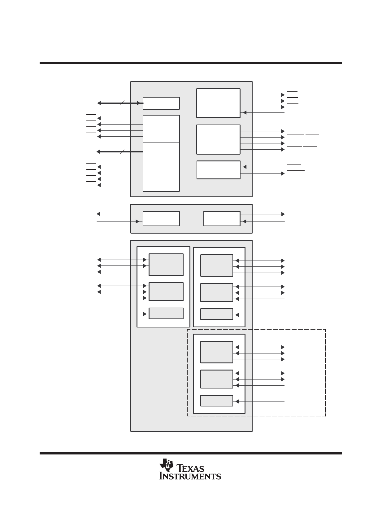
functional and CPU block diagram (’C62x devices)
Direct Memory
Access Controller
(DMA)
(see Table 1)
Test
’C62x CPU
Data Path B
B Register File
Program
Access/Cache
Controller
Instruction Fetch
Instruction Dispatch
Instruction Decode
Data Path A
A Register File
PLL
(see Table 1)
Data
Access
Controller
Power-
Down
Logic
.L1 .S1 .M1 .D1 .D2 .M2 .S2 .L2
32
SDRAM or
SBSRAM
ROM/FLASH
SRAM
I/O Devices
32
Synchronous
FIFOs
I/O Devices
Timer 0
Timer 1
External Memory
Interface (EMIF)
Multichannel
Buffered Serial
Port 0
Multichannel
Buffered Serial
Port 1
Multichannel
Buffered Serial
Port 2
†
Expansion
Bus
Internal Program Memory
(see Table 1)
Control
Registers
Control
Logic
Internal Data
Memory
(see Table 1)
In-Circuit
Emulation
Interrupt
Control
Framing Chips:
H.100, MVIP ,
SCSA, T1, E1
AC97 Devices,
SPI Devices,
Codecs
HOST CONNECTION
Master /Slave
TI PCI2040
Power PC
683xx
960
’C6202/’02B/’03/’04 Digital Signal Processors
†
McBSP2 is
not
applicable for the ’C6204 device.
Program
DMA Buses
Data Bus
Bus
PR
O
DU
C
T PREVIEW

TMS320C6202, TMS320C6202B, TMS320C6203, TMS320C6204
FIXED-POINT DIGITAL SIGNAL PROCESSORS
SPRS104A – OCTOBER 1999 – REVISED MARCH 2000
8
POST OFFICE BOX 1443 • HOUSTON, TEXAS 77251–1443
CPU description
The CPU fetches VelociTI advanced very-long instruction words (VLIW) (256 bits wide) to supply up to eight
32-bit instructions to the eight functional units during every clock cycle. The VelociTI VLIW architecture features
controls by which all eight units do not have to be supplied with instructions if they are not ready to execute. The
first bit of every 32-bit instruction determines if the next instruction belongs to the same execute packet as the
previous instruction, or whether it should be executed in the following clock as a part of the next execute packet.
Fetch packets are always 256 bits wide; however, the execute packets can vary in size. The variable-length
execute packets are a key memory-saving feature, distinguishing the ’C62x CPU from other VLIW architectures.
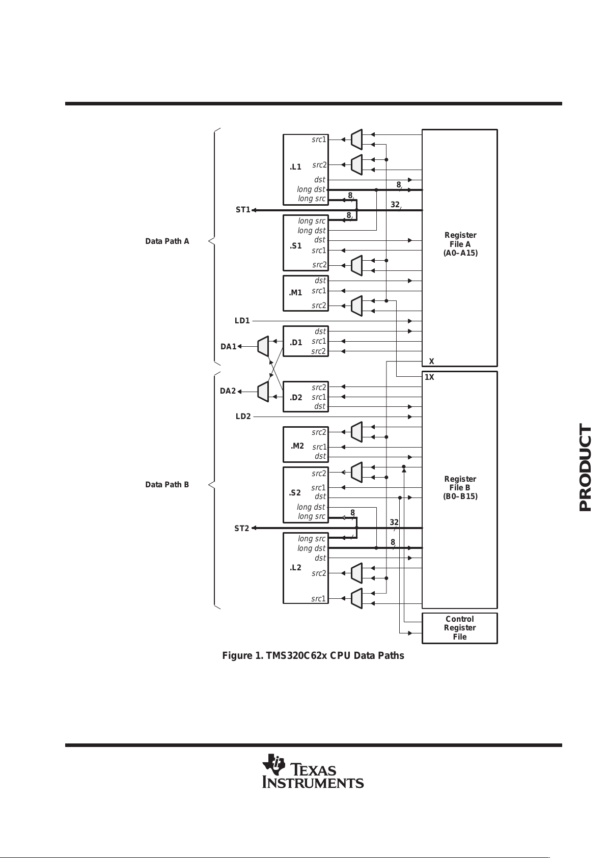
The CPU features two sets of functional units. Each set contains four units and a register file. One set contains
functional units .L1, .S1, .M1, and .D1; the other set contains units .D2, .M2, .S2, and .L2. The two register files
each contain 16 32-bit registers for a total of 32 general-purpose registers. The two sets of functional units, along
with two register files, compose sides A and B of the CPU (see the Functional and CPU Block Diagram and
Figure 1). The four functional units on each side of the CPU can freely share the 16 registers belonging to that
side. Additionally , each side features a single data bus connected to all the registers on the other side, by which
the two sets of functional units can access data from the register files on the opposite side. While register access
by functional units on the same side of the CPU as the register file can service all the units in a single clock cycle,
register access using the register file across the CPU supports one read and one write per cycle.
Another key feature of the ’C62x CPU is the load/store architecture, where all instructions operate on registers
(as opposed to data in memory). Two sets of data-addressing units (.D1 and .D2) are responsible for all data
transfers between the register files and the memory. The data address driven by the .D units allows data
addresses generated from one register file to be used to load or store data to or from the other register file. The
’C62x CPU supports a variety of indirect addressing modes using either linear- or circular-addressing modes
with 5- or 15-bit offsets. All instructions are conditional, and most can access any one of the 32 registers. Some
registers, however, are singled out to support specific addressing or to hold the condition for conditional
instructions (if the condition is not automatically “true”). The two .M functional units are dedicated for multiplies.
The two .S and .L functional units perform a general set of arithmetic, logical, and branch functions with results
available every clock cycle.
The processing flow begins when a 256-bit-wide instruction fetch packet is fetched from a program memory.
The 32-bit instructions destined for the individual functional units are “linked” together by “1” bits in the least
significant bit (LSB) position of the instructions. The instructions that are “chained” together for simultaneous
execution (up to eight in total) compose an execute packet. A “0” in the LSB of an instruction breaks the chain,
effectively placing the instructions that follow it in the next execute packet. If an execute packet crosses the
fetch-packet boundary (256 bits wide), the assembler places it in the next fetch packet, while the remainder of
the current fetch packet is padded with NOP instructions. The number of execute packets within a fetch packet
can vary from one to eight. Execute packets are dispatched to their respective functional units at the rate of one
per clock cycle and the next 256-bit fetch packet is not fetched until all the execute packets from the current fetch
packet have been dispatched. After decoding, the instructions simultaneously drive all active functional units
for a maximum execution rate of eight instructions every clock cycle. While most results are stored in 32-bit
registers, they can be subsequently moved to memory as bytes or half-words as well. All load and store
instructions are byte-, half-word, or word-addressable.
PR
O
DU
C
T PREVIEW
TMS320C6202, TMS320C6202B, TMS320C6203, TMS320C6204
FIXED-POINT DIGITAL SIGNAL PROCESSORS
SPRS104A – OCTOBER 1999 – REVISED MARCH 2000
9
POST OFFICE BOX 1443 • HOUSTON, TEXAS 77251–1443
CPU description (continued)
8
8
2X
1X
.L2
.S2
.M2
.D2
.D1
.M1
.S1
.L1
long src
dst
src
2
src
1
src
1
src
1
src
1
src
1
src
1
src
1
src
1
8
8
8
8
long dst
long dst
dst
dst
dst
dst
dst
dst
dst
src
2
src
2
src
2
src
2
src
2
src
2
src
2
long src
DA1
DA2
ST1
LD1
LD2
ST2
32
32
Register
File A
(A0–A15)
long src
long dst
long dst
long src
Data Path B
Data Path A
Register
File B
(B0–B15)
Control
Register
File
Figure 1. TMS320C62x CPU Data Paths
PR
O
DU
C
T PREVIEW

TMS320C6202, TMS320C6202B, TMS320C6203, TMS320C6204
FIXED-POINT DIGITAL SIGNAL PROCESSORS
SPRS104A – OCTOBER 1999 – REVISED MARCH 2000
10
POST OFFICE BOX 1443 • HOUSTON, TEXAS 77251–1443
signal groups description
TRST
EXT_INT7
Clock/PLL
IEEE Standard
1149.1
(JTAG)
Emulation
Reserved
‡
Reset and
Interrupts
DMA Status
Power-Down
Status
Control/Status
TDI
TDO
TMS
TCK
CLKIN
CLKOUT1
CLKMODE0
PLLV
PLLG
PLLF
EMU1
EMU0
RSV2
RSV1
RSV0
NMI
IACK
INUM3
INUM2
INUM1
INUM0
DMAC3
DMAC2
DMAC1
DMAC0
PD
RSV4
EXT_INT6
EXT_INT5
EXT_INT4
RESET
CLKOUT2
CLKMODE1
†
CLKMODE2
†
†
CLKMODE1 is NOT available on the ’C6202 device GJL package.
CLKMODE2 is NOT available on the GJL packages for the ’C6202/’02B/’03 devices.
RSV7
RSV6
RSV5
RSV9
RSV8
RSV11
RSV10
’C6204
Only
RSV3
‡
RSV5 through RSV11 pins are used on the ’C6204 device only.
Figure 2. CPU Signals
PR
O
DU
C
T PREVIEW
TMS320C6202, TMS320C6202B, TMS320C6203, TMS320C6204
FIXED-POINT DIGITAL SIGNAL PROCESSORS
SPRS104A – OCTOBER 1999 – REVISED MARCH 2000
11
POST OFFICE BOX 1443 • HOUSTON, TEXAS 77251–1443
signal groups description (continued)
CE3
ARE
ED[31:0]
CE2
CE1
CE0
EA[21:2]
BE3
BE2
BE1
BE0
HOLD
HOLDA
TOUT1
CLKX1
FSX1
DX1
CLKR1
FSR1
DR1
CLKS1
AOE
AWE
ARDY
SDA10
SDRAS
/SSOE
SDCAS/SSADS
SDWE/SSWE
TOUT0
CLKX2
FSX2
DX2
CLKR2
FSR2
DR2
CLKS2
Data
Memory Map
Space Select
Word Address
Byte Enables
HOLD/
HOLDA
32
20
Asynchronous
Memory
Control
Synchronous
Memory
Control
EMIF
(External Memory Interface)
Timer 1
Transmit
Transmit
Timer 0
Timers
McBSP1
McBSP2
Receive
Receive
Clock
Clock
McBSPs
(Multichannel Buffered Serial Ports)
TINP1
TINP0
CLKX0
FSX0
DX0
CLKR0
FSR0
DR0
CLKS0
Transmit
McBSP0
Receive
Clock
N/A For ’C6204 Devices
Figure 3. Peripheral Signals
PR
O
DU
C
T PREVIEW

TMS320C6202, TMS320C6202B, TMS320C6203, TMS320C6204
FIXED-POINT DIGITAL SIGNAL PROCESSORS
SPRS104A – OCTOBER 1999 – REVISED MARCH 2000
12
POST OFFICE BOX 1443 • HOUSTON, TEXAS 77251–1443
signal groups description (continued)
XD[31:0]
XBE2
/XA4
XBE1
/XA3
XBE0
/XA2
XRDY
XHOLD
XHOLDA
XFCLK
XCLKIN
XOE
XRE
Data
Byte-Enable
Control/
Address
Control
Arbitration
32
Clocks
I/O Port
Control
Expansion Bus
XWE/XWAIT
XCE3
XCE2
XCE1
XCE0
XCS
XAS
Host
Interface
Control
XCNTL
XW/R
XBLAST
XBOFF
XBE3/XA5
Figure 3. Peripheral Signals (Continued)
PR
O
DU
C
T PREVIEW
TMS320C6202, TMS320C6202B, TMS320C6203, TMS320C6204
FIXED-POINT DIGITAL SIGNAL PROCESSORS
SPRS104A – OCTOBER 1999 – REVISED MARCH 2000
13
POST OFFICE BOX 1443 • HOUSTON, TEXAS 77251–1443
Signal Descriptions
SIGNAL
PIN NO.
SIGNAL
NAME
GJL GLS GLW
†
TYPE
‡
DESCRIPTION
CLOCK/PLL
CLKIN C12 B10 B10 I Clock Input
CLKOUT1 AD20 Y18 Y18 O Clock output at full device speed
CLKOUT2 AC19 AB19 AB19 O
Clock output at half of device speed
• Used for synchronous memory interface
CLKMODE0 B15 B12 B12 I
Clock mode selects
p
p
CLKMODE1 C11
§
A9
¶
A9
¶
I
• Selects what multiply factors of the input clock frequency the CPU frequency
equals.
CLKMODE2 – A14
¶
A14
¶
I
For more detail on CLKMODE pins and the PLL multiply factors, see the Clock
PLL section of this data sheet.
PLLV
#
D13 C11 C11 A
||
PLL analog V
CC
connection for the low-pass filter
PLLG
#
D14 C12 C12 A
||
PLL analog GND connection for the low-pass filter
PLLF
#
C13 A11 A11 A
||
PLL low-pass filter connection to external components and a bypass capacitor
JTAG EMULATION
TMS AD7 Y5 Y5 I JTAG test-port mode select (features an internal pullup)
TDO AE6 AA4 AA4 O/Z JTAG test-port data out
TDI AF5 Y4 Y4 I JTAG test-port data in (features an internal pullup)
TCK AE5 AB2 AB2 I JT AG test-port clock
TRST AC7 AA3 AA3 I JTAG test-port reset (features an internal pulldown)
EMU1 AF6 AA5 AA5 I/O/Z Emulation pin 1, pullup with a dedicated 20-kΩ resistor
k
EMU0 AC8 AB4 AB4 I/O/Z Emulation pin 0, pullup with a dedicated 20-kΩ resistor
k
RESET AND INTERRUPTS
RESET K2 J3 J3 I Device reset
NMI L2 K2 K2 I
Nonmaskable interrupt
• Edge-driven (rising edge)
EXT_INT7 V4 U2 U2
EXT_INT6 Y2 U3 U3
External interrupts
EXT_INT5 AA1 W1 W1
I
External
interru ts
• Edge-driven (rising edge)
EXT_INT4 W4 V2 V2
ggg
IACK Y1 V1 V1 O Interrupt acknowledge for all active interrupts serviced by the CPU
INUM3 V2 R3 R3
INUM2 U4 T1 T1
Active interrupt identification number
p
INUM1 V3 T2 T2
O
• Valid during IACK for all active interrupts (not just external)
• En
c
o
d
in
g
or
de
r follow
s
th
e
int
e
rr
u
pt-
se
rvi
ce
f
e
t
c
h-p
ac
k
e
t or
de
rin
g
INUM0 W2 T3 T3
• Encoding
order
follows
the
interru t
-
service
fetch
-
acket
ordering
†
The GLW BGA package (’C6204 only) is a subset of the GLS package (’C6202/02B/03), with the inner row of core supply voltage (CV
DD
) and
ground (V
SS
) pins removed (see the GLS/GLW BGA package bottom view).
‡
I = Input, O = Output, Z = High Impedance, S = Supply Voltage, GND = Ground
§
For the ’C6202 GJL package only, the C11 pin is ground (V
SS
). For all other ’C62x GJL packages, the C11 pin is CLKMODE1.
¶
For the ’C6202 GLS and ’C6204 GLW packages, the CLKMODE2 (A14) and CLKMODE1 (A9) pins are internally unconnected.
#
PLLV , PLLG, and PLLF are not part of external voltage supply or ground. See the
clock PLL
section for information on how to connect these pins.
||
A = Analog Signal (PLL Filter)
kFor emulation and normal operation, pull up EMU1 and EMU0 with a dedicated 20-kΩ resistor . For boundary scan, pull down EMU1 and EMU0
with a dedicated 20-kΩ resistor.
PR
O
DU
C
T PREVIEW

TMS320C6202, TMS320C6202B, TMS320C6203, TMS320C6204
FIXED-POINT DIGITAL SIGNAL PROCESSORS
SPRS104A – OCTOBER 1999 – REVISED MARCH 2000
14
POST OFFICE BOX 1443 • HOUSTON, TEXAS 77251–1443
Signal Descriptions (Continued)
SIGNAL
PIN NO.
SIGNAL
NAME
GJL GLS GLW
†
TYPE
‡
DESCRIPTION
POWER-DOWN STATUS
PD AB2 Y2 Y2 O Power-down modes 2 or 3 (active if high)
EXPANSION BUS
XCLKIN A9 C8 C8 I Expansion bus synchronous host interface clock input
XFCLK B9 A8 A8 O Expansion bus FIFO interface clock output
XD31 D15 C13 C13
XD30 B16 A13 A13
XD29 A17 C14 C14
XD28 B17 B14 B14
XD27 D16 B15 B15
XD26 A18 C15 C15
XD25 B18 A15 A15
XD24 D17 B16 B16
XD23 C18 C16 C16
XD22 A20 A17 A17
XD21 D18 B17 B17
XD20 C19 C17 C17
Expansion bus data
XD19 A21 B18 B18
• Used for transfer of data, address, and control
• Also controls initialization of DSP modes and expansion bus at reset via pullup/
XD18 D19 A19 A19
• Also
controls
initialization
of
DSP
modes
and
ex ansion
bus
at
reset
via
ullu /
pulldown resistors
XD17 C20 C18 C18
(Note: Reserved boot configuration fields should be pulled down.)
XD16 B21 B19 B19
– XCE
[
3:0
]
memor
y
t
y
pe
XD15 A22 C19 C19
I/O/Z
– XCE[3:0]
memory
ty e
– XBLAST polarity
XD14 D20 B20 B20
y
– XW/R polarity
–
p
XD13 B22 A21 A21
–
A
sync
h
ronous or sync
h
ronous
h
os
t
opera
ti
on
– Arbitration mode (internal or external)
XD12 E25 C21 C21
Arbitration
mode
(internal
or
external)
– FIFO mode
XD11 F24 D20 D20
– Little endian/big endian
–
XD10 E26 B22 B22
–
B
oo
t
mo
d
e
XD9 F25 D21 D21
XD8 G24 E20 E20
XD7 H23 E21 E21
XD6 F26 D22 D22
XD5 G25 F20 F20
XD4 J23 F21 F21
XD3 G26 E22 E22
XD2 H25 G20 G20
XD1 J24 G21 G21
XD0 K23 G22 G22
†
The GLW BGA package (’C6204 only) is a subset of the GLS package (’C6202/02B/03), with the inner row of core supply voltage (CV
DD
) and
ground (V
SS
) pins removed (see the GLS/GLW BGA package bottom view).
‡
I = Input, O = Output, Z = High Impedance, S = Supply Voltage, GND = Ground
PR
O
DU
C
T PREVIEW
TMS320C6202, TMS320C6202B, TMS320C6203, TMS320C6204
FIXED-POINT DIGITAL SIGNAL PROCESSORS
SPRS104A – OCTOBER 1999 – REVISED MARCH 2000
15
POST OFFICE BOX 1443 • HOUSTON, TEXAS 77251–1443
Signal Descriptions (Continued)
SIGNAL
PIN NO.
SIGNAL
NAME
GJL GLS GLW
†
TYPE
‡
DESCRIPTION
EXPANSION BUS (CONTINUED)
XCE3 F2 D2 D2
XCE2 E1 B1 B1
Expansion bus I/O port memory space enables
XCE1 F3 D3 D3
O/Z
• Enabled by bits 28, 29, and 30 of the word address
• Onl
y
one asserted durin
g
an
y
I/O port data access
XCE0 E2 C2 C2
• Only
one
asserted
during
any
I/O
ort
data
access
XBE3/XA5 C7 C5 C5
XBE2/XA4 D8 A4 A4
Expansion bus multiplexed byte-enable control/address signals
p
p
XBE1/XA3 A6 B5 B5
I/O/Z
• Act as byte enable for host port operation
• A
c
t
as
add
r
ess
for I
/O
port op
e
r
a
tion
XBE0/XA2 C8 C6 C6
• Act
as
address
for
I/O
ort
o eration
XOE A7 A6 A6 O/Z Expansion bus I/O port output enable
XRE C9 C7 C7 O/Z Expansion bus I/O port read enable
XWE/XWAIT D10 B7 B7 O/Z Expansion bus I/O port write enable and host port wait signals
XCS A10 C9 C9 I Expansion bus host port chip-select input
XAS D9 B6 B6 I/O/Z Expansion bus host port address strobe
XCNTL B10 B9 B9 I
Expansion bus host control. XCNTL selects between expansion bus address or data
register
XW/R D1 1 B8 B8 I/O/Z Expansion bus host port write/read enable. XW/R polarity selected at reset
XRDY A5 C4 C4 I/O/Z Expansion bus host port ready (active low) and I/O port ready (active high)
XBLAST B6 B4 B4 I/O/Z Expansion bus host port burst last–polarity selected at reset
XBOFF B11 A10 A10 I Expansion bus back off
XHOLD B5 A2 A2 I/O/Z Expansion bus hold request
XHOLDA D7 B3 B3 I/O/Z Expansion bus hold acknowledge
EMIF – CONTROL SIGNALS COMMON TO ALL TYPES OF MEMORY
CE3 AB25 Y21 Y21
CE2 AA24 W20 W20
Memory space enables
CE1 AB26 AA22 AA22
O/Z
• Enabled by bits 24 and 25 of the word address
•
O
nl
y
on
e
asse
rt
ed
du
rin
g
a
n
y
e
xt
e
rn
a
l
da
t
a
access
CE0 AA25 W21 W21
• Only
one
asserted
during
any
external
data
access
BE3 Y24 V20 V20
BE2 W23 V21 V21
B
yte-ena
bl
e contro
l
• Decoded from the two lowest bits of the internal address
BE1 AA26 W22 W22
O/Z
• Decoded
from
the
two
lowest
bits
of
the
internal
address
• Byte-write enables for most types of memory
BE0 Y25 U20 U20
yyy
• Can be directly connected to SDRAM read and write mask signal (SDQM)
†
The GLW BGA package (’C6204 only) is a subset of the GLS package (’C6202/02B/03), with the inner row of core supply voltage (CV
DD
) and
ground (V
SS
) pins removed (see the GLS/GLW BGA package bottom view).
‡
I = Input, O = Output, Z = High Impedance, S = Supply Voltage, GND = Ground
PR
O
DU
C
T PREVIEW
TMS320C6202, TMS320C6202B, TMS320C6203, TMS320C6204
FIXED-POINT DIGITAL SIGNAL PROCESSORS
SPRS104A – OCTOBER 1999 – REVISED MARCH 2000
16
POST OFFICE BOX 1443 • HOUSTON, TEXAS 77251–1443
Signal Descriptions (Continued)
SIGNAL
PIN NO.
SIGNAL
NAME
GJL GLS GLW
†
TYPE
‡
DESCRIPTION
EMIF – ADDRESS
EA21 J25 H20 H20
EA20 J26 H21 H21
EA19 L23 H22 H22
EA18 K25 J20 J20
EA17 L24 J21 J21
EA16 L25 K21 K21
EA15 M23 K20 K20
EA14 M24 K22 K22
EA13 M25 L21 L21
EA12 N23 L20 L20
EA11 P24 L22 L22
O/Z External address (word address)
EA10 P23 M20 M20
EA9 R25 M21 M21
EA8 R24 N22 N22
EA7 R23 N20 N20
EA6 T25 N21 N21
EA5 T24 P21 P21
EA4 U25 P20 P20
EA3 T23 R22 R22
EA2 V26 R21 R21
EMIF – DATA
ED31 AD8 Y6 Y6
ED30 AC9 AA6 AA6
ED29 AF7 AB6 AB6
ED28 AD9 Y7 Y7
ED27 AC10 AA7 AA7
ED26 AE9 AB8 AB8
ED25 AF9 Y8 Y8
ED24 AC1 1 AA8 AA8
ED23 AE10 AA9 AA9
ED22 AD1 1 Y9 Y9
I/O/Z External data
ED21 AE11 AB10 AB10
ED20 AC12 Y10 Y10
ED19 AD12 AA10 AA10
ED18 AE12 AA11 AA11
ED17 AC13 Y11 Y11
ED16 AD14 AB12 AB12
ED15 AC14 Y12 Y12
ED14 AE15 AA12 AA12
†
The GLW BGA package (’C6204 only) is a subset of the GLS package (’C6202/02B/03), with the inner row of core supply voltage (CV
DD
) and
ground (V
SS
) pins removed (see the GLS/GLW BGA package bottom view).
‡
I = Input, O = Output, Z = High Impedance, S = Supply Voltage, GND = Ground
PR
O
DU
C
T PREVIEW
TMS320C6202, TMS320C6202B, TMS320C6203, TMS320C6204
FIXED-POINT DIGITAL SIGNAL PROCESSORS
SPRS104A – OCTOBER 1999 – REVISED MARCH 2000
17
POST OFFICE BOX 1443 • HOUSTON, TEXAS 77251–1443
Signal Descriptions (Continued)
SIGNAL
PIN NO.
SIGNAL
NAME
GJL GLS GLW
†
TYPE
‡
DESCRIPTION
EMIF – DATA (CONTINUED)
ED13 AD15 AA13 AA13
ED12 AC15 Y13 Y13
ED11 AE16 AB13 AB13
ED10 AD16 Y14 Y14
ED9 AE17 AA14 AA14
ED8 AC16 AA15 AA15
ED7 AF18 Y15 Y15
ED6 AE18 AB15 AB15
I/O/Z External data
ED5 AC17 AA16 AA16
ED4 AD18 Y16 Y16
ED3 AF20 AB17 AB17
ED2 AC18 AA17 AA17
ED1 AD19 Y17 Y17
ED0 AF21 AA18 AA18
EMIF – ASYNCHRONOUS MEMORY CONTROL
ARE V24 T21 T21 O/Z Asynchronous memory read enable
AOE V25 R20 R20 O/Z Asynchronous memory output enable
AWE U23 T22 T22 O/Z Asynchronous memory write enable
ARDY W25 T20 T20 I Asynchronous memory ready input
EMIF – SYNCHRONOUS DRAM (SDRAM)/SYNCHRONOUS BURST SRAM (SBSRAM) CONTROL
SDA10 AE21 AA19 AA19 O/Z SDRAM address 10 (separate for deactivate command)
SDCAS/SSADS AE22 AB21 AB21 O/Z SDRAM column-address strobe/SBSRAM address strobe
SDRAS/SSOE AF22 Y19 Y19 O/Z SDRAM row-address strobe/SBSRAM output enable
SDWE/SSWE AC20 AA20 AA20 O/Z SDRAM write enable/SBSRAM write enable
EMIF – BUS ARBITRATION
HOLD Y26 V22 V22 I Hold request from the host
HOLDA V23 U21 U21 O Hold-request-acknowledge to the host
TIMERS
TOUT1 J4 F2 F2 O Timer 1 or general-purpose output
TINP1 G2 F3 F3 I Timer 1 or general-purpose input
TOUT0 F1 D1 D1 O Timer 0 or general-purpose output
TINP0 H4 E2 E2 I Timer 0 or general-purpose input
DMA ACTION COMPLETE STATUS
DMAC3 Y3 V3 V3
DMAC2 AA2 W2 W2
DMAC1 AB1 AA1 AA1
O DMA action complete
DMAC0 AA3 W3 W3
†
The GLW BGA package (’C6204 only) is a subset of the GLS package (’C6202/02B/03), with the inner row of core supply voltage (CV
DD
) and
ground (V
SS
) pins removed (see the GLS/GLW BGA package bottom view).
‡
I = Input, O = Output, Z = High Impedance, S = Supply Voltage, GND = Ground
PR
O
DU
C
T PREVIEW
TMS320C6202, TMS320C6202B, TMS320C6203, TMS320C6204
FIXED-POINT DIGITAL SIGNAL PROCESSORS
SPRS104A – OCTOBER 1999 – REVISED MARCH 2000
18
POST OFFICE BOX 1443 • HOUSTON, TEXAS 77251–1443
Signal Descriptions (Continued)
SIGNAL
PIN NO.
SIGNAL
NAME
GJL GLS GLW
†
TYPE
‡
DESCRIPTION
MULTICHANNEL BUFFERED SERIAL PORT 0 (McBSP0)
CLKS0 M4 K3 K3 I External clock source (as opposed to internal)
CLKR0 M2 L2 L2 I/O/Z Receive clock
CLKX0 M3 K1 K1 I/O/Z Transmit clock
DR0 R2 M2 M2 I Receive data
DX0 P4 M3 M3 O/Z Transmit data
FSR0 N3 M1 M1 I/O/Z Receive frame sync
FSX0 N4 L3 L3 I/O/Z Transmit frame sync
MULTICHANNEL BUFFERED SERIAL PORT 1 (McBSP1)
CLKS1 G1 E1 E1 I External clock source (as opposed to internal)
CLKR1 J3 G2 G2 I/O/Z Receive clock
CLKX1 H2 G3 G3 I/O/Z Transmit clock
DR1 L4 H1 H1 I Receive data
DX1 J1 H2 H2 O/Z Transmit data
FSR1 J2 H3 H3 I/O/Z Receive frame sync
FSX1 K4 G1 G1 I/O/Z Transmit frame sync
MULTICHANNEL BUFFERED SERIAL PORT 2 (McBSP2) (’C6202/’C6202B/’C6203 ONLY)
CLKS2 R3 N1 – I External clock source (as opposed to internal)
CLKR2 T2 N2 – I/O/Z Receive clock
CLKX2 R4 N3 – I/O/Z Transmit clock
DR2 V1 R2 – I Receive data
DX2 T4 R1 – O/Z Transmit data
FSR2 U2 P3 – I/O/Z Receive frame sync
FSX2 T3 P2 – I/O/Z Transmit frame sync
RESERVED FOR TEST
RSV0 L3 J2 J2 I Reserved for testing, pullup with a dedicated 20-kΩ resistor
RSV1 G3 E3 E3 I Reserved for testing, pullup with a dedicated 20-kΩ resistor
RSV2 A12 B11 B11 I Reserved for testing, pullup with a dedicated 20-kΩ resistor
RSV3 C15 B13 B13 O Reserved (leave unconnected,
do not
connect to power or ground)
RSV4 D12 C10 C10 O Reserved (leave unconnected,
do not
connect to power or ground)
ADDITIONAL RESERVED FOR TEST (’C6204 ONLY)
RSV5 – – N1 I Reserved (leave unconnected)
RSV6 – – N2 I/O Reserved (leave unconnected)
RSV7 – – N3 I/O Reserved (leave unconnected)
RSV8 – – R2 I Reserved (leave unconnected)
RSV9 – – R1 O Reserved (leave unconnected)
RSV10 – – P3 I/O Reserved (leave unconnected)
RSV11 – – P2 I/O Reserved (leave unconnected)
†
The GLW BGA package (’C6204 only) is a subset of the GLS package (’C6202/02B/03), with the inner row of core supply voltage (CV
DD
) and
ground (V
SS
) pins removed (see the GLS/GLW BGA package bottom view).
‡
I = Input, O = Output, Z = High Impedance, S = Supply Voltage, GND = Ground
PR
O
DU
C
T PREVIEW
TMS320C6202, TMS320C6202B, TMS320C6203, TMS320C6204
FIXED-POINT DIGITAL SIGNAL PROCESSORS
SPRS104A – OCTOBER 1999 – REVISED MARCH 2000
19
POST OFFICE BOX 1443 • HOUSTON, TEXAS 77251–1443
Signal Descriptions (Continued)
SIGNAL
PIN NO.
SIGNAL
NAME
GJL GLS GLW
†
TYPE
‡
DESCRIPTION
SUPPLY VOLTAGE PINS
A11 A3 A3
A16 A7 A7
B7 A16 A16
B8 A20 A20
B19 D4 D4
B20 D6 D6
C6 D7 D7
C10 D9 D9
C14 D10 D10
C17 D13 D13
C21 D14 D14
G4 D16 D16
G23 D17 D17
H3 D19 D19
H24 F1 F1
K3 F4 F4
K24 F19 F19
L1 F22 F22
L26 G4 G4
DV
DD
N24 G19 G19
S 3.3-V supply voltage (I/O)
DV
DD
P3 J4 J4
S
3.3 V
su ly
voltage
(I/O)
T1 J19 J19
T26 K4 K4
U3 K19 K19
U24 L1 L1
W3 M22 M22
W24 N4 N4
Y4 N19 N19
Y23 P4 P4
AD6 P19 P19
AD10 T4 T4
AD13 T19 T19
AD17 U1 U1
AD21 U4 U4
AE7 U19 U19
AE8 U22 U22
AE19 W4 W4
AE20 W6 W6
AF11 W7 W7
†
The GLW BGA package (’C6204 only) is a subset of the GLS package (’C6202/02B/03), with the inner row of core supply voltage (CV
DD
) and
ground (V
SS
) pins removed (see the GLS/GLW BGA package bottom view).
‡
I = Input, O = Output, Z = High Impedance, S = Supply Voltage, GND = Ground
PR
O
DU
C
T PREVIEW
TMS320C6202, TMS320C6202B, TMS320C6203, TMS320C6204
FIXED-POINT DIGITAL SIGNAL PROCESSORS
SPRS104A – OCTOBER 1999 – REVISED MARCH 2000
20
POST OFFICE BOX 1443 • HOUSTON, TEXAS 77251–1443
Signal Descriptions (Continued)
SIGNAL
PIN NO.
SIGNAL
NAME
GJL GLS GLW
†
TYPE
‡
DESCRIPTION
SUPPLY VOLTAGE PINS (CONTINUED)
AF16 W9 W9
– W10 W10
– W13 W13
– W14 W14
– W16 W16
DV
DD
– W17 W17
S 3.3-V supply voltage (I/O)
DV
DD
– W19 W19
S
3.3 V
su ly
voltage
(I/O)
– AB5 AB5
– AB9 AB9
– AB14 AB14
– AB18 AB18
A1 E7 E7
A2 E8 E8
A3 E10 E10
A24 E11 E11
A25 E12 E12
A26 E13 E13
B1 E15 E15
B2 E16 E16
B3 F7 –
B24 F8 –
B25 F9 –
B26 F11 –
C1 F12 –
C2 F14 –
-
pp
’
’
’
CV
DD
C3 F15 –
S
1
.
5
-
V
supply
voltage
(core)
( C6202B
,
C6203
,
and
C6204
only)
1.8-V supply voltage (core) (’C6202 only)
CV
DD
C4 F16 –
S
1.8 V
su ly
voltage
(core)
( C6202
only)
C23 G5 G5
C24 G6 –
C25 G17 –
C26 G18 G18
D3 H5 H5
D4 H6 –
D5 H17 –
D22 H18 H18
D23 J6 –
D24 J17 –
E4 K5 K5
E23 K18 K18
AB4 L5 L5
†
The GLW BGA package (’C6204 only) is a subset of the GLS package (’C6202/02B/03), with the inner row of core supply voltage (CV
DD
) and
ground (V
SS
) pins removed (see the GLS/GLW BGA package bottom view).
‡
I = Input, O = Output, Z = High Impedance, S = Supply Voltage, GND = Ground
PR
O
DU
C
T PREVIEW
TMS320C6202, TMS320C6202B, TMS320C6203, TMS320C6204
FIXED-POINT DIGITAL SIGNAL PROCESSORS
SPRS104A – OCTOBER 1999 – REVISED MARCH 2000
21
POST OFFICE BOX 1443 • HOUSTON, TEXAS 77251–1443
Signal Descriptions (Continued)
SIGNAL
PIN NO.
SIGNAL
NAME
GJL GLS GLW
†
TYPE
‡
DESCRIPTION
SUPPLY VOLTAGE PINS (CONTINUED)
AB23 L6 –
AC3 L17 –
AC4 L18 L18
AC5 M5 M5
AC22 M6 –
AC23 M17 –
AC24 M18 M18
AD1 N5 N5
AD2 N18 N18
AD3 P6 –
AD4 P17 –
AD23 R5 R5
AD24 R6 –
AD25 R17 –
AD26 R18 R18
AE1 T5 T5
AE2 T6 –
-
pp
’
’
’
CV
DD
AE3 T17 –
S
1
.
5
-
V
supply
voltage
(core)
( C6202B
,
C6203
,
and
C6204
only)
1.8-V supply voltage (core) (’C6202 only)
CV
DD
AE24 T18 T18
S
1.8 V
su ly
voltage
(core)
( C6202
only)
AE25 U7 –
AE26 U8 –
AF1 U9 –
AF2 U11 –
AF3 U12 –
AF24 U14 –
AF25 U15 –
AF26 U16 –
– V7 V7
– V8 V8
– V10 V10
– V11 V11
– V12 V12
– V13 V13
– V15 V15
– V16 V16
GROUND PINS
A4 A1 A1
A8 A5 A5
V
SS
A13 A12 A12
GND Ground pins
A14 A18 A18
†
The GLW BGA package (’C6204 only) is a subset of the GLS package (’C6202/02B/03), with the inner row of core supply voltage (CV
DD
) and
ground (V
SS
) pins removed (see the GLS/GLW BGA package bottom view).
‡
I = Input, O = Output, Z = High Impedance, S = Supply Voltage, GND = Ground
PR
O
DU
C
T PREVIEW

TMS320C6202, TMS320C6202B, TMS320C6203, TMS320C6204
FIXED-POINT DIGITAL SIGNAL PROCESSORS
SPRS104A – OCTOBER 1999 – REVISED MARCH 2000
22
POST OFFICE BOX 1443 • HOUSTON, TEXAS 77251–1443
Signal Descriptions (Continued)
SIGNAL
PIN NO.
SIGNAL
NAME
GJL GLS GLW
†
TYPE
‡
DESCRIPTION
GROUND PINS (CONTINUED)
A15 A22 A22
A19 B2 B2
A23 B21 B21
B4 C1 C1
B12 C3 C3
B13 C20 C20
B14 C22 C22
B23 D5 D5
C5 D8 D8
C11
§
D11 D11
C16 D12 D12
C22 D15 D15
D1 D18 D18
D2 E4 E4
D6 E5 E5
D21 E6 E6
D25 E9 E9
D26 E14 E14
E3 E17 E17
E24 E18 E18
V
SS
F4 E19 E19
GND Ground pins
F23 F5 F5
H1 F6 –
H26 F10 –
K1 F13 –
K26 F17 –
M1 F18 F18
M26 H4 H4
N1 H19 H19
N2 J1 J1
N25 J5 J5
N26 J18 J18
P1 J22 J22
P2 K6 –
P25 K17 –
P26 L4 L4
R1 L19 L19
R26 M4 M4
U1 M19 M19
U26 N6 –
†
The GLW BGA package (’C6204 only) is a subset of the GLS package (’C6202/02B/03), with the inner row of core supply voltage (CV
DD
) and
ground (V
SS
) pins removed (see the GLS/GLW BGA package bottom view).
‡
I = Input, O = Output, Z = High Impedance, S = Supply Voltage, GND = Ground
§
For the ’C6202 GJL package only, the C11 pin is ground (V
SS
). For all other ’C62x GJL packages, the C11 pin is CLKMODE1.
PR
O
DU
C
T PREVIEW
TMS320C6202, TMS320C6202B, TMS320C6203, TMS320C6204
FIXED-POINT DIGITAL SIGNAL PROCESSORS
SPRS104A – OCTOBER 1999 – REVISED MARCH 2000
23
POST OFFICE BOX 1443 • HOUSTON, TEXAS 77251–1443
Signal Descriptions (Continued)
SIGNAL
PIN NO.
SIGNAL
NAME
GJL GLS GLW
†
TYPE
‡
DESCRIPTION
GROUND PINS (CONTINUED)
W1 N17 –
W26 P1 P1
AA4 P5 P5
AA23 P18 P18
AB3 P22 P22
AB24 R4 R4
AC1 R19 R19
AC2 U5 U5
AC6 U6 –
AC21 U10 –
AC25 U13 –
AC26 U17 –
AD5 U18 U18
AD22 V4 V4
AE4 V5 V5
AE13 V6 V6
AE14 V9 V9
AE23 V14 V14
AF4 V17 V17
AF8 V18 V18
V
SS
AF10 V19 V19
GND Ground pins
AF12 W5 W5
AF13 W8 W8
AF14 W11 W11
AF15 W12 W12
AF17 W15 W15
AF19 W18 W18
AF23 Y1 Y1
– Y3 Y3
– Y20 Y20
– Y22 Y22
– AA2 AA2
– AA21 AA21
– AB1 AB1
– AB3 AB3
– AB7 AB7
– AB11 AB11
– AB16 AB16
– AB20 AB20
– AB22 AB22
†
The GLW BGA package (’C6204 only) is a subset of the GLS package (’C6202/02B/03), with the inner row of core supply voltage (CV
DD
) and
ground (V
SS
) pins removed (see the GLS/GLW BGA package bottom view).
‡
I = Input, O = Output, Z = High Impedance, S = Supply Voltage, GND = Ground
PR
O
DU
C
T PREVIEW

TMS320C6202, TMS320C6202B, TMS320C6203, TMS320C6204
FIXED-POINT DIGITAL SIGNAL PROCESSORS
SPRS104A – OCTOBER 1999 – REVISED MARCH 2000
24
POST OFFICE BOX 1443 • HOUSTON, TEXAS 77251–1443
development support
TI offers an extensive line of development tools for the TMS320C6000t generation of DSPs, including tools
to evaluate the performance of the processors, generate code, develop algorithm implementations, and fully
integrate and debug software and hardware modules.
The following products support development of ’C6000-based applications:
Software Development Tools:
Code Composer Studiot Integrated Development Environment (IDE): including Editor
C/C++/Assembly Code Generation, and Debug plus additional development tools
Scalable, Real-Time Foundation Software (DSP BIOS), which provides the basic run-time target software
needed to support any DSP application.
Hardware Development T ools:
Extended Development System (XDS) Emulator (supports ’C6000 multiprocessor system debug)
EVM (Evaluation Module)
The
TMS320 DSP Development Support Reference Guide
(SPRU011) contains information about
development-support products for all TMS320t family member devices, including documentation. See this
document for further information on TMS320 documentation or any TMS320 support products from Texas
Instruments. An additional document, the
TMS320 Third-Party Support Reference Guide
(SPRU052), contains
information about TMS320-related products from other companies in the industry . T o receive TMS320 literature,
contact the Literature Response Center at 800/477-8924.
See Table 2 for a complete listing of development-support tools for the TMS320C6000 DSP family. For
information on pricing and availability, contact the nearest TI field sales office or authorized distributor.
PR
O
DU
C
T PREVIEW
TMS320C6000, Code Composer Studio, XDS, and TMS320 are trademarks of Texas Instruments.
TMS320C6202, TMS320C6202B, TMS320C6203, TMS320C6204
FIXED-POINT DIGITAL SIGNAL PROCESSORS
SPRS104A – OCTOBER 1999 – REVISED MARCH 2000
25
POST OFFICE BOX 1443 • HOUSTON, TEXAS 77251–1443
development support (continued)
Table 2. TMS320C6000 Development-Support Tools
TOOL
PART NUMBER
DESCRIPTION
DSP/
BIOS
CODE
COMPOSER
STUDIO IDE
CODE
GENERATION
TOOLS
EMULATION
DRIVERS
RTDX SIMULATOR
TARGET
HARDWARE
TMDX320DAIS-07
TMS320 DSP Algorithm
Standard Developer’s Kit
SOFTWARE TOOLS
6CCSFreeTool
TMS320C6000
Code Composer Studio
Free Evaluation T ools
(FREE 30-Day Trial)
†
√ √ √ √ √
TMDX324685C-07
(Windows 95/98
Windows NT)
TMS320C6000 DSP
Code Composer Studio IDE
√ √ √ √ √ √
TMDX3246855-07
(Windows 95/98/NT)
TMS320C6000 DSP
Code Composer Studio IDE
Compile T ools
√ √ √ √
TMDX3240160-07
(Windows 95/98/NT)
TMS320C6000 DSP
Code Composer Studio IDE
Debug T ools
√ √ √ √
HARDWARE TOOLS
TMDX320006211
(DSK)
TMS320C6211 DSP Starter
Kit (DSK)
256KB Code Memory Limit
√ √ √ DSK-Specific √ C6211 DSP
TMDS3260A6201
TMS320C62x DSP
Evaluation Module (EVM)
√ √ EVM-Specific √ C6201 DSP
TMDS326006201
TMS320C62x DSP EVM
Bundle
√ √ √ EVM-Specific √ √ C6201 DSP
TMDX3260A6701 TMS320C67x DSP EVM √ √ EVM-Specific √ C6701 DSP
TMDX326006701
TMS320C67x DSP EVM
Bundle
√ √ √ EVM-Specific √ √ C6701 DSP
TMDS00510
XDS510 DSP Emulation
Hardware
Any C6000
DSP via
JTAG
†
The TMS320C6000 Code Composer Studio Free Evaluation Tools can be downloaded for a free 30-day trial from the Texas Instruments web
site at http://www.ti.com. A CD-ROM version of the TMS320C6000 Code Composer Studio Free Evaluation T ools (literature number SPRC020)
is also available. For information on pricing and availability, contact the nearest TI field sales office or authorized distributor.
PR
O
DU
C
T PREVIEW
Code Composer Studio, TMS320, TMS320C6000, TMS320C62x, TMS320C67x, and XDS510 are trademarks of Texas Instruments.
Windows and Windows NT are registered trademarks of Microsoft Corporation.

TMS320C6202, TMS320C6202B, TMS320C6203, TMS320C6204
FIXED-POINT DIGITAL SIGNAL PROCESSORS
SPRS104A – OCTOBER 1999 – REVISED MARCH 2000
26
POST OFFICE BOX 1443 • HOUSTON, TEXAS 77251–1443
device and development-support tool nomenclature
T o designate the stages in the product development cycle, TI assigns prefixes to the part numbers of all TMS320
devices and support tools. Each TMS320 member has one of three prefixes: TMX, TMP, or TMS. Texas
Instruments recommends two of three possible prefix designators for support tools: TMDX and TMDS. These
prefixes represent evolutionary stages of product development from engineering prototypes (TMX / TMDX)
through fully qualified production devices/tools (TMS/TMDS).
Device development evolutionary flow:
TMX Experimental device that is not necessarily representative of the final device’s electrical
specifications
TMP Final silicon die that conforms to the device’s electrical specifications but has not completed
quality and reliability verification
TMS Fully qualified production device
Support tool development evolutionary flow:
TMDX Development-support product that has not yet completed T exas Instruments internal qualification
testing.
TMDS Fully qualified development-support product
TMX and TMP devices and TMDX development-support tools are shipped against the following disclaimer:
“Developmental product is intended for internal evaluation purposes.”
TMS devices and TMDS development-support tools have been characterized fully , and the quality and reliability
of the device have been demonstrated fully. TI’s standard warranty applies.
Predictions show that prototype devices (TMX or TMP) have a greater failure rate than the standard production
devices. T exas Instruments recommends that these devices not be used in any production system because their
expected end-use failure rate still is undefined. Only qualified production devices are to be used.
TI device nomenclature also includes a suffix with the device family name. This suffix indicates the package type
(for example, GJL), the temperature range (for example, blank is the default commercial temperature range),
and the device speed range in megahertz (for example, -300 is 300 MHz). Figure 4 provides a legend for
reading the complete device name for any TMS320 family member.
PR
O
DU
C
T PREVIEW
 Loading...