


Texas Instruments TPS3809L30DBVT, TPS3809L30DBVR, TPS3809L303DBVT, TPS3809K33DBVR, TPS3809K33DBVT Datasheet
...TPS3809J25, TPS3809L30, TPS3809K33, TPS3809I50 3-PIN SUPPLY VOLTAGE SUPERVISORS
|
|
|
|
|
|
SLVS228 ± AUGUST 1999 |
|
|
|
|
|
|
|
D 3-Pin SOT-23 Package |
TPS3809 . . . DBV PACKAGE |
|||||
D Supply Current of 9 A (Typical) |
|
|
(TOP VIEW) |
|
||
|
|
|
|
|
|
|
D Precision Supply Voltage Monitor |
GND |
|
1 |
|
|
|
|
|
|||||
2.5 V, 3 V, 3.3 V, 5 V |
|
|
|
3 |
|
VDD |
D Power-On Reset Generator With Fixed |
|
|
|
|
||
Delay Time of 200 ms |
|
|
|
2 |
|
|
RESET |
|
|
|
|||
D Pin-For-Pin Compatible With MAX 809 |
|
|
|
|||
|
|
|
|
|
|
|
|
|
|
|
|
|
|
D Temperature Range . . . ±40°C to 85°C |
|
|
|
|
|
|
description
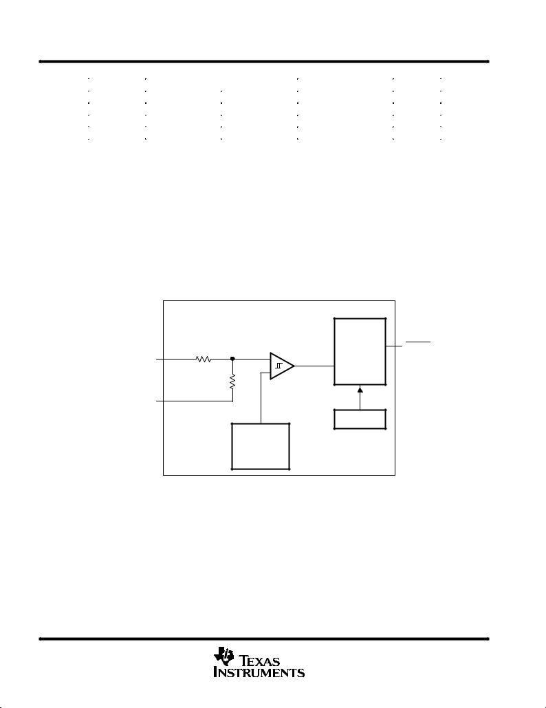
The TPS3809 family of supervisory circuits provides circuit initialization and timing supervision, primarily for DSPs and processor-based systems.
During power-on, RESET is asserted when the supply voltage VDD becomes higher than 1.1 V. Thereafter, the
supervisory circuit monitors VDD and keeps RESET active as long as VDD remains below the threshold voltage VIT. An internal timer delays the return of the output to the inactive state (high) to ensure proper system reset.
The delay time, td(typ) = 200 ms, starts after VDD has risen above the threshold voltage VIT. When the supply voltage drops below the threshold voltage VIT, the output becomes active (low) again. No external components
are required. All the devices of this family have a fixed sense-threshold voltage VIT set by an internal voltage divider.
The product spectrum is designed for supply voltages of 2.5 V, 3 V, 3.3 V, and 5 V. The circuits are available in a 3-pin SOT-23. The TPS3809 devices are characterized for operation over a temperature range of ±40°C to 85°C.
typical applications
|
|
TPS76333 |
|
|
|
3.3 V |
|
5 V |
IN |
OUT |
|
|
|
GND |
VDD |
|
|
VDD |
TMS320LC54x |
|
|
|
|
|
|
TPS3809K33 |
|
|
|
RESET |
RESET |
|
|
GND |
GND |
|
|
|
DApplications Using DSPs, Microcontrollers, or Microprocessors
DWireless Communication Systems
DPortable/Battery-Powered Equipment
DProgrammable Controls
DIntelligent Instruments
DIndustrial Equipment
DNotebook/Desktop Computers
DAutomotive Systems
Please be aware that an important notice concerning availability, standard warranty, and use in critical applications of Texas Instruments semiconductor products and disclaimers thereto appears at the end of this data sheet.
PRODUCTION DATA information is current as of publication date. Products conform to specifications per the terms of Texas Instruments standard warranty. Production processing does not necessarily include testing of all parameters.
Copyright 1999, Texas Instruments Incorporated
POST OFFICE BOX 655303 •DALLAS, TEXAS 75265 |
1 |
TPS3809J25, TPS3809L30, TPS3809K33, TPS3809I50 3-PIN SUPPLY VOLTAGE SUPERVISORS
SLVS228 ± AUGUST 1999
AVAILABLE OPTIONS
TA |
DEVICE NAME |
THRESHOLD VOLTAGE |
MARKING |
||
|
TPS3809J25DBVR² |
TPS3809J25DBVT³ |
2.25 V |
PCZI |
|
±40°C to 85°C |
TPS3809L30DBVR² |
TPS3809L30DBVT³ |
2.64 V |
PDAI |
|
TPS3809K33DBVR² |
TPS3809K33DBVT³ |
2.93 V |
PDBI |
||
|
|||||
|
TPS3809I50DBVR² |
TPS3809I50DBVT³ |
4.55 V |
PDCI |
|
² The DBVR passive indicates tape and reel of 3000 parts. ³ The DBVT passive indicates tape and reel of 250 parts.
FUNCTION/TRUTH TABLE, TPS3809 |
|
|
ORDERING INFORMATION |
||||||||||||||||
|
|
|
|
|
|
TPS380 9 J 25 DBV R |
|||||||||||||
|
VDD>VIT |
|
RESET |
|
|
||||||||||||||
|
|
|
|
|
|
|
|
|
|
|
|
|
|||||||
|
0 |
|
L |
|
|
|
|
|
|
|
|
|
|
|
|
|
Reel |
||
|
1 |
|
H |
|
|
|
|
|
|
|
|
|
|
|
|
|
|||
|
|
|
|
|
|
|
|
|
|
|
|
|
Package |
||||||
|
|
|
|
|
|
|
|
|
|
|
|
|
|
|
|
||||
|
|
|
|
|
|
|
|
|
|
|
|
|
|
Nominal Supply Voltage |
|||||
|
|
|
|
|
|
|
|
|
|
|
|
|
|
||||||
|
|
|
|
|
|
|
|
|
|
|
|
Nominal Threshold Voltage |
|||||||
|
|
|
|
|
|
|
|
|
|
|
|
||||||||
|
|
|
|
|
|
|
|
|
|
Functionality |
|||||||||
|
|
|
|
|
|
|
|
|
|
||||||||||
|
|
|
|
|
|
|
|
Family |
|||||||||||
|
|
|
|
|
|
|
|
||||||||||||
functional block diagram
|
TPS3809 |
|
|
|
|
Reset |
RESET |
R1 |
|
Logic |
|
_ |
|
||
VDD |
+ |
|
|
|
+ |
Timer |
|
|
|
|
|
|
R2 |
|
|
GND |
|
|
|
|
|
Oscillator |
|
|
Reference |
|
|
|
Voltage |
|
|
|
of 1.137 V |
|
|
2 |
POST OFFICE BOX 655303 •DALLAS, TEXAS 75265 |

TPS3809J25, TPS3809L30, TPS3809K33, TPS3809I50 3-PIN SUPPLY VOLTAGE SUPERVISORS
SLVS228 ± AUGUST 1999
timing diagram
VDD
V(NOM)
VIT
1.1 V |
|
|
t |
RESET |
|
1 |
|
0 |
t |
td |
td |
For VDD< 1.1 V Undefined
Behavior of RESET Output
absolute maximum ratings over operating free-air temperature (unless otherwise noted)²
Supply voltage, VDD (see Note1) . . . . . . . . . . . . . . . . . . . . . . . . . . . . . . . . . . . . . . . . . . . . . . . . . . . . . . . . . . . . . . 7 V All other pins (see Note 1) . . . . . . . . . . . . . . . . . . . . . . . . . . . . . . . . . . . . . . . . . . . . . . . . . . . . . . . . . . . ±0.3 V to 7 V
Maximum low output current, IOL . . . . . . . . . . . . . . . . . . . . . . . . . . . . . . . . . . . . . . . . . . . . . . . . . . . . . . . . . . . . 5 mA Maximum high output current, IOH . . . . . . . . . . . . . . . . . . . . . . . . . . . . . . . . . . . . . . . . . . . . . . . . . . . . . . . . . . ±5 mA Input clamp current, IIK (VI<0 or VI>VDD) . . . . . . . . . . . . . . . . . . . . . . . . . . . . . . . . . . . . . . . . . . . . . . . . . . . ±20 mA Output clamp current, IOK (VO<0 or VO>VDD) . . . . . . . . . . . . . . . . . . . . . . . . . . . . . . . . . . . . . . . . . . . . . . . ±20 mA Continuous total power dissipation . . . . . . . . . . . . . . . . . . . . . . . . . . . . . . . . . . . . . . See Dissipation Rating Table
Operating free-air temperature range, TA . . . . . . . . . . . . . . . . . . . . . . . . . . . . . . . . . . . . . . . . . . . . . ±40°C to 85°C Storage temperature range, Tstg . . . . . . . . . . . . . . . . . . . . . . . . . . . . . . . . . . . . . . . . . . . . . . . . . . . . ±65°C to 150°C Soldering temperature . . . . . . . . . . . . . . . . . . . . . . . . . . . . . . . . . . . . . . . . . . . . . . . . . . . . . . . . . . . . . . . . . . . . 260°C
²Stresses beyond those listed under ªabsolute maximum ratingsº may cause permanent damage to the device. These are stress ratings only, and functional operation of the device at these or any other conditions beyond those indicated under ªrecommended operating conditionsº is not
implied. Exposure to absolute±maximum±rated conditions for extended periods may affect device reliability.
NOTE 1: All voltage values are with respect to GND. For reliable operation the device should not be operated at 7 V for more than t=1000h continuously.
DISSIPATION RATING TABLE
PACKAGE |
TA <25°C |
DERATING FACTOR |
TA = 70°C |
TA = 85°C |
|
POWER RATING |
ABOVE TA = 25°C |
POWER RATING |
POWER RATING |
||
|
|||||
DBV |
437 mW |
3.5 mW/°C |
280 mW |
227 mW |
|
|
|
|
|
|
recommended operating conditions at specified temperature range
|
MIN |
MAX |
UNIT |
|
|
|
|
|
|
Supply voltage, VDD |
2 |
6 |
V |
|
Operating free-air temperature range, TA |
±40 |
85 |
°C |
|
|
|
|
|
|
|
|
|
|
|
POST OFFICE BOX 655303 •DALLAS, TEXAS 75265 |
3 |
 Loading...