


Texas Instruments TPS62040DGQ, TPS62040DRC, TPS62042DGQ, TPS62042DRC, TPS62043DGQ Schematic [ru]
...
|
TPS62040 |
|
TPS62042, TPS62043 |
www.ti.com |
TPS62044, TPS62046 |
|
SLVS463B − JUNE 2003 − REVISED OCTOBER 2005 |
1.2 A/1.25 MHz, HIGH-EFFICIENCY STEP-DOWN CONVERTER
FEATURES
DUp to 95% Conversion Efficiency
DTypical Quiescent Current: 18 A
DLoad Current: 1.2 A
DOperating Input Voltage Range: 2.5 V to 6.0 V
DSwitching Frequency: 1.25 MHz
DAdjustable and Fixed Output Voltage
DPower Save Mode Operation at Light load Currents
D100% Duty Cycle for Lowest Dropout
DInternal Softstart
DDynamic Output Voltage Positioning
DThermal Shutdown
DShort-Circuit Protection
D10 Pin MSOP PowerPad™ Package
D10 Pin QFN 3 X 3 mm Package
APPLICATIONS
DPDA, Pocket PC and Smart Phones
DUSB Powered Modems
DCPUs and DSPs
DPC Cards and Notebooks
DxDSL Applications
DStandard 5-V to 3.3-V Conversion
DESCRIPTION
The TPS6204x family of devices are high efficiency synchronous step-down dc-dc converters optimized for battery powered portable applications. The devices are ideal for portable applications powered by a single Li-Ion battery cell or by 3-cell NiMH/NiCd batteries. With an output voltage range from 6.0 V down to 0.7 V, the devices support low voltage DSPs and processors in PDAs, pocket PCs, as well as notebooks and subnotebook computers. The TPS6204x operates at a fixed switching frequency of 1.25 MHz and enters the power save mode operation at light load currents to maintain high efficiency over the entire load current range. For low noise applications, the devices can be forced into fixed frequency PWM mode by pulling the MODE pin high. The TPS6204x supports up to 1.2-A load current.
Typical Application Circuit 1.2-A Output Current
VI |
|
TPS6204x |
|
L1 |
VO |
||
2.5 V to 6 V |
2 |
|
SW |
8 |
6.2 |
H |
0.7 V to VI /1.2 A |
|
VIN |
|
|
|
|||
C1 |
3 |
VIN |
SW |
7 |
|
|
C2 |
1 |
EN |
FB |
5 |
|
|
||
22 F |
|
|
22 F |
||||
|
6 |
MODE |
PGND 10 |
|
|
|
|
|
4 |
GND |
PGND |
9 |
|
|
|
|
|
|
|
|
EFFICIENCY |
|
|
|
|
|
|
|
|
|
|
vs |
|
|
|
|
|
|
|
LOAD CURRENT |
|
|
|||
|
100 |
|
VO = 1.8 V |
|
|
|
|
|
|
|
95 |
|
|
|
|
|
|
||
|
|
|
|
|
|
|
|
|
|
|
90 |
|
VI = 2.7 V |
|
|
|
|
|
|
|
|
|
|
|
|
|
|
|
|
|
85 |
|
VI = 3.6 V |
|
|
|
|
|
|
− % |
80 |
|
VI = 5 V |
|
|
|
|
|
|
75 |
|
|
|
|
|
|
|
|
|
Efficiency |
|
|
|
|
|
|
|
|
|
70 |
|
|
|
|
|
|
|
|
|
65 |
|
|
|
MODE = Low |
|
|
|
||
60 |
|
|
|
|
|
|
|||
|
|
|
|
|
|
|
|
|
|
|
55 |
|
|
|
|
|
|
|
|
|
50 |
|
|
|
|
|
VI = 3.6 V |
|
|
|
45 |
|
|
|
|
|
|
||
|
|
|
|
|
|
MODE = High |
|
||
|
|
|
|
|
|
|
|
||
|
40 |
0 |
0.01 |
0.1 |
1 |
10 |
100 |
1 k |
10 k |
|
|
|
|
IL − Load Current − mA |
|
|
|||
Please be aware that an important notice concerning availability, standard warranty, and use in critical applications of Texas Instruments

 semiconductor products and disclaimers thereto appears at the end of this data sheet. PowerPAD is a trademark of Texas Instruments.
PRODUCTION DATA information is current as of publication date. Products |
Copyright ♥ 2003 − 2005, Texas Instruments Incorporated |
conform to specifications per the terms of Texas Instruments standard warranty. |
|
Production processing does not necessarily include testing of all parameters. |
|

TPS62040 |
|
TPS62042, TPS62043 |
|
TPS62044, TPS62046 |
www.ti.com |
SLVS463B − JUNE 2003 − REVISED OCTOBER 2005 |
|
These devices have limited built-in ESD protection. The leads should be shorted together or the device placed in conductive foam during storage or handling to prevent electrostatic damage to the MOS gates.
ORDERING INFORMATION
|
TA |
VOLTAGE OPTIONS |
PACKAGE |
PACKAGE MARKING |
||
|
|
|
|
|
||
|
MSOP(1) |
QFN(2) |
MSOP |
QFN |
||
|
|
|
||||
|
|
Adjustable |
TPS62040DGQ |
TPS62040DRC |
BBI |
BBO |
|
|
|
|
|
|
|
|
|
1.5 V |
TPS62042DGQ |
TPS62042DRC |
BBL |
BBS |
|
|
|
|
|
|
|
° |
° |
1.6 V |
TPS62043DGQ |
TPS62043DRC |
BBM |
BBT |
−40 C to 85 C |
|
|
|
|
|
|
|
|
1.8 V |
TPS62044DGQ |
TPS62044DRC |
BBN |
BBU |
|
|
|
|
|
|
|
|
|
3.3 V |
TPS62046DGQ |
TPS62046DRC |
BBQ |
BBW |
(1)The DGQ package is available in tape and reel. Add R suffix (DGQR) to order quantities of 2500 parts per reel.
(2)The DRC package is available in tape and reel. Add R suffix (DRCR) to order quantities of 3000 parts per reel.
ABSOLUTE MAXIMUM RATINGS
over operating free-air temperature range unless otherwise noted(1)
|
UNITS |
|
|
Supply voltage VIN (2) |
−0.3 V to 7 V |
Voltages on EN, MODE, FB, SW(2) |
−0.3 V to V +0.3 V |
|
CC |
Continuous power dissipation |
See Dissipation Rating Table |
|
|
Operating junction temperature range |
−40°C to 150°C |
|
|
Storage temperature range |
−65°C to 150°C |
|
|
Lead temperature (soldering, 10 sec) |
260°C |
(1)Stresses beyond those listed under “absolute maximum ratings” may cause permanent damage to the device. These are stress ratings only, and functional operation of the device at these or any other conditions beyond those indicated under recommended operating conditions is not implied.
Exposure to absolute-maximum-rated conditions for extended periods may affect device reliability.
(2)All voltage values are with respect to network ground terminal.
PACKAGE DISSIPATION RATINGS
PACKAGE |
|
RQ (1) |
TA ≤ 25°C |
TA = 70°C |
TA = 85°C |
|
|
JA |
POWER RATING |
POWER RATING |
POWER RATING |
MSOP |
|
60°C/W |
1.67 W |
917 mW |
667 mW |
|
|
|
|
|
|
QFN |
|
48.7°C/W |
2.05 W |
1.13 W |
821 mW |
(1) The thermal resistance, R |
ΘJA |
is based on a soldered PowerPAD using thermal vias. |
|
|
|
|
|
|
|
|
|
RECOMMENDED OPERATING CONDITIONS
|
|
MIN |
TYP MAX |
UNIT |
|
|
|
|
|
VI |
Supply voltage |
2.5 |
6.0 |
V |
VO |
Output voltage range for adjustable output voltage version |
0.7 |
VI |
V |
IO |
Output current |
|
1.2 |
A |
L |
Inductor(1) |
|
6.2 |
H |
C |
Input capacitor(1) |
|
22 |
F |
I |
|
|
|
|
C |
Output capacitor(1) |
|
22 |
F |
O |
|
|
|
|
TA |
Operating ambient temperature |
−40 |
85 |
°C |
TJ |
Operating junction temperature |
−40 |
125 |
°C |
(1) Refer to application section for further information
2

|
|
|
|
|
|
TPS62040 |
|
|
|
|
|
TPS62042, TPS62043 |
|||
www.ti.com |
|
|
TPS62044, TPS62046 |
||||
|
|
|
SLVS463B − JUNE 2003 − REVISED OCTOBER 2005 |
||||
ELECTRICAL CHARACTERISTICS |
|
|
|
|
|
|
|
VI = 3.6 V, VO = 1.8 V, IO = 600 mA, EN = VIN, TA = −40°C to 85°C, typical values are at TA = 25°C (unless otherwise noted)(1) |
|
|
|||||
SUPPLY CURRENT |
|
|
|
|
|
|
|
|
|
|
|
|
|
|
|
|
PARAMETER |
|
TEST CONDITIONS |
MIN |
TYP |
MAX |
UNIT |
|
|
|
|
|
|
|
|
VI |
Input voltage range |
|
|
2.5 |
|
6.0 |
V |
I(Q) |
Operating quiescent current |
|
IO = 0 mA, device is not switching |
|
18 |
35 |
µA |
ISD |
Shutdown supply current |
|
EN = GND |
|
0.1 |
1 |
µA |
VUVLO |
Under−voltage lockout threshold |
|
|
1.5 |
|
2.3 |
V |
ENABLE AND MODE |
|
|
|
|
|
|
|
|
|
|
|
|
|
|
|
VEN |
EN high level input voltage |
|
|
1.4 |
|
|
V |
VEN |
EN low level input voltage |
|
|
|
|
0.4 |
V |
IEN |
EN input bias current |
|
EN = GND or VIN |
|
0.01 |
1.0 |
µA |
V(MODE) |
MODE high level input voltage |
|
|
1.4 |
|
|
V |
V(MODE) |
MODE low level input voltage |
|
|
|
|
0.4 |
V |
I(MODE) |
MODE input bias current |
|
MODE = GND or VIN |
|
0.01 |
1.0 |
µA |
POWER SWITCH |
|
|
|
|
|
|
|
|
|
|
|
|
|
|
|
rDS(ON) |
P-channel MOSFET on−resistance |
|
VI = VGS = 3.6 V |
|
115 |
210 |
mΩ |
P-channel MOSFET on−resistance |
|
VI = VGS = 2.5 V |
|
145 |
270 |
mΩ |
|
|
|
|
|||||
Ilkg(P) |
P-channel leakage current |
|
VDS = 6.0 V |
|
|
1 |
µA |
rDS(ON) |
N-channel MOSFET on−resistance |
|
VI = VGS = 3.6 V |
|
85 |
200 |
mΩ |
N-channel MOSFET on−resistance |
|
VI = VGS = 2.5 V |
|
115 |
280 |
mΩ |
|
|
|
|
|||||
IIkg(N) |
N-channel leakage current |
|
VDS = 6.0 V |
|
|
1 |
µA |
IL |
P-channel current limit |
|
2.5 V < VI< 6.0 V |
1.5 |
1.85 |
2.2 |
A |
|
Thermal shutdown |
|
|
|
150 |
|
°C |
|
|
|
|
|
|
|
|
OSCILLATOR |
|
|
|
|
|
|
|
|
|
|
|
|
|
|
|
fS |
Oscillator frequency |
|
VFB = 0.5 V |
1 |
1.25 |
1.5 |
MHz |
|
VFB = 0 V |
|
625 |
|
kHz |
||
|
|
|
|
|
|||
OUTPUT |
|
|
|
|
|
|
|
|
|
|
|
|
|
|
|
VO |
Adjustable output voltage range |
TPS62040 |
|
0.7 |
|
VIN |
V |
Vref |
Reference voltage |
|
|
|
0.5 |
|
V |
VFB |
Feedback voltage |
TPS62040 |
VI = 2.5 V to 6.0 V; IO= 0 mA |
0% |
|
3% |
|
Adjustable |
VI = 2.5 V to 6.0 V; 0 mA ≤ IO ≤ 1.2 A |
−3% |
|
3% |
|
||
|
|
|
|
||||
|
|
TPS62042 |
VI = 2.5 V to 6.0 V; IO = 0 mA |
0% |
|
3% |
|
|
|
1.5V |
VI = 2.5 V to 6.0 V; 0 mA ≤ IO ≤ 1.2 A |
−3% |
|
3% |
|
|
|
TPS62043 |
VI = 2.5 V to 6.0 V; IO = 0 mA |
0% |
|
3% |
|
VO |
Fixed output voltage |
1.6V |
VI = 2.5 V to 6.0 V; 0 mA ≤ IO ≤ 1.2 A |
−3% |
|
3% |
|
TPS62044 |
VI = 2.5 V to 6.0 V; IO = 0 mA |
0% |
|
3% |
|
||
|
|
|
|
||||
|
|
1.8V |
VI = 2.5 V to 6.0 V; 0 mA ≤ IO ≤ 1.2 A |
−3% |
|
3% |
|
|
|
TPS62046 |
VI = 3.6 V to 6.0 V; IO = 0 mA |
0% |
|
3% |
|
|
|
3.3V |
VI = 3.6 V to 6.0 V; 0 mA ≤ IO ≤ 1.2 A |
−3% |
|
3% |
|
|
Line regulation(1) |
|
VI = VO + 0.5 V (min. 2.5 V) to 6.0 V, |
|
0 |
|
%/V |
|
|
IO = 10 mA |
|
|
|||
|
|
|
|
|
|
|
|
|
Load regulation(1) |
|
I = 10 mA to 1200 mA |
|
0 |
|
%/mA |
|
|
|
O |
|
|
|
|
IIkg(SW) |
Leakage current into SW pin |
|
VI>VO, 0 V ≤ Vsw ≤ VI |
|
0.1 |
1 |
µA |
Reverse leakage current into pin SW |
|
VI = open; EN = GND; VSW = 6.0 V |
|
0.1 |
1 |
µA |
|
|
|
|
|||||
f |
Short circuit switching frequency |
|
VFB = 0 V |
|
625 |
|
kHz |
(1) The line and load regulations are digitally controlled to assure an output voltage accuracy of ±3%.
3
TPS62040 |
|
TPS62042, TPS62043 |
|
TPS62044, TPS62046 |
www.ti.com |
SLVS463B − JUNE 2003 − REVISED OCTOBER 2005 |
|
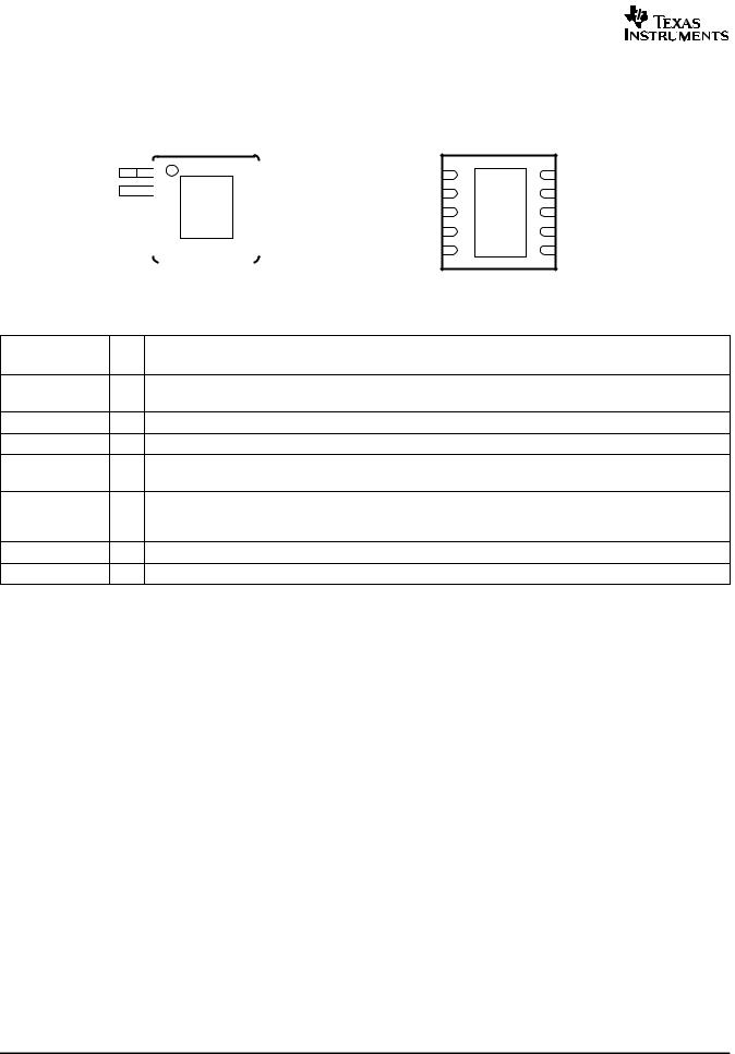
PIN ASSIGNMENTS |
|
DGQ PACKAGE |
DRC PACKAGE |
(TOP VIEW) |
(TOP VIEW) |
EN |
|
1 |
10 |
|
|
|
PGND |
||||
|
|
|
|||||||||
VIN |
|
|
|
2 |
9 |
|
|
|
PGND |
||
|
|
|
|
||||||||
VIN |
|
|
3 |
8 |
|
|
|
SW |
|||
|
|
|
|
|
|
|
|||||
GND |
|
|
4 |
7 |
|
|
|
SW |
|||
|
|
|
|
|
|
|
|||||
FB |
|
|
|
|
5 |
6 |
|
|
|
MODE |
|
|
|
|
|
|
|
|
|||||
NOTE: |
|
|
|
|
|
|
|
||||
|
|
|
|
|
|
|
|
|
|
||
The PowerPAD must be connected to GND. |
|||||||||||
EN |
1 |
10 |
PGND |
VIN |
2 |
9 |
PGND |
VIN |
3 |
8 |
SW |
GND |
4 |
7 |
SW |
FB |
5 |
6 |
MODE |
|
|
|
Terminal Functions |
|
TERMINAL |
I/O |
DESCRIPTION |
||
NAME |
NO. |
|||
|
|
|||
EN |
1 |
I |
Enable. Pulling EN to ground forces the device into shutdown mode. Pulling EN to VI enables the device. EN should |
|
|
|
|
not be left floating and must be terminated. |
|
VIN |
2,3 |
I |
Supply voltage input |
|
GND |
4 |
|
Analog ground |
|
FB |
5 |
I |
Feedback pin. Connect FB directly to the output if the fixed output voltage version is used. For the adjustable version |
|
|
|
|
an external resistor divider is connected to this pin. The internal voltage divider is disabled for the adjustable version. |
|
MODE |
6 |
I |
Pulling the MODE pin high allows the device to be forced into fixed frequency operation. Pulling the MODE pin to low |
|
|
|
|
enables the power save mode where the device operates in fixed frequency PWM mode at high load currents and |
|
|
|
|
in PFM mode (pulse frequency modulation) at light load currents. |
|
SW |
7,8 |
I/O |
This is the switch pin of the converter and is connected to the drain of the internal power MOSFETs |
|
PGND |
9,10 |
|
Power ground |
|
4
www.ti.com
FUNCTIONAL BLOCK DIAGRAM
VIN |
|
VIN |
Undervoltage |
|
Lockout |
|
Bias supply |
EN 

V |
Vcomp |
|
|
|
I |
Soft |
Start |
1.25 MHz
Oscillator
TPS62040 TPS62042, TPS62043 TPS62044, TPS62046
SLVS463B − JUNE 2003 − REVISED OCTOBER 2005
Current limit Comparator
+
− Ref
+ |
Channel−P PowerMOSFET |
|
SkipComparator |
− |
Ref |
MODE |
|
|
Comparator |
S |
|
|
|
|
|
|
|
Driver |
|
|
+ |
|
R |
|
|
|
|
Control Logic |
Shoot−thru |
||
Saw Tooth |
|
|
|
||
− |
|
|
Logic |
||
|
|
|
|||
Generator |
|
|
|
|
|
|
|
Comp High |
|
|
|
|
|
|
|
|
|
|
|
|
Comp Low |
|
|
|
|
|
Comp Low 2 |
|
|
Comp High |
|
|
|
LoadComparator |
|
− |
|
|
|
||
Gm |
Compensation |
|
R1 |
|
+ |
+ |
|
R2 |
|
||
|
|
|
|
||
Comp Low |
|
+ |
|
|
− |
Comp Low 2 |
|
|
|
|
|
|
− |
|
|
|
|
|
Vref = 0.5 V |
|
|
|
|

 SW
SW

 SW
SW
Power MOSFET
N−Channel
|
|
|
|
|
|
|
|
|
|
|
|
|
|
|
|
|
|
|
|
|
|
|
|
|
|
|
|
|
|
MODE |
GND |
FB |
PGND PGND |
|||||||||||
For the Adjustable Version the FB Pin Is
Directly Connected to the Gm Amplifier
5

TPS62040 |
|
|
|
|
TPS62042, TPS62043 |
|
|
|
|
TPS62044, TPS62046 |
|
|
www.ti.com |
|
SLVS463B − JUNE 2003 − REVISED OCTOBER 2005 |
|
|||
|
|
TYPICAL CHARACTERISTICS |
|
|
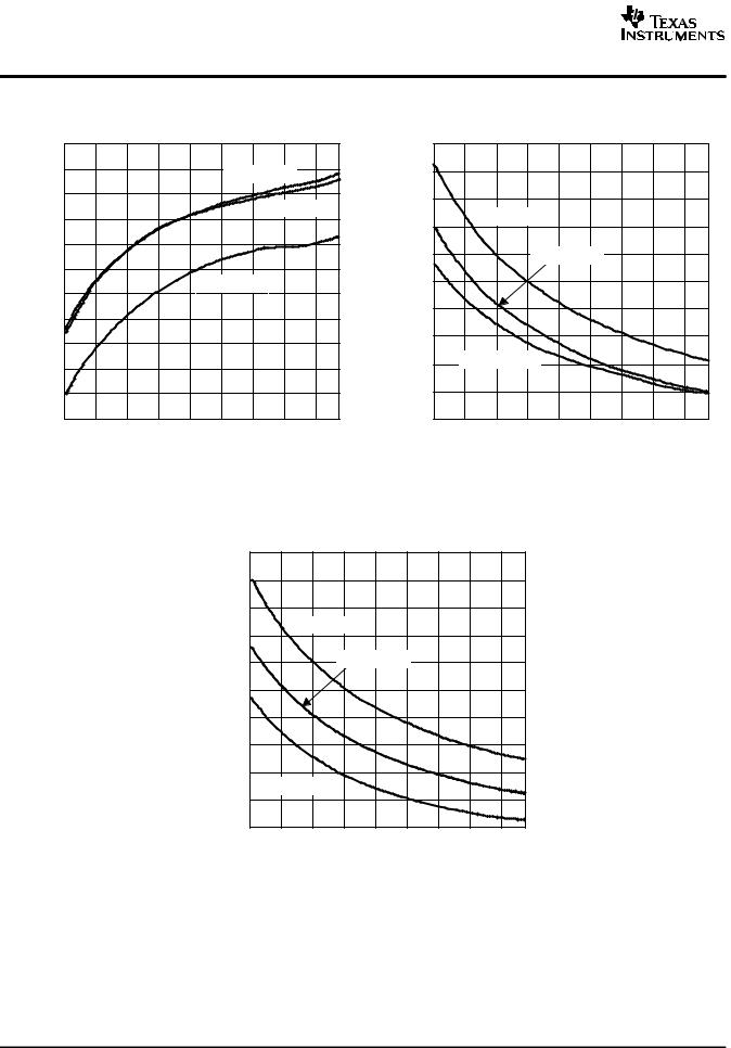
TABLE OF GRAPHS |
|
|
|
|
|
|
|
|
|
|
|
|
|
FIGURE |
|
|
|
|
|
η |
Efficiency |
|
vs Load current |
1, 2, 3 |
η |
Efficiency |
|
vs Input voltage |
4 |
|
|
|
|
|
IQ |
Quiescent current |
|
vs Input voltage |
5, 6 |
fs |
Switching frequency |
|
vs Input voltage |
7 |
rDS(on) |
P-Channel rDS(on) |
|
vs Input voltage |
8 |
rDS(on) |
N-Channel rectifier rDS(on) |
|
vs Input voltage |
9 |
|
Load transient response |
|
|
10 |
|
|
|
|
|
|
PWM operation |
|
|
11 |
|
|
|
|
|
|
Power save mode |
|
|
12 |
|
|
|
|
|
|
Start-up |
|
|
13 |
|
|
|
|
|
|
|
|
|
|
EFFICIENCY |
|
|
|
|
|
|
|
|
|
|
|
vs |
|
|
|
|
|
|
|
|
LOAD CURRENT |
|
|
|
|||
|
100 |
|
VO = 3.3 V |
|
|
|
|
|
|
|
|
95 |
|
|
|
|
|
|
|
|
|
|
|
|
|
|
|
|
|
|
|
|
|
90 |
|
VI = 3.6 V |
|
|
|
|
|
|
|
|
85 |
|
MODE = Low |
|
|
|
|
|
|
|
|
|
|
|
|
|
|
|
|
|
|
|
80 |
|
|
|
|
|
VI = 5 V |
|
|
|
− % |
|
|
|
|
|
MODE = Low |
− % |
|||
|
|
|
|
|
|
|||||
75 |
|
|
|
|
|
|
|
|
||
Efficiency |
70 |
|
|
|
|
|
VI = 3.6 V |
|
Efficiency |
|
65 |
|
|
|
|
|
MODE = High |
||||
|
|
|
|
|
|
|
|
|||
|
|
|
|
|
|
|
|
|
||
|
60 |
|
|
|
|
|
VI = 5 V |
|
|
|
|
55 |
|
|
|
|
|
MODE = High |
|
||
|
|
|
|
|
|
|
|
|
|
|
|
50 |
|
|
|
|
|
|
|
|
|
|
45 |
|
|
|
|
|
|
|
|
|
|
40 |
0 |
0.01 |
0.1 |
1 |
10 |
100 |
1 k |
10 k |
|
|
|
|
|
IL − Load Current − mA |
|
|
|
|||
Figure 1
|
|
|
|
EFFICIENCY |
|
|
|
|
|
|
|
|
|
vs |
|
|
|
|
|
|
|
LOAD CURRENT |
|
|
||
100 |
|
VO = 1.8 V |
|
|
|
|
|
|
95 |
|
|
|
|
|
|
||
|
VI = 2.7 V |
|
|
|
|
|
||
90 |
|
|
|
|
|
|
||
|
|
|
|
|
|
|
|
|
85 |
|
VI = 3.6 V |
|
|
|
|
|
|
|
|
|
|
|
|
|
|
|
80 |
|
VI = 5 V |
|
|
|
|
|
|
75 |
|
|
|
|
|
|
|
|
70 |
|
|
|
MODE = Low |
|
|
|
|
65 |
|
|
|
|
|
|
||
|
|
|
|
|
VI = 3.6 V |
|
||
60 |
|
|
|
|
|
|
||
|
|
|
|
|
MODE = High |
|
||
|
|
|
|
|
|
|
||
55 |
|
|
|
|
|
|
|
|
50 |
|
|
|
|
|
|
|
|
45 |
|
|
|
|
|
|
|
|
40 |
0 |
0.01 |
0.1 |
1 |
10 |
100 |
1 k |
10 k |
|
|
|
IL − Load Current − mA |
|
|
|||
Figure 2
6

|
|
|
|
|
|
|
|
|
|
|
|
|
|
|
|
|
TPS62040 |
|
|
|
|
|
|
|
|
|
|
|
|
|
|
|
|
TPS62042, TPS62043 |
|||
|
www.ti.com |
|
|
|
|
|
|
|
|
|
|
|
TPS62044, TPS62046 |
|||||
|
|
|
|
|
|
|
|
|
|
|
|
|
SLVS463B − JUNE 2003 − REVISED OCTOBER 2005 |
|||||
|
|
|
|
|
EFFICIENCY |
|
|
|
|
|
|
|
EFFICIENCY |
|
|
|
||
|
|
|
|
|
|
vs |
|
|
|
|
|
|
|
|
vs |
|
|
|
|
|
|
|
|
LOAD CURRENT |
|
|
|
|
|
INPUT VOLTAGE |
|
|
|
||||
|
100 |
|
VO = 1.5 V |
|
|
|
|
|
|
100 |
VO = 1.8 V |
|
|
|
|
|
||
|
95 |
|
|
|
|
|
|
|
|
|
|
|
|
|
||||
|
|
|
|
|
|
|
|
|
|
|
MODE = Low |
|
|
|
|
|
||
|
|
|
|
|
|
|
|
|
|
|
|
|
|
|
|
|
||
|
90 |
|
VI = 2.7 V |
|
|
|
|
|
95 |
|
|
|
|
|
|
|
||
|
85 |
|
VI = 3.6 V |
|
|
|
|
|
|
|
|
|
|
|
IL = 500 mA |
|
|
|
|
80 |
|
|
|
|
|
|
|
|
90 |
|
|
|
|
|
|
|
|
− % |
|
|
|
|
|
|
|
|
− % |
|
|
|
|
|
|
|
||
75 |
|
VI = 5 V |
|
|
|
|
|
|
|
|
|
|
|
|
|
|
||
Efficiency |
70 |
|
|
|
|
|
|
|
|
Efficiency |
85 |
IL = 1000 mA |
|
|
|
|
|
|
65 |
|
|
|
|
|
|
|
|
|
|
|
|
IL = 1 mA |
|
|
|||
|
|
|
|
|
|
|
|
|
|
|
|
|
|
|
|
|
||
|
60 |
|
|
|
|
|
|
|
|
|
80 |
|
|
|
|
|
|
|
|
55 |
|
|
|
|
|
|
|
|
|
|
|
|
|
|
|
|
|
|
50 |
|
|
|
|
|
|
|
|
|
75 |
|
|
|
|
|
|
|
|
45 |
|
|
|
|
|
|
|
|
|
|
|
|
|
|
|
|
|
|
40 |
0 |
0.01 |
0.1 |
1 |
10 |
100 |
1 k |
10 k |
|
70 |
|
|
|
|
|
|
|
|
|
2.5 |
3 |
3.5 |
4 |
4.5 |
5 |
5.5 |
6 |
|||||||||
|
|
|
|
IL − Load Current − mA |
|
|
|
|
|
VI − Input Voltage − V |
|
|
|
|||||
|
|
|
|
|
Figure 3 |
|
|
|
|
|
|
|
Figure 4 |
|
|
|
||
|
|
|
|
QUIESCENT CURRENT |
|
|
|
|
|
QUIESCENT CURRENT |
|
|
||||||
|
|
|
|
|
|
vs |
|
|
|
|
|
|
|
|
vs |
|
|
|
|
|
|
|
|
INPUT VOLTAGE |
|
|
|
|
|
|
INPUT VOLTAGE |
|
|
||||
|
23 |
|
|
|
|
|
|
|
|
|
7.5 |
|
|
|
|
|
|
|
MODE = Low |
MODE = High |
|
21 |
|
|
|
TA = 85°C |
|
|
|
|
|
7 |
|
|
|
|
|
|
|
|
A |
19 |
|
|
|
TA = 25°C |
|
|
|
|
mA |
6.5 |
|
|
|
TA = 25°C |
|
|
|
|
|
|
|
|
|
|
|
|
|
|
|
|
|
|
|
|||||
− |
17 |
|
|
|
|
|
|
|
|
|
− |
6 |
|
|
|
|
|
|
|
Current |
|
|
|
|
|
|
|
|
|
Current |
|
|
|
|
|
|
|
||
15 |
|
|
|
TA = −40°C |
|
|
|
5.5 |
|
|
|
|
|
|
|
||||
|
|
|
|
|
|
|
|
|
|
|
|
|
|
|
|
||||
|
|
|
|
|
|
|
|
|
|
|
|
|
|
|
|
|
|
||
Quisecent |
13 |
|
|
|
|
|
|
|
|
|
Quisecent |
5 |
|
|
|
|
|
|
|
11 |
|
|
|
|
|
|
|
|
|
4.5 |
|
|
|
|
|
|
|
||
|
|
|
|
|
|
|
|
|
|
|
|
|
|
|
|
|
|
||
|
9 |
|
|
|
|
|
|
|
|
|
|
4 |
|
|
|
|
|
|
|
|
7 |
|
|
|
|
|
|
|
|
|
|
3.5 |
|
|
|
|
|
|
|
|
5 |
|
|
|
|
|
|
|
|
|
|
3 |
|
|
|
|
|
|
|
|
2.4 |
2.8 |
3.2 |
3.6 |
4 |
4.4 |
4.8 |
5.2 |
5.6 |
6 |
|
2.5 |
3 |
3.5 |
4 |
4.5 |
5 |
5.5 |
6 |
|
|
|
|
VI − Input Voltage − V |
|
|
|
|
|
|
VI − Input Voltage − V |
|
|
||||||
|
|
|
|
Figure 5 |
|
|
|
|
|
|
|
|
Figure 6 |
|
|
|
|||
7
TPS62040 |
|
|
|
|
|
|
|
|
|
|
|
|
|
|
|
|
|
|
|
|
|
TPS62042, TPS62043 |
|
|
|
|
|
|
|
|
|
|
|
|
|
|
|
|
|
||||
TPS62044, TPS62046 |
|
|
|
|
|
|
|
|
|
|
|
|
|
|
www.ti.com |
|
|||||
SLVS463B − JUNE 2003 − REVISED OCTOBER 2005 |
|
|
|
|
|
|
|
|
|
|
|
|
|
|
|||||||
|
|
|
SWITCHING FREQUENCY |
|
|
|
|
|
|
P-CHANNEL rDS(on) |
|
|
|
||||||||
|
|
|
|
|
vs |
|
|
|
|
|
|
|
|
|
|
vs |
|
|
|
|
|
|
|
|
|
INPUT VOLTAGE |
|
|
|
|
|
|
|
INPUT VOLTAGE |
|
|
|
||||||
|
1.23 |
|
|
|
|
|
|
|
|
|
|
0.180 |
|
|
|
|
|
|
|
|
|
|
1.23 |
|
|
|
|
|
TA = 85°C |
|
|
|
0.170 |
|
|
|
|
|
|
|
|
|
|
MHz |
1.22 |
|
|
|
|
|
|
TA = 25°C |
|
−Ω |
0.160 |
|
|
|
|
|
|
|
|
|
|
|
|
|
|
|
|
|
|
|
|
|
|
|
|
|
|
|
|||||
1.22 |
|
|
|
|
|
|
|
|
|
TA = 85°C |
|
|
|
|
|
|
|||||
|
|
|
|
|
|
|
|
|
0.150 |
|
|
|
|
|
|
|
|||||
− |
|
|
|
|
|
|
|
|
|
|
DS(on) |
|
|
|
|
|
|
|
|
|
|
1.21 |
|
|
|
|
|
|
|
|
|
0.140 |
|
|
|
TA = 25°C |
|
|
|
|
|||
|
|
|
|
|
|
|
|
|
|
|
|
|
|
|
|
|
|||||
SwitchingFrequency |
1.21 |
|
|
|
|
|
° |
|
|
|
P−Channel r |
0.130 |
|
|
|
|
|
|
|
|
|
|
|
|
|
|
|
|
|
|
|
|
|
|
|
|
|
|
|
||||
1.20 |
|
|
|
TA = −40 C |
|
|
|
|
|
|
|
|
|
|
|
|
|
||||
|
|
|
|
|
|
|
|
|
|
|
|
|
|
|
|
|
|
|
|||
1.20 |
|
|
|
|
|
|
|
|
|
0.120 |
|
|
|
|
|
|
|
|
|
||
|
|
|
|
|
|
|
|
|
|
|
|
|
|
|
|
|
|
|
|||
1.19 |
|
|
|
|
|
|
|
|
|
0.110 |
|
|
|
|
|
|
|
|
|
||
|
|
|
|
|
|
|
|
|
|
|
|
|
|
|
|
|
|
|
|||
f − |
|
|
|
|
|
|
|
|
|
|
|
|
TA = −40°C |
|
|
|
|
|
|
||
1.19 |
|
|
|
|
|
|
|
|
|
|
0.100 |
|
|
|
|
|
|
|
|||
|
|
|
|
|
|
|
|
|
|
|
|
|
|
|
|
|
|
|
|
|
|
|
1.18 |
|
|
|
|
|
|
|
|
|
|
0.090 |
|
|
|
|
|
|
|
|
|
|
|
|
|
|
|
|
|
|
|
|
|
|
|
|
|
|
|
|
|
|
|
|
1.18 |
|
|
|
|
|
|
|
|
|
|
0.080 |
|
|
|
|
|
|
|
|
|
|
2.5 |
2.9 |
3.3 |
3.7 |
4.1 |
4.5 |
4.9 |
5.3 |
5.7 |
6 |
|
2.5 |
2.9 |
3.3 |
3.7 |
4.1 |
4.5 |
4.9 |
5.3 |
5.7 |
6 |
|
|
|
|
VI − Input Voltage − V |
|
|
|
|
|
|
|
VI − Input Voltage − V |
|
|
|
||||||
|
|
|
|
Figure 7 |
|
|
|
|
|
|
|
|
|
Figure 8 |
|
|
|
|
|
||
N-CHANNEL RECTIFIER rDS(on) vs
INPUT VOLTAGE
|
0.150 |
|
|
|
|
|
|
|
|
|
|
0.140 |
|
|
|
|
|
|
|
|
|
Ω |
0.130 |
|
|
|
|
|
|
|
|
|
− |
|
|
|
|
|
|
|
|
|
|
DS(on) |
0.120 |
|
TA = 85°C |
|
|
|
|
|
|
|
|
|
|
|
|
|
|
|
|
||
0.110 |
|
|
TA = 25°C |
|
|
|
|
|
||
r |
|
|
|
|
|
|
|
|||
Rectifier |
0.100 |
|
|
|
|
|
|
|
|
|
0.090 |
|
|
|
|
|
|
|
|
|
|
N-Channel |
|
|
|
|
|
|
|
|
|
|
0.080 |
|
|
|
|
|
|
|
|
|
|
0.070 |
|
|
|
|
|
|
|
|
|
|
|
TA = −40°C |
|
|
|
|
|
|
|
||
|
|
|
|
|
|
|
|
|
||
|
0.060 |
|
|
|
|
|
|
|
|
|
|
0.050 |
|
|
|
|
|
|
|
|
|
|
2.5 |
2.9 |
3.3 |
3.7 |
4.1 |
4.5 |
4.9 |
5.3 |
5.7 |
6 |
|
|
|
|
VI − Input Voltage − V |
|
|
|
|||
Figure 9
8
www.ti.com
LOAD TRANSIENT RESPONSE
VI = 3.6 V
VO = 1.8 V
PWM/PFM Operation
V |
100mV/div |
O |
|
O to 1.15 A |
|
I |
150mA |
50 s/div
Figure 10
POWER SAVE MODE
V |
V/div5 |
SW |
|
V |
mV/div |
O |
|
|
20 |
I |
mA/div |
L |
|
|
500 |
2.5 s/div
Figure 12
V |
V/div5 |
SW |
|
V |
mV/div |
O |
|
|
20 |
I |
mA/div |
L |
|
|
500 |
Enable |
2 V/div |
V |
V/div1 |
O |
|
I |
mA/div |
IN |
|
|
200 |
TPS62040 TPS62042, TPS62043 TPS62044, TPS62046
SLVS463B − JUNE 2003 − REVISED OCTOBER 2005
PWM OPERATION
500 ns/div
Figure 11
START-UP
VI = 3.6 V
VO = 1.8 V
IO = 1.1 A
200 s/div
Figure 13
9
 Loading...