


Texas Instruments TPA711EVM, TPA711MSOPEVM, TPA711DR, TPA711DGNR, TPA711DGN Datasheet
...TPA711 700-mW MONO LOW-VOLTAGE AUDIO POWER AMPLIFIER
|
|
SLOS230B ± NOVEMBER 1998 ± REVISED MARCH 2000 |
|||||||||||
|
|
|
|
|
|
|
|
|
|
|
|
|
|
D Fully Specified for 3.3-V and 5-V Operation |
D BTL to SE Mode Control |
|
|
|
|
|
|
||||||
D Wide Power Supply Compatibility |
D Integrated Depop Circuitry |
|
|||||||||||
|
2.5 V ± 5.5 V |
D Thermal and Short-Circuit Protection |
|||||||||||
D |
Output Power |
D Surface-Mount Packaging |
|
||||||||||
|
± 700 mW at VDD = 5 V, BTL, RL = 8 Ω |
|
|||||||||||
|
± SOIC |
|
|
|
|
|
|
|
|||||
|
± 85 mW at VDD = 5 V, SE, RL = 32 Ω |
± PowerPAD MSOP |
|
|
|
|
|
|
|||||
|
± 250 mW at VDD = 3.3 V, BTL, RL = 8 Ω |
|
|
|
|
|
|
|
|
|
|
|
|
|
± 37 mW at VDD = 3.3 V, SE, RL = 32 Ω |
|
D OR DGN PACKAGE |
|
|||||||||
D |
Shutdown Control |
|
|
|
|
|
(TOP VIEW) |
|
|||||
|
± IDD = 7 µA at 3.3 V |
SHUTDOWN |
|
|
|
|
|
|
|
|
VO± |
||
|
|
|
1 |
8 |
|
|
|
|
|||||
|
± IDD = 50 µA at 5 V |
|
|
|
|
|
|
||||||
|
|
|
|
|
|
||||||||
|
BYPASS |
|
|
2 |
7 |
|
|
|
|
GND |
|||
|
|
|
|
|
|
|
|
|
|
|
|
|
|
description |
SE/BTL |
|
|
|
3 |
6 |
|
|
|
|
VDD |
||
|
|
|
|
|
|
|
|||||||
|
|
|
IN |
|
|
4 |
5 |
|
|
|
|
VO+ |
|
|
|
|
|
|
|
|
|
|
|||||
The TPA711 is a bridge-tied load (BTL) or single-ended (SE) audio power amplifier devel-
oped especially for low-voltage applicationswhere internal speakers and external earphone operation are required. Operating with a 3.3-V supply, the TPA711 can deliver 250-mW of continuous power into a BTL 8-Ω load at less than 0.6% THD+N throughout voice band frequencies. Although this device is characterized out to 20 kHz, its operation was optimized for narrower band applications such as wireless communications. The BTL configuration eliminates the need for external coupling capacitors on the output in most applications, which is particularly important for small battery-powered equipment. A unique feature of the TPA711 is that it allows the amplifier to switch from BTL to SE on the fly when an earphone drive is required. This eliminates complicated mechanical switching or auxiliary devices just to drive the external load. This device features a shutdown mode for power-sensitive applications with special depop circuitry to eliminate speaker noise when exiting shutdown mode. The TPA711 is available in an 8-pin SOIC and the surface-mount PowerPAD MSOP package, which reduces board space by 50% and height by 40%.
RF |
|
|
|
VDD |
6 |
VDD |
|
|
|
|
|
||
Audio |
|
|
VDD/2 |
|
|
CS |
Input |
|
|
|
|
|
|
RI |
4 |
IN |
± |
VO+ |
5 |
|
|
|
|
|
|||
CI |
2 |
BYPASS |
+ |
|
|
|
|
|
|
|
|||
|
|
|
|
|
||
CB |
|
|
|
|
|
|
|
|
|
± |
VO± |
8 |
700 mW |
|
|
|
+ |
|
7 |
|
|
|
|
|
|
|
|
From System Control |
1 |
SHUTDOWN |
Bias |
GND |
|
|
|
|
|
|
|
||
|
3 |
SE/BTL |
|
|
|
|
From HP Jack |
Control |
|
|
|
||
|
|
|
|
|
|
Please be aware that an important notice concerning availability, standard warranty, and use in critical applications of Texas Instruments semiconductor products and disclaimers thereto appears at the end of this data sheet.
PowerPAD is a trademark of Texas Instruments.
PRODUCTION DATA information is current as of publication date. Products conform to specifications per the terms of Texas Instruments standard warranty. Production processing does not necessarily include testing of all parameters.
Copyright 2000, Texas Instruments Incorporated
POST OFFICE BOX 655303 •DALLAS, TEXAS 75265 |
1 |

TPA711
700-mW MONO LOW-VOLTAGE AUDIO POWER AMPLIFIER
SLOS230B ± NOVEMBER 1998 ± REVISED MARCH 2000
AVAILABLE OPTIONS
|
PACKAGED DEVICES |
MSOP |
||
|
|
|
||
TA |
SMALL OUTLINE² |
MSOP³ |
||
SYMBOLIZATION |
||||
|
(D) |
(DGN) |
|
|
|
|
|
|
|
± 40°C to 85°C |
TPA711D |
TPA711DGN |
ABB |
|
|
|
|
|
|
² In the SOIC package, the maximum RMS output power is thermally limited to 350 mW; 700 mW peaks can be driven, as long as the RMS value is less than 350 mW.
³The D and DGN packages are available taped and reeled. To order a taped and reeled part, add the suffix R to the part number (e.g., TPA311DR).
|
|
|
|
|
|
|
Terminal Functions |
|||
|
|
|
|
|
|
|
|
|
|
|
|
TERMINAL |
|
I/O |
|
|
DESCRIPTION |
||||
|
NAME |
NO. |
|
|
||||||
|
|
|
|
|
|
|
||||
|
|
|
|
|
|
|
|
|
|
|
BYPASS |
2 |
I |
BYPASS is the tap to the voltage divider for internal mid-supply bias. This terminal should be connected to |
|||||||
a 0.1- F to 2.2- F capacitor when used as an audio amplifier. |
||||||||||
|
|
|
|
|
||||||
|
|
|
|
|
|
|
|
|
|
|
GND |
7 |
|
GND is the ground connection. |
|||||||
|
|
|
|
|
|
|
|
|
|
|
IN |
4 |
I |
IN is the audio input terminal. |
|||||||
|
|
|
|
|
|
|
|
|||
|
|
|
3 |
I |
|
|
|
|
|
|
SE/BTL |
|
When SE/BTL is held low, the TPA711 is in BTL mode. When SE/BTL is held high, the TPA711 is in SE mode. |
||||||||
|
|
|
|
|||||||
SHUTDOWN |
1 |
I |
SHUTDOWN places the entire device in shutdown mode when held high (IDD = 7 A). |
|||||||
VDD |
6 |
|
VDD is the supply voltage terminal. |
|||||||
VO+ |
5 |
O |
VO+ is the positive output for BTL and SE modes. |
|||||||
VO± |
8 |
O |
VO± is the negative output in BTL mode and a high-impedance output in SE mode. |
|||||||
absolute maximum ratings over operating free-air temperature range (unless otherwise noted)§
Supply voltage, VDD . . . . . . . . . . . . . . . . . . . . . . . . . . . . . . . . . . |
. . . . . . . . . . . . . . . . . . . . . . . |
. . . . . . . . . . . . . . . 6 |
V |
Input voltage, VI . . . . . . . . . . . . . . . . . . . . . . . . . . . . . . . . . . . . . . |
. . . . . . . . . . . . . . . . . . . . . . |
±0.3 V to VDD +0.3 |
V |
Continuous total power dissipation . . . . . . . . . . . . . . . . . . . . . |
internally limited (see Dissipation Rating Table) |
||
Operating free-air temperature range, TA (see Table 3) . . . . |
. . . . . . . . . . . . . . . . . . . . . . . |
. . . . . ±40°C to 85°C |
|
Operating junction temperature range, TJ . . . . . . . . . . . . . . . . |
. . . . . . . . . . . . . . . . . . . . . . . |
. . . . ±40°C to 150°C |
|
Storage temperature range, Tstg . . . . . . . . . . . . . . . . . . . . . . . . |
. . . . . . . . . . . . . . . . . . . . . . . |
. . . . ±65°C to 150°C |
|
Lead temperature 1,6 mm (1/16 inch) from case for 10 seconds . . . . . . . . . . . . . . . . . . . |
. . . . . . . . . . . . 260°C |
||
§Stresses beyond those listed under ªabsolute maximum ratingsº may cause permanent damage to the device. These are stress ratings only, and functional operation of the device at these or any other conditions beyond those indicated under ªrecommended operating conditionsº is not implied. Exposure to absolute-maximum-rated conditions for extended periods may affect device reliability.
DISSIPATION RATING TABLE
PACKAGE |
TA ≤ 25°C |
DERATING FACTOR |
TA = 70°C |
TA = 85°C |
D |
725 mW |
5.8 mW/°C |
464 mW |
377 mW |
|
|
|
|
|
DGN |
2.14 W¶ |
17.1 mW/°C |
1.37 W |
1.11 W |
¶Please see the Texas Instruments document, PowerPAD Thermally Enhanced Package Application Report
(literature number SLMA002), for more information on the PowerPAD package. The thermal data was measured on a PCB layout based on the information in the section entitled Texas Instruments Recommended Board for PowerPAD on page 33 of the before mentioned document.
recommended operating conditions
|
MIN |
|
MAX |
UNIT |
|
|
|
|
|
|
|
Supply voltage, VDD |
2.5 |
|
5.5 |
V |
|
Operating free-air temperature, TA (see Table 3) |
± 40 |
|
85 |
°C |
|
|
|
|
|
|
|
|
|
|
|
|
|
2 |
POST OFFICE BOX 655303 •DALLAS, TEXAS 75265 |
TPA711 700-mW MONO LOW-VOLTAGE AUDIO POWER AMPLIFIER
SLOS230B ± NOVEMBER 1998 ± REVISED MARCH 2000
electrical characteristics at specified free-air temperature, VDD = 3.3 V, TA = 25°C (unless otherwise noted)
|
PARAMETER |
TEST CONDITIONS |
MIN TYP |
MAX |
UNIT |
||||
|
|
|
|
|
|
|
|
|
|
VOO |
Output offset voltage (measured differentially) |
See Note 1 |
|
|
|
20 |
|
mV |
|
PSRR |
Power supply rejection ratio |
VDD = 3.2 V to 3.4 V |
BTL mode |
|
|
85 |
|
|
dB |
|
|
|
|
|
|
||||
SE mode |
|
|
83 |
|
|
||||
|
|
|
|
|
|
|
|
||
|
|
|
|
|
|
|
|
|
|
IDD |
Supply current (see Figure 6) |
BTL mode |
|
|
1.25 |
2.5 |
|
mA |
|
|
|
|
|
|
|
|
|||
SE mode |
|
|
0.65 |
1.25 |
|
||||
|
|
|
|
|
|
||||
|
|
|
|
|
|
|
|
|
|
IDD(SD) |
Supply current, shutdown mode (see Figure 7) |
|
|
|
|
7 |
50 |
|
µA |
NOTE 1: At 3 V < VDD < 5 V the dc output voltage is approximately VDD/2.
operating characteristics, VDD = 3.3 V, TA = 25°C, RL = 8 Ω
|
PARAMETER |
|
TEST CONDITIONS |
|
MIN |
TYP |
MAX |
UNIT |
|
|
|
|
|
|
|
|
|
|
|
|
|
THD = 0.2%, |
BTL mode, |
See Figure 14 |
|
250 |
|
|
|
PO |
Output power, see Note 2 |
|
|
|
|
|
|
mW |
|
THD = 0.1%, |
SE mode, |
RL = 32 Ω, |
|
37 |
|
|
|||
|
|
See Figure 22 |
|
|
|
|
|
|
|
|
|
|
|
|
|
|
|
|
|
|
|
|
|
|
|
|
|
|
|
THD + N |
Total harmonic distortion plus noise |
PO = 250 mW, |
f = 200 Hz to 4 kHz, |
See Figure 12 |
|
0.55% |
|
|
|
BOM |
Maximum output power bandwidth |
Gain = 2, |
THD = 2%, |
See Figure 12 |
|
20 |
|
kHz |
|
B1 |
Unity-gain bandwidth |
Open Loop, |
See Figure 36 |
|
|
1.4 |
|
MHz |
|
|
|
f = 1 kHz, |
CB = 1 µF, |
BTL mode, |
|
79 |
|
|
|
|
|
See Figure 5 |
|
|
|
|
|
|
|
|
Supply ripple rejection ratio |
|
|
|
|
|
dB |
|
|
|
|
|
|
|
|
|
|
||
|
f = 1 kHz, |
CB = 1 µF, |
SE mode, |
|
70 |
|
|
||
|
|
|
|
|
|
||||
|
|
See Figure 3 |
|
|
|
|
|
|
|
|
|
|
|
|
|
|
|
|
|
|
|
|
|
|
|
|
|
|
|
Vn |
Noise output voltage |
Gain = 1, |
CB = 0.1 µF, |
See Figure 42 |
|
17 |
|
µV(rms) |
|
NOTE 2: Output power is measured at the output terminals of the device at f = 1 kHz. |
|
|
|
|
|
|
|||
POST OFFICE BOX 655303 •DALLAS, TEXAS 75265 |
3 |
TPA711
700-mW MONO LOW-VOLTAGE AUDIO POWER AMPLIFIER
SLOS230B ± NOVEMBER 1998 ± REVISED MARCH 2000
electrical characteristics at specified free-air temperature, VDD = 5 V, TA = 25°C (unless otherwise noted)
|
PARAMETER |
TEST CONDITIONS |
MIN TYP |
MAX |
UNIT |
||||
|
|
|
|
|
|
|
|
|
|
VOO |
Output offset voltage (measured differentially) |
|
|
|
|
|
20 |
|
mV |
PSRR |
Power supply rejection ratio |
VDD = 4.9 V to 5.1 V |
BTL mode |
|
|
78 |
|
|
dB |
|
|
|
|
|
|
||||
SE mode |
|
|
76 |
|
|
||||
|
|
|
|
|
|
|
|
||
|
|
|
|
|
|
|
|
|
|
IDD |
Supply current (see Figure 6) |
BTL mode |
|
|
1.25 |
2.5 |
|
mA |
|
|
|
|
|
|
|
|
|||
SE mode |
|
|
0.65 |
1.25 |
|
||||
|
|
|
|
|
|
||||
|
|
|
|
|
|
|
|
|
|
IDD(SD) |
Supply current, shutdown mode (see Figure 7) |
|
|
|
|
50 |
100 |
|
µA |
operating characteristics, VDD = 5 V, TA = 25°C, RL = 8 Ω
|
PARAMETER |
|
TEST CONDITIONS |
|
MIN |
TYP |
MAX |
UNIT |
|
|
|
|
|
|
|
|
|
|
|
|
|
|
THD = 0.3%, |
BTL mode, |
See Figure 18 |
|
700² |
|
|
PO |
Output power, see Note 2 |
|
THD = 0.1%, |
SE mode, |
RL = 32 Ω, |
|
85 |
|
mW |
|
|
|
See Figure 26 |
|
|
|
|
|
|
|
|
|
|
|
|
|
|
|
|
|
|
|
|
|
|
|
|
|
|
THD + N |
Total harmonic distortion plus |
|
PO = 700 mW, |
f = 200 Hz to 4 kHz, |
See Figure 16 |
|
0.5% |
|
|
noise |
|
|
|
|
|||||
|
|
|
|
|
|
|
|
|
|
|
|
|
|
|
|
|
|
|
|
BOM |
Maximum output power bandwidth |
|
Gain = 2, |
THD = 2%, |
See Figure 16 |
|
20 |
|
kHz |
B1 |
Unity-gain bandwidth |
|
Open Loop, |
See Figure 37 |
|
|
1.4 |
|
MHz |
|
|
|
f = 1 kHz, |
CB = 1 µF, |
BTL mode, |
|
80 |
|
|
|
|
|
See Figure 5 |
|
|
|
|
|
|
|
Supply ripple rejection ratio |
|
|
|
|
|
|
dB |
|
|
|
|
|
|
|
|
|
||
|
|
f = 1 kHz, |
CB = 1 µF, |
SE mode, |
|
73 |
|
||
|
|
|
|
|
|
||||
|
|
|
See Figure 4 |
|
|
|
|
|
|
|
|
|
|
|
|
|
|
|
|
|
|
|
|
|
|
|
|
|
|
Vn |
Noise output voltage |
|
Gain = 1, |
CB = 0.1 µF, |
See Figure 43 |
|
17 |
|
µV(rms) |
²The DGN package, properly mounted, can conduct 700 mW RMS power continuously. The D package, can only conduct 350 mW RMS power continuously, with peaks to 700 mW.
NOTE 2: Output power is measured at the output terminals of the device at f = 1 kHz.
4 |
POST OFFICE BOX 655303 •DALLAS, TEXAS 75265 |
|
|
|
|
|
|
TPA711 |
|
|
|
700-mW MONO LOW-VOLTAGE AUDIO POWER AMPLIFIER |
|||
|
|
|
|
|
SLOS230B ± NOVEMBER 1998 ± REVISED MARCH 2000 |
|
|
PARAMETER MEASUREMENT INFORMATION |
|||||
|
|
|
|
|
VDD |
6 |
|
RF |
|
|
|
|
VDD |
Audio |
|
V |
/2 |
|
CS |
|
|
|
|
||||
|
|
DD |
|
|
|
|
Input |
|
|
|
|
|
|
RI |
4 |
IN |
|
± |
VO+ |
5 |
|
|
|
|
|||
CI |
2 |
BYPASS |
|
+ |
|
|
|
|
|
|
|||
|
|
|
|
|
||
CB |
|
|
|
|
|
|
|
|
|
|
|
|
RL = 8 Ω |
|
|
|
|
± |
VO± |
8 |
|
|
|
|
+ |
|
7 |
|
|
|
|
|
|
|
|
1 |
SHUTDOWN |
|
GND |
|
|
|
3 |
SE/BTL |
Bias |
|
|
|
|
Control |
|
|
|
||
|
|
|
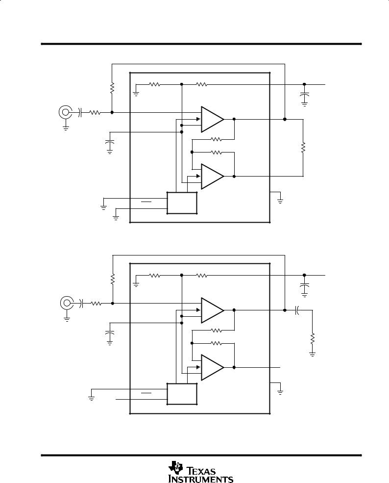
Figure 1. BTL Mode Test Circuit |
|
||
|
|
|
|
|
VDD |
6 |
|
RF |
|
|
|
|
VDD |
Audio |
|
V |
/2 |
|
CS |
|
|
|
|
||||
|
|
DD |
|
|
|
|
Input |
|
|
|
|
|
|
RI |
4 |
IN |
|
± |
VO+ |
5 |
|
|
|
|
|||
CI |
2 |
BYPASS |
|
+ |
|
|
|
|
|
CO |
|||
|
|
|
|
|||
CB |
|
|
|
|
|
|
|
|
|
|
|
|
RL = 32 Ω |
|
|
|
|
± |
VO± |
8 |
|
|
|
|
+ |
|
7 |
|
|
|
|
|
|
|
|
1 |
SHUTDOWN |
|
GND |
|
|
|
3 |
SE/BTL |
Bias |
|
|
|
VDD |
Control |
|
|
|
||
|
|
|
|
|
|
|
Figure 2. SE Mode Test Circuit
POST OFFICE BOX 655303 •DALLAS, TEXAS 75265 |
5 |
TPA711
700-mW MONO LOW-VOLTAGE AUDIO POWER AMPLIFIER
SLOS230B ± NOVEMBER 1998 ± REVISED MARCH 2000
TYPICAL CHARACTERISTICS
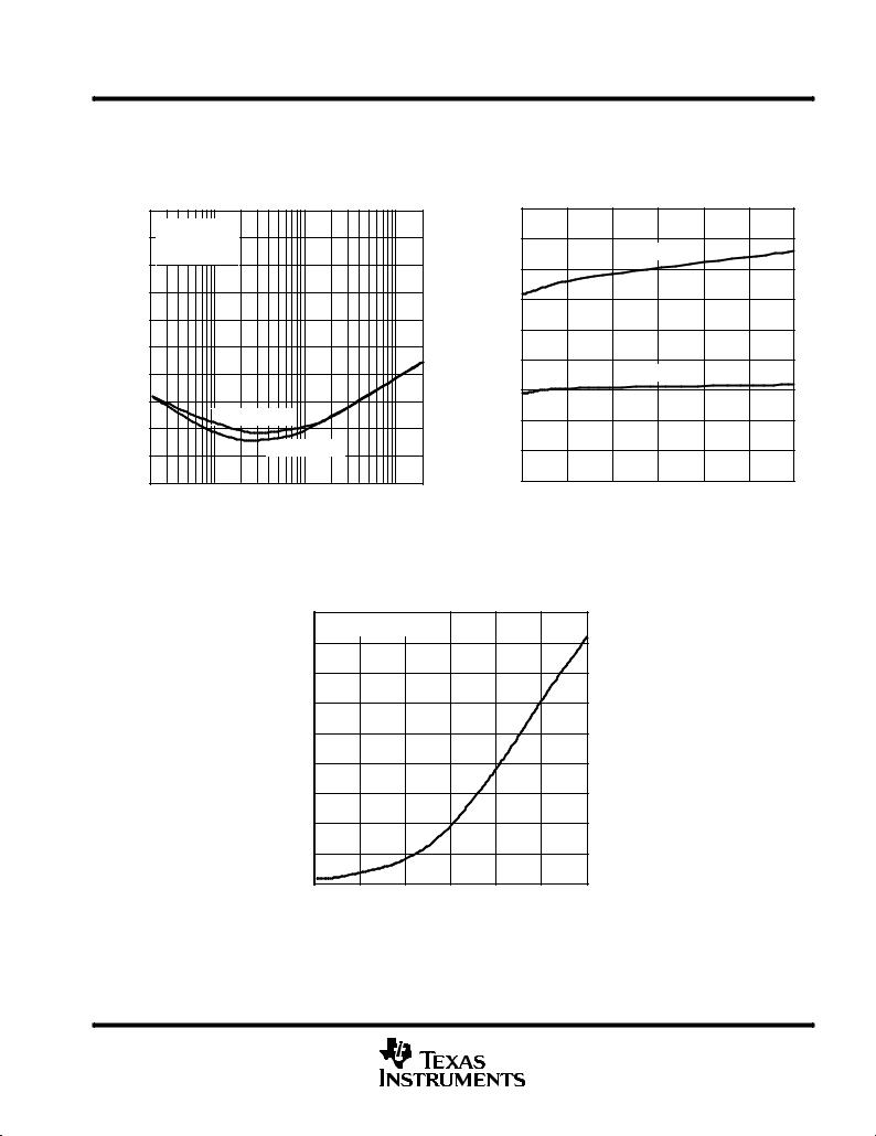
Table of Graphs
|
|
|
FIGURE |
||
|
|
|
|
||
|
Supply ripple rejection ratio |
vs Frequency |
3, 4, 5 |
||
|
|
|
|
|
|
IDD |
Supply current |
vs Supply voltage |
6, |
7 |
|
PO |
Output power |
vs Supply voltage |
8, |
9 |
|
|
|
|
|||
vs Load resistance |
10, 11 |
||||
|
|
||||
|
|
|
|
||
|
|
vs Frequency |
12, 13, 16, 17, 20, 21, |
||
|
|
24, 25, 28, 29, 32, 33 |
|||
THD + N |
Total harmonic distortion plus noise |
|
|||
|
|
|
|||
vs Output power |
14, 15, 18, 19, 22, 23, |
||||
|
|
||||
|
|
26, 27, 30, 31, 34, 35 |
|||
|
|
|
|||
|
|
|
|
|
|
|
Open loop gain and phase |
vs Frequency |
36, |
37 |
|
|
|
|
|
|
|
|
Closed loop gain and phase |
vs Frequency |
38, 39, |
40, 41 |
|
|
|
|
|
|
|
Vn |
Output noise voltage |
vs Frequency |
42, |
43 |
|
PD |
Power dissipation |
vs Output power |
44, 45, |
46, 47 |
|
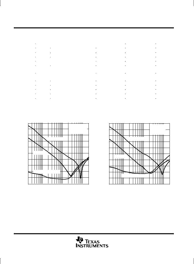
SUPPLY RIPPLE REJECTION RATIO SUPPLY RIPPLE REJECTION RATIO
|
|
|
vs |
|
|
|
|
|
|
FREQUENCY |
|
|
|
|
0 |
|
|
VDD = 3.3 V |
|
0 |
|
|
|
|
|
|
|
± dB |
±10 |
|
|
RL = 8 Ω |
± dB |
±10 |
±20 |
|
|
SE |
|
||
|
|
|
±20 |
|||
Ratio |
±30 |
|
CB = 0.1 µF |
|
Ratio |
±30 |
|
|
|
||||
Rejection |
±40 |
|
|
|
Rejection |
±40 |
±50 |
CB = 1 µF |
|
|
±50 |
||
Ripple |
±60 |
|
|
|
Ripple |
±60 |
|
|
|
|
|
||
Supply |
±70 |
|
|
|
Supply |
±70 |
±80 |
BYPASS = 1/2 VDD |
|
±80 |
|||
|
|
|
|
|||
|
±90 |
|
|
|
|
±90 |
|
±100 |
100 |
1k |
10k |
20k |
±100 |
|
20 |
|
||||
|
|
|
f ± Frequency ± Hz |
|
|
|
|
|
vs |
|
|
|
|
FREQUENCY |
|
|
|
|
|
VDD = 5 V |
|
|
|
|
RL = 8 Ω |
|
|
|
|
SE |
|
|
|
CB = 0.1 µF |
|
|
|
CB = 1 µF |
|
|
|
|
BYPASS = 1/2 VDD |
|
|
|
20 |
100 |
1k |
10k |
20k |
|
|
f ± Frequency ± Hz |
|
|
Figure 3 |
Figure 4 |
6 |
POST OFFICE BOX 655303 •DALLAS, TEXAS 75265 |
TPA711 700-mW MONO LOW-VOLTAGE AUDIO POWER AMPLIFIER
SLOS230B ± NOVEMBER 1998 ± REVISED MARCH 2000
TYPICAL CHARACTERISTICS
SUPPLY RIPPLE REJECTION RATIO |
SUPPLY CURRENT |
|
|
|
vs |
|
|
|
|
|
vs |
|
|
|
|
|
|
FREQUENCY |
|
|
|
|
SUPPLY VOLTAGE |
|
|
||
|
0 |
|
|
|
|
1.8 |
|
|
|
|
|
|
|
±10 |
RL = 8 Ω |
|
|
|
|
|
|
|
|
|
|
dB |
CB = 1 µF |
|
|
|
1.6 |
|
|
BTL |
|
|
|
|
|
BTL |
|
|
|
|
|
|
|
|
|
||
± |
±20 |
|
|
|
|
|
|
|
|
|
|
|
|
|
|
|
1.4 |
|
|
|
|
|
|
||
Ratio |
|
|
|
|
|
|
|
|
|
|
||
|
|
|
|
|
|
|
|
|
|
|
||
±30 |
|
|
|
mA |
1.2 |
|
|
|
|
|
|
|
Rejection |
|
|
|
|
Current± |
|
|
|
|
|
|
|
±50 |
|
|
|
|
|
|
|
|
|
|
||
|
±40 |
|
|
|
|
1 |
|
|
|
|
|
|
Ripple |
|
|
|
|
Supply |
|
|
|
|
|
|
|
±60 |
|
|
|
0.8 |
|
|
SE |
|
|
|
||
|
|
|
|
|
|
|
|
|
|
|||
|
|
|
|
|
|
|
|
|
|
|
||
Supply |
±70 |
|
|
|
I |
0.6 |
|
|
|
|
|
|
|
|
|
|
± |
|
|
|
|
|
|
|
|
|
±80 |
VDD = 3.3 V |
|
DD |
0.4 |
|
|
|
|
|
|
|
|
|
|
|
|
|
|
|
|
|
|
|
|
|
±90 |
|
VDD = 5 V |
|
|
0.2 |
|
|
|
|
|
|
|
|
|
|
|
|
|
|
|
|
|
|
|
|
±100 |
|
|
|
|
0 |
3 |
3.5 |
|
|
|
5.5 |
|
20 |
100 |
1k |
10k |
20k |
2.5 |
4 |
4.5 |
5 |
|||
|
|
|
f ± Frequency ± Hz |
|
|
|
|
VDD ± Supply Voltage ± V |
|
|
||
Figure 5 |
Figure 6 |
SUPPLY CURRENT vs
SUPPLY VOLTAGE
90 
 SHUTDOWN = High
|
80 |
|
|
|
|
|
|
± A |
70 |
|
|
|
|
|
|
60 |
|
|
|
|
|
|
|
Current |
|
|
|
|
|
|
|
50 |
|
|
|
|
|
|
|
|
|
|
|
|
|
|
|
± Supply |
40 |
|
|
|
|
|
|
30 |
|
|
|
|
|
|
|
DD |
|
|
|
|
|
|
|
I |
20 |
|
|
|
|
|
|
|
|
|
|
|
|
|
|
|
10 |
|
|
|
|
|
|
|
0 |
|
|
|
|
|
|
|
2.5 |
3 |
3.5 |
4 |
4.5 |
5 |
5.5 |
|
|
|
VDD ± Supply Voltage ± V |
|
|
||
Figure 7
POST OFFICE BOX 655303 •DALLAS, TEXAS 75265 |
7 |
TPA711
700-mW MONO LOW-VOLTAGE AUDIO POWER AMPLIFIER
SLOS230B ± NOVEMBER 1998 ± REVISED MARCH 2000
TYPICAL CHARACTERISTICS
OUTPUT POWER |
OUTPUT POWER |
vs |
vs |
SUPPLY VOLTAGE |
SUPPLY VOLTAGE |
|
1000 |
THD+N 1% |
|
|
|
|
350 |
|
|
|
|
|
|
|
|
|
|
|
|
|
|
THD+N = 1% |
|
|
|
|
|||
|
|
f = 1 kHz |
|
|
|
|
|
|
|
|
|
|
||
|
|
|
|
|
|
|
|
f = 1 kHz |
|
|
|
|
||
|
|
BTL |
|
|
|
|
|
300 |
|
|
|
|
||
|
800 |
|
|
|
|
|
SE |
|
|
|
|
|
||
|
|
|
|
|
|
|
|
|
|
|
|
|
||
|
|
|
|
|
|
|
|
|
|
|
|
|
|
|
mW |
|
|
|
|
|
|
mW |
250 |
|
|
|
|
|
|
± |
|
|
RL = 8 Ω |
|
|
|
± |
|
|
|
|
|
|
|
Power |
600 |
|
|
|
|
Power |
200 |
|
|
|
|
|
|
|
|
|
|
|
|
|
|
|
|
|
|
|
|
||
Output± |
|
|
|
|
|
|
Output± |
|
|
|
|
|
|
|
|
|
|
|
|
|
|
|
RL = 8 Ω |
|
|
|
|
||
|
|
|
|
|
|
|
|
|
|
|
|
|
|
|
|
400 |
|
|
|
|
|
|
150 |
|
|
|
|
|
|
|
|
|
|
|
|
|
|
|
|
|
|
|
|
|
O |
|
|
|
RL = 32 Ω |
|
|
O |
100 |
|
|
|
|
|
|
P |
|
|
|
|
|
|
P |
|
|
RL = 32 Ω |
|
|
|
|
|
200 |
|
|
|
|
|
|
|
|
|
|
|
|
|
|
|
|
|
|
|
|
|
|
|
|
|
|
|
|
|
|
|
|
|
|
|
|
50 |
|
|
|
|
|
|
|
0 |
|
|
|
|
|
|
0 |
|
|
|
|
|
|
|
2.5 |
3 |
3.5 |
4 |
4.5 |
5 |
5.5 |
2.5 |
3 |
3.5 |
4 |
4.5 |
5 |
5.5 |
|
|
|
VDD ± Supply Voltage ± V |
|
|
|
|
V ± Supply Voltage ± V |
|
|
||||
|
|
|
|
|
|
|
|
|
|
DD |
|
|
|
|
Figure 8 |
Figure 9 |
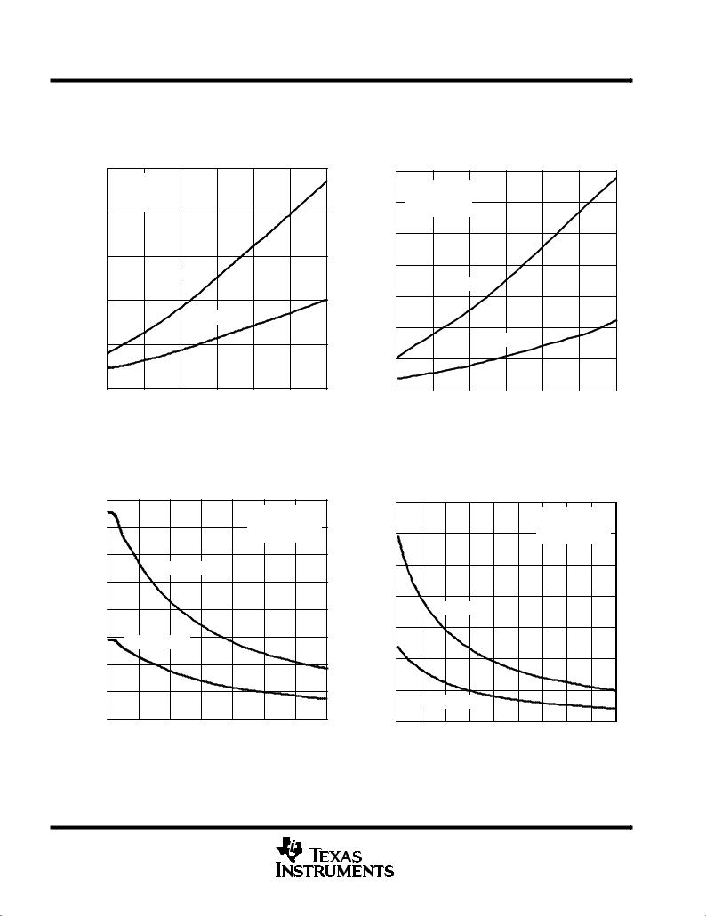
OUTPUT POWER |
OUTPUT POWER |
vs |
vs |
LOAD RESISTANCE |
LOAD RESISTANCE |
|
800 |
|
|
|
|
THD+N = 1% |
|
350 |
|
|
|
|
|
|
|
|
|
||
|
700 |
|
|
|
|
f = 1 kHz |
|
|
|
|
|
|
|
|
BTL |
|
|
300 |
|
|
|
|
|
|
|
|
|
||
mW |
600 |
|
|
|
|
|
|
mW |
250 |
|
|
VDD = 5 V |
|
|
|
|
|||
± |
500 |
|
|
|
|
|
|
± |
|
Power |
|
|
|
|
|
|
Power |
|
|
|
|
|
|
|
|
|
200 |
||
400 |
|
|
|
|
|
|
|
||
Output |
|
|
|
|
|
|
Output |
|
|
|
|
|
|
|
|
|
150 |
||
300 |
VDD = 3.3 V |
|
|
|
|
|
|||
± |
|
|
|
|
|
± |
|
||
O |
|
|
|
|
|
|
|
O |
100 |
P |
200 |
|
|
|
|
|
|
P |
|
|
|
|
|
|
|
|
|
|
|
|
100 |
|
|
|
|
|
|
|
50 |
|
0 |
16 |
24 |
32 |
40 |
48 |
56 |
64 |
0 |
|
8 |
|
|||||||
|
|
|
RL ± Load Resistance ± Ω |
|
|
|
|||
|
|
|
|
|
|
THD+N = 1% |
|
||
|
|
|
|
|
|
f = 1 kHz |
|
|
|
|
|
|
|
|
|
SE |
|
|
|
|
|
VDD = 5 V |
|
|
|
|
|
|
|
|
VDD = 3.3 V |
|
|
|
|
|
|
||
8 |
14 |
20 |
26 |
32 |
38 |
44 |
50 |
56 |
62 |
|
|
|
RL ± Load Resistance ± Ω |
|
|
||||
Figure 10 |
Figure 11 |
8 |
POST OFFICE BOX 655303 •DALLAS, TEXAS 75265 |
TPA711 700-mW MONO LOW-VOLTAGE AUDIO POWER AMPLIFIER
SLOS230B ± NOVEMBER 1998 ± REVISED MARCH 2000
TYPICAL CHARACTERISTICS
TOTAL HARMONIC DISTORTION PLUS NOISE |
TOTAL HARMONIC DISTORTION PLUS NOISE |
|
|
vs |
|
|
|
|
|
vs |
|
|
10 |
|
FREQUENCY |
|
|
|
|
|
FREQUENCY |
|
|
|
|
|
|
|
10 |
|
|
|
|
|
Noise+DistortionHarmonic±TotalTHD+N± % |
VDD = 3.3 V |
|
|
|
Noise+DistortionHarmonic±TotalTHD+N± % |
VDD = 3.3 V |
|
|
|
|
PO = 250 mW |
|
|
RL = 8 Ω |
PO = 250 mW |
|
|
||||
RL = 8 Ω |
|
|
|
A |
= ±2 V/V |
|
|
|||
|
BTL |
|
|
|
|
V |
|
|
|
|
|
AV =± 20 V/V |
|
|
|
BTL |
|
|
|
||
|
|
|
|
|
|
|
|
|||
|
|
|
|
|
|
|
|
|
|
|
1 |
|
|
|
|
|
1 |
|
PO = 50 mW |
|
|
|
AV = ±10 V/V |
|
|
|
|
|
|
|
|
|
0.1 |
|
|
AV = ±2 V/V |
|
|
0.1 |
|
|
|
|
|
|
|
|
|
|
PO = 125 mW |
|
|||
|
|
|
|
|
|
|
|
|||
|
|
|
|
|
|
|
|
|
||
0.01 |
|
|
|
|
|
0.01 |
|
|
|
|
20 |
100 |
1k |
10k |
20k |
|
|
|
|
|
|
|
20 |
100 |
1k |
10k |
20k |
|||||
|
|
|
|
|
|
|||||
|
|
f ± Frequency ± Hz |
|
|
|
|
f ± Frequency ± Hz |
|
|
|
Figure 12 |
Figure 13 |
TOTAL HARMONIC DISTORTION PLUS NOISE |
TOTAL HARMONIC DISTORTION PLUS NOISE |
|
|
|
|
vs |
|
|
|
|
|
vs |
|
|
|
|
OUTPUT POWER |
|
|
|
|
OUTPUT POWER |
|
||
10 |
VDD = 3.3 V |
|
|
|
|
|
10 |
|
|
||
DistortionHarmonic±TotalTHD+N+ Noise ± % |
|
|
|
|
|
DistortionHarmonic±TotalTHD+N+ Noise ± % |
|
|
|||
f = 1 kHz |
|
|
|
|
|
|
|
|
|||
AV = ±2 V/V |
|
|
|
|
|
|
|
||||
BTL |
|
|
|
|
|
|
|
f = 20 kHz |
|
||
|
|
|
|
|
|
|
|
|
|||
|
|
|
|
|
|
|
|
f = 10 kHz |
|
||
1 |
|
|
|
|
|
|
|
|
1 |
|
|
|
|
|
RL = 8 Ω |
|
|
|
|
|
f = 1 kHz |
|
|
|
|
|
|
|
|
|
|
|
|
||
0.1 |
|
|
|
|
|
|
|
|
0.1 |
f = 20 Hz |
|
|
|
|
|
|
|
|
|
|
|
VDD = 3.3 V |
|
|
|
|
|
|
|
|
|
|
|
|
RL = 8 Ω |
|
|
|
|
|
|
|
|
|
|
|
CB = 1 µF |
|
|
|
|
|
|
|
|
|
|
|
AV = ±2 V/V |
|
|
|
|
|
|
|
|
|
|
|
BTL |
0.01 |
|
|
|
|
|
|
|
|
0.01 |
|
|
0 |
0.05 |
0.1 |
0.15 |
0.2 |
0.25 |
0.3 |
0.35 |
0.4 |
0.01 |
0.1 |
1 |
|
|
PO ± Output Power ± W |
|
|
|
P ± Output Power ± W |
|||||
|
|
|
|
|
|
|
|
|
|
O |
|
|
|
|
Figure 14 |
|
|
|
|
|
Figure 15 |
|
|
POST OFFICE BOX 655303 •DALLAS, TEXAS 75265 |
9 |

TPA711
700-mW MONO LOW-VOLTAGE AUDIO POWER AMPLIFIER
SLOS230B ± NOVEMBER 1998 ± REVISED MARCH 2000
TYPICAL CHARACTERISTICS
TOTAL HARMONIC DISTORTION PLUS NOISE |
TOTAL HARMONIC DISTORTION PLUS NOISE |
|
|
|
vs |
|
|
|
|
|
vs |
|
|
|
|
|
FREQUENCY |
|
|
|
|
|
FREQUENCY |
|
|
% |
10 |
VDD = 5 V |
|
|
|
% |
10 |
|
|
|
|
|
|
|
|
|
VDD = 5 V |
|
|
|
|||
± |
|
PO = 700 mW |
|
|
± |
|
RL = 8 Ω |
|
|
|
|
Noise |
|
|
|
Noise |
|
|
|
|
|||
|
RL = 8 Ω |
AV = ±20 V/V |
|
|
|
BTL |
|
|
|
||
|
|
BTL |
|
|
|
|
|
AV = ±2 V/V |
|
PO = 50 mW |
|
+ |
|
|
|
|
|
+ |
|
|
|
|
|
Distortion |
1 |
|
|
|
|
Distortion |
1 |
|
|
|
|
Harmonic |
0.1 |
|
AV = ±2 V/V |
|
Harmonic |
0.1 |
PO = 700 mW |
|
|
||
±TotalTHD+N |
|
AV = ±10 V/V |
|
|
±TotalTHD+N |
|
|
|
|
|
|
|
|
|
|
|
|
|
PO = 350 mW |
|
|||
|
|
|
|
|
|
|
|
|
|
||
|
0.01 |
|
|
|
|
|
0.01 |
|
|
|
|
|
20 |
100 |
1k |
10k |
20k |
|
20 |
100 |
1k |
10k |
20k |
|
|
|
f ± Frequency ± Hz |
|
|
|
|
|
f ± Frequency ± Hz |
|
|
Figure 16 |
Figure 17 |
TOTAL HARMONIC DISTORTION PLUS NOISE |
TOTAL HARMONIC DISTORTION PLUS NOISE |
vs |
vs |
OUTPUT POWER |
OUTPUT POWER |
% |
10 |
|
|
|
|
|
|
|
|
|
% |
10 |
|
|
|
VDD = 5 V |
|
|
|
|
|
|
|
|
|
|
|||
± |
|
|
|
|
|
|
|
|
± |
|
|
|
||
|
f = 1 kHz |
|
|
|
|
|
|
|
|
|
|
|||
Noise |
|
|
|
|
|
|
|
|
Noise |
|
|
|
||
|
AV |
= ±2 V/V |
|
|
|
|
|
|
|
|
|
|
||
+ |
|
BTL |
|
|
|
|
|
|
|
+ |
|
|
|
|
|
|
|
|
|
|
|
|
|
|
|
|
|
||
Distortion |
1 |
|
|
|
|
|
|
|
|
|
Distortion |
1 |
f = 20 kHz |
|
|
|
|
|
|
|
|
|
|
|
|
|
|||
|
|
|
|
|
|
|
|
|
|
|
f = 10 kHz |
|
||
Harmonic |
|
|
|
|
|
|
|
|
|
|
Harmonic |
|
|
|
0.1 |
|
|
|
RL = 8 Ω |
|
|
|
|
0.1 |
f = 1 kHz |
|
|||
|
|
|
|
|
|
|
|
|
|
|
|
|||
|
|
|
|
|
|
|
|
|
|
|
f = 20 Hz |
|
||
±Total |
|
|
|
|
|
|
|
|
|
|
±Total |
|
|
|
|
|
|
|
|
|
|
|
|
|
VDD = 5 V |
|
|||
THD+N |
|
|
|
|
|
|
|
|
|
|
THD+N |
RL = 8 Ω |
|
|
|
|
|
|
|
|
|
|
|
|
CB = 1 |
µF |
|
||
|
|
|
|
|
|
|
|
|
|
|
|
AV = ±2 V/V |
|
|
|
0.01 |
|
|
|
|
|
|
|
|
|
|
BTL |
|
|
|
|
|
|
|
|
|
|
|
|
|
0.01 |
|
|
|
|
0.1 |
0.2 |
0.3 |
0.4 |
0.5 |
0.6 |
0.7 |
0.8 |
0.9 |
1 |
|
0.01 |
0.1 |
1 |
|
|
|
PO ± Output Power ± W |
|
|
|
|
|
PO ± Output Power ± W |
|
||||
Figure 18 |
Figure 19 |
10 |
POST OFFICE BOX 655303 •DALLAS, TEXAS 75265 |
 Loading...