


TPS2816DBVR
Texas Instruments TPS2816DBVR, TPS2816DBV, TPS2829DBVR, TPS2829DBV, TPS2828DBVT Datasheet
...
TPS2816, TPS2817, TPS2818, TPS2819, TPS2828, TPS2829
SINGLE-CHANNEL HIGH-SPEED MOSFET DRIVER
SLVS160A – FEBRUARY 1997 – REVISED NOVEMBER 1997
1
POST OFFICE BOX 655303 • DALLAS, TEXAS 75265
D
Low-Cost Single-Channel High-Speed
MOSFET Driver
D
ICC...15-µA Max (TPS2828, TPS2829)
D
25-ns Max Rise/Fall Times and 40-ns Max
Propagation Delay...1-nF Load
D
2-A Peak Output Current
D
4-V to 14-V Driver Supply Voltage Range;
Internal Regulator Extends Range to 40 V
(TPS2816, TPS2817, TPS2818, TPS2819)
D
5-pin SOT-23 Package
D
–40°C to 125°C Ambient-Temperature
Operating Range
D
Highly Resistant to Latch-ups
description
The TPS28xx single-channel high-speed MOSFET drivers are capable of delivering peak
currents of up to 2 A into highly capacitive loads.
High switching speeds (t
r
and tf = 14 ns typ) are
obtained with the use of BiCMOS outputs. Typical
threshold switching voltages are 2/3 and 1/3 of
V
CC
. The design inherently minimizes shoot-
through current.
A regulator is provided on TPS2816 through TPS2819 devices to allow operation with supply inputs between
14 V and 40 V. The regulator output can be used to power other circuits, provided power dissipation does not
exceed package limitations. If the regulator is not required, V
DD
(the regulator input) should be connected to
V
CC
. The TPS2816 and TPS2817 input circuits include an active pullup circuit to eliminate the need for an
external resistor when using open-collector PWM controllers. The TPS2818 and TPS2819 are identical to the
TPS2816 and TPS2817, except that the active pullup circuit is omitted. The TPS2828 and TPS2829 are
identical to the TPS2818 and TPS2819, except that the internal voltage regulator is omitted, allowing quiescent
current to drop to less than 15 µA when the inputs are high or low.
The TPS28xx series devices are available in 5-pin SOT-23 (DBV) packages and operate over an ambient
temperature range of –40_C to 125_C.
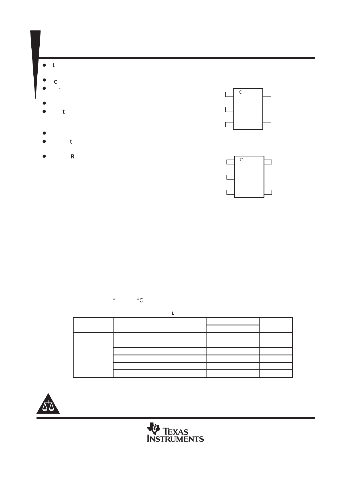
AVAILABLE OPTIONS
PACKAGED DEVICES
CHIP FORM
T
A
FUNCTION
SOT-23–5 (DBV)
(Y)
Inverting driver with active pullup input TPS2816DBV TPS2816Y
Noninverting driver with active pullup input TPS2817DBV TPS2817Y
°
°
Inverting driver TPS2818DBV TPS2818Y
–
40°C to 125°C
Noninverting driver TPS2819DBV TPS2819Y
Inverting driver, no regulator TPS2828DBV TPS2828Y
Noninverting driver, no regulator TPS2829DBV TPS2829Y
The DBV package is available taped and reeled only.
Copyright 1997, Texas Instruments Incorporated
PRODUCTION DATA information is current as of publication date.
Products conform to specifications per the terms of Texas Instruments
standard warranty. Production processing does not necessarily include
testing of all parameters.
Please be aware that an important notice concerning availability, standard warranty, and use in critical applications of
Texas Instruments semiconductor products and disclaimers thereto appears at the end of this data sheet.
3
2
1
4
5
IN
V
CC
V
DD
OUT
TPS2816, TPS2817
TPS2818, TPS2819
DBV PACKAGE
(TOP VIEW)
GND
3
2
1
4
5
IN
V
CC
NC
OUT
DBV PACKAGE
(TOP VIEW)
GND
TPS2828, TPS2829
NC – No internal connection
TPS2816, TPS2817, TPS2818, TPS2819, TPS2828, TPS2829
SINGLE-CHANNEL HIGH-SPEED MOSFET DRIVER
SLVS160A – FEBRUARY 1997 – REVISED NOVEMBER 1997
2
POST OFFICE BOX 655303 • DALLAS, TEXAS 75265
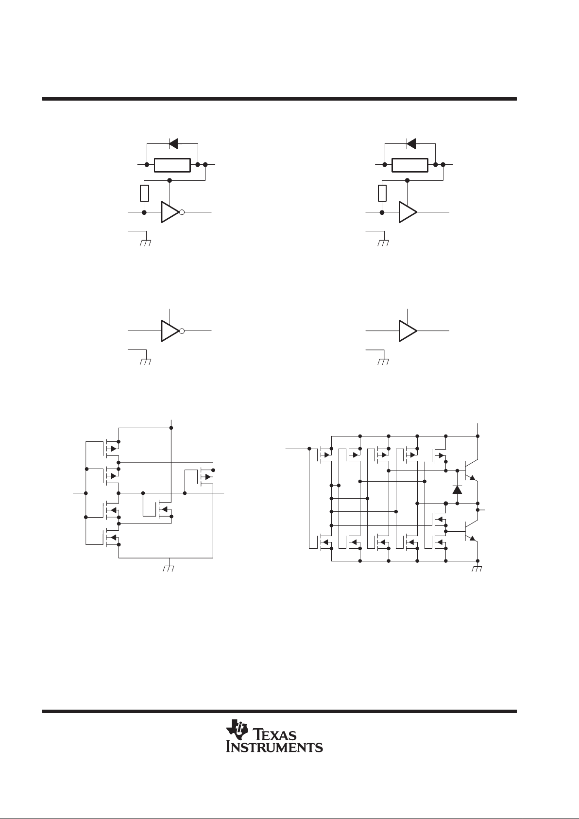
functional block diagram
VREG
V
DD
IN
GND
V
CC
OUT
TPS2816, TPS2818
Active Pullup
(TPS2816 Only)
VREG
V
DD
IN
GND
V
CC
OUT
TPS2817, TPS2819
Active Pullup
(TPS2817 Only)
IN
GND
OUT
TPS2828
IN
GND
OUT
TPS2829
V
CC
V
CC
INPUT STAGE DIAGRAM
To Drive
Stage
IN
V
CC
OUTPUT STAGE DIAGRAM
V
CC
OUT
Predrive
TPS2816, TPS2817, TPS2818, TPS2819, TPS2828, TPS2829
SINGLE-CHANNEL HIGH-SPEED MOSFET DRIVER
SLVS160A – FEBRUARY 1997 – REVISED NOVEMBER 1997
3
POST OFFICE BOX 655303 • DALLAS, TEXAS 75265
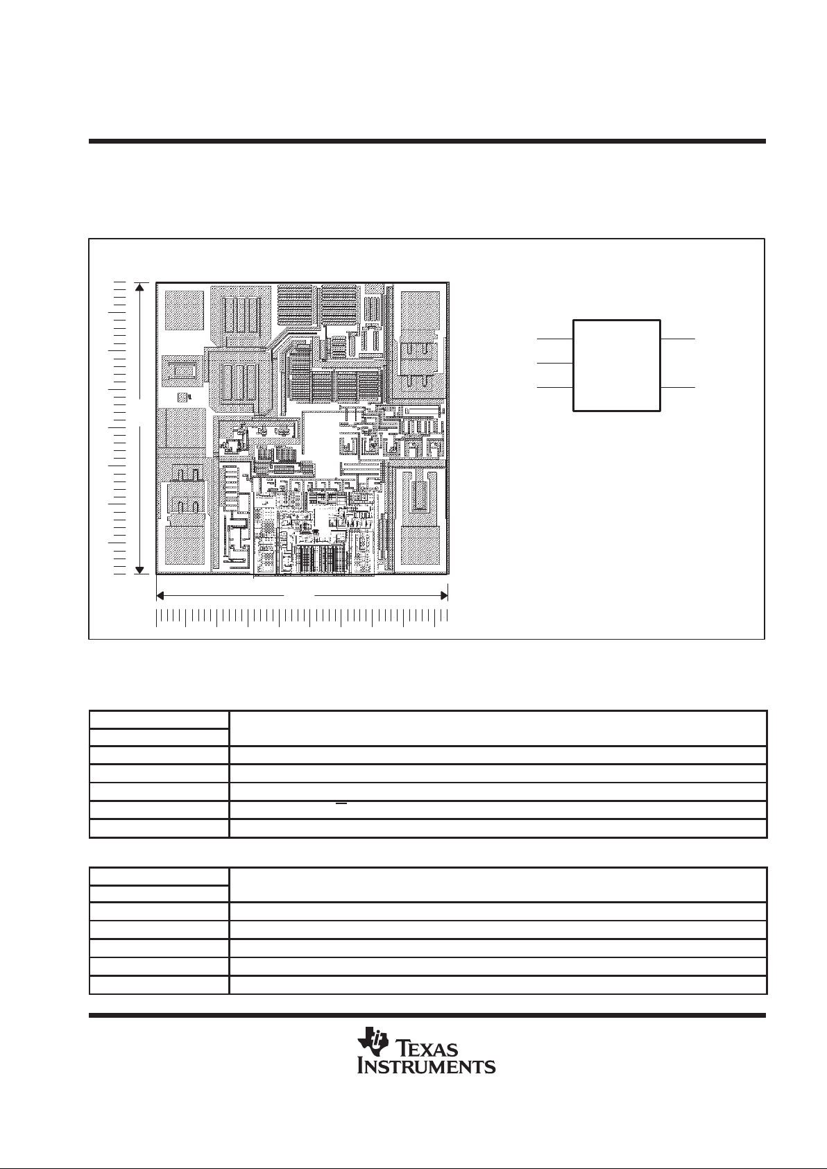
TPS28xxY chip information
This chip, when properly assembled, displays characteristics similar to those of the TPS28xx. Thermal
compression or ultrasonic bonding may be used on the doped aluminum bonding pads. The chip may be
mounted with conductive epoxy or a gold-silicon preform.
39
39
TPS2816Y
(4)
(2)
(3)
(5)
(1)
OUT
GND
IN
V
CC
V
DD
†
BONDING PAD ASSIGNMENTS
CHIP THICKNESS: 15 TYPICAL
BONDING PADS: 4 × 4 MINIMUM
TJ max = 150°C
TOLERANCES ARE ±10%.
ALL DIMENSIONS ARE IN MILS.
(4)
(2)
(3)
(1)
(5)
†
TPS2816 through TPS2819 only
Terminal Functions
TPS2816, TPS2818, TPS2828 (inverting driver)
TERMINAL
NAME NO.
DESCRIPTION
V
DD
1 Regulator supply voltage input. (Not connected on TPS2828)
GND 2 Ground
IN 3 Driver input.
OUT 4 Driver output, OUT = IN
V
CC
5 Driver supply voltage/regulator output voltage
TPS2817, TPS2819, TPS2829 (noninverting driver)
TERMINAL
NAME NO.
DESCRIPTION
V
DD
1 Regulator supply voltage input. (Not connected on TPS2829)
GND 2 Ground
IN 3 Driver input.
OUT 4 Driver output, OUT= IN
V
CC
5 Driver supply voltage/regulator output voltage
TPS2816, TPS2817, TPS2818, TPS2819, TPS2828, TPS2829
SINGLE-CHANNEL HIGH-SPEED MOSFET DRIVER
SLVS160A – FEBRUARY 1997 – REVISED NOVEMBER 1997
4
POST OFFICE BOX 655303 • DALLAS, TEXAS 75265
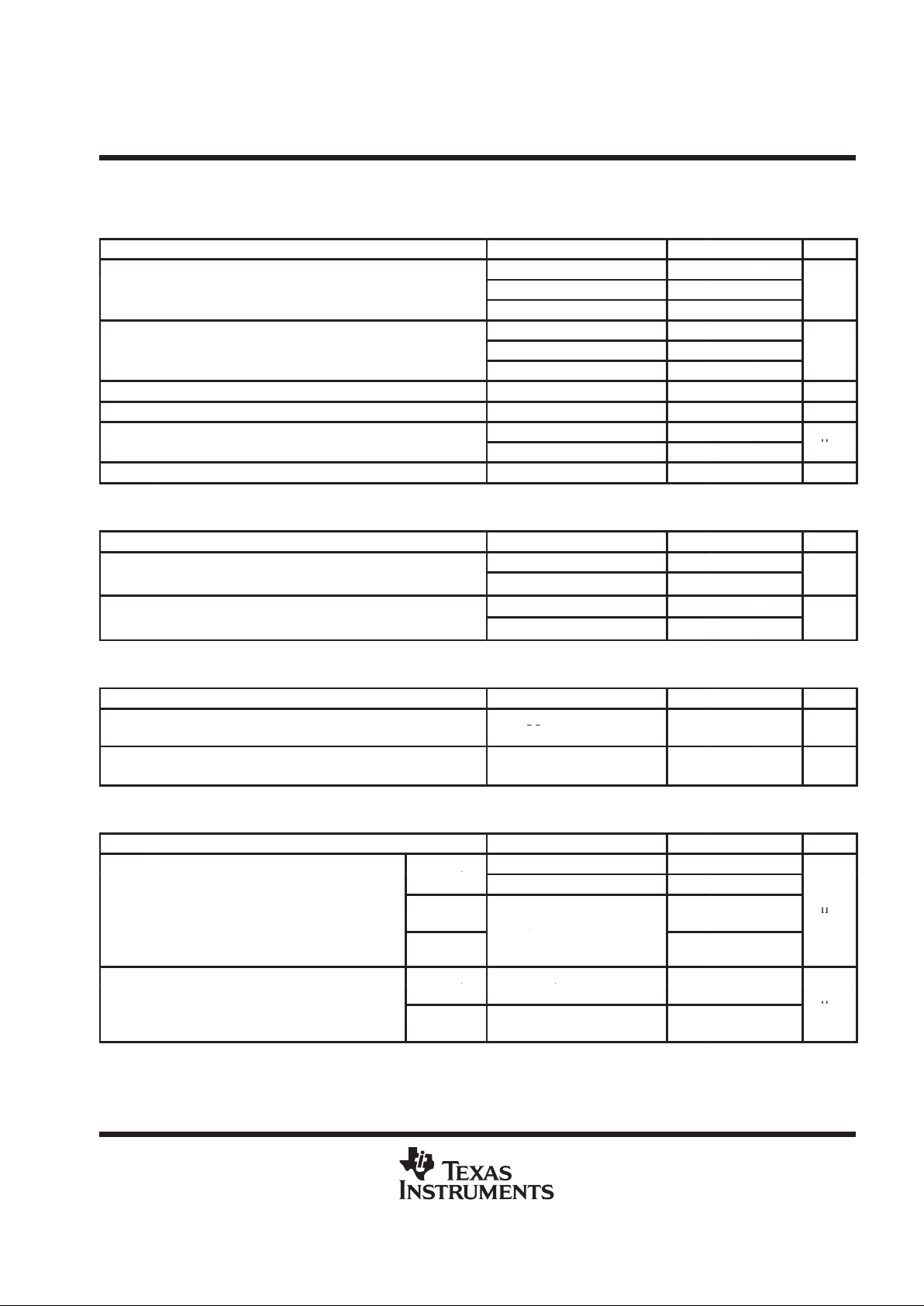
DISSIPATION RATING TABLE
PACKAGE
TA ≤ 25°C
POWER RATING
DERATING FACTOR
ABOVE TA = 25°C
TA = 70°C
POWER RATING
TA = 80°C
POWER RATING
DBV 437 mW 3.5 mW/°C 280 mW 227 mW
These dissipation ratings are based upon EIA specification JESD51-3, ”Low Effective Thermal
Conductivity T est Board for Leaded Surface Mount Packages,” in tests conducted in a zero-airflow , wind
tunnel environment.
absolute maximum ratings over operating temperature range (unless otherwise noted)
†
Regulator supply voltage range, V
DD
–0.3 V to 42 V. . . . . . . . . . . . . . . . . . . . . . . . . . . . . . . . . . . . . . . . . . . . . . . .
Supply voltage range, V
CC
–0.3 V to 15 V. . . . . . . . . . . . . . . . . . . . . . . . . . . . . . . . . . . . . . . . . . . . . . . . . . . . . . . . .
Input voltage range, IN –0.3 V to 15 V. . . . . . . . . . . . . . . . . . . . . . . . . . . . . . . . . . . . . . . . . . . . . . . . . . . . . . . . . . . .
Continuous regulator output current, V
CC
25 mA. . . . . . . . . . . . . . . . . . . . . . . . . . . . . . . . . . . . . . . . . . . . . . . . . . .
Continuous output current, OUT ±100 mA. . . . . . . . . . . . . . . . . . . . . . . . . . . . . . . . . . . . . . . . . . . . . . . . . . . . . . . .
Continuous total power dissipation See Dissipation Rating Table. . . . . . . . . . . . . . . . . . . . . . . . . . . . . . . . . . . . . .
Operating ambient temperature range, T
A
–40°C to 125°C. . . . . . . . . . . . . . . . . . . . . . . . . . . . . . . . . . .
Storage temperature range, T
stg
–65°C to 150°C. . . . . . . . . . . . . . . . . . . . . . . . . . . . . . . . . . . . . . . . . .
Lead temperature 1,6 mm (1/16inch) from case for 10 seconds 260°C. . . . . . . . . . . . . . . . . . . . . . . . . . . . . . . . .
†
Stresses beyond those listed under “absolute maximum ratings” may cause permanent damage to the device. These are stress ratings only, and
functional operation of the device at these or any other conditions beyond those indicated under “recommended operating conditions” is not
implied. Exposure to absolute-maximum-rated conditions for extended periods may affect device reliability.
NOTE 1: All voltages are with respect to device GND terminal.
recommended operating conditions
MIN MAX UNIT
Regulator input voltage range, VDD, TPS2816 through TPS2819 8 40 V
Supply voltage, V
CC
4 14 V
Input voltage, IN –0.3 V
CC
V
Continuous regulator output current, I
CC
0 20 mA
Operating ambient temperature range, T
A
–40 125
_
C
TPS2816, TPS2817, TPS2818, TPS2819, TPS2828, TPS2829
SINGLE-CHANNEL HIGH-SPEED MOSFET DRIVER
SLVS160A – FEBRUARY 1997 – REVISED NOVEMBER 1997
5
POST OFFICE BOX 655303 • DALLAS, TEXAS 75265
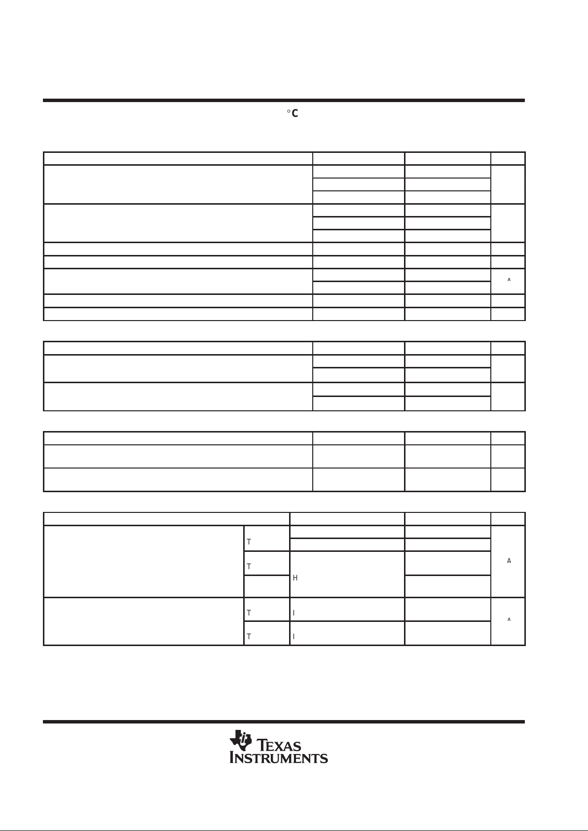
TPS28xx electrical characteristics over recommended operating ambient temperature range,
V
CC
= 10 V, VDD tied to VCC, CL = 1 nF (unless otherwise specified)
Inputs
PARAMETER TEST CONDITIONS MIN TYP†MAX UNIT
VCC = 5 V 3.3 4
Positive-going input threshold voltage
VCC = 10 V
6.6 7
V
VCC = 14 V 9.3 10
VCC = 5 V 1 1.7
Negative-going input threshold voltage
VCC = 10 V
2 3.3
V
VCC = 14 V 2.5 4.6
Input voltage hysteresis 1.3 V
Input current, TPS2818/19/28/29 Input = 0 V or V
CC
0.2 µA
p
Input = 0 V 650
Input current, TPS2816/17
Input = V
CC
15
µ
A
Input capacitance 5 10 pF
†
Typicals are for TA = 25°C unless otherwise noted.
outputs
PARAMETER TEST CONDITIONS MIN TYP†MAX UNIT
IO = –1 mA 9.75 9.9
High-l
evel output voltage
IO = –100 mA
8 9.1
V
p
IO = 1 mA 0.18 0.25
Low-level output voltage
IO = 100 mA 1 2
V
†
Typicals are for TA = 25°C unless otherwise noted.
regulator, TPS2816 through TPS2819
PARAMETER TEST CONDITIONS MIN TYP†MAX UNIT
p
14 ≤ VDD ≤ 40 V, 10 11.5 13
Output voltage
DD
0 ≤ IO ≤ 20 mA
V
p
p
IO = 10 mA, 8 10
Out ut voltage in dro out
VDD = 10 V
V
†
Typicals are for TA = 25°C unless otherwise noted.
supply current
PARAMETER TEST CONDITIONS MIN TYP†MAX UNIT
TPS2816,
IN = high = 10 V 150 250
,
TPS2817
IN = low = 0 V 650 1000
pp
TPS2818,
Su ly current into V
CC
,
TPS2819
IN = high or low,
25
50
µA
TPS2828,
TPS2829
g
High = 10 V, Low = 0 V
0.1 15
TPS2816, V
= 20 V,
pp
,
TPS2817
DD
,
IN = high = 10 V or low = 0 V
650
1000
Supply current into V
DD
TPS2818,
V
= 20 V,
µ
A
,
TPS2819
DD
,
IN = high = 10 V or low = 0 V
50
150
†
Typicals are for TA = 25°C unless otherwise noted.
TPS2816, TPS2817, TPS2818, TPS2819, TPS2828, TPS2829
SINGLE-CHANNEL HIGH-SPEED MOSFET DRIVER
SLVS160A – FEBRUARY 1997 – REVISED NOVEMBER 1997
6
POST OFFICE BOX 655303 • DALLAS, TEXAS 75265
TPS28xxY electrical characteristics at TA = 25_C, V
CC
= 10 V, VDD tied to VCC, CL = 1 nF
(unless otherwise specified)
Inputs
PARAMETER TEST CONDITIONS MIN TYP MAX UNIT
VCC = 5 V 3.3
Positive-going input threshold voltage
VCC = 10 V
6.6
V
VCC = 14 V 9.3
VCC = 5 V 1.7
Negative-going input threshold voltage
VCC = 10 V
3.3
V
VCC = 14 V 4.6
Input voltage hysteresis 1.3 V
Input current, TPS2818/19/28/29 Input = 0 V or V
CC
0.2 µA
p
Input = 0 V 650
Input current, TPS2816/17
Input = V
CC
15
µ
A
Input resistance 1000 MΩ
Input capacitance 5 pF
outputs
PARAMETER TEST CONDITIONS MIN TYP MAX UNIT
IO = –1 mA 9.9
High-l
evel output voltage
IO = –100 mA 9.1
V
p
IO = 1 mA 0.18
Low-level output voltage
IO = 100 mA 1
V
regulator, TPS2816 through TPS2819
PARAMETER TEST CONDITIONS MIN TYP MAX UNIT
Output voltage 14 ≤ VDD ≤ 40 V,
0 ≤ IO ≤ 20 mA
11.5 V
Output voltage in dropout IO = 10 mA,
VDD = 10 V
9 V
supply current
PARAMETER TEST CONDITIONS MIN TYP MAX UNIT
TPS2816,
IN = high = 10 V 150
,
TPS2817
IN = low = 0 V 650
pp
TPS2818,
Su ly current into V
CC
,
TPS2819
IN = high or low,
25
µA
TPS2828,
TPS2829
g
High = 10 V, Low = 0 V
0.1
TPS2816, V
= 20 V,
pp
,
TPS2817
DD
,
IN = high = 10 V or low = 0 V
650
Supply current into V
DD
TPS2818,
V
= 20 V,
µ
A
,
TPS2819
DD
,
IN = high = 10 V or low = 0 V
50
 Loading...