


 Loading...
Texas instruments TMS320F28031, TMS320F28032, TMS320F28034, TMS320F28033, TMS320F28035 Data Manual
...TMS320F28030, TMS320F28031, TMS320F28032
TMS320F28033, TMS320F28034, TMS320F28035
www.ti.com |
SPRS584D –APRIL 2009 –REVISED JUNE 2010 |
Piccolo Microcontrollers
Check for Samples: TMS320F28030, TMS320F28031, TMS320F28032, TMS320F28033, TMS320F28034, TMS320F28035
1 TMS320F2803x ( Piccolo™ ) MCUs
1.1Features
•Highlights
–High-Efficiency 32-Bit CPU ( TMS320C28x™ )
–60-MHz Device
–Single 3.3-V Supply
–Integrated Power-on and Brown-out Resets
–Two Internal Zero-pin Oscillators
–Up to 45 Multiplexed GPIO Pins
–Three 32-Bit CPU Timers
–On-Chip Flash, SARAM, OTP Memory
–Code-Security Module
–Serial Port Peripherals (SCI/SPI/I2C/LIN/eCAN)
–Enhanced Control Peripherals
•Enhanced Pulse Width Modulator (ePWM)
•High-Resolution PWM (HRPWM)
•Enhanced Capture (eCAP)
•Enhanced Quadrature Encoder Pulse (eQEP)
•Analog-to-Digital Converter (ADC)
•On-Chip Temperature Sensor
•Comparator
–64-Pin and 80-Pin Packages
•High-Efficiency 32-Bit CPU ( TMS320C28x™ )
–60 MHz (16.67-ns Cycle Time)
–16 x 16 and 32 x 32 MAC Operations
–16 x 16 Dual MAC
–Harvard Bus Architecture
–Atomic Operations
–Fast Interrupt Response and Processing
–Unified Memory Programming Model
–Code-Efficient (in C/C++ and Assembly)
•Programmable Control Law Accelerator (CLA)
–32-Bit Floating-Point Math Accelerator
–Executes Code Independently of the Main CPU
•Low Device and System Cost:
–Single 3.3-V Supply
–No Power Sequencing Requirement
–Integrated Power-on Reset and Brown-out Reset
–Low Power
–No Analog Support Pins
•Clocking:
–Two Internal Zero-pin Oscillators
–On-Chip Crystal Oscillator/External Clock Input
–Dynamic PLL Ratio Changes Supported
–Watchdog Timer Module
–Missing Clock Detection Circuitry
•Up to 45 Individually Programmable, Multiplexed GPIO Pins With Input Filtering
•Peripheral Interrupt Expansion (PIE) Block That Supports All Peripheral Interrupts
•Three 32-Bit CPU Timers
•Independent 16-Bit Timer in Each ePWM Module
•On-Chip Memory
–Flash, SARAM, OTP, Boot ROM Available
•128-Bit Security Key/Lock
–Protects Secure Memory Blocks
–Prevents Firmware Reverse Engineering
•Serial Port Peripherals
–One SCI (UART) Module
–Two SPI Modules
–One Inter-Integrated-Circuit (I2C) Bus
–One Local Interconnect Network (LIN) Bus
–One Enhanced Controller Area Network (eCAN) Bus
•Advanced Emulation Features
–Analysis and Breakpoint Functions
–Real-Time Debug via Hardware
•2803x Packages
–64-Pin PAG Thin Quad Flatpack (TQFP)
–80-Pin PN Low-Profile Quad Flatpack (LQFP)
•Community Resources
–TI E2E Community
–TI Embedded Processors Wiki
Please be aware that an important notice concerning availability, standard warranty, and use in critical applications of Texas
Instruments semiconductor products and disclaimers thereto appears at the end of this data sheet.
Piccolo, TMS320C28x, C28x, TMS320C2000, Code Composer Studio, XDS510 are trademarks of Texas Instruments. All other trademarks are the property of their respective owners.
PRODUCTION DATA information is |
current as of publication date. |
Copyright © 2009–2010, Texas Instruments Incorporated |
Products conform to specifications |
per the terms of the Texas |
|
Instruments standard warranty. Production processing does not necessarily include testing of all parameters.

TMS320F28030, TMS320F28031, TMS320F28032
TMS320F28033, TMS320F28034, TMS320F28035
SPRS584D–APRIL 2009 –REVISED JUNE 2010 |
www.ti.com |
1.2Description
The F2803x Piccolo™ family of microcontrollers provides the power of the C28x™ core and Control Law Accelerator (CLA) coupled with highly integrated control peripherals in low pin-count devices. This family is code-compatible with previous C28x-based code, as well as providing a high level of analog integration.
An internal voltage regulator allows for single rail operation. Enhancements have been made to the HRPWM module to allow for dual-edge control (frequency modulation). Analog comparators with internal 10-bit references have been added and can be routed directly to control the PWM outputs. The ADC
converts from 0 to 3.3-V fixed full scale range and supports ratio-metric VREFHI/VREFLO references. The ADC interface has been optimized for low overhead/latency.
1.3Getting Started
This section gives a brief overview of the steps to take when first developing for a C28x device. For more detail on each of these steps, see the following:
•Getting Started With TMS320C28x Digital Signal Controllers (literature number SPRAAM0).
•C2000 Getting Started Website (http://www.ti.com/c2000getstarted)
•TMS320F28x MCU Development and Experimenter'sKits (http://www.ti.com/f28xkits)
2 |
TMS320F2803x ( Piccolo™ ) MCUs |
Copyright © 2009–2010, Texas Instruments Incorporated |
Submit Documentation Feedback
Product Folder Link(s): TMS320F28030 TMS320F28031 TMS320F28032 TMS320F28033 TMS320F28034
TMS320F28035

TMS320F28030, TMS320F28031, TMS320F28032
TMS320F28033, TMS320F28034, TMS320F28035
www.ti.com |
|
|
|
SPRS584D –APRIL 2009 –REVISED JUNE 2010 |
|||
1 |
TMS320F2803x ( Piccolo™ ) MCUs .................. |
1 |
|
4.9 |
High-Resolution PWM (HRPWM) .................. |
78 |
|
|
1.1 |
Features .............................................. |
1 |
|
4.10 Enhanced Capture Module (eCAP1) ............... |
79 |
|
|
1.2 |
Description ........................................... |
2 |
|
4.11 Enhanced Quadrature Encoder Pulse (eQEP) ..... |
81 |
|
|
1.3 |
Getting Started ....................................... |
2 |
|
4.12 |
JTAG Port .......................................... |
83 |
2 |
Introduction .............................................. |
4 |
|
4.13 |
GPIO MUX |
84 |
|
|
|
|
|
|
|||
|
2.1 |
Pin Assignments ..................................... |
5 |
5 |
Device Support ......................................... |
89 |
|
|
2.2 |
Signal Descriptions .................................. |
7 |
|
5.1 |
Device and Development Support Tool |
|
3 |
Functional Overview .................................. |
14 |
|
|
Nomenclature ....................................... |
89 |
|
|
3.1 |
Block Diagram ...................................... |
14 |
|
5.2 |
Related Documentation ............................. |
91 |
|
3.2 |
Memory Maps ...................................... |
15 |
6 |
Electrical Specifications ............................. |
93 |
|
|
3.3 |
Brief Descriptions ................................... |
22 |
|
6.1 |
Absolute Maximum Ratings ........................ |
93 |
|
3.4 |
Register Map ....................................... |
30 |
|
6.2 |
Recommended Operating Conditions .............. |
93 |
|
3.5 |
Device Emulation Registers ........................ |
31 |
|
6.3 |
Electrical Characteristics ........................... |
94 |
|
3.6 |
Interrupts ............................................ |
32 |
|
6.4 |
Current Consumption ............................... |
95 |
|
3.7 |
VREG/BOR/POR ................................... |
36 |
|
6.5 |
Thermal Design Considerations .................... |
99 |
|
3.8 |
System Control ..................................... |
38 |
|
6.6 |
Emulator Connection Without Signal Buffering for |
|
|
3.9 |
Low-power Modes Block ........................... |
46 |
|
|
the MCU ............................................ |
99 |
4 |
Peripherals .............................................. |
47 |
|
6.7 |
Timing Parameter Symbology ..................... |
100 |
|
|
4.1 |
Control Law Accelerator (CLA) Overview .......... |
47 |
|
6.8 |
Clock Requirements and Characteristics ......... |
102 |
|
4.2 |
Analog Block ........................................ |
50 |
|
6.9 |
Power Sequencing ................................ |
103 |
|
4.3 |
Serial Peripheral Interface (SPI) Module ........... |
56 |
|
6.10 |
General-Purpose Input/Output (GPIO) ............ |
105 |
|
4.4 |
Serial Communications Interface (SCI) Module .... |
59 |
|
6.11 |
Enhanced Control Peripherals .................... |
112 |
|
4.5 |
Local Interconnect Network (LIN) .................. |
62 |
|
6.12 |
Detailed Descriptions .............................. |
129 |
|
4.6 |
Enhanced Controller Area Network (eCAN) Module |
|
|
6.13 |
Flash Timing ....................................... |
130 |
|
|
...................................................... |
65 |
7 |
C-to-D Revision History ............................. |
132 |
|
|
4.7 |
Inter-Integrated Circuit (I2C) ........................ |
69 |
8 |
B-to-C Revision History ............................. |
134 |
|
|
4.8 |
Enhanced PWM Modules (ePWM1/2/3/4/5/6/7) .... |
71 |
9 |
Thermal/Mechanical Data .......................... |
137 |
|
|
|
|
|
|
|
|
|
Copyright © 2009–2010, Texas Instruments Incorporated |
Contents |
3 |
Submit Documentation Feedback
Product Folder Link(s): TMS320F28030 TMS320F28031 TMS320F28032 TMS320F28033 TMS320F28034
TMS320F28035

TMS320F28030, TMS320F28031, TMS320F28032
TMS320F28033, TMS320F28034, TMS320F28035
SPRS584D–APRIL 2009 –REVISED JUNE 2010 |
www.ti.com |
2 Introduction
Table 2-1 lists the features of the TMS320F2803x devices.
Table 2-1. Hardware Features
FEATURE |
TYPE(1) |
28030 |
28031 |
28032 |
28033 |
28034 |
28035 |
||||||||||||||
|
|
|
|
(60 MHz) |
(60 MHz) |
(60 MHz) |
(60 MHz) |
(60 MHz) |
(60 MHz) |
||||||||||||
|
|
|
|
64-Pin |
|
80-Pin |
64-Pin |
|
80-Pin |
64-Pin |
|
80-Pin |
64-Pin |
|
80-Pin |
64-Pin |
|
80-Pin |
64-Pin |
|
80-Pin |
Package Type |
|
|
PAG |
|
PN |
PAG |
|
PN |
PAG |
|
PN |
PAG |
|
PN |
PAG |
|
PN |
PAG |
|
PN |
|
|
|
|
|
TQFP |
|
LQFP |
TQFP |
|
LQFP |
TQFP |
|
LQFP |
TQFP |
|
LQFP |
TQFP |
|
LQFP |
TQFP |
|
LQFP |
Instruction cycle |
– |
16.67 ns |
16.67 ns |
16.67 ns |
16.67 ns |
16.67 ns |
16.67 ns |
||||||||||||||
Control Law Accelerator |
0 |
|
No |
|
No |
|
No |
|
Yes |
|
No |
|
Yes |
||||||||
On-chip flash (16-bit word) |
– |
|
16K |
|
32K |
|
32K |
|
32K |
|
64K |
|
64K |
||||||||
On-chip SARAM (16-bit word) |
– |
|
6K |
|
8K |
|
10K |
|
10K |
|
10K |
|
10K |
||||||||
|
|
|
|
|
|
|
|
|
|
|
|
|
|
|
|
|
|
|
|
||
Code security for on-chip |
– |
|
Yes |
|
Yes |
|
Yes |
|
Yes |
|
Yes |
|
Yes |
||||||||
flash/SARAM/OTP blocks |
|
|
|
|
|
|
|||||||||||||||
|
|
|
|
|
|
|
|
|
|
|
|
|
|
|
|
|
|
|
|||
Boot ROM (8K x 16) |
– |
|
Yes |
|
Yes |
|
Yes |
|
Yes |
|
Yes |
|
Yes |
||||||||
One-time programmable (OTP) ROM |
– |
|
1K |
|
1K |
|
1K |
|
1K |
|
1K |
|
1K |
||||||||
(16-bit word) |
|
|
|
|
|
|
|
||||||||||||||
|
|
|
|
|
|
|
|
|
|
|
|
|
|
|
|
|
|
|
|
||
|
|
|
|
|
|
|
|
|
|
|
|
|
|
|
|||||||
ePWM outputs |
|
1 |
12 |
|
14 |
12 |
|
14 |
12 |
|
14 |
12 |
|
14 |
12 |
|
14 |
12 |
|
14 |
|
|
|
|
|
|
|
|
|
|
|
|
|
|
|
|
|
|
|
|
|
|
|
eCAP inputs |
|
0 |
|
1 |
|
1 |
|
1 |
|
1 |
|
1 |
|
1 |
|||||||
|
|
|
|
|
|
|
|
|
|
|
|
|
|
|
|||||||
eQEP modules |
|
0 |
|
1 |
|
1 |
|
1 |
|
1 |
|
1 |
|
1 |
|||||||
Watchdog timer |
– |
|
Yes |
|
Yes |
|
Yes |
|
Yes |
|
Yes |
|
Yes |
||||||||
|
|
MSPS |
|
|
2.0 |
|
2.0 |
|
4.6 |
|
4.6 |
|
4.6 |
|
4.6 |
||||||
|
|
Conversion Time |
|
500.00 ns |
500.00 ns |
216.67 ns |
216.67 ns |
216.67 ns |
216.67 ns |
||||||||||||
12-Bit ADC |
|
Channels |
3 |
14 |
|
16 |
14 |
|
16 |
14 |
|
16 |
14 |
|
16 |
14 |
|
16 |
14 |
|
16 |
|
|
|
|
|
|
|
|
|
|
|
|
|
|
|
|
|
|
|
|
||
|
|
Temperature Sensor |
|
|
Yes |
|
Yes |
|
Yes |
|
Yes |
|
Yes |
|
Yes |
||||||
|
|
|
|
|
|
|
|
|
|
|
|
|
|
|
|
|
|
|
|
|
|
|
|
Dual |
|
|
Yes |
|
Yes |
|
Yes |
|
Yes |
|
Yes |
|
Yes |
||||||
|
|
Sample-and-Hold |
|
|
|
|
|
|
|
||||||||||||
|
|
|
|
|
|
|
|
|
|
|
|
|
|
|
|
|
|
|
|
|
|
32-Bit CPU timers |
– |
|
3 |
|
3 |
|
3 |
|
3 |
|
3 |
|
3 |
||||||||
HiRES ePWM Channels |
1 |
|
– |
|
– |
6 |
|
7 |
6 |
|
7 |
6 |
|
7 |
6 |
|
7 |
||||
Comparators with Integrated DACs |
0 |
|
3 |
|
3 |
|
3 |
|
3 |
|
3 |
|
3 |
||||||||
|
|
|
|
|
|
|
|
|
|
|
|
|
|
||||||||
Inter-integrated circuit (I2C) |
0 |
|
1 |
|
1 |
|
1 |
|
1 |
|
1 |
|
1 |
||||||||
|
|
|
|
|
|
|
|
|
|
|
|
|
|
|
|
|
|
|
|
||
Enhanced Controller Area Network |
0 |
|
1 |
|
1 |
|
1 |
|
1 |
|
1 |
|
1 |
||||||||
(eCAN) |
|
|
|
|
|
|
|
||||||||||||||
|
|
|
|
|
|
|
|
|
|
|
|
|
|
|
|
|
|
|
|
||
Local Interconnect Network (LIN) |
0 |
|
1 |
|
1 |
|
1 |
|
1 |
|
1 |
|
1 |
||||||||
Serial Peripheral Interface (SPI) |
1 |
1 |
|
2 |
1 |
|
2 |
1 |
|
2 |
1 |
|
2 |
1 |
|
2 |
1 |
|
2 |
||
Serial Communications Interface |
0 |
|
1 |
|
1 |
|
1 |
|
1 |
|
1 |
|
1 |
||||||||
(SCI) |
|
|
|
|
|
|
|
||||||||||||||
|
|
|
|
|
|
|
|
|
|
|
|
|
|
|
|
|
|
|
|
||
|
|
|
|
|
|
|
|
|
|
|
|
|
|
|
|
|
|
|
|
|
|
I/O pins |
|
GPIO |
– |
33 |
|
45 |
33 |
|
45 |
33 |
|
45 |
33 |
|
45 |
33 |
|
45 |
33 |
|
45 |
(shared) |
|
AIO |
– |
|
6 |
|
6 |
|
6 |
|
6 |
|
6 |
|
6 |
||||||
|
|
|
|
|
|
|
|
||||||||||||||
External interrupts |
– |
|
3 |
|
3 |
|
3 |
|
3 |
|
3 |
|
3 |
||||||||
Supply voltage (nominal) |
– |
3.3 V |
3.3 V |
3.3 V |
3.3 V |
3.3 V |
3.3 V |
||||||||||||||
|
|
T: –40°C to 105°C |
– |
|
Yes |
|
Yes |
|
Yes |
|
Yes |
|
Yes |
|
Yes |
||||||
Temperature |
|
|
|
|
|
|
|
|
|
|
|
|
|
|
|
|
|
|
|
|
|
|
S: –40°C to 125°C |
– |
|
Yes |
|
Yes |
|
Yes |
|
Yes |
|
Yes |
|
Yes |
|||||||
options |
|
|
|
|
|
|
|
||||||||||||||
|
|
|
|
|
|
|
|
|
|
|
|
|
|
|
|
|
|
|
|
|
|
|
|
Q: –40°C to 125°C(2) |
– |
|
Yes |
|
Yes |
|
Yes |
|
Yes |
|
Yes |
|
Yes |
||||||
Product status(3) |
– |
|
TMS |
|
TMS |
|
TMS |
|
TMS |
|
TMS |
|
TMS |
||||||||
(1)A type change represents a major functional feature difference in a peripheral module. Within a peripheral type, there may be minor differences between devices that do not affect the basic functionality of the module. These device-specific differences are listed in the TMS320x28xx, 28xxx DSP Peripheral Reference Guide (literature number SPRU566) and in the peripheral reference guides.
(2)"Q" refers to Q100 qualification for automotive applications.
(3)See Section 5.1 , Device and Development Support Tool Nomenclature, for descriptions of device stages. The "TMS" product status denotes a fully qualified production device.
4 |
Introduction |
Copyright © 2009–2010, Texas Instruments Incorporated |
Submit Documentation Feedback
Product Folder Link(s): TMS320F28030 TMS320F28031 TMS320F28032 TMS320F28033 TMS320F28034
TMS320F28035

TMS320F28030, TMS320F28031, TMS320F28032
TMS320F28033, TMS320F28034, TMS320F28035
www.ti.com |
SPRS584D –APRIL 2009 –REVISED JUNE 2010 |
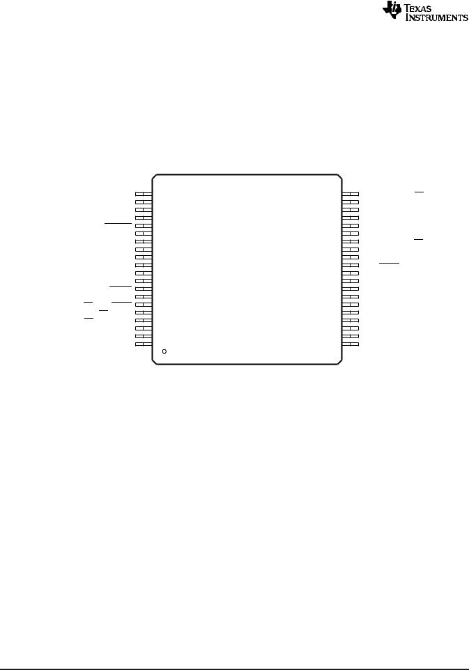
2.1Pin Assignments
Figure 2-1 shows the 64-pin PAG Thin Quad Flatpack (TQFP) pin assignments. Figure 2-2 shows the 80-pin PN Low-Profile Quad Flatpack (LQFP) pin assignments.
|
|
|
|
|
|
|
|
GPIO36/TMS |
GPIO35/TDI |
|
GPIO37/TDO |
|
GPIO38/TCK/XCLKIN |
|
GPIO19/XCLKIN/SPISTEA/LINRXA/ECAP1 |
V |
V |
X1 |
X2 |
GPIO6/EPWM4A/EPWMSYNCI/EPWMSYNCO |
GPIO7/EPWM4B/SCIRXDA |
|
GPIO12/TZ1/SCITXDA |
|
GPIO16/SPISIMOA/TZ2 |
|
GPIO8/EPWM5A/ADCSOCAO |
|
GPIO17/SPISOMIA/TZ3 |
GPIO18/SPICLKA/LINTXA/XCLKOUT |
|
|
|
|
|||||||||||||||||||||||||||
|
|
|
|
|
|
|
|
|
|
|
|
|
|
|
|
|
|
|
|||||||||||||||||||||||||||||||||||||||||||
|
|
|
|
|
|
|
|
|
|
|
|
|
|
|
|
|
|
||||||||||||||||||||||||||||||||||||||||||||
|
|
|
|
|
|
|
|
|
|
|
|
|
|
|
|
|
|
||||||||||||||||||||||||||||||||||||||||||||
|
|
|
|
|
|
|
|
|
|
|
|
|
|
|
|
|
|
||||||||||||||||||||||||||||||||||||||||||||
|
|
|
|
|
|
|
|
|
|
|
|
|
|
|
|
|
|
||||||||||||||||||||||||||||||||||||||||||||
|
|
|
|
|
|
|
|
|
|
|
|
|
|
|
|
||||||||||||||||||||||||||||||||||||||||||||||
|
|
|
|
|
|
|
|
|
|
|
|
|
|
|
|
||||||||||||||||||||||||||||||||||||||||||||||
|
|
|
|
|
|
|
|
|
|
|
|
|
|
|
|
|
|
|
|
|
|
|
|
DD |
|
SS |
|
|
|
|
|
|
|
|
|
|
|
|
|
|
|
|
|
|
|
|
|
|
|
|
|
|
|
|
|
|
|
|
|
|
|
|
|
|
|
|
|
|
|
|
|
|
|
|
|
|
|
|
|
|
|
|
|
|
|
|
|
|
|
|
|
|
|
|
|
|
|
|
|
|
|
|
|
|
|
|
|
|
|
|
|
|
|
|
|
|
|
|
|
|
|
|
|
|
|
|
|
|
|
|
|
|
|
|
|
|
|
|
|
|
|
|
|
|
|
|
|
|
|
|
|
|
|
|
|
|
|
|
|
|
|
|
|
|
|
|
|
|
|
|
|
|
|
|
|
|
|
|
|
|
|
|
|
|
|
|
|
|
|
|
|
|
|
|
|
|
|
|
|
|
|
|
|
|
|
|
|
|
|
|
|
|
|
|
|
|
|
|
|
|
|
|
|
|
|
|
|
|
|
|
|
|
|
|
|
|
|
|
|
|
|
|
|
|
|
|
|
|
|
|
|
|
48 |
|
47 |
|
46 |
|
45 |
|
44 |
|
43 |
|
42 |
41 |
|
40 |
39 |
38 |
37 |
36 |
|
35 |
|
34 |
|
33 |
|
|
|
|
|
|
|
|
|||||||||||||||||||||||
GPIO11/EPWM6B/LINRXA |
|
|
|
49 |
|
|
|
|
|
|
|
|
|
|
|
|
|
|
|
|
|
|
|
|
|
|
|
|
|
|
|
|
|
|
|
|
|
|
|
|
|
|
|
|
|
|
|
32 |
|
|
|
|
|
|
|
||||||
|
|
|
|
|
|
|
|
|
|
|
|
|
|
|
|
|
|
|
|
|
|
|
|
|
|
|
|
|
|
|
|
|
|
|
|
|
|
|
|
|
|
|
|
|
|
|
|
|
GPIO28/SCIRXDA/SDAA/TZ2 |
||||||||||||
GPIO5/EPWM3B/SPSIMOA/ECAP1 |
|
50 |
|
|
|
|
|
|
|
|
|
|
|
|
|
|
|
|
|
|
|
|
|
|
|
|
|
|
|
|
|
|
|
|
|
|
|
|
|
|
|
|
|
|
|
31 |
|
|
|
GPIO9/EPWM5B/LINTXA |
|||||||||||
GPIO4/EPWM3A |
|
51 |
|
|
|
|
|
|
|
|
|
|
|
|
|
|
|
|
|
|
|
|
|
|
|
|
|
|
|
|
|
|
|
|
|
|
|
|
|
|
|
|
|
|
|
30 |
|
|
|
TEST2 |
|||||||||||
|
|
|
|
|
|
52 |
|
|
|
|
|
|
|
|
|
|
|
|
|
|
|
|
|
|
|
|
|
|
|
|
|
|
|
|
|
|
|
|
|
|
|
|
|
|
|
|
|
|
|
29 |
|
|
|
VDDIO |
|||||||
GPIO10/EPWM6A/ADCSOCBO |
|
|
|
|
|
|
|
|
|
|
|
|
|
|
|
|
|
|
|
|
|
|
|
|
|
|
|
|
|
|
|
|
|
|
|
|
|
|
|
|
|
|
|
|
|
|
|
|
|
||||||||||||
GPIO3/EPWM2B/SPISOMIA/COMP2OUT |
|
53 |
|
|
|
|
|
|
|
|
|
|
|
|
|
|
|
|
|
|
|
|
|
|
|
|
|
|
|
|
|
|
|
|
|
|
|
|
|
|
|
|
|
|
|
28 |
|
|
|
VSS |
|||||||||||
GPIO2/EPWM2A |
|
54 |
|
|
|
|
|
|
|
|
|
|
|
|
|
|
|
|
|
|
|
|
|
|
|
|
|
|
|
|
|
|
|
|
|
|
|
|
|
|
|
|
|
|
|
27 |
|
|
|
|
|
|
|
||||||||
|
|
|
|
|
|
|
|
|
|
|
|
|
|
|
|
|
|
|
|
|
|
|
|
|
|
|
|
|
|
|
|
|
|
|
|
|
|
|
|
|
|
|
|
|
|
|
|
|
GPIO29/SCITXDA/SCLA/TZ3 |
||||||||||||
GPIO1/EPWM1B/COMP1OUT |
|
55 |
|
|
|
|
|
|
|
|
|
|
|
|
|
|
|
|
|
|
|
|
|
|
|
|
|
|
|
|
|
|
|
|
|
|
|
|
|
|
|
|
|
|
|
26 |
|
|
|
GPIO30/CANRXA |
|||||||||||
GPIO0/EPWM1A |
|
56 |
|
|
|
|
|
|
|
|
|
|
|
|
|
|
|
|
|
|
|
|
|
|
|
|
|
|
|
|
|
|
|
|
|
|
|
|
|
|
|
|
|
|
|
25 |
|
|
|
GPIO31/CANTXA |
|||||||||||
|
|
VDDIO |
|
57 |
|
|
|
|
|
|
|
|
|
|
|
|
|
|
|
|
|
|
|
|
|
|
|
|
|
|
|
|
|
|
|
|
|
|
|
|
|
|
|
|
|
|
|
24 |
|
|
|
ADCINB7 |
|||||||||
|
|
VSS |
|
58 |
|
|
|
|
|
|
|
|
|
|
|
|
|
|
|
|
|
|
|
|
|
|
|
|
|
|
|
|
|
|
|
|
|
|
|
|
|
|
|
|
|
|
|
23 |
|
|
|
ADCINB6/COMP3B/AIO14 |
|||||||||
|
|
VDD |
|
59 |
|
|
|
|
|
|
|
|
|
|
|
|
|
|
|
|
|
|
|
|
|
|
|
|
|
|
|
|
|
|
|
|
|
|
|
|
|
|
|
|
|
|
|
22 |
|
|
|
ADCINB4/COMP2B/AIO12 |
|||||||||
|
|
|
|
|
|
|
|
|
|
|
|
|
|
|
|
|
|
|
|
|
|
|
|
|
|
|
|
|
|
|
|
|
|
|
|
|
|
|
|
|
|
|
|
|
|
|
|
|
|
|
|
|
|
||||||||
|
|
VREGENZ |
|
|
|
60 |
|
|
|
|
|
|
|
|
|
|
|
|
|
|
|
|
|
|
|
|
|
|
|
|
|
|
|
|
|
|
|
|
|
|
|
|
|
|
|
|
|
|
|
21 |
|
|
|
ADCINB3 |
|||||||
GPIO34/COMP2OUT/COMP3OUT |
|
61 |
|
|
|
|
|
|
|
|
|
|
|
|
|
|
|
|
|
|
|
|
|
|
|
|
|
|
|
|
|
|
|
|
|
|
|
|
|
|
|
|
|
|
|
20 |
|
|
|
ADCINB2/COMP1B/AIO10 |
|||||||||||
GPIO20/EQEP1A/COMP1OUT |
|
62 |
|
|
|
|
|
|
|
|
|
|
|
|
|
|
|
|
|
|
|
|
|
|
|
|
|
|
|
|
|
|
|
|
|
|
|
|
|
|
|
|
|
|
|
19 |
|
|
|
ADCINB1 |
|||||||||||
GPIO21/EQEP1B/COMP2OUT |
|
63 |
|
|
|
|
|
|
|
|
|
|
|
|
|
|
|
|
|
|
|
|
|
|
|
|
|
|
|
|
|
|
|
|
|
|
|
|
|
|
|
|
|
|
|
18 |
|
|
|
ADCINB0 |
|||||||||||
GPIO24/ECAP1 |
|
64 |
|
|
|
|
|
|
|
|
|
|
|
|
|
|
|
|
|
|
|
|
|
|
|
|
|
|
|
|
|
|
|
|
|
|
|
|
|
|
|
|
|
|
|
17 |
|
|
|
VSSA/VREFLO |
|||||||||||
|
|
|
|
|
1 |
|
2 |
3 |
4 |
5 |
6 |
|
7 |
8 |
|
9 |
|
10 |
|
11 |
|
12 |
|
13 |
|
14 |
|
15 |
|
16 |
|
|
|
|
|
|
|
|
|||||||||||||||||||||||
|
|
|
|
|
|
|
|
|
|
|
|
|
|
|
|
|
|
|
|
|
|
|
|
|
|
|
|
|
|
|
|
|
|
|
|
|
|
|
|
|
|
|
|
||||||||||||||||||
|
|
|
|
|
|
|
|
|
|
|
|
|
|
|
|
|
|
|
|
|
|
|
|
|
|
|
|
|
|
|
|
|
|
|
|
|
|
|
|
|
|
|
|
|
|
|
|
|
|
|
|
|
|
|
|
|
|
|
|
|
|
|
|
|
|
|
|
|
|
|
|
|
|
|
|
|
|
|
|
|
|
|
|
|
|
|
|
|
|
|
|
|
|
|
|
|
|
|
|
|
|
|
|
|
|
|
|
|
|
|
|
|
|
|
|
|
|
|
|
|
|
|
|
|
|
|
|
|
|
|
|
|
GPIO22/EQEP1S/LINTXA |
|
GPIO32/SDAA/EPWMSYNCI/ADCSOCAO |
|
GPIO33/SCLA/EPWMSYNCO/ADCSOCBO |
|
GPIO23/EQEP1I/LINRXA |
|
V |
|
V |
|
XRS |
|
TRST |
|
ADCINA7 |
|
ADCINA6/COMP3A/AIO6 |
|
ADCINA4/COMP2A/AIO4 |
|
ADCINA3 |
|
ADCINA2/COMP1A/AIO2 |
|
ADCINA1 |
|
ADCINA0/VREFHI |
|
V |
|
|
|
|
||||||||||||||||||
|
|
|
|
|
|
|
|
|
|
|
|
|
|
|
|
|
|
|
|
|
DD |
|
SS |
|
|
|
|
|
|
|
|
|
|
|
|
|
|
|
|
|
|
|
|
|
|
|
|
|
|
|
DDA |
|
|
|
|
||||||
|
|
|
|
|
|
|
|
|
|
|
|
|
|
|
|
|
|
|
|
|
|
|
|
|
|
|
|
|
|
|
|
|
|
|
|
|
|
|
|
|
|
|
|
|
|
|
|
|
|
|
|
|
|
|
|
|
|
|
|
|
|
A.Pin 15: VREFHI and ADCINA0 share the same pin on the 64-pin PAG device and their use is mutually exclusive to one another.
B.Pin 17: VREFLO is always connected to VSSA on the 64-pin PAG device.
Figure 2-1. 2803x 64-Pin PAG TQFP (Top View)
Copyright © 2009–2010, Texas Instruments Incorporated |
Introduction |
5 |
Submit Documentation Feedback
Product Folder Link(s): TMS320F28030 TMS320F28031 TMS320F28032 TMS320F28033 TMS320F28034
TMS320F28035
TMS320F28030, TMS320F28031, TMS320F28032
TMS320F28033, TMS320F28034, TMS320F28035
SPRS584D–APRIL 2009 –REVISED JUNE 2010 |
www.ti.com |
GPIO11/EPWM6B/LINRXA
GPIO5/EPWM3B/SPISIMOA/ECAP1
GPIO4/EPWM3A
GPIO40/EPWM7A
GPIO10/EPWM6A/ADCSOCBO
GPIO3/EPWM2B/SPISOMIA/COMP2OUT
GPIO2/EPWM2A
GPIO1/EPWM1B/COMP1OUT
GPIO0/EPWM1A
VDDIO
VSS
VDD
VREGENZ
GPIO34/COMP2OUT/COMP3OUT
GPIO15/TZ1/LINRXA/SPISTEB
GPIO13/TZ2/SPISOMIB
GPIO14/TZ3/LINTXA/SPICLKB
GPIO20/EQEP1A/COMP1OUT
GPIO21/EQEP1B/COMP2OUT
GPIO24/ECAP1/SPISIMOB
61
62
63
64
65
66
67
68
69
70
71
72
73
74
75
76
77
78
79
80
GPIO36/TMS |
GPIO35/TDI |
|
GPIO37/TDO |
GPIO38/TCK/XCLKIN |
GPIO39 |
|
GPIO19/XCLKIN/SPISTEA/LINRXA/ECAP1 |
V |
V |
X1 |
|
X2 |
GPIO6/EPWM4A/EPWMSYNCI/EPWMSYNCO |
GPIO7/EPWM4B/SCIRXDA |
|
GPIO41/EPWM7B |
|
GPIO12/TZ1/SCITXDA/SPISIMOB |
|
GPIO16/SPISIMOA/TZ2 |
GPIO44 |
|
GPIO25/SPISOMIB |
|
GPIO8/EPWM5A/ADCSOCAO |
|
GPIO17/SPISOMIA/TZ3 |
|
GPIO18/SPICLKA/LINTXA/XCLKOUT |
|||||||||||||
|
|
|
|
|
|
|
|
|
|
|||||||||||||||||||||||||||||||||
|
|
|
|
|
|
|
|
|||||||||||||||||||||||||||||||||||
|
|
|
|
|
|
|
|
|
|
|||||||||||||||||||||||||||||||||
|
|
|
|
|
|
|
|
|
|
|||||||||||||||||||||||||||||||||
|
|
|
|
|
|
|
|
|
||||||||||||||||||||||||||||||||||
|
|
|
|
|
|
|
||||||||||||||||||||||||||||||||||||
|
|
|
|
|
|
|
||||||||||||||||||||||||||||||||||||
|
|
|
|
|
|
|
|
|
|
|
|
DD |
SS |
|
|
|
|
|
|
|
|
|
|
|
|
|
|
|
|
|
|
|
|
|
|
|
|
|
|
|
||
|
|
|
|
|
|
|
|
|
|
|
|
|
|
|
|
|
|
|
|
|
|
|
|
|
|
|
|
|
|
|
|
|
|
|
|
|
|
|
|
|
|
|
|
|
|
|
|
|
|
|
|
|
|
|
|
|
|
|
|
|
|
|
|
|
|
|
|
|
|
|
|
|
|
|
|
|
|
|
|
|
|
|
|
|
|
|
|
|
|
|
|
|
|
|
|
|
|
|
|
|
|
|
|
|
|
|
|
|
|
|
|
|
|
|
|
|
|
|
|
|
|
|
|
|
|
|
|
|
60 |
|
59 |
58 |
|
57 |
|
56 |
55 |
|
54 |
|
53 |
|
52 |
51 |
|
50 |
|
49 |
48 |
|
|
47 |
|
|
46 |
|
45 |
44 |
|
|
43 |
|
|
42 |
41 |
||||||
1 |
|
|
2 |
3 |
|
4 |
|
5 |
6 |
|
7 |
|
8 |
|
9 |
10 |
|
11 |
|
12 |
13 |
|
14 |
|
15 |
|
16 |
17 |
|
18 |
|
19 |
|
20 |
|||||
|
|
|
|
|
|
|
|
|
|
|
|
|
|
|
|
|
|
|
|
|
|
|
|
|
|
|
|
|
|
|
|
|
|
|
|
|
|
|
|
|
|
|
|
|
|
|
|
|
|
|
|
|
|
|
|
|
|
|
|
|
|
|
|
|
|
|
|
|
|
|
|
|
|
|
|
|
|
|
|
|
|
|
|
|
|
|
|
|
|
|
|
|
|
|
|
|
|
|
|
|
|
|
|
|
|
|
|
|
|
|
|
|
|
|
|
|
|
|
|
GPIO22/EQEP1S/LINTXA |
|
|
|
|
|
GPIO23/EQEP1I/LINRXA |
GPIO42/COMP1OUT |
|
|
|
DD |
|
XRS |
|
TRST |
ADCINA7 |
|
|
|
|
|
|
|
|
|
|
ADCINA1 |
|
|
REFHI |
DDA |
||||||||
|
GPIO32/SDAA/EPWMSYNCI/ADCSOCAO |
|
GPIO33/SCLA/EPWMSYNCO/ADCSOCBO |
|
GPIO43/COMP2OUT |
SS |
|
ADCINA6/COMP3A/AIO6 |
|
ADCINA5 |
ADCINA4/COMP2A/AIO4 |
ADCINA3 |
ADCINA2/COMP1A/AIO2 |
|
ADCINA0 |
||||||||||||||||||||||||
|
|
|
V |
V |
|
|
|
V |
V |
||||||||||||||||||||||||||||||
|
|
|
|
|
|
|
|
|
|
|
|
|
|
|
|
|
|
|
|
|
|
|
|
|
|
||||||||||||||
40
39
38
37
36
35
34
33
32
31
30
29
28
27
26
25
24
23
22
21
GPIO28/SCIRXDA/SDAA/TZ2
GPIO9/EPWM5B/LINTXA
TEST2
GPIO26/SPICLKB
VDDIO
VSS
GPIO29/SCITXDA/SCLA/TZ3
GPIO30/CANRXA
GPIO31/CANTXA
GPIO27/SPISTEB
ADCINB7
ADCINB6/COMP3B/AIO14
ADCINB5
ADCINB4/COMP2B/AIO12
ADCINB3
ADCINB2/COMP1B/AIO10
ADCINB1
ADCINB0
VREFLO
VSSA
Figure 2-2. 2803x 80-Pin PN LQFP (Top View)
6 |
Introduction |
Copyright © 2009–2010, Texas Instruments Incorporated |
Submit Documentation Feedback
Product Folder Link(s): TMS320F28030 TMS320F28031 TMS320F28032 TMS320F28033 TMS320F28034
TMS320F28035

TMS320F28030, TMS320F28031, TMS320F28032
TMS320F28033, TMS320F28034, TMS320F28035
www.ti.com |
SPRS584D –APRIL 2009 –REVISED JUNE 2010 |
2.2Signal Descriptions
Table 2-2 describes the signals. With the exception of the JTAG pins, the GPIO function is the default at reset, unless otherwise mentioned. The peripheral signals that are listed under them are alternate functions. Some peripheral functions may not be available in all devices. See Table 2-1 for details. Inputs are not 5-V tolerant. All GPIO pins are I/O/Z and have an internal pullup, which can be selectively enabled/disabled on a per-pin basis. This feature only applies to the GPIO pins. The pullups on the PWM pins are not enabled at reset. The pullups on other GPIO pins are enabled upon reset. The AIO pins do not have an internal pullup.
|
|
|
|
|
|
|
Table 2-2. Terminal Functions(1) |
|||
|
|
|
TERMINAL |
|
|
|
|
|
|
|
|
|
|
|
|
|
I/O/Z |
|
DESCRIPTION |
||
|
NAME |
|
PN |
PAG |
|
|||||
|
|
PIN # |
PIN # |
|
|
|
|
|
||
|
|
|
|
|
|
|
|
|
||
|
|
|
|
|
|
|
|
JTAG |
||
|
|
|
|
|
|
|
|
|
|
|
|
|
|
|
|
|
|
|
JTAG test reset with internal pulldown. |
TRST, |
when driven high, gives the scan |
|
|
|
|
|
|
|
|
system control of the operations of the device. If this signal is not connected or driven |
||
|
|
|
|
|
|
|
|
low, the device operates in its functional mode, and the test reset signals are ignored. |
||
|
|
|
|
|
|
|
|
NOTE: TRST is an active high test pin and must be maintained low at all times during |
||
|
TRST |
|
|
10 |
8 |
I |
|
normal device operation. An external pull-down resistor is required on this pin. The |
||
|
|
|
|
|
|
|
|
value of this resistor should be based on drive strength of the debugger pods |
||
|
|
|
|
|
|
|
|
applicable to the design. A 2.2-kΩ resistor generally offers adequate protection. Since |
||
|
|
|
|
|
|
|
|
this is application-specific, it is recommended that each target board be validated for |
||
|
|
|
|
|
|
|
|
proper operation of the debugger and the application. (↓) |
||
|
TCK |
|
See GPIO38 |
I |
|
See GPIO38. JTAG test clock with internal pullup (↑) |
||||
|
TMS |
|
See GPIO36 |
I |
|
See GPIO36. JTAG test-mode select (TMS) with internal pullup. This serial control |
||||
|
|
|
input is clocked into the TAP controller on the rising edge of TCK. (↑) |
|||||||
|
|
|
|
|
|
|
|
|||
|
TDI |
|
See GPIO35 |
I |
|
See GPIO35. JTAG test data input (TDI) with internal pullup. TDI is clocked into the |
||||
|
|
|
selected register (instruction or data) on a rising edge of TCK. (↑) |
|||||||
|
|
|
|
|
|
|
|
|||
|
|
|
|
|
|
|
|
See GPIO37. JTAG scan out, test data output (TDO). The contents of the selected |
||
|
TDO |
|
See GPIO37 |
O/Z |
|
register (instruction or data) are shifted out of TDO on the falling edge of TCK. (8 mA |
||||
|
|
|
|
|
|
|
|
drive) |
||
|
|
|
|
|
|
|
|
|
|
|
|
|
|
|
|
|
|
|
FLASH |
||
|
|
|
|
|
|
|
|
|
|
|
|
TEST2 |
|
38 |
30 |
I/O |
|
Test Pin. Reserved for TI. Must be left unconnected. |
|||
|
|
|
|
|
|
|
|
|
|
|
|
|
|
|
|
|
|
|
CLOCK |
||
|
|
|
|
|
|
|
|
|
|
|
|
|
|
|
|
|
|
|
See GPIO18. Output clock derived from SYSCLKOUT. XCLKOUT is either the same |
||
|
|
|
|
|
|
|
|
frequency, one-half the frequency, or one-fourth the frequency of SYSCLKOUT. This |
||
|
XCLKOUT |
|
See GPIO18 |
O/Z |
|
is controlled by bits 1:0 (XCLKOUTDIV) in the XCLK register. At reset, XCLKOUT = |
||||
|
|
|
SYSCLKOUT/4. The XCLKOUT signal can be turned off by setting XCLKOUTDIV |
|||||||
|
|
|
|
|
|
|
|
|||
|
|
|
|
|
|
|
|
to 3. The mux control for GPIO18 must also be set to XCLKOUT for this signal to |
||
|
|
|
|
|
|
|
|
propogate to the pin. |
||
|
|
|
|
|
|
|
|
|
|
|
|
|
|
|
|
|
|
|
See GPIO19 and GPIO38. External oscillator input. Pin source for the clock is |
||
|
|
|
|
|
|
|
|
controlled by the XCLKINSEL bit in the XCLK register, GPIO38 is the default |
||
|
|
|
|
|
|
|
|
selection. This pin feeds a clock from an external 3.3-V oscillator. In this case, the X1 |
||
|
|
|
|
|
|
|
|
pin, if available, must be tied to GND and the on-chip crystal oscillator must be |
||
|
|
|
|
See GPIO19 and |
|
|
disabled via bit 14 in the CLKCTL register. If a crystal/resonator is used, the XCLKIN |
|||
|
XCLKIN |
|
I |
|
path must be disabled by bit 13 in the CLKCTL register. |
|||||
|
|
GPIO38 |
|
|||||||
|
|
|
|
|
|
NOTE: Designs that use the GPIO38/TCK/XCLKIN pin to supply an external clock for |
||||
|
|
|
|
|
|
|
|
|||
|
|
|
|
|
|
|
|
normal device operation may need to incorporate some hooks to disable this path |
||
|
|
|
|
|
|
|
|
during debug using the JTAG connector. This is to prevent contention with the TCK |
||
|
|
|
|
|
|
|
|
signal, which is active during JTAG debug sessions. The zero-pin internal oscillators |
||
|
|
|
|
|
|
|
|
may be used during this time to clock the device. |
||
|
|
|
|
|
|
|
|
|
|
|
|
|
|
|
|
|
|
|
On-chip crystal-oscillator input. To use this oscillator, a quartz crystal or a ceramic |
||
|
X1 |
|
52 |
41 |
I |
|
resonator must be connected across X1 and X2. In this case, the XCLKIN path must |
|||
|
|
|
be disabled by bit 13 in the CLKCTL register. If this pin is not used, it must be tied to |
|||||||
|
|
|
|
|
|
|
|
|||
|
|
|
|
|
|
|
|
GND. (I) |
||
|
|
|
|
|
|
|
|
|
|
|
|
X2 |
|
51 |
40 |
O |
|
On-chip crystal-oscillator output. A quartz crystal or a ceramic resonator must be |
|||
|
|
|
connected across X1 and X2. If X2 is not used, it must be left unconnected. (O) |
|||||||
|
|
|
|
|
|
|
|
|||
|
|
|
|
|
|
|
|
|
|
|
(1)I = Input, O = Output, Z = High Impedance, OD = Open Drain, ↑ = Pullup, ↓ = Pulldown
Copyright © 2009–2010, Texas Instruments Incorporated |
Introduction |
7 |
Submit Documentation Feedback
Product Folder Link(s): TMS320F28030 TMS320F28031 TMS320F28032 TMS320F28033 TMS320F28034
TMS320F28035

TMS320F28030, TMS320F28031, TMS320F28032
TMS320F28033, TMS320F28034, TMS320F28035
SPRS584D–APRIL 2009 –REVISED JUNE 2010 www.ti.com
Table 2-2. Terminal Functions (1) (continued)
|
|
|
TERMINAL |
|
|
|
|
|
|
|
|
|
|
|
|
|
I/O/Z |
|
|
DESCRIPTION |
|
|
NAME |
|
PN |
PAG |
|
|
||||
|
|
PIN # |
PIN # |
|
|
|
|
|
||
|
|
|
|
|
|
|
|
|
||
|
|
|
|
|
|
|
|
|
||
|
|
|
|
|
|
|
|
RESET |
||
|
|
|
|
|
|
|
|
|
|
|
|
|
|
|
|
|
|
|
Device Reset (in) and Watchdog Reset (out). Piccolo devices have a built-in |
||
|
|
|
|
|
|
|
|
power-on-reset (POR) and brown-out-reset (BOR) circuitry. As such, no external |
||
|
|
|
|
|
|
|
|
circuitry is needed to generate a reset pulse. During a power-on or brown-out |
||
|
|
|
|
|
|
|
|
condition, this pin is driven low by the device. See the electrical section for thresholds |
||
|
|
|
|
|
|
|
|
of the POR/BOR block. This pin is also driven low by the MCU when a watchdog reset |
||
|
|
|
|
|
|
|
|
occurs. During watchdog reset, the |
XRS |
pin is driven low for the watchdog reset |
|
|
|
|
|
|
|
|
duration of 512 OSCCLK cycles. If need be, an external circuitry may also drive this |
||
|
XRS |
|
9 |
7 |
I/O |
|
||||
|
|
|
pin to assert a device reset. In this case, it is recommended that this pin be driven by |
|||||||
|
|
|
|
|
|
|
|
|||
|
|
|
|
|
|
|
|
an open-drain device. An R-C circuit must be connected to this pin for noise immunity |
||
|
|
|
|
|
|
|
|
reasons. Regardless of the source, a device reset causes the device to terminate |
||
|
|
|
|
|
|
|
|
execution. The program counter points to the address contained at the location |
||
|
|
|
|
|
|
|
|
0x3FFFC0. When reset is deactivated, execution begins at the location designated by |
||
|
|
|
|
|
|
|
|
the program counter. The output buffer of this pin is an open-drain with an internal |
||
|
|
|
|
|
|
|
|
pullup. (I/OD) |
||
|
|
|
|
|
|
|
|
|
|
|
|
|
|
|
|
|
|
ADC, COMPARATOR, ANALOG I/O |
|||
|
|
|
|
|
|
|
|
|
|
|
|
ADCINA7 |
|
11 |
9 |
I |
|
ADC Group A, Channel 7 input |
|||
|
|
|
|
|
|
|
|
|
|
|
|
ADCINA6 |
|
|
|
I |
|
ADC Group A, Channel 6 input |
|||
|
COMP3A |
|
12 |
10 |
|
Comparator Input 3A |
||||
|
|
I/O |
|
|||||||
|
AIO6 |
|
|
|
|
Digital AIO 6 |
||||
|
|
|
|
|
|
|||||
|
|
|
|
|
|
|
|
|
|
|
|
ADCINA5 |
|
13 |
– |
|
|
|
|
|
|
|
|
|
|
|
|
|
|
|
|
|
|
ADCINA4 |
|
|
|
I |
|
ADC Group A, Channel 4 input |
|||
|
COMP2A |
|
14 |
11 |
I |
|
Comparator Input 2A |
|||
|
AIO4 |
|
|
|
I/O |
|
Digital AIO 4 |
|||
|
|
|
|
|
|
|
|
|
|
|
|
ADCINA3 |
|
15 |
12 |
I |
|
ADC Group A, Channel 3 input |
|||
|
|
|
|
|
|
|
|
|
|
|
|
ADCINA2 |
|
|
|
I |
|
ADC Group A, Channel 2 input |
|||
|
COMP1A |
|
16 |
13 |
I |
|
Comparator Input 1A |
|||
|
AIO2 |
|
|
|
I/O |
|
Digital AIO 2 |
|||
|
ADCINA1 |
|
17 |
14 |
I |
|
ADC Group A, Channel 1 input |
|||
|
|
|
|
|
|
|
|
|
|
|
|
|
|
|
|
|
|
|
ADC Group A, Channel 0 input. |
||
|
ADCINA0 |
|
18 |
15 |
I |
|
NOTE: VREFHI and ADCINA0 share the same pin on the 64-pin PAG device and their |
|||
|
|
|
|
|
|
|
|
use is mutually exclusive to one another. |
||
|
|
|
|
|
|
|
|
|
|
|
|
|
|
|
|
|
|
|
ADC External Reference – only used when in ADC external reference mode. See |
||
|
VREFHI |
|
19 |
15 |
|
|
ADC Section.. |
|||
|
|
|
|
NOTE: VREFHI and ADCINA0 share the same pin on the 64-pin PAG device and their |
||||||
|
|
|
|
|
|
|
|
|||
|
|
|
|
|
|
|
|
use is mutually exclusive to one another. |
||
|
|
|
|
|
|
|
|
|
|
|
|
ADCINB7 |
|
30 |
24 |
I |
|
ADC Group B, Channel 7 input |
|||
|
|
|
|
|
|
|
|
|
|
|
|
ADCINB6 |
|
|
|
I |
|
ADC Group B, Channel 6 input |
|||
|
COMP3B |
|
29 |
23 |
|
Comparator Input 3B |
||||
|
|
I/O |
|
|||||||
|
AIO14 |
|
|
|
|
Digital AIO 14 |
||||
|
|
|
|
|
|
|||||
|
|
|
|
|
|
|
|
|
|
|
|
ADCINB5 |
|
28 |
– |
|
|
|
|
|
|
|
|
|
|
|
|
|
|
|
|
|
|
ADCINB4 |
|
|
|
I |
|
ADC Group B, Channel 4 input |
|||
|
COMP2B |
|
27 |
22 |
I |
|
Comparator Input 2B |
|||
|
AIO12 |
|
|
|
I/O |
|
Digital AIO12 |
|||
|
|
|
|
|
|
|
|
|
|
|
|
ADCINB3 |
|
26 |
21 |
I |
|
ADC Group B, Channel 3 input |
|||
|
|
|
|
|
|
|
|
|
|
|
|
ADCINB2 |
|
|
|
I |
|
ADC Group B, Channel 2 input |
|||
|
COMP1B |
|
25 |
20 |
I |
|
Comparator Input 1B |
|||
|
AIO10 |
|
|
|
I/O |
|
Digital AIO 10 |
|||
|
|
|
|
|
|
|
|
|
|
|
|
ADCINB1 |
|
24 |
19 |
I |
|
ADC Group B, Channel 1 input |
|||
|
|
|
|
|
|
|
|
|
|
|
|
ADCINB0 |
|
23 |
18 |
|
|
|
|
|
|
|
|
|
|
|
|
|
|
|
|
|
|
VREFLO |
|
22 |
17 |
|
|
NOTE: VREFLO is always connected to VSSA on the 64-pin PAG device. |
|||
8 |
Introduction |
Copyright © 2009–2010, Texas Instruments Incorporated |
Submit Documentation Feedback
Product Folder Link(s): TMS320F28030 TMS320F28031 TMS320F28032 TMS320F28033 TMS320F28034
TMS320F28035

|
TMS320F28030, TMS320F28031, TMS320F28032 |
|
TMS320F28033, TMS320F28034, TMS320F28035 |
www.ti.com |
SPRS584D –APRIL 2009 –REVISED JUNE 2010 |
Table 2-2. Terminal Functions (1) (continued)
|
|
|
TERMINAL |
|
|
|
|
|
|
|
|
|
|
|
I/O/Z |
|
DESCRIPTION |
|
NAME |
|
PN |
PAG |
|
|||
|
|
PIN # |
PIN # |
|
|
|
||
|
|
|
|
|
|
|
||
|
|
|
|
|
|
|
|
|
|
|
|
|
|
|
|
|
CPU AND I/O POWER |
|
|
|
|
|
|
|
||
|
VDDA |
|
20 |
16 |
|
|
Analog Power Pin. Tie with a 2.2-mF capacitor (typical) close to the pin. |
|
|
VSSA |
|
21 |
17 |
|
|
Analog Ground Pin. |
|
|
|
|
|
NOTE: VREFLO is always connected to VSSA on the 64-pin PAG device. |
||||
|
|
|
|
|
|
|
|
|
|
VDD |
|
7 |
5 |
|
|
CPU and Logic Digital Power Pins – no supply source needed when using internal |
|
|
VDD |
|
54 |
43 |
|
|
VREG. Tie with 1.2 µF (minimum) ceramic capacitor (10% tolerance) to ground when |
|
|
|
|
|
using internal VREG. Higher value capacitors may be used, but could impact |
||||
|
VDD |
|
72 |
59 |
|
|
||
|
|
|
|
supply-rail ramp-up time. |
||||
|
VDDIO |
|
36 |
29 |
|
|
Digital I/O and Flash Power Pin – Single Supply source when VREG is enabled |
|
|
VDDIO |
|
70 |
57 |
|
|
||
|
|
|
|
|
||||
|
VSS |
|
8 |
6 |
|
|
|
|
|
VSS |
|
35 |
28 |
|
|
Digital Ground Pins |
|
|
VSS |
|
53 |
42 |
|
|
||
|
|
|
|
|
||||
|
VSS |
|
71 |
58 |
|
|
|
|
|
|
|
|
|
|
VOLTAGE REGULATOR CONTROL SIGNAL |
||
|
|
|
|
|
|
|
|
|
|
VREGENZ |
|
|
73 |
60 |
I |
|
Internal VREG Enable/Disable – pull low to enable VREG, pull high to disable VREG |
|
|
|
|
|
|
|
GPIO AND PERIPHERAL SIGNALS (1) |
|
|
GPIO0 |
|
69 |
56 |
I/O/Z |
|
General purpose input/output 0 |
|
|
EPWM1A |
|
|
|
O |
|
Enhanced PWM1 Output A and HRPWM channel |
|
|
– |
|
|
|
– |
|
– |
|
|
– |
|
|
|
– |
|
– |
|
|
|
|
|
|
|
|
|
|
|
GPIO1 |
|
68 |
55 |
I/O/Z |
|
General purpose input/output 1 |
|
|
EPWM1B |
|
|
|
O |
|
Enhanced PWM1 Output B |
|
|
– |
|
|
|
|
|
– |
|
|
COMP1OUT |
|
|
|
O |
|
Direct output of Comparator 1 |
|
|
|
|
|
|
|
|
|
|
|
GPIO2 |
|
67 |
54 |
I/O/Z |
|
General purpose input/output 2 |
|
|
EPWM2A |
|
|
|
O |
|
Enhanced PWM2 Output A and HRPWM channel |
|
|
– |
|
|
|
|
|
– |
|
|
– |
|
|
|
|
|
– |
|
|
|
|
|
|
|
|
|
|
|
GPIO3 |
|
66 |
53 |
I/O/Z |
|
General purpose input/output 3 |
|
|
EPWM2B |
|
|
|
O |
|
Enhanced PWM2 Output B |
|
|
SPISOMIA |
|
|
|
I/O |
|
SPI-A slave out, master in |
|
|
COMP2OUT |
|
|
|
O |
|
Direct output of Comparator 2 |
|
|
|
|
|
|
|
|
|
|
|
GPIO4 |
|
63 |
51 |
I/O/Z |
|
General purpose input/output 4 |
|
|
EPWM3A |
|
|
|
O |
|
Enhanced PWM3 output A and HRPWM channel |
|
|
– |
|
|
|
|
|
– |
|
|
– |
|
|
|
|
|
– |
|
|
|
|
|
|
|
|
|
|
|
GPIO5 |
|
62 |
50 |
I/O/Z |
|
General purpose input/output 5 |
|
|
EPWM3B |
|
|
|
O |
|
Enhanced PWM3 output B |
|
|
SPISIMOA |
|
|
|
I/O |
|
SPI-A slave in, master out |
|
|
ECAP1 |
|
|
|
I/O |
|
Enhanced Capture input/output 1 |
|
|
|
|
|
|
|
|
|
|
(1)The GPIO function (shown in bold italics) is the default at reset. The peripheral signals that are listed under them are alternate functions. For JTAG pins that have the GPIO functionality multiplexed, the input path to the GPIO block is always valid. The output path from the GPIO block and the path to the JTAG block from a pin is enabled/disabled based on the condition of the TRST signal. See the
TMS320x2803x Piccolo System Control and Interrupts Reference Guide (literature number SPRUGL8) for details.
Copyright © 2009–2010, Texas Instruments Incorporated |
Introduction |
9 |
Submit Documentation Feedback
Product Folder Link(s): TMS320F28030 TMS320F28031 TMS320F28032 TMS320F28033 TMS320F28034
TMS320F28035

TMS320F28030, TMS320F28031, TMS320F28032
TMS320F28033, TMS320F28034, TMS320F28035
SPRS584D–APRIL 2009 –REVISED JUNE 2010 www.ti.com
Table 2-2. Terminal Functions (1) (continued)
|
|
|
|
TERMINAL |
|
|
|
|
|
|
|
|
|
|
|
I/O/Z |
DESCRIPTION |
|
|
NAME |
PN |
PAG |
||||
|
|
PIN # |
PIN # |
|
|
|||
|
|
|
|
|
|
|
||
|
|
|
|
|
|
|||
|
GPIO6 |
50 |
39 |
I/O/Z |
General purpose input/output 6 |
|||
|
EPWM4A |
|
|
O |
Enhanced PWM4 output A and HRPWM channel |
|||
|
EPWMSYNCI |
|
|
I |
External ePWM sync pulse input |
|||
|
EPWMSYNCO |
|
|
O |
External ePWM sync pulse output |
|||
|
|
|
|
|
|
|||
|
GPIO7 |
49 |
38 |
I/O/Z |
General purpose input/output 7 |
|||
|
EPWM4B |
|
|
O |
Enhanced PWM4 output B |
|||
|
SCIRXDA |
|
|
I |
SCI-A receive data |
|||
|
– |
|
|
|
– |
|||
|
|
|
|
|
|
|||
|
GPIO8 |
43 |
35 |
I/O/Z |
General purpose input/output 8 |
|||
|
EPWM5A |
|
|
O |
Enhanced PWM5 output A and HRPWM channel |
|||
|
– |
|
|
|
– |
|||
|
|
|
|
|
O |
ADC start-of-conversion A |
||
|
ADCSOCAO |
|
|
|||||
|
GPIO9 |
39 |
31 |
I/O/Z |
General purpose input/output 9 |
|||
|
EPMW5B |
|
|
O |
Enhanced PWM5 output B |
|||
|
LINTXA |
|
|
|
LIN transmit A |
|||
|
– |
|
|
|
– |
|||
|
|
|
|
|
|
|||
|
GPIO10 |
65 |
52 |
I/O/Z |
General purpose input/output 10 |
|||
|
EPWM6A |
|
|
O |
Enhanced PWM6 output A and HRPWM channel |
|||
|
– |
|
|
|
– |
|||
|
|
|
|
|
O |
ADC start-of-conversion B |
||
|
ADCSOCBO |
|
|
|||||
|
GPIO11 |
61 |
49 |
I/O/Z |
General purpose input/output 11 |
|||
|
EPWM6B |
|
|
|
Enhanced PWM6 output B |
|||
|
LINRXA |
|
|
|
LIN receive A |
|||
|
– |
|
|
|
– |
|||
|
|
|
|
|
|
|
||
|
GPIO12 |
47 |
37 |
I/O/Z |
General purpose input/output 12 |
|||
|
|
|
|
|
|
I |
Trip Zone input 1 |
|
|
TZ1 |
|
|
|||||
|
SCITXDA |
|
|
O |
SCI-A transmit data |
|||
|
SPISIMOB |
|
|
I/O |
SPI-B slave in, master out. |
|||
|
|
|
|
|
|
|
|
NOTE: The SPI-B peripheral is only available in the PN package. |
|
|
|
|
|
|
|
||
|
GPIO13 |
76 |
– |
I/O/Z |
General purpose input/output 13 |
|||
|
|
|
|
|
|
I |
Trip Zone input 2 |
|
|
TZ2 |
|
|
|||||
|
SPISOMIB |
|
|
I/O |
SPI-B slave out, master in |
|||
|
– |
|
|
|
– |
|||
|
|
|
|
|
|
|
||
|
GPIO14 |
77 |
– |
I/O/Z |
General purpose input/output 14 |
|||
|
|
|
|
|
|
I |
Trip zone input 3 |
|
|
TZ3 |
|
|
|||||
|
LINTXA |
|
|
O |
LIN transmit |
|||
|
SPICLKB |
|
|
I/O |
SPI-B clock input/output |
|||
|
|
|
|
|
|
|
||
|
GPIO15 |
75 |
– |
I/O/Z |
General purpose input/output 15 |
|||
|
|
|
|
|
|
I |
Trip zone input 1 |
|
|
TZ1 |
|
|
|||||
|
LINRXA |
|
|
I |
LIN receive |
|||
|
|
|
|
|
|
|
I/O |
SPI-B slave transmit enable input/output |
|
SPISTEB |
|
|
|||||
10 |
Introduction |
Copyright © 2009–2010, Texas Instruments Incorporated |
Submit Documentation Feedback
Product Folder Link(s): TMS320F28030 TMS320F28031 TMS320F28032 TMS320F28033 TMS320F28034
TMS320F28035
|
TMS320F28030, TMS320F28031, TMS320F28032 |
|
TMS320F28033, TMS320F28034, TMS320F28035 |
www.ti.com |
SPRS584D –APRIL 2009 –REVISED JUNE 2010 |
Table 2-2. Terminal Functions (1) (continued)
|
|
|
|
TERMINAL |
|
|
|
|
|
|
|
|
|
|
|
I/O/Z |
DESCRIPTION |
|
|
NAME |
|
PN |
PAG |
|||
|
|
|
PIN # |
PIN # |
|
|
||
|
|
|
|
|
|
|
||
|
|
|
|
|
|
|
||
|
GPIO16 |
|
46 |
36 |
I/O/Z |
General purpose input/output 16 |
||
|
SPISIMOA |
|
|
|
I/O |
SPI-A slave in, master out |
||
|
– |
|
|
|
|
– |
||
|
|
|
|
|
|
I |
Trip Zone input 2 |
|
|
TZ2 |
|
|
|
||||
|
GPIO17 |
|
42 |
34 |
I/O/Z |
General purpose input/output 17 |
||
|
SPISOMIA |
|
|
|
I/O |
SPI-A slave out, master in |
||
|
– |
|
|
|
|
– |
||
|
|
|
|
|
|
I |
Trip zone input 3 |
|
|
TZ3 |
|
|
|
||||
|
GPIO18 |
|
41 |
33 |
I/O/Z |
General purpose input/output 18 |
||
|
SPICLKA |
|
|
|
I/O |
SPI-A clock input/output |
||
|
LINTXA |
|
|
|
O |
LIN transmit |
||
|
XCLKOUT |
|
|
|
O/Z |
Output clock derived from SYSCLKOUT. XCLKOUT is either the same frequency, |
||
|
|
|
|
|
|
|
|
one-half the frequency, or one-fourth the frequency of SYSCLKOUT. This is controlled |
|
|
|
|
|
|
|
|
by bits 1:0 (XCLKOUTDIV) in the XCLK register. At reset, XCLKOUT = |
|
|
|
|
|
|
|
|
SYSCLKOUT/4. The XCLKOUT signal can be turned off by setting XCLKOUTDIV |
|
|
|
|
|
|
|
|
to 3. The mux control for GPIO18 must also be set to XCLKOUT for this signal to |
|
|
|
|
|
|
|
|
propogate to the pin. |
|
|
|
|
|
|
|
|
|
|
GPIO19 |
|
55 |
44 |
I/O/Z |
General purpose input/output 19 |
||
|
XCLKIN |
|
|
|
|
External Oscillator Input. The path from this pin to the clock block is not gated by the |
||
|
|
|
|
|
|
|
|
mux function of this pin. Care must be taken not to enable this path for clocking if it is |
|
|
|
|
|
|
|
|
being used for the other periperhal functions |
|
|
|
|
|
|
|
I/O |
SPI-A slave transmit enable input/output |
|
SPISTEA |
|
|
|
||||
|
LINRXA |
|
|
|
I |
LIN receive |
||
|
ECAP1 |
|
|
|
I/O |
Enhanced Capture input/output 1 |
||
|
|
|
|
|
|
|
|
|
|
GPIO20 |
|
78 |
62 |
I/O/Z |
General purpose input/output 20 |
||
|
EQEP1A |
|
|
|
I |
Enhanced QEP1 input A |
||
|
– |
|
|
|
|
– |
||
|
COMP1OUT |
|
|
|
O |
Direct output of Comparator 1 |
||
|
|
|
|
|
|
|
|
|
|
GPIO21 |
|
79 |
63 |
I/O/Z |
General purpose input/output 21 |
||
|
EQEP1B |
|
|
|
I |
Enhanced QEP1 input B |
||
|
– |
|
|
|
|
– |
||
|
COMP2OUT |
|
|
|
O |
Direct output of Comparator 2 |
||
|
|
|
|
|
|
|
|
|
|
GPIO22 |
|
1 |
1 |
I/O/Z |
General purpose input/output 22 |
||
|
EQEP1S |
|
|
|
I/O |
Enhanced QEP1 strobe |
||
|
LINTXA |
|
|
|
O |
LIN transmit |
||
|
– |
|
|
|
|
– |
||
|
|
|
|
|
|
|
|
|
|
GPIO23 |
|
4 |
4 |
I/O/Z |
General purpose input/output 23 |
||
|
EQEP1I |
|
|
|
I/O |
Enhanced QEP1 index |
||
|
LINRXA |
|
|
|
I |
LIN receive |
||
|
– |
|
|
|
|
– |
||
|
|
|
|
|
|
|
|
|
|
GPIO24 |
|
80 |
64 |
I/O/Z |
General purpose input/output 24 |
||
|
ECAP1 |
|
|
|
I/O |
Enhanced Capture input/output 1 |
||
|
SPISIMOB |
|
|
|
I/O |
SPI-B slave in, master out. |
||
|
|
|
|
|
|
|
|
NOTE: The SPI-B peripheral is only available in the PN package. |
|
– |
|
|
|
|
– |
||
|
|
|
|
|
|
|
|
|
Copyright © 2009–2010, Texas Instruments Incorporated |
Introduction |
11 |
Submit Documentation Feedback
Product Folder Link(s): TMS320F28030 TMS320F28031 TMS320F28032 TMS320F28033 TMS320F28034
TMS320F28035

TMS320F28030, TMS320F28031, TMS320F28032
TMS320F28033, TMS320F28034, TMS320F28035
SPRS584D–APRIL 2009 –REVISED JUNE 2010 www.ti.com
Table 2-2. Terminal Functions (1) (continued)
|
|
|
|
|
TERMINAL |
|
|
|
|
|
|
|
|
|
|
|
|
I/O/Z |
DESCRIPTION |
|
|
NAME |
PN |
PAG |
|||||
|
|
PIN # |
PIN # |
|
|
||||
|
|
|
|
|
|
|
|
||
|
|
|
|
|
|
||||
|
GPIO25 |
44 |
– |
I/O/Z |
General purpose input/output 25 |
||||
|
– |
|
|
|
|
|
|
– |
|
|
SPISOMIB |
|
|
I/O |
SPI-B slave out , master in |
||||
|
– |
|
|
|
|
|
|
– |
|
|
|
|
|
|
|
||||
|
GPIO26 |
37 |
– |
I/O/Z |
General purpose input/output 26 |
||||
|
– |
|
|
|
|
|
|
– |
|
|
SPICLKB |
|
|
I/O |
SPI-B clock input/output |
||||
|
– |
|
|
|
|
|
|
– |
|
|
|
|
|
|
|
||||
|
GPIO27 |
31 |
– |
I/O/Z |
General purpose input/output 27 |
||||
|
– |
|
|
|
|
|
|
– |
|
|
|
|
|
|
I/O |
SPI-B slave transmit enable input/output |
|||
|
SPISTEB |
|
|
||||||
|
– |
|
|
|
|
|
|
– |
|
|
|
|
|
|
|
|
|||
|
GPIO28 |
40 |
32 |
I/O/Z |
General purpose input/output 28 |
||||
|
SCIRXDA |
|
|
I |
SCI receive data |
||||
|
SDAA |
|
|
|
|
|
I/OD |
I2C data open-drain bidirectional port |
|
|
|
|
|
|
|
|
|
I |
Trip zone input 2 |
|
TZ2 |
|
|
|
|
|
|||
|
GPIO29 |
34 |
27 |
I/O/Z |
General purpose input/output 2 |
||||
|
SCITXDA |
|
|
O |
SCI transmit data |
||||
|
SCLA |
|
|
|
|
|
I/OD |
I2C clock open-drain bidirectional port |
|
|
|
|
|
|
|
|
|
I |
Trip zone input 3 |
|
TZ3 |
|
|
|
|
|
|||
|
GPIO30 |
33 |
26 |
I/O/Z |
General purpose input/output 30 |
||||
|
CANRXA |
|
|
I |
CAN receive |
||||
|
– |
|
|
|
|
|
|
– |
|
|
– |
|
|
|
|
|
|
– |
|
|
|
|
|
|
|
|
|
||
|
GPIO31 |
32 |
25 |
I/O/Z |
General purpose input/output 31 |
||||
|
CANTXA |
|
|
O |
CAN transmit |
||||
|
– |
|
|
|
|
|
|
– |
|
|
– |
|
|
|
|
|
|
– |
|
|
|
|
|
|
|
|
|
||
|
GPIO32 |
2 |
2 |
I/O/Z |
General purpose input/output 32 |
||||
|
SDAA |
|
|
|
|
|
I/OD |
I2C data open-drain bidirectional port |
|
|
EPWMSYNCI |
|
|
I |
Enhanced PWM external sync pulse input |
||||
|
|
|
|
|
|
|
O |
ADC start-of-conversion A |
|
|
ADCSOCAO |
|
|
||||||
|
GPIO33 |
3 |
3 |
I/O/Z |
General-Purpose Input/Output 33 |
||||
|
SCLA |
|
|
|
|
|
I/OD |
I2C clock open-drain bidirectional port |
|
|
EPWMSYNCO |
|
|
O |
Enhanced PWM external synch pulse output |
||||
|
|
|
|
|
|
|
O |
ADC start-of-conversion B |
|
|
ADCSOCBO |
|
|
||||||
|
GPIO34 |
74 |
61 |
I/O/Z |
General-Purpose Input/Output 34 |
||||
|
COMP2OUT |
|
|
O |
Direct output of Comparator 2 |
||||
|
COMP3OUT |
|
|
O |
Direct output of Comparator 3 |
||||
|
– |
|
|
|
|
|
|
– |
|
|
|
|
|
|
|
|
|
|
|
|
GPIO35 |
59 |
47 |
I/O/Z |
General-Purpose Input/Output 35 |
||||
|
TDI |
|
|
|
|
|
I |
JTAG test data input (TDI) with internal pullup. TDI is clocked into the selected register |
|
|
|
|
|
|
|
|
|
|
(instruction or data) on a rising edge of TCK |
|
|
|
|
|
|
|
|
|
|
|
GPIO36 |
60 |
48 |
I/O/Z |
General-Purpose Input/Output 36 |
||||
|
TMS |
|
|
|
|
|
I |
JTAG test-mode select (TMS) with internal pullup. This serial control input is clocked |
|
|
|
|
|
|
|
|
|
|
into the TAP controller on the rising edge of TCK. |
|
|
|
|
|
|
|
|
|
|
|
|
|
|
|
|
|
|
|
|
12 |
|
Introduction |
|
|
Copyright © 2009–2010, Texas Instruments Incorporated |
||||
Submit Documentation Feedback
Product Folder Link(s): TMS320F28030 TMS320F28031 TMS320F28032 TMS320F28033 TMS320F28034
TMS320F28035

|
TMS320F28030, TMS320F28031, TMS320F28032 |
|
TMS320F28033, TMS320F28034, TMS320F28035 |
www.ti.com |
SPRS584D –APRIL 2009 –REVISED JUNE 2010 |
Table 2-2. Terminal Functions (1) (continued)
|
TERMINAL |
|
|
|
|
|
|
|
|
I/O/Z |
DESCRIPTION |
NAME |
|
PN |
PAG |
||
|
PIN # |
PIN # |
|
|
|
|
|
|
|
||
|
|
|
|
|
|
GPIO37 |
|
58 |
46 |
I/O/Z |
General-Purpose Input/Output 37 |
TDO |
|
|
|
O/Z |
JTAG scan out, test data output (TDO). The contents of the selected register |
|
|
|
|
|
(instruction or data) are shifted out of TDO on the falling edge of TCK (8 mA drive) |
|
|
|
|
|
|
GPIO38 |
|
57 |
45 |
I/O/Z |
General-Purpose Input/Output 38 |
TCK |
|
|
|
I |
JTAG test clock with internal pullup |
XCLKIN |
|
|
|
I |
External Oscillator Input. The path from this pin to the clock block is not gated by the |
|
|
|
|
|
mux function of this pin. Care must be taken to not enable this path for clocking if it is |
|
|
|
|
|
being used for the other functions. |
– |
|
|
|
|
– |
|
|
|
|
|
|
GPIO39 |
|
56 |
– |
I/O/Z |
General-Purpose Input/Output 39 |
– |
|
|
|
|
– |
– |
|
|
|
|
– |
– |
|
|
|
|
– |
|
|
|
|
|
|
GPIO40 |
|
64 |
– |
I/O/Z |
General-Purpose Input/Output 40 |
EPWM7A |
|
|
|
O |
Enhanced PWM7 output A and HRPWM channel |
– |
|
|
|
|
– |
– |
|
|
|
|
– |
|
|
|
|
|
|
GPIO41 |
|
48 |
– |
I/O/Z |
General-Purpose Input/Output 41 |
EPWM7B |
|
|
|
O |
Enhanced PWM7 output B |
– |
|
|
|
|
– |
– |
|
|
|
|
– |
|
|
|
|
|
|
GPIO42 |
|
5 |
– |
I/O/Z |
General-Purpose Input/Output 42 |
COMP1OUT |
|
|
|
O |
Direct output of Comparator 1 |
– |
|
|
|
|
– |
– |
|
|
|
|
– |
|
|
|
|
|
|
GPIO43 |
|
6 |
– |
I/O/Z |
General-Purpose Input/Output 43 |
COMP2OUT |
|
|
|
O |
Direct output of Comparator 2 |
– |
|
|
|
|
– |
– |
|
|
|
|
– |
|
|
|
|
|
|
GPIO44 |
|
45 |
– |
I/O/Z |
General-Purpose Input/Output 44 |
– |
|
|
|
|
– |
– |
|
|
|
|
– |
– |
|
|
|
|
– |
|
|
|
|
|
|
Copyright © 2009–2010, Texas Instruments Incorporated |
Functional Overview |
13 |
Submit Documentation Feedback
Product Folder Link(s): TMS320F28030 TMS320F28031 TMS320F28032 TMS320F28033 TMS320F28034
TMS320F28035

TMS320F28030, TMS320F28031, TMS320F28032
TMS320F28033, TMS320F28034, TMS320F28035
SPRS584D–APRIL 2009 –REVISED JUNE 2010 |
www.ti.com |
3 Functional Overview
3.1Block Diagram
M0
SARAM 1Kx16 (0-wait)
M1
SARAM 1Kx16 (0-wait)
Boot-ROM 8Kx16 (0-wait)
MemoryBus
SARAM 8K x 16
(CLA Only on 6K) (0-wait) Secure
|
|
|
|
OTP 1K x 16 |
|
|
|
|
Secure |
|
|
|
|
|
|
|
|
|
|
|
Code |
|
|
FLASH |
|
|
|
|
|
|
Security |
|
|
32K/64K x 16 |
|
Module |
|
|
Secure |
|
|
|
|
|
|
|
|
|
OTP/Flash |
|
|
PSWD |
||
|
|
Wrapper |
||
|
|
|
|
|
|
|
|
|
|
CLA
GPIO |
MUX |
AIO |
MUX |
COMP1OUT |
|
|
|
|
COMP2OUT |
|
ipheral bus |
ccessible) |
|
COMP3OUT |
|
|||
COMP1A |
COMP |
|||
COMP1B |
||||
|
t per |
LAa |
||
COMP2A |
|
|||
COMP2B |
|
|||
|
-bi |
(C |
||
COMP3A |
|
|||
|
32 |
|
||
COMP3B |
|
|
||
|
|
|
ADC
A7:0
B7:0
CLA Bus
|
Memory Bus |
|
|
|
|
TRST |
|
|
|
TCK |
|
C28x |
|
TDI |
|
|
TMS |
|
|
32-bit CPU |
|
|
|
|
TDO |
|
|
|
|
GPIO |
|
|
|
|
|
|
|
|
Mux |
PIE |
|
3 External Interrupts |
|
CPU Timer 0 |
OSC1, |
XCLKIN |
|
|
|
||
|
X1 |
|
|
|
OSC2, |
|
|
|
Ext, |
X2 |
|
CPU Timer 1 |
|
|
|
PLL, |
LPM Wakeup |
|
|
|
|
||
|
LPM, |
XRS |
|
CPU Timer 2 |
WD |
|
|
|
|
||
Memory Bus |
|
|
|
|
|
POR/ |
VREG |
|
|
BOR |
|
|
|
|
|
16-bit Peripheral Bus
|
|
SCI |
|
|
|
SPI |
|
|
|
|
|
I2C |
||||||||||||||
(4L FIFO) |
|
|
(4L FIFO) |
|
|
(4L FIFO) |
||||||||||||||||||||
|
|
|
|
|
|
|
|
|
|
|
|
|
|
|
|
|
|
|
|
|
|
|
|
|
|
|
|
|
|
|
|
|
|
|
|
|
|
|
|
|
|
|
|
|
|
|
|
|
|
|
|
|
|
|
|
|
|
|
|
|
|
|
|
|
|
|
|
|
|
|
|
|
|
|
|
|
|
|
|
|
|
SCITXDx |
|
|
SCIRXDx |
|
|
SPISIMOx |
|
SPISOMIx |
|
SPICLKx |
|
SPISTEx |
|
SDAx |
|
|
SCLx |
|
|||||||
|
|
|
|
|
|
|
|
|||||||||||||||||||
|
|
|
|
|
|
|
|
|
|
|
|
|
|
|
|
|
|
|
|
|
|
|
|
|
|
|
|
|
|
|
|
|
|
|
|
|
|
|
|
|
|
|
|
|
|
|
|
|
|
|
|
|
|
32-bit Peripheral Bus (CLA accessible)
ePWM
HRPWM
|
|
|
|
|
|
|
|
|
|
|
|
|
|
|
|
|
|
|
|
|
|
|
WPEMxA |
|
|
WPEMxB |
|
YSENCI |
|
YSENCO |
|
|
|
|
|||
|
TZx |
From |
||||||||||||||||
|
|
|
|
|
|
|
||||||||||||
|
|
|
|
|
|
|
|
|
|
|
|
|
|
|
COMP1OUT, |
|||
|
|
|
|
|
|
|
|
|
|
|
|
|
|
|
||||
|
|
|
|
|
|
|
|
|
|
|
|
|
|
|
COMP2OUT, |
|||
|
|
|
|
|
|
|
|
|
|
|
|
|
|
|
COMP3OUT |
|||
|
|
|
|
|
|
|
|
|
|
|
|
|
|
|||||
|
|
|
|
|
GPIO MUX |
|
|
|
|
|
|
|||||||
32-Bit Peripheral Bus
|
|
|
|
|
|
|
|
|
|
|
|
|
|
|
|
|
|
|
|
|
|
|
|
|
eCAN |
||||
|
|
|
LIN |
eCAP |
|
|
|
eQEP |
|
|
|
|
(32-mail |
||||||||||||||||
|
|
|
|
|
|
|
|
|
|
|
|
|
|
|
|
|
|
|
|
|
|
|
|
|
|
box) |
|||
|
|
|
|
|
|
|
|
|
|
|
|
|
|
|
|
|
|
|
|
|
|
|
|
|
|
|
|
|
|
|
|
|
|
|
|
|
|
|
|
|
|
|
|
|
|
|
|
|
|
|
|
|
|
|
|
|
|
|
|
|
|
|
|
|
|
|
|
|
|
|
|
|
|
|
|
|
|
|
|
|
|
|
|
|
|
|
|
|
|
|
LINARX |
|
|
LINATX |
|
|
ECAPx |
|
EQEPxA |
|
EQEPxB |
|
EQEPxI |
|
EQEPxS |
|
CANRXx |
|
CANTXx |
|
|||||||||
|
|
|
|
|
|
|
|
|
|
|
|
|
|
|
|
|
|
|
|
|
|
|
|
|
|
|
|
|
|
A.Not all peripheral pins are available at the same time due to multiplexing.
Figure 3-1. Functional Block Diagram
14 |
Functional Overview |
Copyright © 2009–2010, Texas Instruments Incorporated |
Submit Documentation Feedback
Product Folder Link(s): TMS320F28030 TMS320F28031 TMS320F28032 TMS320F28033 TMS320F28034
TMS320F28035

TMS320F28030, TMS320F28031, TMS320F28032
TMS320F28033, TMS320F28034, TMS320F28035
www.ti.com |
SPRS584D –APRIL 2009 –REVISED JUNE 2010 |
3.2Memory Maps
In Figure 3-2 through Figure 3-5, the following apply:
•Memory blocks are not to scale.
•Peripheral Frame 0, Peripheral Frame 1 and Peripheral Frame 2 memory maps are restricted to data memory only. A user program cannot access these memory maps in program space.
•Protected means the order of Write-followed-by-Read operations is preserved rather than the pipeline order.
•Certain memory ranges are EALLOW protected against spurious writes after configuration.
•Locations 0x3D7C80 – 0x3D7CC0 contain the internal oscillator and ADC calibration routines. These locations are not programmable by the user.
Copyright © 2009–2010, Texas Instruments Incorporated |
Functional Overview |
15 |
Submit Documentation Feedback
Product Folder Link(s): TMS320F28030 TMS320F28031 TMS320F28032 TMS320F28033 TMS320F28034
TMS320F28035
TMS320F28030, TMS320F28031, TMS320F28032
TMS320F28033, TMS320F28034, TMS320F28035
SPRS584D–APRIL 2009 –REVISED JUNE 2010 |
www.ti.com |
0x00 0000
0x00 0040
0x00 0400
0x00 0800
0x00 0D00
0x00 0E00
0x00 1400
0x00 1480
0x00 1500
0x00 1580
0x00 2000
0x00 6000
0x00 7000
0x00 8000
0x00 8800
0x00 8C00
0x00 9000
0x00 A000
0x3D 7800
0x3D 7C00
0x3D 7C80
0x3D 7CC0
0x3D 7CE0
0x3D 7E80
0x3D 7EB0
0x3D 7FFF
0x3D 8000
0x3E 8000
0x3F 7FF8
0x3F 8000
0x3F 8800
0x3F E000
0x3F FFC0
Data Space |
Prog Space |
|
|
M0 VECTOR RAM (ENABLED IF VMAP = 0)
M0 SARAM (1K x 16, 0-Wait)
M1 SARAM (1K x 16, 0-Wait)
Peripheral Frame 0
PIE Vector - RAM (256 x 16) (Enabled if VMAP = 1, ENPIE = 1)
Reserved
Peripheral Frame 0
CLA Registers
CLA-to-CPU Message RAM
CPU-to-CLA Message RAM
Peripheral Frame 0
Reserved
Peripheral Frame 1
(4K x 16, Protected)
Reserved
Peripheral Frame 2
(4K x 16, Protected)
L0 SARAM (2K x 16)
(0-Wait, Secure Zone + ECSL, Dual Mapped)
L1 DPSARAM (1K x 16)
(0-Wait, Secure Zone + ECSL, CLA Data RAM 0)
L2 DPSARAM (1K x 16)
(0-Wait, Secure Zone + ECSL, CLA Data RAM 1)
L3 DPSARAM (4K x 16)
(0-Wait, Secure Zone + ECSL, CLA Prog RAM)
Reserved
User OTP (1K x 16, Secure Zone + ECSL)
Reserved
Calibration Data
Get_mode function
Reserved
Calibration Data
Reserved
PARTID
Reserved
FLASH
(64K x 16, 8 Sectors, Secure Zone + ECSL)
128-Bit Password
L0 SARAM (2K x 16)
(0-Wait, Secure Zone + ECSL, Dual Mapped)
Reserved
Boot ROM (8K x 16, 0-Wait)
VECTOR (32 VECTORS, ENABLED IF VMAP = 1)
A.CLA-specific registers and RAM apply to the 28035 device only.
B.Memory locations 0x3D7E80-0x3D7EAF are reserved in TMX silicon.
Figure 3-2. 28034/28035 Memory Map
16 |
Functional Overview |
Copyright © 2009–2010, Texas Instruments Incorporated |
Submit Documentation Feedback
Product Folder Link(s): TMS320F28030 TMS320F28031 TMS320F28032 TMS320F28033 TMS320F28034
TMS320F28035
TMS320F28030, TMS320F28031, TMS320F28032
TMS320F28033, TMS320F28034, TMS320F28035
www.ti.com |
SPRS584D –APRIL 2009 –REVISED JUNE 2010 |
0x00 0000
0x00 0040
0x00 0400
0x00 0800
0x00 0D00
0x00 0E00
0x00 1400
0x00 1480
0x00 1500
0x00 1580
0x00 2000
0x00 6000
0x00 7000
0x00 8000
0x00 8800
0x00 8C00
0x00 9000
0x00 A000
0x3D 7800
0x3D 7C00
0x3D 7C80
0x3D 7CC0
0x3D 7CE0
0x3D 7E80
0x3D 7EB0
0x3D 7FFF
0x3D 8000
0x3F 0000
0x3F 7FF8
0x3F 8000
0x3F 8800
0x3F E000
0x3F FFC0
Data Space |
Prog Space |
|
|
M0 VECTOR RAM (ENABLED IF VMAP = 0)
M0 SARAM (1K x 16, 0-Wait)
M1 SARAM (1K x 16, 0-Wait)
Peripheral Frame 0
PIE Vector - RAM (256 x 16) (Enabled if VMAP = 1, ENPIE = 1)
Reserved
Peripheral Frame 0
CLA Registers
CLA-to-CPU Message RAM
CPU-to-CLA Message RAM
Peripheral Frame 0
Reserved
Peripheral Frame 1
(4K x 16, Protected)
Reserved
Peripheral Frame 2
(4K x 16, Protected)
L0 SARAM (2K x 16)
(0-Wait, Secure Zone + ECSL, Dual Mapped)
L1 DPSARAM (1K x 16)
(0-Wait, Secure Zone + ECSL, CLA Data RAM 0)
L2 DPSARAM (1K x 16)
(0-Wait, Secure Zone + ECSL, CLA Data RAM 1)
L3 DPSARAM (4K x 16)
(0-Wait, Secure Zone + ECSL, CLA Prog RAM)
Reserved
User OTP (1K x 16, Secure Zone + ECSL)
Reserved
Calibration Data
Get_mode function
Reserved
Calibration Data
Reserved
PARTID
Reserved
FLASH
(32K x 16, 8 Sectors, Secure Zone + ECSL)
128-Bit Password
L0 SARAM (2K x 16)
(0-Wait, Secure Zone + ECSL, Dual Mapped)
Reserved
Boot ROM (8K x 16, 0-Wait)
VECTOR (32 VECTORS, ENABLED IF VMAP = 1)
A.CLA-specific registers and RAM apply to the 28033 device only.
B.Memory locations 0x3D7E80-0x3D7EAF are reserved in TMX silicon.
Figure 3-3. 28032/28033 Memory Map
Copyright © 2009–2010, Texas Instruments Incorporated |
Functional Overview |
17 |
Submit Documentation Feedback
Product Folder Link(s): TMS320F28030 TMS320F28031 TMS320F28032 TMS320F28033 TMS320F28034
TMS320F28035
TMS320F28030, TMS320F28031, TMS320F28032
TMS320F28033, TMS320F28034, TMS320F28035
SPRS584D–APRIL 2009 –REVISED JUNE 2010 |
www.ti.com |
0x00 0000
0x00 0040
0x00 0400
0x00 0800
0x00 0D00
0x00 0E00
0x00 2000
0x00 6000
0x00 7000
0x00 8000
0x00 8800
0x00 8C00
0x00 9000
0x00 9800 0x3D 7800 0x3D 7C00 0x3D 7C80
0x3D 7CC0
0x3D 7CE0 0x3D 7E80 0x3D 7EB0 0x3D 7FFF
0x3D 8000
0x3F 0000
0x3F 7FF8 0x3F 8000
0x3F 8800 0x3F E000 0x3F FFC0
Data Space |
Prog Space |
|
|
M0 VECTOR RAM (ENABLED IF VMAP = 0)
M0 SARAM (1K x 16, 0-Wait)
M1 SARAM (1K x 16, 0-Wait)
Peripheral Frame 0
PIE Vector - RAM (256 x 16)
(Enabled if Reserved VMAP = 1,
ENPIE = 1)
Peripheral Frame 0
Reserved
Peripheral Frame 1
(4K x 16, Protected)
Reserved
Peripheral Frame 2
(4K x 16, Protected)
L0 SARAM (2K x 16)
(0-Wait, Secure Zone + ECSL, Dual-Mapped)
L1 DPSARAM (1K x 16)
(0-Wait, Secure Zone + ECSL, CLA Data RAM 0)
L2 DPSARAM (1K x 16)
(0-Wait, Secure Zone + ECSL, CLA Data RAM 1)
L3 DPSARAM (2K x 16)
(0-Wait, Secure Zone + ECSL, CLA Prog RAM)
Reserved
User OTP (1K x 16, Secure Zone + ECSL)
Reserved
Calibration Data
Get_mode function
Reserved
Calibration Data
Reserved
PARTID
Reserved
FLASH
(32K x 16, 8 Sectors, Secure Zone + ECSL)
128-Bit Password
L0 SARAM (2K x 16)
(0-Wait, Secure Zone + ECSL, Dual Mapped)
Reserved
Boot ROM (8K x 16, 0-Wait)
VECTOR (32 VECTORS, ENABLED IF VMAP = 1)
A.Memory locations 0x3D7E80-0x3D7EAF are reserved in TMX silicon.
Figure 3-4. 28031 Memory Map
18 |
Functional Overview |
Copyright © 2009–2010, Texas Instruments Incorporated |
Submit Documentation Feedback
Product Folder Link(s): TMS320F28030 TMS320F28031 TMS320F28032 TMS320F28033 TMS320F28034
TMS320F28035
TMS320F28030, TMS320F28031, TMS320F28032
TMS320F28033, TMS320F28034, TMS320F28035
www.ti.com |
SPRS584D –APRIL 2009 –REVISED JUNE 2010 |
0x00 0000
0x00 0040
0x00 0400
0x00 0800
0x00 0D00
0x00 0E00
0x00 2000
0x00 6000
0x00 7000
0x00 8000
0x00 8800
0x00 8C00
0x00 9000
0x00 A000 0x3D 7800 0x3D 7C00 0x3D 7C80
0x3D 7CC0
0x3D 7CE0 0x3D 7E80 0x3D 7EB0 0x3D 7FFF
0x3D 8000
0x3F 4000
0x3F 7FF8 0x3F 8000
0x3F 8800 0x3F E000 0x3F FFC0
Data Space |
Prog Space |
|
|
M0 VECTOR RAM (ENABLED IF VMAP = 0)
M0 SARAM (1K x 16, 0-Wait)
M1 SARAM (1K x 16, 0-Wait)
Peripheral Frame 0
PIE Vector - RAM (256 x 16)
(Enabled if Reserved VMAP = 1,
ENPIE = 1)
Peripheral Frame 0
Reserved
Peripheral Frame 1
(4K x 16, Protected)
Reserved
Peripheral Frame 2
(4K x 16, Protected)
L0 SARAM (2K x 16)
(0-Wait, Secure Zone + ECSL, Dual-Mapped)
L1 DPSARAM (1K x 16)
(0-Wait, Secure Zone + ECSL, CLA Data RAM 0)
L2 DPSARAM (1K x 16)
(0-Wait, Secure Zone + ECSL, CLA Data RAM 1)
Reserved
Reserved
User OTP (1K x 16, Secure Zone + ECSL)
Reserved
Calibration Data
Get_mode function
Reserved
Calibration Data
Reserved
PARTID
Reserved
FLASH
(16K x 16, 4 Sectors, Secure Zone + ECSL)
128-Bit Password
L0 SARAM (2K x 16)
(0-Wait, Secure Zone + ECSL, Dual Mapped)
Reserved
Boot ROM (8K x 16, 0-Wait)
VECTOR (32 VECTORS, ENABLED IF VMAP = 1)
A.Memory locations 0x3D7E80-0x3D7EAF are reserved in TMX silicon.
Figure 3-5. 28030 Memory Map
Copyright © 2009–2010, Texas Instruments Incorporated |
Functional Overview |
19 |
Submit Documentation Feedback
Product Folder Link(s): TMS320F28030 TMS320F28031 TMS320F28032 TMS320F28033 TMS320F28034
TMS320F28035

TMS320F28030, TMS320F28031, TMS320F28032
TMS320F28033, TMS320F28034, TMS320F28035
SPRS584D–APRIL 2009 –REVISED JUNE 2010 www.ti.com
Table 3-1. Addresses of Flash Sectors in F28034/28035
ADDRESS RANGE |
PROGRAM AND DATA SPACE |
||
|
|
|
|
0x3E 8000 |
– 0x3E 9FFF |
Sector H (8K x 16) |
|
|
|
||
0x3E A000 – 0x3E BFFF |
Sector G (8K x 16) |
||
|
|
|
|
0x3E C000 |
– 0x3E DFFF |
Sector F (8K x 16) |
|
|
|
||
0x3E E000 – 0x3E FFFF |
Sector E (8K x 16) |
||
|
|
|
|
0x3F 0000 |
– 0x3F 1FFF |
Sector D (8K x 16) |
|
|
|
|
|
0x3F 2000 |
– 0x3F 3FFF |
Sector C (8K x 16) |
|
|
|
|
|
0x3F 4000 |
– 0x3F 5FFF |
Sector B (8K x 16) |
|
|
|
||
0x3F 6000 – 0x3F 7F7F |
Sector A (8K x 16) |
||
0x3F 7F80 – 0x3F 7FF5 |
Program to 0x0000 when using the |
||
Code Security Module |
|||
|
|
||
0x3F 7FF6 – 0x3F 7FF7 |
Boot-to-Flash Entry Point |
||
(program branch instruction here) |
|||
|
|
||
0x3F 7FF8 – 0x3F 7FFF |
Security Password (128-Bit) |
||
(Do not program to all zeros) |
|||
|
|
||
|
|
|
|
Table 3-2. Addresses of Flash Sectors in F28031/28032/28033
ADDRESS RANGE |
PROGRAM AND DATA SPACE |
|
|
|
|
0x3F 0000 – 0x3F 0FFF |
Sector H (4K x 16) |
|
|
|
|
0x3F 1000 – 0x3F 1FFF |
Sector G (4K x 16) |
|
|
|
|
0x3F 2000 – 0x3F 2FFF |
Sector F (4K x 16) |
|
|
|
|
0x3F 3000 – 0x3F 3FFF |
Sector E (4K x 16) |
|
|
|
|
0x3F 4000 – 0x3F 4FFF |
Sector D (4K x 16) |
|
|
|
|
0x3F 5000 – 0x3F 5FFF |
Sector C (4K x 16) |
|
|
|
|
0x3F 6000 – 0x3F 6FFF |
Sector B (4K x 16) |
|
|
|
|
0x3F 7000 – 0x3F 7F7F |
Sector A (4K x 16) |
|
0x3F 7F80 – 0x3F 7FF5 |
Program to 0x0000 when using the |
|
Code Security Module |
||
|
||
0x3F 7FF6 – 0x3F 7FF7 |
Boot-to-Flash Entry Point |
|
(program branch instruction here) |
||
|
||
0x3F 7FF8 – 0x3F 7FFF |
Security Password (128-Bit) |
|
(Do not program to all zeros) |
||
|
||
|
|
Table 3-3. Addresses of Flash Sectors in F28030
ADDRESS RANGE |
PROGRAM AND DATA SPACE |
|
|
|
|
0x3F 4000 – 0x3F 4FFF |
Sector D (4K x 16) |
|
|
|
|
0x3F 5000 – 0x3F 5FFF |
Sector C (4K x 16) |
|
|
|
|
0x3F 6000 – 0x3F 6FFF |
Sector B (4K x 16) |
|
|
|
|
0x3F 7000 – 0x3F 7F7F |
Sector A (4K x 16) |
|
0x3F 7F80 – 0x3F 7FF5 |
Program to 0x0000 when using the |
|
Code Security Module |
||
|
||
0x3F 7FF6 – 0x3F 7FF7 |
Boot-to-Flash Entry Point |
|
(program branch instruction here) |
||
|
||
0x3F 7FF8 – 0x3F 7FFF |
Security Password (128-Bit) |
|
(Do not program to all zeros) |
||
|
||
|
|
20 |
Functional Overview |
Copyright © 2009–2010, Texas Instruments Incorporated |
Submit Documentation Feedback
Product Folder Link(s): TMS320F28030 TMS320F28031 TMS320F28032 TMS320F28033 TMS320F28034
TMS320F28035
TMS320F28030, TMS320F28031, TMS320F28032
TMS320F28033, TMS320F28034, TMS320F28035
www.ti.com |
SPRS584D –APRIL 2009 –REVISED JUNE 2010 |
NOTE
•When the code-security passwords are programmed, all addresses between 0x3F 7F80 and 0x3F 7FF5 cannot be used as program code or data. These locations must be programmed to 0x0000.
•If the code security feature is not used, addresses 0x3F 7F80 through 0x3F 7FEF may be used for code or data. Addresses 0x3F 7FF0 – 0x3F 7FF5 are reserved for data and should not contain program code.
Table 3-4 shows how to handle these memory locations.
Table 3-4. Impact of Using the Code Security Module
ADDRESS |
|
FLASH |
|
|
|
|
|
CODE SECURITY ENABLED |
|
CODE SECURITY DISABLED |
|
|
|
||
|
|
|
|
0x3F 7F80 – 0x3F 7FEF |
Fill with 0x0000 |
|
Application code and data |
|
|
|
|
0x3F 7FF0 – 0x3F 7FF5 |
|
Reserved for data only |
|
|
|
||
|
|
|
|
Peripheral Frame 1 and Peripheral Frame 2 are grouped together to enable these blocks to be write/read peripheral block protected. The protected mode makes sure that all accesses to these blocks happen as written. Because of the pipeline, a write immediately followed by a read to different memory locations, will appear in reverse order on the memory bus of the CPU. This can cause problems in certain peripheral applications where the user expected the write to occur first (as written). The CPU supports a block protection mode where a region of memory can be protected so that operations occur as written (the penalty is extra cycles are added to align the operations). This mode is programmable and by default, it protects the selected zones.
The wait-states for the various spaces in the memory map area are listed in Table 3-5.
Table 3-5. Wait-States
AREA |
WAIT-STATES (CPU) |
COMMENTS |
|
|
|
M0 and M1 SARAMs |
0-wait |
Fixed |
|
|
|
Peripheral Frame 0 |
0-wait |
|
|
|
|
Peripheral Frame 1 |
0-wait (writes) |
Cycles can be extended by peripheral generated ready. |
|
2-wait (reads) |
Back-to-back write operations to Peripheral Frame 1 registers will incur |
|
|
a 1-cycle stall (1-cycle delay). |
|
|
|
Peripheral Frame 2 |
0-wait (writes) |
Fixed. Cycles cannot be extended by the peripheral. |
|
2-wait (reads) |
|
|
|
|
L0 SARAM |
0-wait data and program |
Assumes no CPU conflicts |
|
|
|
L1 SARAM |
0-wait data and program |
Assumes no CPU conflicts |
|
|
|
L2 SARAM |
0-wait data and program |
Assumes no CPU conflicts |
|
|
|
L3 SARAM |
0-wait data and program |
Assumes no CPU conflicts |
|
|
|
OTP |
Programmable |
Programmed via the Flash registers. |
|
1-wait minimum |
1-wait is minimum number of wait states allowed. |
|
|
|
FLASH |
Programmable |
Programmed via the Flash registers. |
|
0-wait Paged min |
|
|
1-wait Random min |
|
|
Random ≥ Paged |
|
FLASH Password |
16-wait fixed |
Wait states of password locations are fixed. |
|
|
|
Boot-ROM |
0-wait |
|
|
|
|
Copyright © 2009–2010, Texas Instruments Incorporated |
Functional Overview |
21 |
Submit Documentation Feedback
Product Folder Link(s): TMS320F28030 TMS320F28031 TMS320F28032 TMS320F28033 TMS320F28034
TMS320F28035

TMS320F28030, TMS320F28031, TMS320F28032
TMS320F28033, TMS320F28034, TMS320F28035
SPRS584D–APRIL 2009 –REVISED JUNE 2010 |
www.ti.com |
3.3Brief Descriptions
3.3.1CPU
The 2803x (C28x) family is a member of the TMS320C2000™ microcontroller (MCU) platform. The C28x-based controllers have the same 32-bit fixed-point architecture as existing C28x MCUs. It is a very efficient C/C++ engine, enabling users to develop not only their system control software in a high-level language, but also enabling development of math algorithms using C/C++. The device is as efficient at MCU math tasks as it is at system control tasks that typically are handled by microcontroller devices. This efficiency removes the need for a second processor in many systems. The 32 x 32-bit MAC 64-bit processing capabilities enable the controller to handle higher numerical resolution problems efficiently. Add to this the fast interrupt response with automatic context save of critical registers, resulting in a device that is capable of servicing many asynchronous events with minimal latency. The device has an 8-level-deep protected pipeline with pipelined memory accesses. This pipelining enables it to execute at high speeds without resorting to expensive high-speed memories. Special branch-look-ahead hardware minimizes the latency for conditional discontinuities. Special store conditional operations further improve performance.
3.3.2Control Law Accelerator (CLA)
The C28x control law accelerator is a single-precision (32-bit) floating-point unit that extends the capabilities of the C28x CPU by adding parallel processing. The CLA is an independent processor with its own bus structure, fetch mechanism, and pipeline. Eight individual CLA tasks, or routines, can be specified. Each task is started by software or a peripheral such as the ADC, an ePWM, or CPU Timer 0. The CLA executes one task at a time to completion. When a task completes the main CPU is notified by an interrupt to the PIE and the CLA automatically begins the next highest-priority pending task. The CLA can directly access the ADC Result registers and the ePWM+HRPWM registers. Dedicated message RAMs provide a method to pass additional data between the main CPU and the CLA.
3.3.3Memory Bus (Harvard Bus Architecture)
As with many MCU-type devices, multiple busses are used to move data between the memories and peripherals and the CPU. The memory bus architecture contains a program read bus, data read bus, and data write bus. The program read bus consists of 22 address lines and 32 data lines. The data read and write busses consist of 32 address lines and 32 data lines each. The 32-bit-wide data busses enable single cycle 32-bit operations. The multiple bus architecture, commonly termed Harvard Bus, enables the C28x to fetch an instruction, read a data value and write a data value in a single cycle. All peripherals and memories attached to the memory bus prioritize memory accesses. Generally, the priority of memory bus accesses can be summarized as follows:
Highest: |
Data Writes |
(Simultaneous data and program writes cannot occur on the |
|
|
memory bus.) |
|
Program Writes |
(Simultaneous data and program writes cannot occur on the |
|
|
memory bus.) |
|
Data Reads |
|
|
Program Reads |
(Simultaneous program reads and fetches cannot occur on the |
|
|
memory bus.) |
Lowest: |
Fetches |
(Simultaneous program reads and fetches cannot occur on the |
|
|
memory bus.) |
22 |
Functional Overview |
Copyright © 2009–2010, Texas Instruments Incorporated |
Submit Documentation Feedback
Product Folder Link(s): TMS320F28030 TMS320F28031 TMS320F28032 TMS320F28033 TMS320F28034
TMS320F28035

TMS320F28030, TMS320F28031, TMS320F28032
TMS320F28033, TMS320F28034, TMS320F28035
www.ti.com |
SPRS584D –APRIL 2009 –REVISED JUNE 2010 |
3.3.4Peripheral Bus
To enable migration of peripherals between various Texas Instruments (TI) MCU family of devices, the devices adopt a peripheral bus standard for peripheral interconnect. The peripheral bus bridge multiplexes the various busses that make up the processor Memory Bus into a single bus consisting of 16 address lines and 16 or 32 data lines and associated control signals. Three versions of the peripheral bus are supported. One version supports only 16-bit accesses (called peripheral frame 2). Another version supports both 16and 32-bit accesses (called peripheral frame 1).
3.3.5Real-Time JTAG and Analysis
The devices implement the standard IEEE 1149.1 JTAG(1) interface for in-circuit based debug. Additionally, the devices support real-time mode of operation allowing modification of the contents of memory, peripheral, and register locations while the processor is running and executing code and servicing interrupts. The user can also single step through non-time-critical code while enabling time-critical interrupts to be serviced without interference. The device implements the real-time mode in hardware within the CPU. This is a feature unique to the 28x family of devices, requiring no software monitor. Additionally, special analysis hardware is provided that allows setting of hardware breakpoint or data/address watch-points and generating various user-selectable break events when a match occurs. These devices do not support boundary scan; however, IDCODE and BYPASS features are available if the following considerations are taken into account. The IDCODE does not come by default. The user needs to go through a sequence of SHIFT IR and SHIFT DR state of JTAG to get the IDCODE. For BYPASS instruction, the first shifted DR value would be 1.
3.3.6Flash
The F28035/34 devices contain 64K x 16 of embedded flash memory, segregated into eight 8K x 16 sectors. The F28033/32/31 devices contain 32K x 16 of embedded flash memory, segregated into eight 4K x 16 sectors. The F28030 device contains 16K x 16 of embedded flash memory, segregated into four 4K x 16 sectors. All devices also contain a single 1K x 16 of OTP memory at address range 0x3D 7800 – 0x3D 7BFF. The user can individually erase, program, and validate a flash sector while leaving other sectors untouched. However, it is not possible to use one sector of the flash or the OTP to execute flash algorithms that erase/program other sectors. Special memory pipelining is provided to enable the flash module to achieve higher performance. The flash/OTP is mapped to both program and data space; therefore, it can be used to execute code or store data information. Addresses 0x3F 7FF0 – 0x3F 7FF5 are reserved for data variables and should not contain program code.
NOTE
The Flash and OTP wait-states can be configured by the application. This allows applications running at slower frequencies to configure the flash to use fewer wait-states.
Flash effective performance can be improved by enabling the flash pipeline mode in the Flash options register. With this mode enabled, effective performance of linear code execution will be much faster than the raw performance indicated by the wait-state configuration alone. The exact performance gain when using the Flash pipeline mode is application-dependent.
For more information on the Flash options, Flash wait-state, and OTP wait-state registers, see the TMS320x2803x Piccolo System Control and Interrupts Reference Guide (literature number SPRUGL8).
(1)IEEE Standard 1149.1-1990 Standard Test Access Port and Boundary Scan Architecture
Copyright © 2009–2010, Texas Instruments Incorporated |
Functional Overview |
23 |
Submit Documentation Feedback
Product Folder Link(s): TMS320F28030 TMS320F28031 TMS320F28032 TMS320F28033 TMS320F28034
TMS320F28035

TMS320F28030, TMS320F28031, TMS320F28032
TMS320F28033, TMS320F28034, TMS320F28035
SPRS584D–APRIL 2009 –REVISED JUNE 2010 |
www.ti.com |
3.3.7M0, M1 SARAMs
All devices contain these two blocks of single access memory, each 1K x 16 in size. The stack pointer points to the beginning of block M1 on reset. The M0 and M1 blocks, like all other memory blocks on C28x devices, are mapped to both program and data space. Hence, the user can use M0 and M1 to execute code or for data variables. The partitioning is performed within the linker. The C28x device presents a unified memory map to the programmer. This makes for easier programming in high-level languages.
3.3.8L0 SARAM, and L1, L2, and L3 DPSARAMs
The device contains up to 8K x 16 of single-access RAM. To ascertain the exact size for a given device, see the device-specific memory map figures in Section 3.2. This block is mapped to both program and data space. Block L0 is 2K in size and is dual mapped to both program and data space. Blocks L1 and L2 are both 1K in size and are shared with the CLA which can ultilize these blocks for its data space. Block L3 is 4K (2K on the 28031 device) in size and is shared with the CLA which can ultilize this block for its program space. DPSARAM refers to the dual-port configuration of these blocks.
3.3.9Boot ROM
The Boot ROM is factory-programmed with boot-loading software. Boot-mode signals are provided to tell the bootloader software what boot mode to use on power up. The user can select to boot normally or to download new software from an external connection or to select boot software that is programmed in the internal Flash/ROM. The Boot ROM also contains standard tables, such as SIN/COS waveforms, for use in math-related algorithms.
Table 3-6. Boot Mode Selection
|
|
GPIO34/COMP2OUT/ |
|
|
|
|
MODE |
GPIO37/TDO |
|
TRST |
MODE |
||
COMP3OUT |
|
|||||
|
|
|
|
|
|
|
|
|
|
|
|
|
|
3 |
1 |
1 |
0 |
|
GetMode |
|
|
|
|
|
|
|
|
2 |
1 |
0 |
0 |
|
Wait (see Section 3.3.10 for description) |
|
|
|
|
|
|
|
|
1 |
0 |
1 |
0 |
|
SCI |
|
|
|
|
|
|
|
|
0 |
0 |
0 |
0 |
|
Parallel IO |
|
|
|
|
|
|
|
|
EMU |
x |
x |
1 |
|
Emulation Boot |
|
|
|
|
|
|
|
|
3.3.9.1Emulation Boot
When the emulator is connected, the GPIO37/TDO pin cannot be used for boot mode selection. In this case, the boot ROM detects that an emulator is connected and uses the contents of two reserved SARAM locations in the PIE vector table to determine the boot mode. If the content of either location is invalid, then the Wait boot option is used. All boot mode options can be accessed in emulation boot.
3.3.9.2GetMode
The default behavior of the GetMode option is to boot to flash. This behavior can be changed to another boot option by programming two locations in the OTP. If the content of either OTP location is invalid, then boot to flash is used. One of the following loaders can be specified: SCI, SPI, I2C, CAN, or OTP.
24 |
Functional Overview |
Copyright © 2009–2010, Texas Instruments Incorporated |
Submit Documentation Feedback
Product Folder Link(s): TMS320F28030 TMS320F28031 TMS320F28032 TMS320F28033 TMS320F28034
TMS320F28035

TMS320F28030, TMS320F28031, TMS320F28032
TMS320F28033, TMS320F28034, TMS320F28035
www.ti.com |
SPRS584D –APRIL 2009 –REVISED JUNE 2010 |
3.3.9.3Peripheral Pins Used by the Bootloader
Table 3-7 shows which GPIO pins are used by each peripheral bootloader. Refer to the GPIO mux table to see if these conflict with any of the peripherals you would like to use in your application.
|
Table 3-7. Peripheral Bootload Pins |
|
|
|
|
BOOTLOADER |
|
PERIPHERAL LOADER PINS |
|
|
|
SCI |
|
SCIRXDA (GPIO28) |
|
|
SCITXDA (GPIO29) |
|
|
|
Parallel Boot |
|
Data (GPIO31,30,5:0) |
|
|
28x Control (AIO6) |
|
|
Host Control (AIO12) |
|
|
|
SPI |
|
SPISIMOA (GPIO16) |
|
|
SPISOMIA (GPIO17) |
|
|
SPICLKA (GPIO18) |
|
|
SPISTEA (GPIO19) |
|
|
|
I2C |
|
SDAA (GPIO32) |
|
|
SCLA (GPIO33) |
|
|
|
CAN |
|
CANRXA (GPIO30) |
|
|
CANTXA (GPIO31) |
|
|
|
3.3.10 Security
The devices support high levels of security to protect the user firmware from being reverse engineered. The security features a 128-bit password (hardcoded for 16 wait-states), which the user programs into the flash. One code security module (CSM) is used to protect the flash/OTP and the L0/L1 SARAM blocks. The security feature prevents unauthorized users from examining the memory contents via the JTAG port, executing code from external memory or trying to boot-load some undesirable software that would export the secure memory contents. To enable access to the secure blocks, the user must write the correct 128-bit KEY value that matches the value stored in the password locations within the Flash.
In addition to the CSM, the emulation code security logic (ECSL) has been implemented to prevent unauthorized users from stepping through secure code. Any code or data access to flash, user OTP, or L0 memory while the emulator is connected will trip the ECSL and break the emulation connection. To allow emulation of secure code, while maintaining the CSM protection against secure memory reads, the user must write the correct value into the lower 64 bits of the KEY register, which matches the value stored in the lower 64 bits of the password locations within the flash. Note that dummy reads of all 128 bits of the password in the flash must still be performed. If the lower 64 bits of the password locations are all ones (unprogrammed), then the KEY value does not need to match.
When initially debugging a device with the password locations in flash programmed (i.e., secured), the CPU will start running and may execute an instruction that performs an access to a protected ECSL area. If this happens, the ECSL will trip and cause the emulator connection to be cut.
Copyright © 2009–2010, Texas Instruments Incorporated |
Functional Overview |
25 |
Submit Documentation Feedback
Product Folder Link(s): TMS320F28030 TMS320F28031 TMS320F28032 TMS320F28033 TMS320F28034
TMS320F28035

TMS320F28030, TMS320F28031, TMS320F28032
TMS320F28033, TMS320F28034, TMS320F28035
SPRS584D–APRIL 2009 –REVISED JUNE 2010 |
www.ti.com |
The solution is to use the Wait boot option. This will sit in a loop around a software breakpoint to allow an emulator to be connected without tripping security. Piccolo devices do not support a hardware wait-in-reset mode.
NOTE
•When the code-security passwords are programmed, all addresses between 0x3F7F80 and 0x3F7FF5 cannot be used as program code or data. These locations must be programmed to 0x0000.
•If the code security feature is not used, addresses 0x3F7F80 through 0x3F7FEF may be used for code or data. Addresses 0x3F7FF0 – 0x3F7FF5 are reserved for data and should not contain program code.
The 128-bit password (at 0x3F 7FF8 – 0x3F 7FFF) must not be programmed to zeros. Doing so would permanently lock the device.
Disclaimer
Code Security Module Disclaimer
THE CODE SECURITY MODULE (CSM) INCLUDED ON THIS DEVICE WAS DESIGNED TO PASSWORD PROTECT THE DATA STORED IN THE ASSOCIATED MEMORY (EITHER ROM OR FLASH) AND IS WARRANTED BY TEXAS INSTRUMENTS (TI), IN ACCORDANCE WITH ITS STANDARD TERMS AND CONDITIONS, TO CONFORM TO TI'SPUBLISHED SPECIFICATIONS FOR THE WARRANTY PERIOD APPLICABLE FOR THIS DEVICE.
TI DOES NOT, HOWEVER, WARRANT OR REPRESENT THAT THE CSM CANNOT BE
COMPROMISED OR BREACHED OR THAT THE DATA STORED IN THE ASSOCIATED
MEMORY CANNOT BE ACCESSED THROUGH OTHER MEANS. MOREOVER, EXCEPT
AS SET FORTH ABOVE, TI MAKES NO WARRANTIES OR REPRESENTATIONS
CONCERNING THE CSM OR OPERATION OF THIS DEVICE, INCLUDING ANY IMPLIED
WARRANTIES OF MERCHANTABILITY OR FITNESS FOR A PARTICULAR PURPOSE.
IN NO EVENT SHALL TI BE LIABLE FOR ANY CONSEQUENTIAL, SPECIAL, INDIRECT,
INCIDENTAL, OR PUNITIVE DAMAGES, HOWEVER CAUSED, ARISING IN ANY WAY
OUT OF YOUR USE OF THE CSM OR THIS DEVICE, WHETHER OR NOT TI HAS BEEN
ADVISED OF THE POSSIBILITY OF SUCH DAMAGES. EXCLUDED DAMAGES INCLUDE,
BUT ARE NOT LIMITED TO LOSS OF DATA, LOSS OF GOODWILL, LOSS OF USE OR
INTERRUPTION OF BUSINESS OR OTHER ECONOMIC LOSS.
3.3.11 Peripheral Interrupt Expansion (PIE) Block
The PIE block serves to multiplex numerous interrupt sources into a smaller set of interrupt inputs. The PIE block can support up to 96 peripheral interrupts. On the F2803x, 54 of the possible 96 interrupts are used by peripherals. The 96 interrupts are grouped into blocks of 8 and each group is fed into 1 of 12 CPU interrupt lines (INT1 to INT12). Each of the 96 interrupts is supported by its own vector stored in a dedicated RAM block that can be overwritten by the user. The vector is automatically fetched by the CPU on servicing the interrupt. It takes 8 CPU clock cycles to fetch the vector and save critical CPU registers. Hence the CPU can quickly respond to interrupt events. Prioritization of interrupts is controlled in hardware and software. Each individual interrupt can be enabled/disabled within the PIE block.
26 |
Functional Overview |
Copyright © 2009–2010, Texas Instruments Incorporated |
Submit Documentation Feedback
Product Folder Link(s): TMS320F28030 TMS320F28031 TMS320F28032 TMS320F28033 TMS320F28034
TMS320F28035

TMS320F28030, TMS320F28031, TMS320F28032
TMS320F28033, TMS320F28034, TMS320F28035
www.ti.com |
SPRS584D –APRIL 2009 –REVISED JUNE 2010 |
3.3.12 External Interrupts (XINT1–XINT3)
The devices support three masked external interrupts (XINT1–XINT3). Each of the interrupts can be selected for negative, positive, or both negative and positive edge triggering and can also be enabled/disabled. These interrupts also contain a 16-bit free running up counter, which is reset to zero when a valid interrupt edge is detected. This counter can be used to accurately time stamp the interrupt. There are no dedicated pins for the external interrupts. XINT1, XINT2, and XINT3 interrupts can accept inputs from GPIO0–GPIO31 pins.
3.3.13 Internal Zero Pin Oscillators, Oscillator, and PLL
The device can be clocked by either of the two internal zero-pin oscillators, an external oscillator, or by a crystal attached to the on-chip oscillator circuit. A PLL is provided supporting up to 12 input-clock-scaling ratios. The PLL ratios can be changed on-the-fly in software, enabling the user to scale back on operating frequency if lower power operation is desired. Refer to the Electrical Specification section for timing details. The PLL block can be set in bypass mode.
3.3.14 Watchdog
Each device contains two watchdogs: CPU-Watchdog that monitors the core and NMI-Watchdog that is a missing clock-detect circuit. The user software must regularly reset the CPU-watchdog counter within a certain time frame; otherwise, the CPU-watchdog generates a reset to the processor. The CPU-watchdog can be disabled if necessary. The NMI-Watchdog engages only in case of a clock failure and can either generate an interrupt or a device reset.
3.3.15 Peripheral Clocking
The clocks to each individual peripheral can be enabled/disabled to reduce power consumption when a peripheral is not in use. Additionally, the system clock to the serial ports (except I2C) can be scaled relative to the CPU clock.
3.3.16 Low-power Modes
The devices are full static CMOS devices. Three low-power modes are provided:
IDLE: |
Place CPU in low-power mode. Peripheral clocks may be turned off selectively and |
|
only those peripherals that need to function during IDLE are left operating. An |
|
enabled interrupt from an active peripheral or the watchdog timer will wake the |
|
processor from IDLE mode. |
STANDBY: Turns off clock to CPU and peripherals. This mode leaves the oscillator and PLL functional. An external interrupt event will wake the processor and the peripherals. Execution begins on the next valid cycle after detection of the interrupt event
HALT: |
This mode basically shuts down the device and places it in the lowest possible power |
|
consumption mode. If the internal zero-pin oscillators are used as the clock source, |
|
the HALT mode turns them off, by default. To keep these oscillators from shutting |
|
down, the INTOSCnHALTI bits in CLKCTL register may be used. The zero-pin |
|
oscillators may thus be used to clock the CPU-watchdog in this mode. If the on-chip |
|
crystal oscillator is used as the clock source, it is shut down in this mode. A reset or |
|
an external signal (through a GPIO pin) or the CPU-watchdog can wake the device |
|
from this mode. |
The CPU clock (OSCCLK) and WDCLK should be from the same clock source before attempting to put the device into HALT or STANDBY.
Copyright © 2009–2010, Texas Instruments Incorporated |
Functional Overview |
27 |
Submit Documentation Feedback
Product Folder Link(s): TMS320F28030 TMS320F28031 TMS320F28032 TMS320F28033 TMS320F28034
TMS320F28035

TMS320F28030, TMS320F28031, TMS320F28032
TMS320F28033, TMS320F28034, TMS320F28035
SPRS584D–APRIL 2009 –REVISED JUNE 2010 |
www.ti.com |
3.3.17 Peripheral Frames 0, 1, 2 (PFn)
The device segregates peripherals into three sections. The mapping of peripherals is as follows:
PF0: |
PIE: |
PIE Interrupt Enable and Control Registers Plus PIE Vector Table |
|
Flash: |
Flash Waitstate Registers |
|
Timers: |
CPU-Timers 0, 1, 2 Registers |
|
CSM: |
Code Security Module KEY Registers |
|
ADC: |
ADC Result Registers |
|
CLA |
Control Law Accelrator Registers and Message RAMs |
PF1: |
GPIO: |
GPIO MUX Configuration and Control Registers |
|
eCAN: |
Enhanced Control Area Network Configuration and Control Registers |
|
LIN: |
Local Interconnect Network Configuration and Control Registers |
|
ePWM: |
Enhanced Pulse Width Modulator Module and Registers |
|
eCAP: |
Enhanced Capture Module and Registers |
|
eQEP: |
Enhanced Quadrature Encoder Pulse Module and Registers |
|
Comparators: |
Comparator Modules |
PF2: |
SYS: |
System Control Registers |
|
SCI: |
Serial Communications Interface (SCI) Control and RX/TX Registers |
|
SPI: |
Serial Port Interface (SPI) Control and RX/TX Registers |
|
ADC: |
ADC Status, Control, and Configuration Registers |
|
I2C: |
Inter-Integrated Circuit Module and Registers |
|
XINT: |
External Interrupt Registers |
3.3.18 General-Purpose Input/Output (GPIO) Multiplexer
Most of the peripheral signals are multiplexed with general-purpose input/output (GPIO) signals. This enables the user to use a pin as GPIO if the peripheral signal or function is not used. On reset, GPIO pins are configured as inputs. The user can individually program each pin for GPIO mode or peripheral signal mode. For specific inputs, the user can also select the number of input qualification cycles. This is to filter unwanted noise glitches. The GPIO signals can also be used to bring the device out of specific low-power modes.
3.3.19 32-Bit CPU-Timers (0, 1, 2)
CPU-Timers 0, 1, and 2 are identical 32-bit timers with presettable periods and with 16-bit clock prescaling. The timers have a 32-bit count-down register, which generates an interrupt when the counter reaches zero. The counter is decremented at the CPU clock speed divided by the prescale value setting. When the counter reaches zero, it is automatically reloaded with a 32-bit period value.
CPU-Timer 0 is for general use and is connected to the PIE block. CPU-Timer 1 is also for general use and can be connected to INT13 of the CPU. CPU-Timer 2 is reserved for DSP/BIOS. It is connected to INT14 of the CPU. If DSP/BIOS is not being used, CPU-Timer 2 is available for general use.
CPU-Timer 2 can be clocked by any one of the following:
•SYSCLKOUT (default)
•Internal zero-pin oscillator 1 (INTOSC1)
•Internal zero-pin oscillator 2 (INTSOC2)
•External clock source
28 |
Functional Overview |
Copyright © 2009–2010, Texas Instruments Incorporated |
Submit Documentation Feedback
Product Folder Link(s): TMS320F28030 TMS320F28031 TMS320F28032 TMS320F28033 TMS320F28034
TMS320F28035

TMS320F28030, TMS320F28031, TMS320F28032
TMS320F28033, TMS320F28034, TMS320F28035
www.ti.com |
SPRS584D –APRIL 2009 –REVISED JUNE 2010 |
3.3.20 Control Peripherals
The devices support the following peripherals that are used for embedded control and communication:
ePWM: |
The enhanced PWM peripheral supports independent/complementary PWM |
|
generation, adjustable dead-band generation for leading/trailing edges, |
|
latched/cycle-by-cycle trip mechanism. Some of the PWM pins support the |
|
HRPWM high resolution duty and period features. The type 1 module found on |
|
2803x devices also supports increased dead-band resolution, enhanced SOC and |
|
interrupt generation, and advanced triggering including trip functions based on |
|
comparator outputs. |
eCAP: |
The enhanced capture peripheral uses a 32-bit time base and registers up to four |
|
programmable events in continuous/one-shot capture modes. |
|
This peripheral can also be configured to generate an auxiliary PWM signal. |
eQEP: |
The enhanced QEP peripheral uses a 32-bit position counter, supports low-speed |
|
measurement using capture unit and high-speed measurement using a 32-bit unit |
|
timer. This peripheral has a watchdog timer to detect motor stall and input error |
|
detection logic to identify simultaneous edge transition in QEP signals. |
ADC: |
The ADC block is a 12-bit converter. It has up to 13 single-ended channels pinned |
|
out, depending on the device. It contains two sample-and-hold units for |
|
simultaneous sampling. |
Comparator: |
Each comparator block consists of one analog comparator along with an internal |
|
10-bit reference for supplying one input of the comparator. |
3.3.21 Serial Port Peripherals
The devices support the following serial communication peripherals:
SPI: |
The SPI is a high-speed, synchronous serial I/O port that allows a serial bit stream |
|
of programmed length (one to sixteen bits) to be shifted into and out of the device |
|
at a programmable bit-transfer rate. Normally, the SPI is used for communications |
|
between the MCU and external peripherals or another processor. Typical |
|
applications include external I/O or peripheral expansion through devices such as |
|
shift registers, display drivers, and ADCs. Multi-device communications are |
|
supported by the master/slave operation of the SPI. The SPI contains a 4-level |
|
receive and transmit FIFO for reducing interrupt servicing overhead. |
SCI: |
The serial communications interface is a two-wire asynchronous serial port, |
|
commonly known as UART. The SCI contains a 4-level receive and transmit FIFO |
|
for reducing interrupt servicing overhead. |
I2C: |
The inter-integrated circuit (I2C) module provides an interface between a MCU |
|
and other devices compliant with Philips Semiconductors Inter-IC bus (I2C-bus) |
|
specification version 2.1 and connected by way of an I2C-bus. External |
|
components attached to this 2-wire serial bus can transmit/receive up to 8-bit data |
|
to/from the MCU through the I2C module. The I2C contains a 4-level receive and |
|
transmit FIFO for reducing interrupt servicing overhead. |
eCAN: |
This is the enhanced version of the CAN peripheral. It supports 32 mailboxes, time |
|
stamping of messages, and is CAN 2.0B-compliant. |
LIN: |
LIN 1.3 or 2.0 compatible peripheral. Can also be configured as additional SCI |
|
port |
Copyright © 2009–2010, Texas Instruments Incorporated |
Functional Overview |
29 |
Submit Documentation Feedback
Product Folder Link(s): TMS320F28030 TMS320F28031 TMS320F28032 TMS320F28033 TMS320F28034
TMS320F28035

TMS320F28030, TMS320F28031, TMS320F28032
TMS320F28033, TMS320F28034, TMS320F28035
SPRS584D–APRIL 2009 –REVISED JUNE 2010 |
www.ti.com |
3.4Register Map
The devices contain four peripheral register spaces. The spaces are categorized as follows:
Peripheral Frame 0: These are peripherals that are mapped directly to the CPU memory bus. See Table 3-8.
Peripheral Frame 1: These are peripherals that are mapped to the 32-bit peripheral bus. See Table 3-9.
Peripheral Frame 2: These are peripherals that are mapped to the 16-bit peripheral bus. See Table 3-10.
Table 3-8. Peripheral Frame 0 Registers(1)
NAME |
ADDRESS RANGE |
SIZE (× 16) |
EALLOW PROTECTED(2) |
||
Device Emulation Registers |
0x00 0880 |
– 0x00 0984 |
261 |
Yes |
|
|
|
|
|
|
|
System Power Control Registers |
0x00 0985 |
– 0x00 0987 |
3 |
Yes |
|
|
|
|
|
||
FLASH Registers(3) |
0x00 0A80 – 0x00 0ADF |
96 |
Yes |
||
Code Security Module Registers |
0x00 0AE0 – 0x00 |
0AEF |
16 |
Yes |
|
|
|
|
|
|
|
ADC registers |
0x00 0B00 |
– 0x00 |
0B0F |
16 |
No |
(0 wait read only) |
|
|
|
|
|
|
|
|
|
|
|
CPU–TIMER0/1/2 Registers |
0x00 0C00 |
– 0x00 0C3F |
64 |
No |
|
|
|
|
|
|
|
PIE Registers |
0x00 0CE0 |
– 0x00 0CFF |
32 |
No |
|
|
|
|
|
|
|
PIE Vector Table |
0x00 0D00 |
– 0x00 0DFF |
256 |
No |
|
|
|
|
|
|
|
CLA Registers |
0x00 1400 |
– 0x00 |
147F |
128 |
Yes |
|
|
|
|
|
|
CLA to CPU Message RAM (CPU writes ignored) |
0x00 1480 |
– 0x00 14FF |
128 |
NA |
|
|
|
|
|
|
|
CPU to CLA Message RAM (CLA writes ignored) |
0x00 1500 |
– 0x00 |
157F |
128 |
NA |
|
|
|
|
|
|
(1)Registers in Frame 0 support 16-bit and 32-bit accesses.
(2)If registers are EALLOW protected, then writes cannot be performed until the EALLOW instruction is executed. The EDIS instruction disables writes to prevent stray code or pointers from corrupting register contents.
(3)The Flash Registers are also protected by the Code Security Module (CSM).
Table 3-9. Peripheral Frame 1 Registers
NAME |
ADDRESS RANGE |
SIZE (× 16) |
EALLOW PROTECTED |
|
|
|
|
|
|
eCAN-A registers |
0x00 6000 |
– 0x00 61FF |
512 |
(1) |
|
||||
|
|
|
|
|
Comparator 1 registers |
0x00 6400 |
– 0x00 641F |
32 |
(1) |
|
||||
|
|
|
|
|
Comparator 2 registers |
0x00 6420 |
– 0x00 643F |
32 |
(1) |
|
||||
|
|
|
|
|
ePWM1 + HRPWM1 registers |
0x00 6800 |
– 0x00 683F |
64 |
(1) |
|
||||
|
|
|
|
|
ePWM2 + HRPWM2 registers |
0x00 6840 |
– 0x00 687F |
64 |
(1) |
|
||||
|
|
|
|
|
ePWM3 + HRPWM3 registers |
0x00 6880 – 0x00 68BF |
64 |
(1) |
|
|
||||
|
|
|
|
|
ePWM4 + HRPWM4 registers |
0x00 68C0 – 0x00 68FF |
64 |
(1) |
|
|
||||
|
|
|
|
|
ePWM5 + HRPWM5 registers |
0x00 6900 |
– 0x00 693F |
64 |
(1) |
|
||||
|
|
|
|
|
ePWM6 + HRPWM6 registers |
0x00 6940 |
– 0x00 697F |
64 |
(1) |
|
||||
|
|
|
|
|
ePWM7 + HRPWM7 registers |
0x00 6980 – 0x00 69BF |
64 |
(1) |
|
|
||||
|
|
|
|
|
eCAP1 registers |
0x00 6A00 |
– 0x00 6A1F |
32 |
No |
|
|
|
|
|
eQEP1 registers |
0x00 6B00 |
– 0x00 6B3F |
64 |
(1) |
|
||||
|
|
|
|
|
LIN-A registers |
0x00 6C00 |
– 0x00 6C7F |
128 |
(1) |
|
||||
|
|
|
|
|
GPIO registers |
0x00 6F80 |
– 0x00 6FFF |
128 |
(1) |
|
||||
|
|
|
|
|
(1)Some registers are EALLOW protected. See the module reference guide for more information.
30 |
Functional Overview |
Copyright © 2009–2010, Texas Instruments Incorporated |
Submit Documentation Feedback
Product Folder Link(s): TMS320F28030 TMS320F28031 TMS320F28032 TMS320F28033 TMS320F28034
TMS320F28035
Loading...