


TPS62200DBV
Table of contents
 Loading...
Texas Instruments TPS62200DBV, TPS62201DBV, TPS62202DBV, TPS62203DBV, TPS62204DBV Schematic [ru]
...
www.ti.com
FEATURES
DESCRIPTION
APPLICATIONS
V
I
GND
EN
SW
FB
C1
4.7 µF
L1
10 µH
C2
10 µF
TPS62202
V
I
2.5 V − 6 V
V
O
1.8 V / 300 mA
1
5
2
3
4
40
45
50
55
60
65
70
75
80
85
90
95
100
0.010 0.100 1
10 100 1000
Efficiency − %
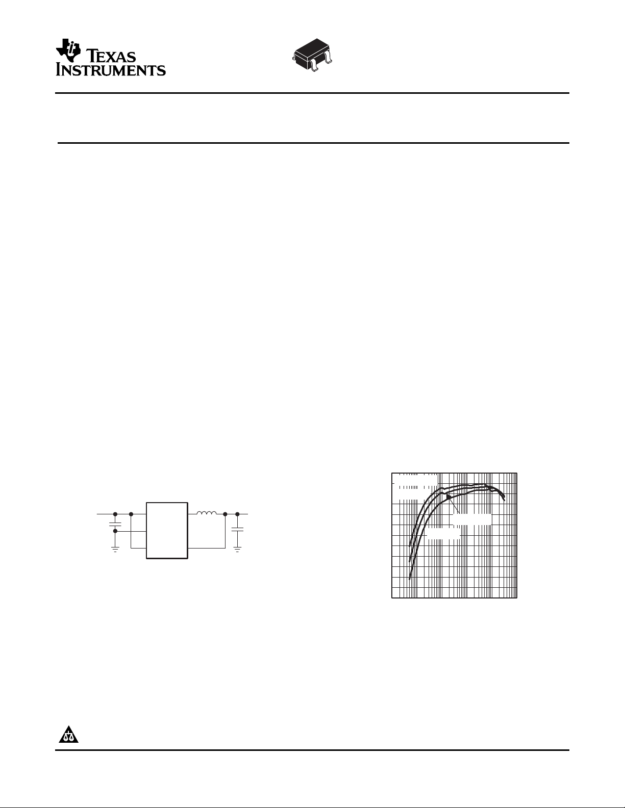
EFFICIENCY
vs
LOAD CURRENT
I
L
−Load Current − mA
V
O
= 1.8 V
V
I
= 2.7 V
V
I
= 3.7 V
V
I
= 5 V
TPS62200 , , TPS62201
TPS62202 , TPS62203 , TPS62207
TPS62204 , TPS62205 , TPS62208
SLVS417E – MARCH 2002 – REVISED MAY 2006
HIGH-EFFICIENCY, SOT23
STEP-DOWN, DC-DC CONVERTER
• High Efficiency Synchronous Step-Down
The TPS6220x devices are a family of high-efficiency
Converter With up to 95% Efficiency
synchronous step-down converters ideally suited for
• 2.5-V to 6-V Input Voltage Range
portable systems powered by 1-cell Li-Ion or 3-cell
• Adjustable Output Voltage Range From 0.7 V
NiMH/NiCd batteries. The devices are also suitable
to V
I
to operate from a standard 3.3-V or 5-V voltage rail.
• Fixed Output Voltage Options Available
With an output voltage range of 6 V down to 0.7 V
• Up to 300 mA Output Current
and up to 300 mA output current, the devices are
ideal to power low voltage DSPs and processors
• 1-MHz Fixed Frequency PWM Operation
used in PDAs, pocket PCs, and smart phones.
• Highest Efficiency Over Wide Load Current
Under nominal load current, the devices operate with
Range Due to Power Save Mode
a fixed switching frequency of typically 1 MHz. At
• 15-µA Typical Quiescent Current
light load currents, the part enters the power save
mode operation; the switching frequency is reduced
• Soft Start
and the quiescent current is typically only 15 µA;
• 100% Duty Cycle Low-Dropout Operation
therefore, it achieves the highest efficiency over the
• Dynamic Output-Voltage Positioning
entire load current range. The TPS6220x needs only
three small external components. Together with the
• Available in a 5-Pin SOT23 Package
SOT23 package, a minimum system solution size is
achieved. An advanced fast response voltage mode
control scheme achieves superior line and load
• PDAs and Pocket PC
regulation with small ceramic input and output
• Cellular Phones, Smart Phones
capacitors.
• Low Power DSP Supply
• Digital Cameras
• Portable Media Players
• Portable Equipment
Figure 1. Typical Application
(Fixed Output Voltage Version)
Please be aware that an important notice concerning availability, standard warranty, and use in critical applications of Texas
Instruments semiconductor products and disclaimers thereto appears at the end of this data sheet.
PRODUCTION DATA information is current as of publication date.
Copyright © 2002–2006, Texas Instruments Incorporated
Products conform to specifications per the terms of the Texas
Instruments standard warranty. Production processing does not
necessarily include testing of all parameters.
www.ti.com
3
2
4
5
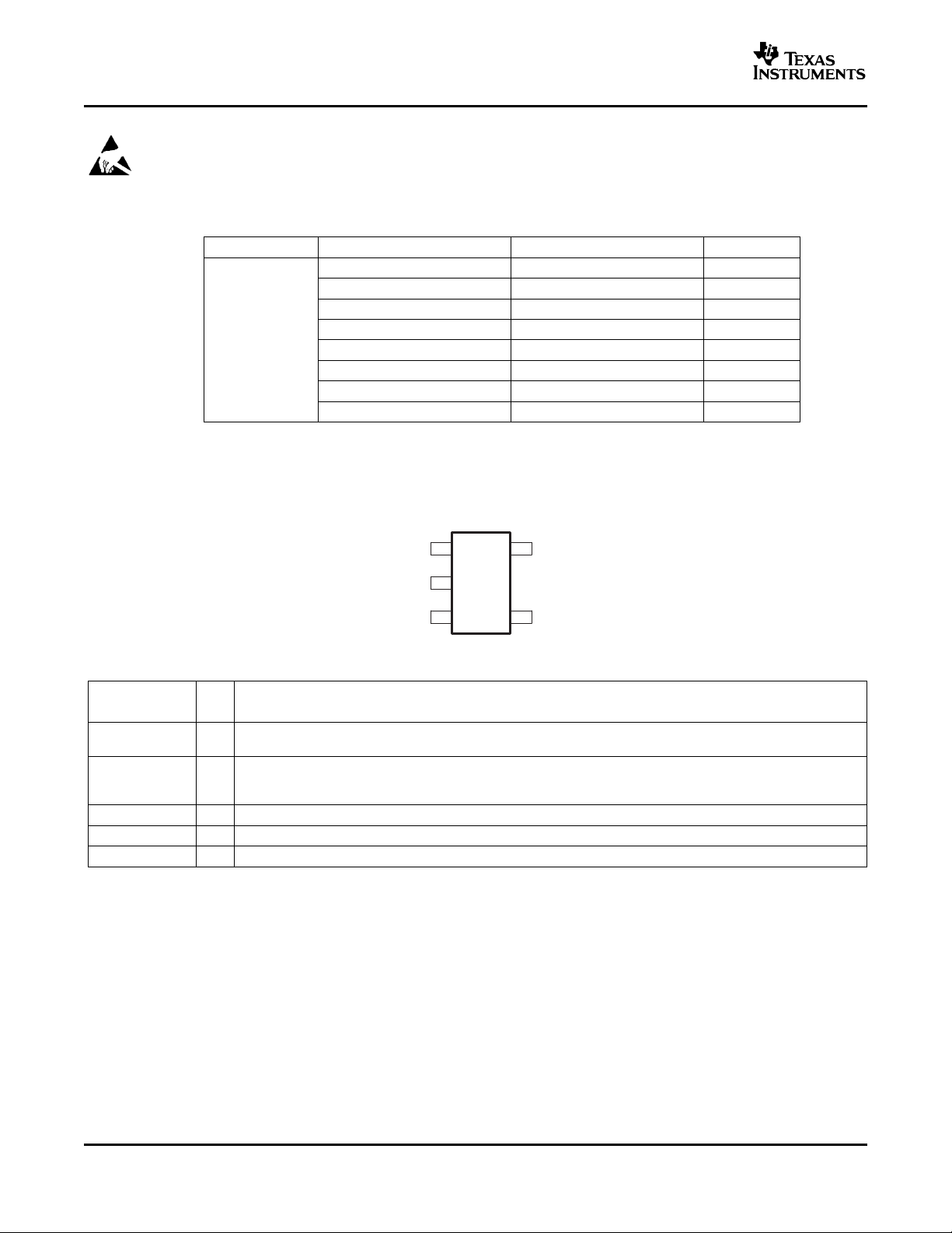
DBV PACKAGE
(TOP VIEW)
1
V
I
GND
EN
SW
FB
TPS62200 , , TPS62201
TPS62202 , TPS62203 , TPS62207
TPS62204 , TPS62205 , TPS62208
SLVS417E – MARCH 2002 – REVISED MAY 2006
This integrated circuit can be damaged by ESD. Texas Instruments recommends that all integrated circuits be handled with
appropriate precautions. Failure to observe proper handling and installation procedures can cause damage.
ESD damage can range from subtle performance degradation to complete device failure. Precision integrated circuits may be
more susceptible to damage because very small parametric changes could cause the device not to meet its published
specifications.
ORDERING INFORMATION
(1)
T
A
OUTPUT VOLTAGE SOT23 PACKAGE SYMBOL
Adjustable TPS62200DBV PHKI
1.2 V TPS62207DBV PJGI
1.5 V TPS62201DBV PHLI
1.6 V TPS62204DBV PHSI
-40°C to 85°C
1.8 V TPS62202DBV PHMI
1.875 V TPS62208DBV ALW
2.5 V TPS62205DBV PHTI
3.3 V TPS62203DBV PHNI
(1) The DBV package is available in tape and reel. Add R suffix (DBVR) to order quantities of 3000 parts.
Add T suffix (DBVT) to order quantities of 250 parts
Terminal Functions
TERMINAL
I/O DESCRIPTION
NAME NO.
This is the enable pin of the device. Pulling this pin to ground forces the device into shutdown mode. Pulling this
EN 3 I
pin to Vin enables the device. This pin must not be left floating and must be terminated.
This is the feedback pin of the device. Connect this pin directly to the output if the fixed output voltage version is
FB 4 I used. For the adjustable version an external resistor divider is connected to this pin. The internal voltage divider
is disabled for the adjustable version.
GND 2 Ground
SW 5 I/O Connect the inductor to this pin. This pin is the switch pin and is connected to the internal MOSFET switches.
V
I
1 I Supply voltage pin
2
Submit Documentation Feedback
www.ti.com
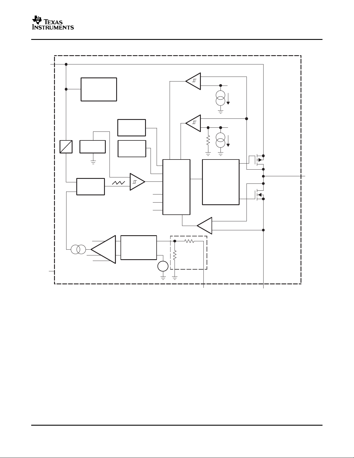
_
+
_
+
_
+
_
+
_
+
REF
REF
Load Comparator
Skip Comparator
Current Limit Comparator
P-Channel
Power MOSFET
Driver
Shoot-Through
Logic
Control
Logic
Soft Start
1 MHz
Oscillator
Comparator
S
R
N-Channel
Power MOSFET
Comparator High
Comparator Low
Comparator Low 2
V
(COMP)
Sawtooth
Generator
V
I
Undervoltage
Lockout
Bias Supply
_
+
Comparator High
Comparator Low
Comparator Low 2
Compensation
V
REF
= 0.5 V
R2
See Note
R1
V
I
EN
SW
FB GND
Gm
DETAILED DESCRIPTION
OPERATION
TPS62200 , , TPS62201
TPS62202 , TPS62203 , TPS62207
TPS62204 , TPS62205 , TPS62208
SLVS417E – MARCH 2002 – REVISED MAY 2006
FUNCTIONAL BLOCK DIAGRAM
For the adjustable version (TPS62200) the internal feedback divider is disabled and the FB pin is directly connected
to the internal GM amplifier
The TPS6220x is a synchronous step-down converter operating with typically 1-MHz fixed frequency pulse width
modulation (PWM) at moderate to heavy load currents and in power save mode operating with pulse frequency
modulation (PFM) at light load currents.
During PWM operation the converter uses a unique fast response, voltage mode, controller scheme with input
voltage feed forward. This achieves good line and load regulation and allows the use of small ceramic input and
output capacitors. At the beginning of each clock cycle initiated by the clock signal (S), the P-channel MOSFET
switch is turned on, and the inductor current ramps up until the comparator trips and the control logic turns off
the switch. The current limit comparator also turns off the switch in case the current limit of the P-channel switch
is exceeded. Then the N-channel rectifier switch is turned on and the inductor current ramps down. The next
cycle is initiated by the clock signal again turning off the N-channel rectifier and turning on the P-channel switch.
3
Submit Documentation Feedback
www.ti.com
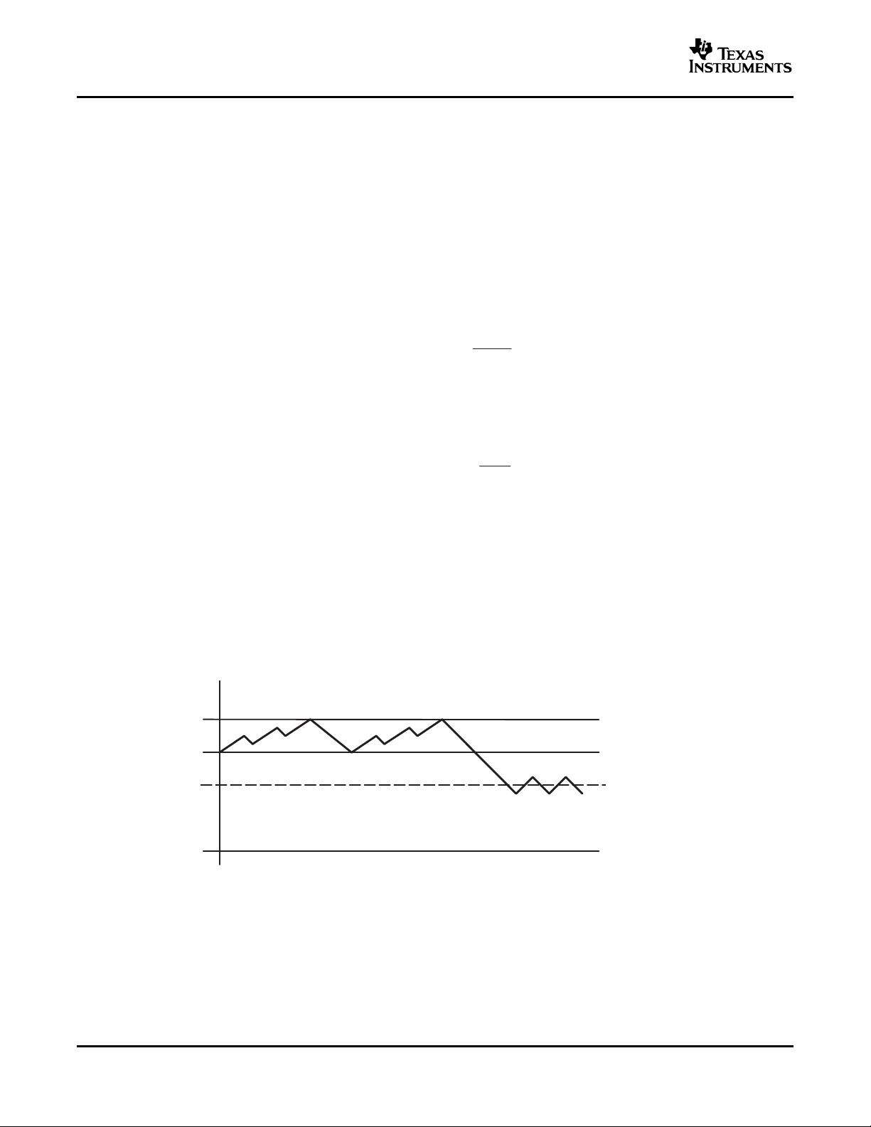
POWER SAVE MODE OPERATION
I
skip
v 66 mA )
Vin
160 W
I
peak
+ 66 mA )
Vin
80 W
PFM Mode at Light Load
Comparator High
Comparator Low
Comparator Low 2
PWM Mode at Medium to Full Load
1.6%
0.8%
V
O
TPS62200 , , TPS62201
TPS62202 , TPS62203 , TPS62207
TPS62204 , TPS62205 , TPS62208
SLVS417E – MARCH 2002 – REVISED MAY 2006
DETAILED DESCRIPTION (continued)
The GM amplifier and input voltage determines the rise time of the Sawtooth generator; therefore any change in
input voltage or output voltage directly controls the duty cycle of the converter. This gives a very good line and
load transient regulation.
As the load current decreases, the converter enters the power save mode operation. During power save mode,
the converter operates with reduced switching frequency in PFM mode and with a minimum quiescent current to
maintain high efficiency.
Two conditions allow the converter to enter the power save mode operation. One is when the converter detects
the discontinuous conduction mode. The other is when the peak switch current in the P-channel switch goes
below the skip current limit. The typical skip current limit can be calculated as
During the power save mode the output voltage is monitored with the comparator by the thresholds comp low
and comp high. As the output voltage falls below the comp low threshold set to typically 0.8% above Vout
nominal, the P-channel switch turns on. The P-channel switch is turned off as the peak switch current is
reached. The typical peak switch current can be calculated:
The N-channel rectifier is turned on and the inductor current ramps down. As the inductor current approaches
zero the N-channel rectifier is turned off and the P-channel switch is turned on again, starting the next pulse.
The converter continues these pulses until the comp high threshold (set to typically 1.6% above Vout nominal) is
reached. The converter enters a sleep mode, reducing the quiescent current to a minimum. The converter
wakes up again as the output voltage falls below the comp low threshold again. This control method reduces the
quiescent current typically to 15 µA and reduces the switching frequency to a minimum, thereby achieving the
high converter efficiency. Setting the skip current thresholds to typically 0.8% and 1.6% above the nominal
output voltage at light load current results in a dynamic output voltage achieving lower absolute voltage drops
during heavy load transient changes. This allows the converter to operate with a small output capacitor of just 10
µF and still have a low absolute voltage drop during heavy load transient changes. Refer to Figure 2 for detailed
operation of the power save mode.
Figure 2. Power Save Mode Thresholds and Dynamic Voltage Positioning
The converter enters the fixed frequency PWM mode again as soon as the output voltage falls below the comp
low 2 threshold.
4
Submit Documentation Feedback

www.ti.com
DYNAMIC VOLTAGE POSITIONING
SOFT START
LOW DROPOUT OPERATION 100% DUTY CYCLE
Vin
min
+ Vout
max
) Iout
max
ǒ
r
ds
(ON)
max
) R
L
Ǔ
Iout
max
= maximum output current plus inductor ripple current
r
ds
(ON)
max
= maximum P-channel switch r
ds
(ON)
R
L
= DC resistance of the inductor
Vout
max
= nominal output voltage plus maximum output voltage tolerance
ENABLE
UNDERVOLTAGE LOCKOUT
TPS62200 , , TPS62201
TPS62202 , TPS62203 , TPS62207
TPS62204 , TPS62205 , TPS62208
SLVS417E – MARCH 2002 – REVISED MAY 2006
DETAILED DESCRIPTION (continued)
As described in the power save mode operation sections and as detailed in Figure 2 , the output voltage is
typically 0.8% above the nominal output voltage at light load currents, as the device is in power save mode. This
gives additional headroom for the voltage drop during a load transient from light load to full load. During a load
transient from full load to light load, the voltage overshoot is also minimized due to active regulation turning on
the N-channel rectifier switch.
The TPS6220x has an internal soft start circuit that limits the inrush current during start-up. This prevents
possible voltage drops of the input voltage in case a battery or a high impedance power source is connected to
the input of the TPS6220x.
The soft start is implemented as a digital circuit increasing the switch current in steps of typically 60 mA,120 mA,
240 mA and then the typical switch current limit of 480 mA. Therefore the start-up time mainly depends on the
output capacitor and load current. Typical start-up time with 10 µF output capacitor and 200 mA load current is
800 µs.
The TPS6220x offers a low input to output voltage difference, while still maintaining operation with the 100%
duty cycle mode. In this mode, the P-channel switch is constantly turned on. This is particularly useful in battery
powered applications to achieve longest operation time by taking full advantage of the whole battery voltage
range. The minimum input voltage to maintain regulation, depending on the load current and output voltage, can
be calculated as
Pulling the enable low forces the part into shutdown, with a shutdown quiescent current of typically 0.1 µA. In
this mode, the P-channel switch and N-channel rectifier are turned off, the internal resistor feedback divider is
disconnected, and the whole device is in shutdown mode. If an output voltage, which could be an external
voltage source or super cap, is present during shutdown, the reverse leakage current is specified under
electrical characteristics. For proper operation the enable pin must be terminated and must not be left floating.
Pulling the enable high starts up the TPS6220x with the soft start as previously described.
The undervoltage lockout circuit prevents the device from misoperation at low input voltages. It prevents the
converter from turning on the switch or rectifier MOSFET under undefined conditions.
5
Submit Documentation Feedback

www.ti.com
ABSOLUTE MAXIMUM RATINGS
DISSIPATION RATING TABLE
RECOMMENDED OPERATING CONDITIONS
ELECTRICAL CHARACTERISTICS
TPS62200 , , TPS62201
TPS62202 , TPS62203 , TPS62207
TPS62204 , TPS62205 , TPS62208
SLVS417E – MARCH 2002 – REVISED MAY 2006
over operating free-air temperature (unless otherwise noted)
(1)
UNIT
Supply voltages, V
I
(2)
-0.3 V to 7.0 V
Voltages on pins SW, EN, FB
(2)
-0.3 V to V
CC
+0.3 V
Continuous power dissipation, P
D
See Dissipation Rating Table
Operating junction temperature range, T
J
-40°C to 150°C
Storage temperature, T
stg
-65°C to 150°C
Lead temperature (soldering, 10 sec) 260°C
(1) Stresses beyond those listed under "absolute maximum ratings" may cause permanent damage to the device. These are stress ratings
only, and functional operation of the device at these or any other conditions beyond those indicated under "recommended operating
conditions" is not implied. Exposure to absolute-maximum-rated conditions for extended periods may affect device reliability.
(2) All voltage values are with respect to network ground terminal.
T
A
≤ 25°C T
A
= 70°C T
A
= 85°C
PACKAGE R
θ JA
POWER RATING POWER RATING POWER RATING
DBV 250°/W 400 mW 220 mW 160 mW
MIN NOM MAX UNIT
Supply voltage, V
I
2.5 6.0 V
Output voltage range for adjustable output voltage version, V
O
0.7 V
I
V
Output current, I
O
300 mA
Inductor, L
(1)
4.7 10 µH
Input capacitor, C
I
(1)
4.7 µF
Output capacitor, C
O
(1)
10 µF
Operating ambient temperature, T
A
40 85 °C
Operating junction temperature, T
J
40 125 °C
(1) See the application section for further information.
V
I
= 3.6 V, V
O
= 1.8 V, I
O
= 200 mA, EN = VIN, T
A
= -40 °C to 85 °C, typical values are at T
A
= 25 °C (unless otherwise noted)
PARAMETER TEST CONDITIONS MIN TYP MAX UNIT
SUPPLY CURRENT
V
I
Input voltage range 2.5 6.0 V
I
Q
Operating quiescent current I
O
= 0 mA, Device is not switching 15 30 µA
Shutdown supply current EN = GND 0.1 1 µA
Undervoltage lockout threshold 1.5 2.0 V
ENABLE
V
(EN)
EN high level input voltage 1.3 V
EN low level input voltage 0.4 V
I
(EN)
EN input bias current EN = GND or VIN 0.01 0.1 µA
POWER SWITCH
V
IN
= V
GS
= 3.6 V 530 690
P-channel MOSFET on-resistance m Ω
V
IN
= V
GS
= 2.5 V 670 850
r
ds
(ON)
V
IN
= V
GS
= 3.6 V 430 540
N-channel MOSFET on-resistance m Ω
V
IN
= V
GS
= 2.5 V 530 660
I
lkg_(P)
P-channel leakage current V
DS
= 6.0 V 0.1 1 µA
6
Submit Documentation Feedback
www.ti.com
TPS62200 , , TPS62201
TPS62202 , TPS62203 , TPS62207
TPS62204 , TPS62205 , TPS62208
SLVS417E – MARCH 2002 – REVISED MAY 2006
ELECTRICAL CHARACTERISTICS (continued)
V
I
= 3.6 V, V
O
= 1.8 V, I
O
= 200 mA, EN = VIN, T
A
= -40 °C to 85 °C, typical values are at T
A
= 25 °C (unless otherwise noted)
PARAMETER TEST CONDITIONS MIN TYP MAX UNIT
I
lkg_(N)
N-channel leakage current V
DS
= 6.0 V 0.1 1 µA
I
(LIM)
P-channel current limit 2.5 V < Vin < 6.0 V 380 480 670 mA
OSCILLATOR
f
S
Switching frequency 650 1000 1500 kHz
OUTPUT
Adjustable output voltage
V
O
TPS62200 0.7 V
IN
V
range
V
ref
Reference voltage 0.5 V
TPS62200 V
I
= 3.6 V to 6.0 V, I
O
= 0 mA 0% 3%
Feedback voltage
(1)
Adjustable V
I
= 3.6 V to 6.0 V, 0 mA ≤ I
O
≤ 300 mA -3% 3%
TPS62207 V
I
= 2.5 V to 6.0 V, I
O
= 0 mA 0% 3%
1.2 V V
I
= 2.5 V to 6.0 V, 0 mA ≤ I
O
≤ 300 mA -3% 3%
TPS62201 V
I
= 2.5 V to 6.0 V, I
O
= 0 mA 0% 3%
1.5 V V
I
= 2.5 V to 6.0 V, 0 mA ≤ I
O
≤ 300 mA -3% 3%
TPS62204 V
I
= 2.5 V to 6.0 V, I
O
= 0 mA 0% 3%
1.6 V V
I
= 2.5 V to 6.0 V, 0 mA ≤ I
O
≤ 300 mA -3% 3%
TPS62202 V
I
= 2.5 V to 6.0 V, I
O
= 0 mA 0% 3%
V
O
Fixed output voltage
(1)
1.8 V V
I
= 2.5 V to 6.0 V, 0 mA ≤ I
O
≤ 300 mA -3% 3%
TPS62208 V
I
= 2.5 V to 6.0 V, I
O
= 0 mA 0% 3%
1.875 V V
I
= 2.5 V to 6.0 V, 0 mA ≤ I
O
≤ 300 mA -3% 3%
TPS62205 V
I
= 2.7 V to 6.0 V, I
O
= 0 mA 0% 3%
2.5 V V
I
= 2.7 V to 6.0 V, 0 mA ≤ I
O
≤ 300 mA -3% 3%
TPS62203 V
I
= 3.6 V to 6.0 V, I
O
= 0 mA 0% 3%
3.3 V V
I
= 3.6 V to 6.0 V, 0 mA ≤ I
O
≤ 300 mA -3% 3%
Line regulation V
I
= 2.5 V to 6.0 V, I
O
= 10 mA 0.26 %/V
Load regulation I
O
= 100 mA to 300 mA 0.0014 %/mA
I
lkg
Leakage current into SW pin Vin > Vout, 0 V ≤ Vsw ≤ Vin 0.1 1 µA
I
lkg
(Rev) Reverse leakage current into pin SW Vin = open, EN = GND, V
SW
= 6.0 V 0.1 1 µA
(1) For output voltages ≤ 1.2 V a 22 µF output capacitor value is required to achieve a maximum output voltage accuracy of 3% while
operating in power save mode (PFM mode)
7
Submit Documentation Feedback
Loading...