


Texas Instruments TPS2206IDFR, TPS2206IDFLE, TPS2206IDBR, TPS2206IDBLE, TPS2206IDB Datasheet
...TPS2206 DUAL-SLOT PC CARD POWER-INTERFACE SWITCH WITH RESET FOR SERIAL PCMCIA CONTROLLER
SLVS138B ± MAY 1996 ± REVISED JUNE 1998
DFully Integrated VCC and Vpp Switching for Dual-Slot PC Card Interface
DP2C 3-Lead Serial Interface Compatible With CardBus Controllers
D3.3 V Low-Voltage Mode
DMeets PC Card Standards
DRESET for System Initialization of PC Cards
D12-V Supply Can Be Disabled Except During
12-V Flash Programming
DShort Circuit and Thermal Protection
D30-Pin SSOP (DB) and 32-Pin TSSOP (DAP)
DCompatible With 3.3-V, 5-V and 12-V PC Cards
DLow rDS(on) (140-mΩ 5-V VCC Switch; 110-mΩ
3.3-V VCC Switch)
DBreak-Before-Make Switching
description
DB OR DF PACKAGE
(TOP VIEW)
|
5V |
|
|
1 |
30 |
|
|
5V |
|
|
|
|
|
|
|||||
|
5V |
|
2 |
29 |
|
|
NC |
||
|
|
|
|
|
|||||
|
DATA |
|
3 |
28 |
|
|
NC |
||
|
|
|
|
|
|||||
CLOCK |
|
4 |
27 |
|
|
NC |
|||
|
|
|
|
||||||
|
LATCH |
|
5 |
26 |
|
|
NC |
||
|
|
|
|
|
|||||
|
|
|
|
|
|||||
|
RESET |
|
6 |
25 |
|
|
NC |
||
|
|
|
|
|
|||||
|
|
|
|
|
|||||
|
12V |
|
7 |
24 |
|
|
12V |
||
|
|
|
|
|
|||||
|
AVPP |
|
8 |
23 |
|
|
BVPP |
||
|
|
|
|
|
|||||
|
|
|
|
|
|||||
|
AVCC |
|
9 |
22 |
|
|
BVCC |
||
|
|
|
|
|
|||||
|
AVCC |
|
10 |
21 |
|
|
BVCC |
||
|
|
|
|
|
|||||
|
|
|
|
|
|||||
|
AVCC |
|
11 |
20 |
|
|
BVCC |
||
|
|
|
|
|
|||||
|
GND |
|
12 |
19 |
|
|
NC |
||
|
|
|
|
|
|||||
|
NC |
|
13 |
18 |
|
|
OC |
||
|
|
|
|
|
|||||
|
|
|
|
|
|||||
|
RESET |
|
|
|
14 |
17 |
|
|
3.3V |
|
|
|
|
|
|
||||
|
|
|
|
|
|
||||
|
3.3V |
|
15 |
16 |
|
|
3.3V |
||
|
|
|
|
|
|||||
|
|
|
|
|
|||||
|
|
|
|
|
|
|
|
|
|
DAP PACKAGE (TOP VIEW)
The TPS2206 PC Card power-interface switch provides an integrated power-management solution for two PC Cards. All of the discrete power MOSFETs, a logic section, current limiting, and thermal protection for PC Card control are combined on a single integrated circuit (IC), using the Texas Instruments LinBiCMOS process. The circuit allows the distribution of 3.3-V, 5-V, and/or 12-V card power by means of the P2C (PCMCIA Peripheral-Control) Texas Instruments nonproprietary serial interface. The current-limiting feature eliminates the need for fuses, which reduces component count and improves reliability.
The TPS2206 is backward compatible with the TPS2202 and TPS2202A, except that there is no VDD connection. Bias current is derived from either the 3.3-V input pin or the 5-V input pin. The TPS2206 also eliminates the APWR_GOOD and BPWR_GOOD pins of the TPS2202 and TPS2202A.
|
5V |
|
|
1 |
32 |
|
|
5V |
|
|
|
|
|
|
|||||
|
5V |
|
2 |
31 |
|
|
NC |
||
|
|
|
|
|
|||||
|
NC |
|
3 |
30 |
|
|
NC |
||
|
|
|
|
|
|||||
|
DATA |
|
4 |
29 |
|
|
NC |
||
|
|
|
|
|
|||||
CLOCK |
|
5 |
28 |
|
|
NC |
|||
|
|
|
|
||||||
|
|
|
|
||||||
|
LATCH |
|
6 |
27 |
|
|
NC |
||
|
|
|
|
|
|||||
|
|
|
|
|
|||||
|
RESET |
|
7 |
26 |
|
|
NC |
||
|
|
|
|
|
|||||
|
12V |
|
8 |
25 |
|
|
12V |
||
|
|
|
|
|
|||||
|
|
|
|
|
|||||
|
AVPP |
|
9 |
24 |
|
|
BVPP |
||
|
|
|
|
|
|||||
|
AVCC |
|
10 |
23 |
|
|
BVCC |
||
|
|
|
|
|
|||||
|
|
|
|
|
|||||
|
AVCC |
|
11 |
22 |
|
|
BVCC |
||
|
|
|
|
|
|||||
|
AVCC |
|
12 |
21 |
|
|
BVCC |
||
|
|
|
|
|
|||||
|
GND |
|
13 |
20 |
|
|
OC |
||
|
|
|
|
|
|||||
|
|
|
|
|
|||||
|
RESET |
|
|
|
14 |
19 |
|
|
NC |
|
|
|
|
|
|
||||
|
|
|
|
|
|
||||
|
NC |
|
15 |
18 |
|
|
3.3V |
||
|
|
|
|
|
|||||
|
|
|
|
|
|||||
|
3.3V |
|
16 |
17 |
|
|
3.3V |
||
|
|
|
|
|
|||||
|
|
|
|
|
|
|
|
|
|
NC ± No internal connection
The TPS2206 features a 3.3-V low-voltage mode that allows for 3.3-V switching without the need for 5 V. This facilitates low-power system designs such as sleep mode and pager mode where only 3.3 V is available.
Please be aware that an important notice concerning availability, standard warranty, and use in critical applications of Texas Instruments semiconductor products and disclaimers thereto appears at the end of this data sheet.
LinBiCMOS and P2C are trademarks of Texas Instruments Incorporated.
PC Card and CardBus are trademarks of PCMCIA (Personal Computer Memory Card International Association).
PRODUCTION DATA information is current as of publication date. Products conform to specifications per the terms of Texas Instruments standard warranty. Production processing does not necessarily include testing of all parameters.
Copyright 1998, Texas Instruments Incorporated
POST OFFICE BOX 655303 •DALLAS, TEXAS 75265 |
1 |
TPS2206
DUAL-SLOT PC CARD POWER-INTERFACE SWITCH
WITH RESET FOR SERIAL PCMCIA CONTROLLER
SLVS138B ± MAY 1996 ± REVISED JUNE 1998
description (continued)
The TPS2206 incorporates a reset function, selectable by one of two inputs, to help alleviate system errors. The reset function enables PC Card initialization concurrent with host platform initialization, allowing a system reset. Reset is accomplished by grounding the VCC and Vpp (flash-memory programming voltage) outputs, which discharges residual card voltage.
End equipment for the TPS2206 includes notebook computers, desktop computers, personal digital assistants (PDAs), digital cameras and bar-code scanners.
AVAILABLE OPTIONS
TA |
|
PACKAGED DEVICES |
|
CHIP FORM (Y) |
|
|
|
|
|
||
PLASTIC SMALL OUTLINE (DB) |
|
PLASTIC SMALL OUTLINE (DF) |
TSSOP (DAP) |
||
|
|
|
|||
|
|
|
|
|
|
± 40°C to 85°C |
TPS2206IDBLE |
|
TPS2206IDFLE |
TPS2206IDAPR |
TPS2206Y |
|
|
|
|
|
|
The DB package and the DF package are only available left-end taped and reeled (indicated by the LE suffix on the device type; e.g., TPS2206IDBLE). The DAP package is only available taped and reeled (indicated by the R suffix on the device type; e.g., TPS2206IDAPR).
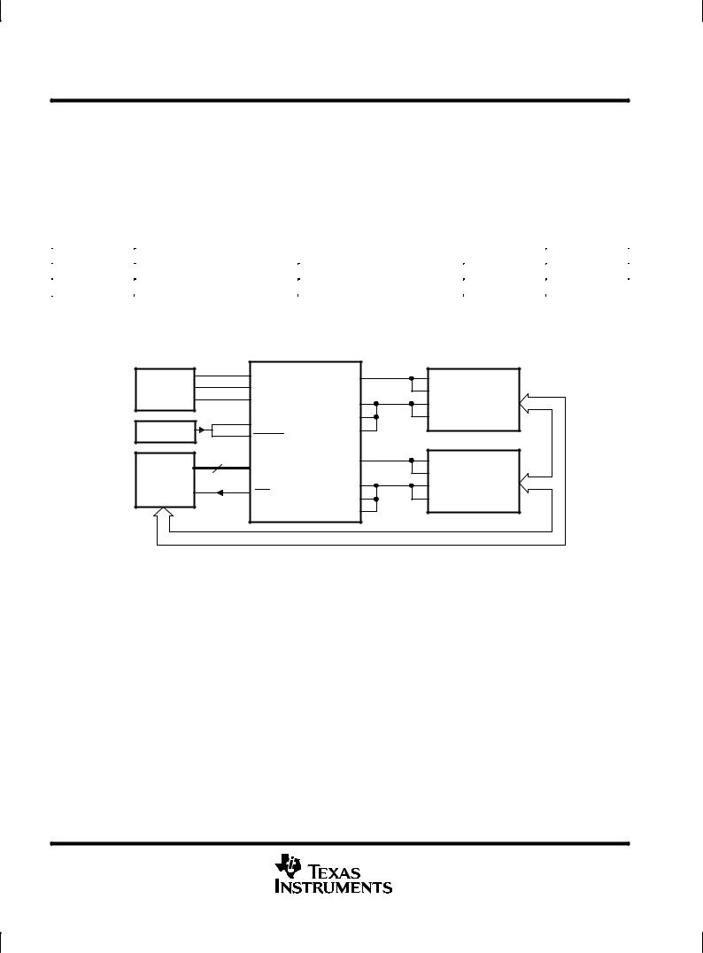
typical PC card power-distribution application
Power Supply |
TPS2206 |
|
|
|
|
||
12 V |
12V |
AVPP |
|
5 V |
5V |
|
|
3.3 V |
3.3V |
AVCC |
|
|
RESET |
AVCC |
|
Supervisor |
AVCC |
||
RESET |
|||
|
|
||
3 |
Serial Interface |
BVPP |
|
PCMCIA |
|
||
|
|
||
Controller |
OC |
BVCC |
|
|
BVCC |
||
|
|
||
|
|
BVCC |
Vpp1 |
|
Vpp2 |
PC |
VCC |
Card A |
VCC |
|
Vpp1 |
|
Vpp2 |
PC |
VCC |
Card B |
VCC |
|
2 |
POST OFFICE BOX 655303 •DALLAS, TEXAS 75265 |
TPS2206
DUAL-SLOT PC CARD POWER-INTERFACE SWITCH
WITH RESET FOR SERIAL PCMCIA CONTROLLER
SLVS138B ± MAY 1996 ± REVISED JUNE 1998
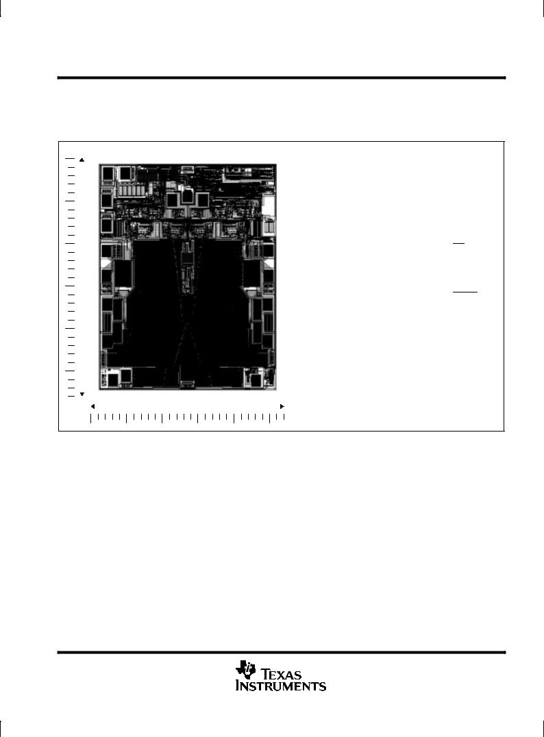
TPS2206Y chip information
This chip, when properly assembled, displays characteristics similar to those of the TPS2206. Thermal compression or ultrasonic bonding may be used on the doped-aluminum bonding pads. The chips may be mounted with conductive epoxy or a gold-silicon preform.
BONDING PAD ASSIGNMENTS
|
|
|
|
|
4 |
3 |
|
|
|
|
|
|
|
|
|
|
|
5 |
|
2 |
1 |
23 |
|
|
|
|
|
|
|
|
|
|
|
|||||
|
|
|
6 |
|
|
|
|
|
|
|
||
|
|
|
7 |
|
|
|
|
|
22 |
|
||
|
|
|
8 |
|
|
|
|
|
21 |
|
||
|
|
|
|
|
|
|
||||||
144 |
|
|
|
|
|
|
|
|
||||
|
9 |
|
|
|
|
|
20 |
|
||||
|
|
|
|
|
|
|
|
|
||||
|
|
|
10 |
|
|
|
|
|
19 |
|
||
|
|
|
11 |
|
|
|
|
|
18 |
|
||
|
|
|
|
|
12 |
13 |
14 |
15 |
16 |
17 |
|
|
|
|
|
|
|
|
|||||||
|
|
|
|
|
|
|
|
|
|
|
|
|
|
|
|
|
|
|
|
142 |
|
|
|
|
|
|
|
|
|
|
|
|
|
|
|
|
|
|
|
|
|
|
|
|
|
|
|
|
|
|
|
5V |
|
1 |
TPS2206Y |
|
|
|
|||
5V |
|
2 |
23 |
|
|
|
|||
DATA |
|
3 |
22 |
|
|
|
|||
CLOCK |
|
4 |
21 |
|
|
|
|||
LATCH |
|
5 |
20 |
|
|
|
|||
RESET |
|
6 |
19 |
|
|
|
|||
12V |
|
7 |
18 |
|
|
|
|||
AVPP |
|
8 |
17 |
|
|
|
|||
AVCC |
|
9 |
16 |
|
|
|
|||
AVCC |
|
10 |
15 |
|
|
|
|||
AVCC |
|
11 |
14 |
|
|
|
|||
GND |
|
12 |
13 |
|
|
|
|||
|
|
|
|
|
CHIP THICKNESS: 15 TYPICAL BONDING PADS: 4 × 4 MINIMUM TJ max = 150°C
TOLERANCES ARE ± 10%.
ALL DIMENSIONS ARE IN MILS.
5V
12V
BVPP
BVCC
BVCC
BVCC
OC
3.3V
3.3V
3.3V
RESET
POST OFFICE BOX 655303 •DALLAS, TEXAS 75265 |
3 |

TPS2206
DUAL-SLOT PC CARD POWER-INTERFACE SWITCH
WITH RESET FOR SERIAL PCMCIA CONTROLLER
SLVS138B ± MAY 1996 ± REVISED JUNE 1998
|
|
|
|
|
|
|
|
Terminal Functions |
||||
|
|
|
|
|
|
|
|
|
|
|
|
|
|
|
|
|
TERMINAL |
|
|
|
|
|
|
|
|
|
|
|
|
|
|
|
|
|
|
|
|
|
|
NAME |
NO. |
|
I/O |
|
|
|
|
DESCRIPTION |
|||
|
|
|
|
DB, DF |
|
DAP |
|
|
|
|
|
|
|
|
|
|
|
|
|
|
|
|
|
|
|
|
3.3V |
15, 16, 17 |
|
16, 17, 18 |
I |
3.3-V VCC input for card power |
||||||
|
5V |
1, 2, 30 |
|
1, 2, 32 |
I |
5-V VCC input for card power and/or chip power |
||||||
|
12V |
7, 24 |
|
8, 25 |
I |
12-V Vpp input for card power |
||||||
|
AVCC |
9, 10, 11 |
|
10, 11, 12 |
O |
Switched output that delivers 0 V, 3.3 V, 5 V, or high impedance to card |
||||||
|
|
|
|
|
|
|
|
|
|
|
|
|
|
AVPP |
8 |
|
9 |
O |
Switched output that delivers 0 V, 3.3 V, 5 V, 12 V, or high impedance to card |
||||||
|
|
|
|
|
|
|
|
|
|
|
|
|
|
BVCC |
20, 21, 22 |
|
21, 22, 23 |
O |
Switched output that delivers 0 V, 3.3 V, 5 V, or high impedance |
||||||
|
|
|
|
|
|
|
|
|
|
|
|
|
|
BVPP |
23 |
|
24 |
O |
Switched output that delivers 0 V, 3.3 V, 5 V, 12 V, or high impedance |
||||||
|
|
|
|
|
|
|
|
|
|
|
|
|
|
CLOCK |
4 |
|
5 |
I |
Logic-level clock for serial data word |
||||||
|
|
|
|
|
|
|
|
|
|
|
|
|
|
DATA |
3 |
|
4 |
I |
Logic-level serial data word |
||||||
|
|
|
|
|
|
|
|
|
|
|
|
|
|
GND |
12 |
|
13 |
|
Ground |
||||||
|
|
|
|
|
|
|
|
|
|
|
|
|
|
LATCH |
5 |
|
6 |
I |
Logic-level latch for serial data word |
||||||
|
|
|
|
|
|
|
|
|
|
|
|
|
|
NC |
13, 19, 25, |
|
3, 19, 26, |
|
No internal connection |
||||||
|
|
|
|
26, 27, |
|
27, 28, 29, |
|
|
|
|
|
|
|
|
|
|
28, 29 |
|
30, 31 |
|
|
|
|
|
|
|
|
|
|
|
|
|
|
|
|
|
|
|
|
|
|
|
18 |
|
20 |
O |
Logic-level overcurrent. |
|
reports output that goes low when an overcurrent condition exists |
||
|
OC |
|
|
|
OC |
|||||||
|
|
|
|
|
|
|
|
|
|
|||
|
RESET |
6 |
|
7 |
I |
Logic-level RESET input active high. Do not connect if terminal 14 is used. |
||||||
|
|
|
|
|
|
|
|
|
||||
|
|
|
|
14 |
|
14 |
I |
Logic-level |
|
input active low. Do not connect if terminal 6 is used. |
||
|
RESET |
|
|
RESET |
||||||||
|
|
|
|
|
|
|
|
|
|
|
|
|
absolute maximum ratings over operating free-air temperature (unless otherwise noted)²
Input voltage range for card power: VI(5V) . . . . . . . . . . . . . . . . . . . . . . . . . . . . . . . |
. . . . . . . . . . . . . ±0.3 V to 7 |
V |
VI(3.3V) . . . . . . . . . . . . . . . . . . . . . . . . . . . . . . |
. . . . . . . . . . . . . ±0.3 V to 7 |
V |
VI(12V) . . . . . . . . . . . . . . . . . . . . . . . . . . . . . . |
. . . . . . . . . . . . ±0.3 V to 14 |
V |
Logic input voltage . . . . . . . . . . . . . . . . . . . . . . . . . . . . . . . . . . . . . . . . . . . . . . . . . . . . |
. . . . . . . . . . . . . ±0.3 V to 7 |
V |
Continuous total power dissipation . . . . . . . . . . . . . . . . . . . . . . . . . . . . . . . . . . . . . |
See Dissipation Rating Table |
|
Output current (each card): IO(xVCC) . . . . . . . . . . . . . . . . . . . . . . . . . . . . . . . . . . . . |
. . . . . . . . . . . internally limited |
|
IO(xVPP) . . . . . . . . . . . . . . . . . . . . . . . . . . . . . . . . . . . . |
. . . . . . . . . . . internally limited |
|
Operating virtual junction temperature range, TJ . . . . . . . . . . . . . . . . . . . . . . . . . . |
. . . . . . . . . . . ±40°C to 150°C |
|
Operating free-air temperature range, TA . . . . . . . . . . . . . . . . . . . . . . . . . . . . . . . . |
. . . . . . . . . . . . ±40°C to 85°C |
|
Storage temperature range, Tstg . . . . . . . . . . . . . . . . . . . . . . . . . . . . . . . . . . . . . . . . |
. . . . . . . . . . . ±55°C to 150°C |
|
Lead temperature 1,6 mm (1/16 inch) from case for 10 seconds . . . . . . . . . . . . |
. . . . . . . . . . . . . . . . . . . 260°C |
|
²Stresses beyond those listed under ªabsolute maximum ratingsº may cause permanent damage to the device. These are stress ratings only, and functional operation of the device at these or any other conditions beyond those indicated under ªrecommended operating conditionsº is not implied. Exposure to absolute-maximum-rated conditions for extended periods may affect device reliability.
DISSIPATION RATING TABLE
|
|
T ≤ 25°C |
DERATING FACTOR³ |
T = 70°C |
T = 85°C |
|
PACKAGE |
A |
ABOVE TA = 25°C |
A |
A |
||
POWER RATING |
POWER RATING |
POWER RATING |
||||
|
|
|||||
DB |
1024 mW |
8.2 mW/°C |
655 mW |
532 mW |
||
DF |
1158 mW |
9.26 mW/°C |
741 mW |
602 mW |
||
|
|
|
|
|
|
|
DAP |
No backplane |
1625 mW |
13 mW/°C |
1040 mW |
845 mW |
|
|
|
|
|
|
||
Backplane§ |
6044 mW |
48.36 mW/°C |
3869 mW |
3143 mW |
||
|
||||||
³ These devices are mounted on an FR4 board with no special thermal considerations.
§ 2-oz backplane with 2-oz traces; 5.2-mm × 11-mm thermal pad with 6-mil solder; 0.18-mm diameter vias in a 3×6 array.
4 |
POST OFFICE BOX 655303 •DALLAS, TEXAS 75265 |

TPS2206
DUAL-SLOT PC CARD POWER-INTERFACE SWITCH
WITH RESET FOR SERIAL PCMCIA CONTROLLER
SLVS138B ± MAY 1996 ± REVISED JUNE 1998
recommended operating conditions
|
|
MIN |
MAX |
UNIT |
|
|
|
|
|
|
VI(5V) |
0 |
5.25 |
V |
Input voltage range, VI |
VI(3.3V) |
0 |
5.25 |
V |
|
VI(12V) |
0 |
13.5 |
V |
Output current |
IO(xVCC) at 25°C |
|
1 |
A |
IO(xVPP) at 25°C |
|
150 |
mA |
|
|
|
|||
Clock frequency |
|
0 |
2.5 |
MHz |
|
|
|
|
|
Operating virtual junction temperature, TJ |
± 40 |
125 |
°C |
|
electrical characteristics, TA = 25°C, VI(5V) = 5 V (unless otherwise noted) dc characteristics
|
PARAMETER |
TEST CONDITIONS |
|
TPS2206 |
|
UNIT |
|||
|
|
|
|
||||||
|
MIN |
TYP |
MAX |
||||||
|
|
|
|
|
|
|
|||
|
|
|
|
|
|
|
|
|
|
|
|
5 V to xVCC |
|
|
|
|
103 |
140 |
|
|
|
|
|
|
|
|
|
mΩ |
|
|
|
3.3 V to xVCC |
VI(5V) = 5 V, |
VI(3.3 V) = 3.3 V |
|
69 |
110 |
||
|
Switch resistances² |
3.3 V to xVCC |
VI(5V) = 0, |
|
VI(3.3V) = 3.3 V |
|
96 |
180 |
|
|
5 V to xVPP |
|
|
|
|
|
6 |
|
|
|
|
|
|
|
|
|
|
||
|
|
|
|
|
|
|
|
|
Ω |
|
|
3.3 V to xVPP |
|
|
|
|
|
6 |
|
|
|
|
|
|
|
|
|
|
|
|
|
12 V to xVPP |
|
|
|
|
|
1 |
|
|
|
|
|
|
|
|
|
|
|
VO(xVPP) |
Clamp low voltage |
|
Ipp at 10 mA |
|
|
|
0.8 |
V |
|
VO(xVCC) |
Clamp low voltage |
|
ICC at 10 mA |
|
|
|
0.8 |
V |
|
|
|
Ipp high-impedance state |
TA = 25°C |
|
|
|
1 |
10 |
|
Ilkg |
Leakage current |
TA = 85°C |
|
|
|
|
50 |
μA |
|
|
|
|
|
|
|||||
ICC high-impedance state |
TA = 25°C |
|
|
|
1 |
10 |
|||
|
|
|
|
|
|
||||
|
|
TA = 85°C |
|
|
|
|
50 |
|
|
|
|
|
|
|
|
|
|
||
|
|
VI(5V) = 5 V |
VO(AVCC) |
= VO(BVCC) = 5 V, |
|
117 |
150 |
|
|
|
|
VO(AVPP) = VO(BVPP) = 12 V |
|
|
|||||
|
|
|
|
|
|
μA |
|||
II |
Input current |
VI(5V) = 0, |
VO(AVCC) |
= VO(BVCC) = 3.3 V, |
|
131 |
150 |
||
|
|
||||||||
VI(3.3V) = 3.3 V |
VO(AVPP) = VO(BVPP) = 0 |
|
|
||||||
|
|
|
|
||||||
|
|
Shutdown mode |
VO(BVCC) = VO(AVCC) = VO(AVPP) |
|
|
1 |
μA |
||
|
|
= VO(BVPP) = Hi-Z |
|
|
|
||||
|
|
|
|
|
|
|
|
||
IOS |
Short-circuit |
IO(xVCC) |
TJ = 85°C, |
|
|
1 |
|
2.2 |
A |
output-current limit |
IO(xVPP) |
Output powered up into a short to GND |
120 |
|
400 |
mA |
|||
|
|
|
|
|
|
||||
²Pulse-testing techniques are used to maintain junction temperature close to ambient temperature; thermal effects must be taken into account separately.
logic section
PARAMETER |
TEST CONDITIONS |
TPS2206 |
|
UNIT |
|
|
|
|
|
||||
MIN |
MAX |
|
||||
|
|
|
|
|
||
|
|
|
|
|
|
|
Logic input current |
|
|
|
1 |
μA |
|
|
|
|
|
|
|
|
Logic input high level |
|
|
2 |
|
V |
|
|
|
|
|
|
|
|
Logic input low level |
|
|
|
0.8 |
V |
|
|
|
|
|
|
|
|
|
VI(5V)= 5 V, |
IO = 1mA |
VI(5V)±0.4 |
|
|
|
Logic output high level |
VI(5V)= 0, |
IO = 1mA, |
VI(3.3V)±0.4 |
|
V |
|
|
VI(3.3V) = 3.3 V |
|
|
|
|
|
Logic output low level |
IO = 1mA |
|
|
0.4 |
V |
|
|
|
|
|
|
|
|
|
|
|
|
|
|
|
POST OFFICE BOX 655303 •DALLAS, TEXAS 75265 |
5 |
TPS2206
DUAL-SLOT PC CARD POWER-INTERFACE SWITCH
WITH RESET FOR SERIAL PCMCIA CONTROLLER
SLVS138B ± MAY 1996 ± REVISED JUNE 1998
switching characteristics²³
|
PARAMETER |
TEST CONDITIONS |
|
|
|
TPS2206 |
|
UNIT |
|
|
|
|
|
|
|||
|
|
|
MIN |
TYP |
MAX |
|||
|
|
|
|
|
|
|||
|
|
|
|
|
|
|
|
|
tr |
Output rise time |
VO(xVCC) |
|
|
|
1.2 |
|
|
VO(xVPP) |
|
|
|
5 |
|
ms |
||
|
|
|
|
|
|
|||
tf |
Output fall time |
VO(xVCC) |
|
|
|
10 |
|
|
|
|
|
|
|
||||
VO(xVPP) |
|
|
|
14 |
|
|
||
|
|
|
|
|
|
|
||
|
|
LATCH↑ to VO(xVPP) |
|
ton |
|
4.4 |
|
ms |
|
|
|
toff |
|
18 |
|
ms |
|
|
|
|
|
|
|
|||
|
|
LATCH↑ to VO(xVCC) (3.3 V), VI(5V) |
= 5 V |
ton |
|
6.5 |
|
ms |
tpd |
Propagation delay (see Figure 1) |
toff |
|
20 |
|
ms |
||
|
|
|
|
|||||
LATCH↑ to VO(xVCC) (5 V) |
|
ton |
|
5.7 |
|
ms |
||
|
|
|
|
|
||||
|
|
|
toff |
|
25 |
|
ms |
|
|
|
|
|
|
|
|||
|
|
LATCH↑ to VO(xVCC) (3.3 V), VI(5V) |
= 0 |
ton |
|
6.6 |
|
ms |
|
|
toff |
|
21 |
|
ms |
||
|
|
|
|
|
|
² Refer to Parameter Measurement Information
³ Switching Characteristics are with CL = 150 μF.
electrical characteristics, TA = 25°C, VI(5V) = 5 V (unless otherwise noted)
dc characteristics
|
PARAMETER |
TEST CONDITIONS |
TPS2206Y |
|
UNIT |
|||
|
|
|
|
|||||
|
MIN |
TYP |
MAX |
|||||
|
|
|
|
|
|
|||
|
|
|
|
|
|
|
|
|
|
|
5 V to xVCC |
|
|
|
103 |
|
|
|
|
|
|
|
|
|
|
mΩ |
|
|
3.3 V to xVCC |
VI(5V) = 5 V, |
VI(3.3 V) = 3.3 V |
|
69 |
|
|
|
Switch resistances§ |
3.3 V to xVCC |
VI(5V) = 0, |
VI(3.3V) = 3.3 V |
|
96 |
|
|
|
5 V to xVPP |
|
|
|
4.74 |
|
|
|
|
|
|
|
|
|
|
||
|
|
|
|
|
|
|
|
Ω |
|
|
3.3 V to xVPP |
|
|
|
4.74 |
|
|
|
|
|
|
|
|
|
|
|
|
|
12 V to xVPP |
|
|
|
0.724 |
|
|
|
|
|
|
|
|
|
|
|
VO(xVPP) |
Clamp low voltage |
Ipp at 10 mA |
|
|
0.275 |
|
V |
|
VO(xVCC) |
Clamp low voltage |
ICC at 10 mA |
|
|
0.275 |
|
V |
|
Ilkg |
Leakage current |
Ipp High-impedance state |
TA = 25°C |
|
|
1 |
|
μA |
ICC High-impedance state |
TA = 25°C |
|
|
1 |
|
|||
|
|
|
|
|
|
|||
|
|
VI(5V) = 5 V |
VO(AVCC) = VO(BVCC) = 5 V, |
|
117 |
|
|
|
|
|
VO(AVPP) = VO(BVPP) = 12 V |
|
|
|
|||
II |
Input current |
|
|
|
|
μA |
||
VI(5V) = 0, |
VO(AVCC) = VO(BVCC) = 3.3 V, |
|
131 |
|
||||
|
|
VI(3.3V) = 3.3 V |
VO(AVPP) = VO(BVPP) = 0 |
|
|
|
||
|
|
|
|
|
|
|||
§Pulse-testing techniques are used to maintain junction temperature close to ambient temperature; thermal effects must be taken into account separately.
6 |
POST OFFICE BOX 655303 •DALLAS, TEXAS 75265 |
TPS2206
DUAL-SLOT PC CARD POWER-INTERFACE SWITCH
WITH RESET FOR SERIAL PCMCIA CONTROLLER
SLVS138B ± MAY 1996 ± REVISED JUNE 1998
switching characteristics²³
|
PARAMETER |
TEST CONDITIONS |
|
|
TPS2206Y |
|
UNIT |
|
|
|
|
|
|
|
|||
|
|
|
MIN |
TYP |
MAX |
|||
|
|
|
|
|
|
|||
|
|
|
|
|
|
|
|
|
tr |
Output rise time |
VO(xVCC) |
|
|
|
1.2 |
|
|
VO(xVPP) |
|
|
|
5 |
|
ms |
||
|
|
|
|
|
|
|||
tf |
Output fall time |
VO(xVCC) |
|
|
|
10 |
|
|
|
|
|
|
|
||||
VO(xVPP) |
|
|
|
14 |
|
|
||
|
|
|
|
|
|
|
||
|
|
LATCH↑ to VO(xVPP) |
|
ton |
|
4.4 |
|
ms |
|
|
|
toff |
|
18 |
|
ms |
|
|
|
|
|
|
|
|||
|
|
LATCH↑ to VO(xVCC) (3.3 V), VI(5V) |
= 5 V |
ton |
|
6.5 |
|
ms |
tpd |
Propagation delay (see Figure 1) |
toff |
|
20 |
|
ms |
||
|
|
|
|
|||||
LATCH↑ to VO(xVCC) (5 V) |
|
ton |
|
5.7 |
|
ms |
||
|
|
|
|
|
||||
|
|
|
toff |
|
25 |
|
ms |
|
|
|
|
|
|
|
|||
|
|
LATCH↑ to VO(xVCC) (3.3 V), VI(5V) |
= 0 |
ton |
|
6.6 |
|
ms |
|
|
toff |
|
21 |
|
ms |
||
|
|
|
|
|
|
|||
² Refer to Parameter Measurement Information
³ Switching Characteristics are with CL = 150 μF.
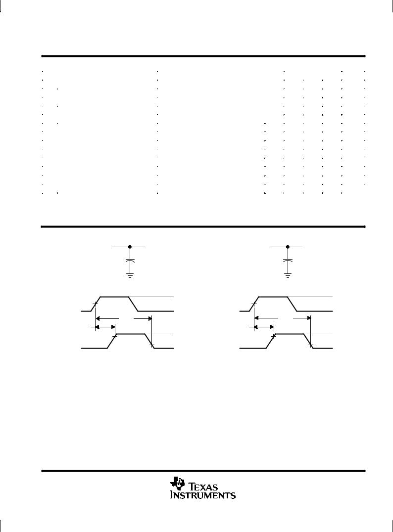
PARAMETER MEASUREMENT INFORMATION
|
Vpp |
|
|
|
VCC |
|
|
|
CL |
|
|
|
CL |
|
|
|
LOAD CIRCUIT |
|
|
|
LOAD CIRCUIT |
|
|
|
50% |
|
VDD |
|
50% |
|
VDD |
LATCH |
|
|
LATCH |
|
|
||
|
|
GND |
|
|
|
GND |
|
|
|
|
|
|
|
||
|
toff |
|
|
|
toff |
|
|
ton |
|
|
|
|
ton |
|
|
|
90% |
|
VI(12V) |
VO(xVCC) |
90% |
|
VI(5V) |
VO(xVPP) |
|
|
|
|
|||
|
10% |
GND |
|
10% |
GND |
||
|
|
|
|
|
|
||
|
VOLTAGE WAVEFORMS |
|
|
|
VOLTAGE WAVEFORMS |
|
|
Figure 1. Test Circuits and Voltage Waveforms
POST OFFICE BOX 655303 •DALLAS, TEXAS 75265 |
7 |
TPS2206
DUAL-SLOT PC CARD POWER-INTERFACE SWITCH
WITH RESET FOR SERIAL PCMCIA CONTROLLER
SLVS138B ± MAY 1996 ± REVISED JUNE 1998
PARAMETER MEASUREMENT INFORMATION
Table of Timing Diagrams
|
|
|
|
|
|
|
|
|
|
FIGURE |
|
|
|
|
|
|
|
|
|
|
|
|
Serial-Interface Timing |
|
|
|
|
|
|
|
2 |
|
|
|
|
|
|||||||
|
xVCC Propagation Delay and Rise Time With 1-μF Load, 3.3-V Switch, VI(5V) = 5 V |
|
3 |
|||||||
|
xVCC Propagation Delay and Fall Time With 1-μF Load, 3.3-V Switch, VI(5V) = 5 V |
|
4 |
|||||||
|
xVCC Propagation Delay and Rise Time With 150-μF Load, 3.3-V Switch, VI(5V) = 5 V |
|
5 |
|||||||
|
xVCC Propagation Delay and Fall Time With 150-μF Load, 3.3-V Switch, VI(5V) = 5 V |
|
6 |
|||||||
|
xVCC Propagation Delay and Rise Time With 1-μF Load, 3.3-V Switch, VI(5V) = 0 |
|
7 |
|||||||
|
xVCC Propagation Delay and Fall Time With 1-μF Load, 3.3-V Switch, VI(5V) = 0 |
|
8 |
|||||||
|
xVCC Propagation Delay and Rise Time With 150-μF Load, 3.3-V Switch, VI(5V) = 0 |
|
9 |
|||||||
|
xVCC Propagation Delay and Fall Time With 150-μF Load, 3.3-V Switch, VI(5V) = 0 |
|
10 |
|||||||
|
xVCC Propagation Delay and Rise Time With 1-μF Load, 5-V Switch |
|
|
|
11 |
|||||
|
|
|
|
|
|
|||||
|
xVCC Propagation Delay and Fall Time With 1-μF Load, 5-V Switch |
|
|
|
12 |
|||||
|
|
|
|
|
||||||
|
xVCC Propagation Delay and Rise Time With 150-μF Load, 5-V Switch |
|
|
13 |
||||||
|
|
|
|
|
||||||
|
xVCC Propagation Delay and Fall Time With 150-μF Load, 5-V Switch |
|
|
14 |
||||||
|
|
|
|
|
||||||
|
xVPP Propagation Delay and Rise Time With 1-μF Load, 12-V Switch |
|
|
15 |
||||||
|
|
|
|
|
|
|||||
|
xVPP Propagation Delay and Fall Time With 1-μF Load, 12-V Switch |
|
|
|
16 |
|||||
|
|
|
|
|
||||||
|
xVPP Propagation Delay and Rise Time With 150-μF Load, 12-V Switch |
|
|
17 |
||||||
|
|
|
|
|
||||||
|
xVPP Propagation Delay and Fall Time With 150-μF Load, 12-V Switch |
|
|
18 |
||||||
|
|
|
|
|
|
|
|
|
|
|
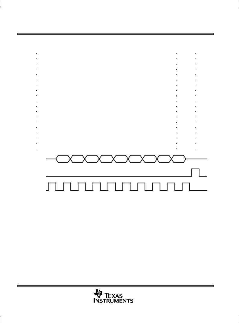
DATA |
D8 |
D7 |
D6 |
D5 |
D4 |
D3 |
D2 |
D1 |
D0 |
|
LATCH
CLOCK
NOTE A: Data is clocked in on the positive leading edge of the clock. The latch should occur before the next positive leading edge of the clock. For definition of D0 to D8, see the control logic table.
Figure 2. Serial-Interface Timing
8 |
POST OFFICE BOX 655303 •DALLAS, TEXAS 75265 |

TPS2206
DUAL-SLOT PC CARD POWER-INTERFACE SWITCH
WITH RESET FOR SERIAL PCMCIA CONTROLLER
SLVS138B ± MAY 1996 ± REVISED JUNE 1998
PARAMETER MEASUREMENT INFORMATION
|
|
|
|
|
|
LATCH (2 V/div) |
|
|
|
|
|
|
|
LATCH (2 V/div) |
|
||||
|
xVCC (2 V/div) |
|
|
|
|
|
|
|
|
|
|
|
|
xVCC (2 V/div) |
|
||||
|
|
|
|
|
|
|
|
|
|
|
|
|
|
|
|
|
|||
0 |
1 |
2 |
3 |
4 |
5 |
6 |
7 |
8 |
9 |
0 |
5 |
10 |
15 |
20 |
25 |
30 |
35 |
40 |
45 |
|
|
|
t ± Time ± ms |
|
|
|
|
|
|
|
t ± Time ± ms |
|
|
|
|
||||
Figure 3. xVCC Propagation Delay and |
Figure 4. xVCC Propagation Delay and |
Rise Time With 1-μF Load, 3.3-V Switch, |
Fall Time With 1-μF Load, 3.3-V Switch, |
(VI(5 V) = 5 V) |
(VI(5 V) = 5 V) |
|
|
|
|
|
|
LATCH (2 V/div) |
|
|
|
|
|
|
|
LATCH (2 V/div) |
|
||||
|
|
|
|
|
|
|
|
|
|
|
|
|
|
|
|
|
|||
|
xVCC (2 V/div) |
|
|
|
|
|
|
|
|
|
|
|
|
xVCC (2 V/div) |
|
||||
|
|
|
|
|
|
|
|
|
|
|
|
|
|
|
|
|
|||
0 |
1 |
2 |
3 |
4 |
5 |
6 |
7 |
8 |
9 |
0 |
5 |
10 |
15 |
20 |
25 |
30 |
35 |
40 |
45 |
|
|
|
t ± Time ± ms |
|
|
|
|
|
|
|
t ± Time ± ms |
|
|
|
|
||||
Figure 5. xVCC Propagation Delay and |
Figure 6. xVCC Propagation Delay and |
Rise Time With 150-μF Load, 3.3-V Switch, |
Fall Time With 150-μF Load, 3.3-V Switch, |
VI(5 V) = 5 V |
VI(5 V) = 5 V |
POST OFFICE BOX 655303 •DALLAS, TEXAS 75265 |
9 |
 Loading...