


Texas Instruments TLC251CD, TLC251CDR, TLC251BCP, TLC251ACP, TLC251ACDR Datasheet
...
|
|
|
TLC251, TLC251A, TLC251B, TLC251Y |
|||||||||||||
|
|
|
LinCMOS |
PROGRAMMABLE |
||||||||||||
|
|
|
LOW-POWER OPERATIONAL AMPLIFIERS |
|||||||||||||
|
|
|
SLOS001E ± JULY 1983 ± REVISED AUGUST 1994 |
|||||||||||||
|
|
|
|
|
|
|
|
|
|
|
|
|
|
|
||
D Wide Range of Supply Voltages |
D OR P PACKAGE |
|||||||||||||||
1.4 V to 16 V |
|
|
|
(TOP VIEW) |
|
|
|
|
|
|||||||
D True Single-Supply Operation |
OFFSET N1 |
|
|
|
|
|
|
|
BIAS SELECT |
|||||||
|
|
1 |
8 |
|||||||||||||
|
|
|||||||||||||||
D Common-Mode Input Voltage Range |
|
|
||||||||||||||
IN± |
|
|
2 |
7 |
VDD |
|||||||||||
Includes the Negative Rail |
|
|||||||||||||||
IN+ |
|
|
3 |
6 |
OUT |
|||||||||||
D Low Noise . . . 30 nV/√ |
Hz |
Typ at 1 kHz |
VDD ±/GND |
|
|
4 |
5 |
OFFSET N2 |
||||||||
(High Bias) |
|
|
|
|
|
|
|
|
|
|
|
|
|
|||
|
|
|
|
|
|
|
|
|
|
|
|
|
||||
D ESD Protection Exceeds 2000 V Per |
|
|
|
|
|
|
|
|
|
|
|
|
|
|||
MIL-STD-833C, Method 3015.1 |
symbol |
|
|
|
|
|
|
|
|
|
|
|||||
|
|
|
|
|
|
|
|
|
|
|
|
|
||||
description |
BIAS SELECT |
|
|
|
|
|
|
|
|
|
|
|||||
The TLC251C, TLC251AC, and TLC251BC are |
|
|
|
|
|
|
|
|
|
|
||||||
|
|
|
|
|
|
|
|
|
|
|
|
|
||||
low-cost, low-power programmable operational |
IN + |
|
+ |
|
|
|
|
|
|
|||||||
|
|
|
|
|
|
|
||||||||||
amplifiers designed to operate with single or dual |
|
|
|
|
|
|
|
|
|
|
|
OUT |
||||
|
|
|
|
|
|
|
|
|
|
|
||||||
supplies. Unlike traditional metal-gate CMOS |
IN ± |
|
|
|
± |
|
|
|
|
|
|
|||||
|
|
|
|
|
|
|
|
|
||||||||
operational amplifiers, these devices utilize Texas |
|
|
|
|
|
|
|
|
|
|
|
|
|
|||
Instruments silicon-gate LinCMOS process, |
OFFSET N1 |
|
|
|
|
|
|
|
|
|
|
|||||
giving them stable input offset voltages without |
|
|
|
|
|
|
|
|
|
|
||||||
OFFSET N2 |
|
|
|
|
|
|
|
|
|
|
||||||
sacrificing the advantages of metal-gate CMOS. |
|
|
|
|
|
|
|
|
|
|
||||||
|
|
|
|
|
|
|
|
|
|
|
|
|
||||
This series of parts is available in selected grades of input offset voltage and can be nulled with one external potentiometer. Because the input common-mode range extends to the negative rail and the power consumption is extremely low, this family is ideally suited for battery-powered or energy-conserving applications. A bias-select pin can be used to program one of three ac performance and power-dissipation levels to suit the application. The series features operation down to a 1.4-V supply and is stable at unity gain.
These devices have internal electrostatic-discharge (ESD) protection circuits that prevent catastrophic failures at voltages up to 2000 V as tested under MIL-STD-883C, Method 3015.1. However, care should be exercised in handling these devices as exposure to ESD may result in a degradation of the device parametric performance.
Because of the extremely high input impedance and low input bias and offset currents, applications for the TLC251C series include many areas that have previously been limited to BIFET and NFET product types. Any circuit using high-impedance elements and requiring small offset errors is a good candidate for cost-effective use of these devices. Many features associated with bipolar technology are available with LinCMOS operational amplifiers without the power penalties of traditional bipolar devices. Remote and inaccessible equipment applications are possible using the low-voltage and low-power capabilities of the TLC251C series.
In addition, by driving the bias-select input with a logic signal from a microprocessor, these operational amplifiers can have software-controlled performance and power consumption. The TLC251C series is well suited to solve the difficult problems associated with single battery and solar cell-powered applications.
The TLC251C series is characterized for operation from 0°C to 70°C.
AVAILABLE OPTIONS
|
VIOmax |
PACKAGED DEVICES |
CHIP FORM |
||
TA |
|
|
|||
SMALL OUTLINE |
PLASTIC DIP |
||||
AT 25°C |
(Y) |
||||
|
(D) |
(P) |
|||
|
|
|
|||
|
10 mV |
TLC251CD |
TLC251CP |
TLC251Y |
|
0°C to 70°C |
5 mV |
TLC251ACD |
TLC251ACP |
Ð |
|
|
2 mV |
TLC251BCD |
TLC251BCP |
Ð |
|
|
|
|
|
|
|
The D package is available taped and reeled. Add the suffix R to the device type (e.g., TLC251CDR). Chips are tested at 25°C.
LinCMOS is a trademark of Texas Instruments Incorporated.
PRODUCTION DATA information is current as of publication date. Products conform to specifications per the terms of Texas Instruments standard warranty. Production processing does not necessarily include testing of all parameters.
Copyright 1994, Texas Instruments Incorporated
POST OFFICE BOX 655303 •DALLAS, TEXAS 75265 |
1 |
TLC251, TLC251A, TLC251B, TLC251Y
LinCMOS PROGRAMMABLE
LOW-POWER OPERATIONAL AMPLIFIERS
SLOS001E ± JULY 1983 ± REVISED AUGUST 1994 |
|
|
|
||
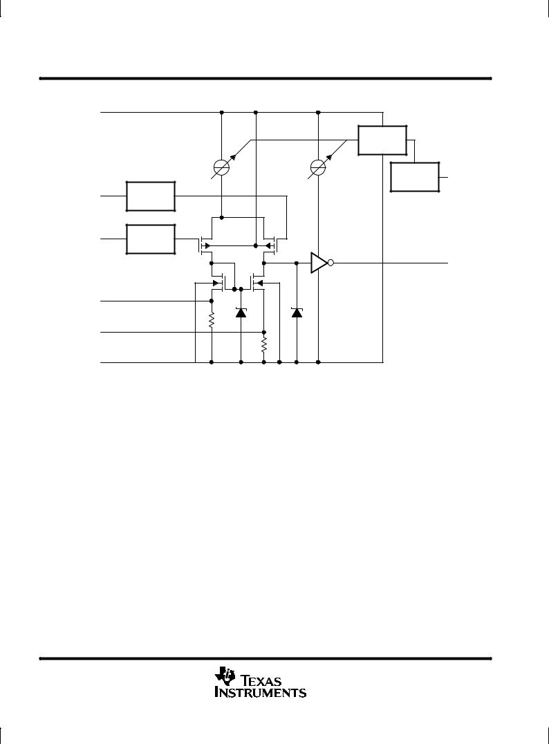
schematic |
|
|
|
|
|
VDD |
7 |
|
|
|
|
|
|
|
|
|
|
|
|
|
Current |
|
|
|
|
|
Control |
|
|
|
|
|
ESD- |
8 |
BIAS |
|
|
|
Protective |
||
|
|
|
|
SELECT |
|
|
|
ESD- |
Network |
|
|
|
3 |
|
|
||
|
|
|
|
||
IN + |
Protective |
|
|
|
|
|
|
|
|
||
|
|
Network |
|
|
|
|
2 |
ESD- |
|
|
|
IN ± |
Protective |
|
|
|
|
|
|
|
|
||
|
|
Network |
|
|
|
|
|
|
|
6 |
OUT |
|
|
|
|
|
|
OFFSET |
1 |
|
|
|
|
|
|
|
|
|
|
N1 |
|
|
|
|
|
OFFSET |
5 |
|
|
|
|
N2 |
|
|
|
|
|
VDD ± /GND |
4 |
|
|
|
|
|
|
|
|
|
|
2 |
POST OFFICE BOX 655303 •DALLAS, TEXAS 75265 |

TLC251, TLC251A, TLC251B, TLC251Y
LinCMOS PROGRAMMABLE
LOW-POWER OPERATIONAL AMPLIFIERS
SLOS001E ± JULY 1983 ± REVISED AUGUST 1994
TLC251Y chip information
These chips, properly assembled, display characteristics similar to the TLC251C. Thermal compression or ultrasonic bonding may be used on the doped-aluminum bonding pads. Chips may be mounted with conductive epoxy or a gold-silicon preform.
BONDING PAD ASSIGNMENTS
|
|
|
|
(2) |
(1) |
(8) |
(7) |
||
|
|
|
|
|
|
||||
|
|
|
|
|
|
|
|
||
48 |
|
|
|
|
|
|
|||
|
|
(3) |
(4) |
(5) |
|
|
(6) |
||
|
|
|
|
|
|
|
|
|
|
|
|
|
|
|
|
|
|
|
|
|
|
|
|
|
|
|
|
|
|
|
|
|
|
|
|
|
55 |
|
|
|
|
|
|
|
|
|
VDD |
|||
BIAS SELECT |
(8) |
|
|
|
|
(7) |
|
|||
|
|
|
|
|
||||||
|
|
|
|
|
||||||
(3) |
|
|
|
|
|
|
|
|||
IN + |
|
|
|
|
|
|
|
|||
+ |
|
|
(6) |
OUT |
||||||
|
|
|
||||||||
(2) |
|
|
||||||||
IN ± |
± |
|
||||||||
|
|
|
|
|||||||
|
|
|
|
|||||||
(1) |
|
|
|
|
|
|||||
OFFSET N1 |
|
|
|
|
|
|
|
|
|
|
|
|
|
|
|
|
|
|
|
||
|
(5) |
|
|
|
|
(4) |
|
|||
OFFSET N2 |
|
|
|
|
|
|
||||
|
|
|
|
|
|
|
|
|
||
|
|
|
|
VDD ± /GND |
||||||
CHIP THICKNESS: 15 TYPICAL BONDING PADS: 4 × 4 MINIMUM TJMAX = 150°C
TOLERANCES ARE ± 10%.
ALL DIMENSIONS ARE IN MILS.
PIN (4) IS INTERNALLY CONNECTED TO BACKSIDE OF CHIP.
POST OFFICE BOX 655303 •DALLAS, TEXAS 75265 |
3 |
TLC251, TLC251A, TLC251B, TLC251Y
LinCMOS PROGRAMMABLE
LOW-POWER OPERATIONAL AMPLIFIERS
SLOS001E ± JULY 1983 ± REVISED AUGUST 1994
absolute maximum ratings over operating free-air temperature range (unless otherwise noted)²
Supply voltage, VDD (see Note 1) . . . . . . . . . . . . . . . . . . . . . . . . . . . . . . . . . . . . . . . |
. . . . . . . . . . . . . . . . . . . . . 18 |
V |
Differential input voltage, VID (see Note 2) . . . . . . . . . . . . . . . . . . . . . . . . . . . . . . . |
. . . . . . . . . . . . . . . . . . . . ± 18 |
V |
Input voltage range, VI (any input) . . . . . . . . . . . . . . . . . . . . . . . . . . . . . . . . . . . . . . . |
. . . . . . . . . . . . ±0.3 V to 18 |
V |
Duration of short circuit at (or below) 25°C free-air temperature (see Note 3) . |
. . . . . . . . . . . . . . . . . unlimited |
|
Continuous total dissipation . . . . . . . . . . . . . . . . . . . . . . . . . . . . . . . . . . . . . . . . . . . |
See Dissipation Rating Table |
|
Operating free-air temperature range, TA . . . . . . . . . . . . . . . . . . . . . . . . . . . . . . . . |
. . . . . . . . . . . . . . 0°C to 70°C |
|
Storage temperature range . . . . . . . . . . . . . . . . . . . . . . . . . . . . . . . . . . . . . . . . . . . . . |
. . . . . . . . . . . ±65°C to 150°C |
|
Lead temperature 1,6 mm (1/16 inch) from case for 10 seconds . . . . . . . . . . . . |
. . . . . . . . . . . . . . . . . . . 260°C |
|
²Stresses beyond those listed under ªabsolute maximum ratingsº may cause permanent damage to the device. These are stress ratings only, and functional operation of the device at these or any other conditions beyond those indicated under ªrecommended operating conditionsº is not implied. Exposure to absolute-maximum-rated conditions for extended periods may affect device reliability.
NOTES: 1. All voltage values, except differential voltages, are with respect to VDD ±/GND.
2.Differential voltages are at IN+ with respect to IN ±.
3.The output may be shorted to either supply. Temperature and/or supply voltages must be limited to ensure the maximum dissipation rating is not exceeded.
|
DISSIPATION RATING TABLE |
|
||
PACKAGE |
TA ≤ 25°C |
DERATING FACTOR |
TA = 70°C |
|
POWER RATING |
ABOVE TA = 25°C |
POWER RATING |
||
|
||||
D |
725 mW |
5.8 mW/°C |
464 mW |
|
P |
1000 mW |
8.0 mW/°C |
640 mW |
|
|
|
|
|
|
recommended operating conditions
|
|
MIN |
MAX |
|
UNIT |
|
|
|
|
|
|
Supply voltage, VDD |
|
1.4 |
16 |
|
V |
|
VDD = 1.4 V |
0 |
0.2 |
|
|
Common-mode input voltage, VIC |
VDD = 5 V |
± 0.2 |
4 |
|
V |
VDD = 10 V |
± 0.2 |
9 |
|
||
|
|
|
|||
|
VDD = 16 V |
± 0.2 |
14 |
|
|
Operating free-air temperature, TA |
|
0 |
70 |
|
°C |
Bias-select voltage |
|
See Application |
|||
|
|
Information |
|
||
|
|
|
|
||
|
|
|
|
|
|
4 |
POST OFFICE BOX 655303 •DALLAS, TEXAS 75265 |
TLC251, TLC251A, TLC251B, TLC251Y
LinCMOS PROGRAMMABLE
LOW-POWER OPERATIONAL AMPLIFIERS
SLOS001E ± JULY 1983 ± REVISED AUGUST 1994
HIGH-BIAS MODE
electrical characteristics at specified free-air temperature
|
|
|
|
TEST |
|
TLC251C, TLC251AC, TLC251BC |
|
|
|||||||||
|
PARAMETER |
|
T ² |
|
|
|
|
|
|
|
|
UNIT |
|||||
|
|
V |
DD |
= 5 V |
|
V |
DD |
= 10 V |
|
||||||||
|
|
|
|
|
|
|
|
||||||||||
|
|
|
CONDITIONS |
A |
|
|
|
|
|
|
|
||||||
|
|
|
|
|
|
|
|
|
MIN |
TYP |
MAX |
MIN |
|
TYP |
MAX |
|
|
|
|
|
|
|
|
|
|
|
|
|
|
|
|
|
|
|
|
|
|
TLC251C |
|
|
|
|
|
25°C |
|
|
1.1 |
10 |
|
|
1.1 |
10 |
|
|
|
|
|
|
|
|
|
|
|
|
|
|
|
|
|
|
|
|
|
VO |
= 1.4 V, |
Full range |
|
|
|
12 |
|
|
|
12 |
|
||||
|
|
|
|
|
|
|
|
|
|
||||||||
|
|
|
|
|
|
|
|
|
|
|
|
|
|||||
|
|
|
25°C |
|
|
0.9 |
5 |
|
|
0.9 |
5 |
|
|||||
VIO |
Input offset voltage |
TLC251AC |
VIC = 0 V, |
|
|
|
|
|
mV |
||||||||
|
|
|
|
|
|
|
|
|
|
||||||||
RS |
= 50 Ω, |
|
Full range |
|
|
|
6.5 |
|
|
|
6.5 |
||||||
|
|
|
RL = 10 kΩ |
|
|
|
|
|
|
|
|
|
|||||
|
|
TLC251BC |
25°C |
|
0.34 |
2 |
|
|
0.39 |
2 |
|
||||||
|
|
|
|
|
|
|
Full range |
|
|
|
3 |
|
|
|
3 |
|
|
|
|
|
|
|
|
|
|
|
|
|
|
|
|
|
|||
|
|
|
|
|
|
|
|
|
|
|
|
|
|
|
|
|
|
αVIO |
Average temperature coefficient of |
|
|
|
|
|
25°C to |
|
|
1.8 |
|
|
|
2 |
|
μV/°C |
|
input offset voltage |
|
|
|
|
|
70°C |
|
|
|
|
|
|
|||||
IIO |
Input offset current (see Note 4) |
VO = VDD/2, |
25°C |
|
|
0.1 |
|
|
|
0.1 |
|
pA |
|||||
|
|
|
|
|
|
|
|
|
|||||||||
V |
= V |
DD |
/2 |
° |
|
|
7 |
300 |
|
|
7 |
300 |
|||||
|
|
|
IC |
|
|
70 C |
|
|
|
|
|
||||||
IIB |
Input bias current (see Note 4) |
VO = VDD/2, |
25°C |
|
|
0.6 |
|
|
|
0.7 |
|
pA |
|||||
|
|
|
|
|
|
|
|
|
|||||||||
V |
= V |
DD |
/2 |
° |
|
|
40 |
600 |
|
|
50 |
600 |
|||||
|
|
|
IC |
|
|
70 C |
|
|
|
|
|
||||||
|
|
|
|
|
|
|
|
|
± 0.2 |
± 0.3 |
|
± 0.2 |
± 0.3 |
|
|
||
|
|
|
|
|
|
|
|
25°C |
to |
|
to |
|
to |
|
to |
|
V |
VICR |
Common-mode input voltage |
|
|
|
|
|
|
4 |
|
4.2 |
|
9 |
|
9.2 |
|
|
|
range (see Note 5) |
|
|
|
|
|
|
± 0.2 |
|
|
|
± 0.2 |
|
|
|
|
||
|
|
|
|
|
|
|
|
|
|
|
|
|
|
||||
|
|
|
|
|
|
|
|
Full range |
to |
|
|
|
to |
|
|
|
V |
|
|
|
|
|
|
|
|
|
3.5 |
|
|
|
8.5 |
|
|
|
|
|
|
|
|
|
|
|
|
|
|
|
|
|
|
|
|
|
|
|
|
|
VID |
= 100 mV, |
25°C |
3.2 |
|
3.8 |
|
8 |
|
8.5 |
|
|
|||
|
|
|
|
|
|
|
|
|
|
|
|
|
|||||
VOH |
High-level output voltage |
0°C |
3 |
|
3.8 |
|
7.8 |
|
8.5 |
|
V |
||||||
RL = 10 k |
Ω |
|
|
|
|
||||||||||||
|
|
|
|
|
70°C |
3 |
|
3.8 |
|
7.8 |
|
8.4 |
|
|
|||
|
|
|
|
|
|
|
|
|
|
|
|
|
|||||
|
|
|
|
|
|
|
|
|
|
|
|
|
|
|
|
|
|
|
|
|
VID |
= ± 100 mV, |
25°C |
|
|
0 |
50 |
|
|
0 |
50 |
|
|||
|
|
|
|
|
|
|
|
|
|
|
|
|
|||||
VOL |
Low-level output voltage |
0°C |
|
|
0 |
50 |
|
|
0 |
50 |
mV |
||||||
IOL |
= 0 |
|
|
|
|
|
|
|
|||||||||
|
|
|
|
|
|
70°C |
|
|
0 |
50 |
|
|
0 |
50 |
|
||
|
|
|
|
|
|
|
|
|
|
|
|
|
|||||
|
|
|
|
|
|
|
|
|
|
|
|
|
|
|
|
|
|
|
Large-signal differential voltage |
RL = 10 kΩ, |
25°C |
5 |
|
23 |
|
10 |
|
36 |
|
|
|||||
|
|
|
|
|
|
|
|
|
|
|
|||||||
AVD |
0°C |
4 |
|
27 |
|
7.5 |
|
42 |
|
V/mV |
|||||||
amplification |
See Note 6 |
|
|
|
|
||||||||||||
|
70°C |
4 |
|
20 |
|
7.5 |
|
32 |
|
|
|||||||
|
|
|
|
|
|
|
|
|
|
|
|
|
|||||
|
|
|
|
|
|
|
|
|
|
|
|
|
|
|
|
|
|
|
|
|
|
|
|
|
|
25°C |
65 |
|
80 |
|
65 |
|
85 |
|
|
|
|
|
|
|
|
|
|
|
|
|
|
|
|||||
CMRR |
Common-mode rejection ratio |
VIC = VICRmin |
0°C |
60 |
|
84 |
|
60 |
|
88 |
|
dB |
|||||
|
|
|
|
|
|
|
|
70°C |
60 |
|
85 |
|
60 |
|
88 |
|
|
|
|
|
|
|
|
|
|
|
|
|
|
|
|
|
|
|
|
|
Supply-voltage rejection ratio |
VDD = 5 V to 10 V, |
25°C |
65 |
|
95 |
|
65 |
|
95 |
|
|
|||||
|
|
|
|
|
|
|
|
|
|
|
|||||||
kSVR |
0°C |
60 |
|
94 |
|
60 |
|
94 |
|
dB |
|||||||
( VDD/ VIO) |
VO |
= 1.4 V |
|
|
|
|
|
||||||||||
|
|
70°C |
60 |
|
96 |
|
60 |
|
96 |
|
|
||||||
|
|
|
|
|
|
|
|
|
|
|
|
|
|||||
|
|
|
|
|
|
|
|
|
|
|
|||||||
II(SEL) |
Input current (BIAS SELECT) |
VI(SEL) = 0 |
25°C |
|
± 1.4 |
|
|
± 1.9 |
|
μA |
|||||||
|
|
|
VO = VDD/2, |
25°C |
|
|
675 |
1600 |
|
|
950 |
2000 |
|
||||
|
|
|
|
|
|
|
|
|
|
|
|
μA |
|||||
IDD |
Supply current |
VIC = VDD/2, |
0°C |
|
|
775 |
1800 |
|
1125 |
2200 |
|||||||
|
|
|
No load |
|
|
|
70°C |
|
|
575 |
1300 |
|
|
750 |
1700 |
|
|
|
|
|
|
|
|
|
|
|
|
|
|
|
|||||
|
|
|
|
|
|
|
|
|
|
|
|
|
|
|
|
|
|
² Full range is 0°C to 70°C.
NOTES: 4. The typical values of input bias current and input offset current below 5 pA were determined mathematically.
5.This range also applies to each input individually.
6.At VDD = 5 V, VO = 0.25 V to 2 V; at VDD = 10 V, VO = 1 V to 6 V.
POST OFFICE BOX 655303 •DALLAS, TEXAS 75265 |
5 |
TLC251, TLC251A, TLC251B, TLC251Y
LinCMOS PROGRAMMABLE
LOW-POWER OPERATIONAL AMPLIFIERS
SLOS001E ± JULY 1983 ± REVISED AUGUST 1994
HIGH-BIAS MODE
operating characteristics, VDD = 5 V
|
|
|
|
|
|
TLC251C, TLC251AC, |
|
|
|
||
|
PARAMETER |
|
TEST CONDITIONS |
TA |
TLC251BC |
|
UNIT |
||||
|
|
|
|
|
|||||||
|
|
|
|
|
|
MIN |
TYP |
MAX |
|
|
|
|
|
|
|
|
|
|
|
|
|
|
|
|
|
|
|
|
25°C |
|
3.6 |
|
|
|
|
|
|
|
|
|
|
|
|
|
|
|
|
|
|
|
|
VI(PP) = 1 V |
0°C |
|
4 |
|
|
|
|
SR |
Slew rate at unity gain |
RL = 10 kΩ, |
CL = 20 pF |
|
70°C |
|
3 |
|
V/μs |
||
|
|
|
|
|
|||||||
|
25°C |
|
2.9 |
|
|||||||
|
|
|
|
|
|
|
|
|
|
||
|
|
|
|
|
|
|
|
|
|
|
|
|
|
|
|
VI(PP) = 2.5 V |
0°C |
|
3.1 |
|
|
|
|
|
|
|
|
|
70°C |
|
2.5 |
|
|
|
|
|
|
|
|
|
|
|
|
|
|
|
|
|
|
|
|
|
|
|
|
|
|
||
Vn |
Equivalent input noise voltage |
f = 1 kHz, |
RS = 20 Ω |
|
25°C |
|
25 |
|
nV/√ |
Hz |
|
|
|
|
|
|
25°C |
|
320 |
|
|
|
|
|
|
|
|
RL = 10 kΩ |
|
|
|
|
|
||
BOM |
Maximum output-swing bandwidth |
VO = VOH, |
CL = 20 pF, |
0°C |
|
340 |
|
kHz |
|||
|
|
|
|
|
70°C |
|
260 |
|
|
|
|
|
|
|
|
|
|
|
|
|
|
|
|
|
|
|
|
|
25°C |
|
1.7 |
|
|
|
|
|
|
|
|
|
|
|
|
|
|
||
B1 |
Unity-gain bandwidth |
VI = 10 mV, |
CL = 20 pF |
|
0°C |
|
2 |
|
MHz |
||
|
|
|
|
|
70°C |
|
1.3 |
|
|
|
|
|
|
|
|
|
|
|
|
|
|
|
|
|
|
|
|
|
25°C |
|
46° |
|
|
|
|
φm |
|
|
|
|
|
|
|
|
|
|
|
Phase margin |
VI = 10 mV, |
f = B1, |
CL = 20 pF |
0°C |
|
47° |
|
|
|
|
|
|
|
|
|
|
70°C |
|
44° |
|
|
|
|
|
|
|
|
|
|
|
|
|
|
|
|
operating characteristics, VDD = 10 V
|
|
|
|
|
|
TLC251C, TLC251AC, |
|
|
|
||
|
PARAMETER |
|
TEST CONDITIONS |
TA |
TLC251BC |
|
UNIT |
||||
|
|
|
|
|
|||||||
|
|
|
|
|
|
MIN |
TYP |
MAX |
|
|
|
|
|
|
|
|
|
|
|
|
|
|
|
|
|
|
|
|
25°C |
|
5.3 |
|
|
|
|
|
|
|
|
|
|
|
|
|
|
|
|
|
|
|
|
VI(PP) = 1 V |
0°C |
|
5.9 |
|
|
|
|
SR |
Slew rate at unity gain |
RL = 10 kΩ, |
CL = 20 pF |
|
70°C |
|
4.3 |
|
V/μs |
||
|
|
|
|
|
|||||||
|
25°C |
|
4.6 |
|
|||||||
|
|
|
|
|
|
|
|
|
|
||
|
|
|
|
|
|
|
|
|
|
|
|
|
|
|
|
VI(PP) = 5.5 V |
0°C |
|
5.1 |
|
|
|
|
|
|
|
|
|
70°C |
|
3.8 |
|
|
|
|
|
|
|
|
|
|
|
|
|
|
|
|
|
|
|
|
|
|
|
|
|
|
||
Vn |
Equivalent input noise voltage |
f = 1 kHz, |
RS = 20 Ω |
|
25°C |
|
25 |
|
nV/√ |
Hz |
|
|
|
|
|
|
25°C |
|
200 |
|
|
|
|
|
|
|
|
RL = 10 kΩ |
|
|
|
|
|
||
BOM |
Maximum output-swing bandwidth |
VO = VOH, |
CL = 20 pF, |
0°C |
|
220 |
|
kHz |
|||
|
|
|
|
|
70°C |
|
140 |
|
|
|
|
|
|
|
|
|
|
|
|
|
|
|
|
|
|
|
|
|
25°C |
|
2.2 |
|
|
|
|
|
|
|
|
|
|
|
|
|
|
||
B1 |
Unity-gain bandwidth |
VI = 10 mV, |
CL = 20 pF |
|
0°C |
|
2.5 |
|
MHz |
||
|
|
|
|
|
70°C |
|
1.8 |
|
|
|
|
|
|
|
|
|
|
|
|
|
|
|
|
|
|
|
|
|
25°C |
|
49° |
|
|
|
|
φm |
|
|
|
|
|
|
|
|
|
|
|
Phase margin |
VI = 10 mV, |
f = B1, |
CL = 20 pF |
0°C |
|
50° |
|
|
|
|
|
|
|
|
|
|
70°C |
|
46° |
|
|
|
|
|
|
|
|
|
|
|
|
|
|
|
|
6 |
POST OFFICE BOX 655303 •DALLAS, TEXAS 75265 |
 Loading...