


Texas Instruments TLE2024MJB, TLE2024MJ, TLE2024MFKB, TLE2024MDW, TLE2024IN Datasheet
...
|
TLE202x, TLE202xA, TLE202xB, TLE202xY |
||||
EXCALIBUR HIGH-SPEED LOW-POWER PRECISION |
|||||
|
OPERATIONAL AMPLIFIERS |
||||
|
SLOS191 ± FEBRUARY 1997 |
||||
|
|
|
|
|
|
D Supply Current . . . 230 μA Max |
D High Open-Loop Gain . . . 6.5 V/μV |
||||
D High Unity-Gain Bandwidth . . . 2 MHz Typ |
(136 dB) Typ |
||||
D Low Offset Voltage . . . 100 μV Max |
|||||
D High Slew Rate . . . 0.45 V/μs Min |
|||||
D Supply-Current Change Over Military Temp |
D Offset Voltage Drift With Time |
||||
0.005 μV/mo Typ |
|||||
Range . . . 10 μA Typ at VCC ± = ± 15 V |
|||||
D Specified for Both 5-V Single-Supply and |
D Low Input Bias Current . . . 50 nA Max |
||||
±15-V Operation |
D Low Noise Voltage . . . 19 nV/√ |
Hz |
Typ |
||
D Phase-Reversal Protection
description
The TLE202x, TLE202xA, and TLE202xB devices are precision, high-speed, low-power operational amplifiers using a new Texas Instruments Excalibur process. These devices combine the best features of the OP21 with highly improved slew rate and unity-gain bandwidth.
The complementary bipolar Excalibur process utilizes isolated vertical pnp transistors that yield dramatic improvement in unity-gain bandwidth and slew rate over similar devices.
The addition of a bias circuit in conjunction with this process results in extremely stable parameters with both time and temperature. This means that a precision device remains a precision device even with changes in temperature and over years of use.
This combination of excellent dc performance with a common-mode input voltage range that includes the negative rail makes these devices the ideal choice for low-level signal conditioning applications in either single-supply or split-supply configurations. In addition, these devices offer phase-reversal protection circuitry that eliminates an unexpected change in output states when one of the inputs goes below the negative supply rail.
A variety of available options includes small-outline and chip-carrier versions for high-density systems applications.
The C-suffix devices are characterized for operation from 0°C to 70°C. The I-suffix devices are characterized for operation from ±40°C to 85°C. The M-suffix devices are characterized for operation over the full military temperature range of ±55°C to 125°C.
Please be aware that an important notice concerning availability, standard warranty, and use in critical applications of
Texas Instruments semiconductor products and disclaimers thereto appears at the end of this data sheet.
PRODUCTION DATA information is current as of publication date. Products conform to specifications per the terms of Texas Instruments standard warranty. Production processing does not necessarily include testing of all parameters.
Copyright 1997, Texas Instruments Incorporated
POST OFFICE BOX 655303 •DALLAS, TEXAS 75265 |
1 |

TLE202x, TLE202xA, TLE202xB, TLE202xY
EXCALIBUR HIGH-SPEED LOW-POWER PRECISION
OPERATIONAL AMPLIFIERS
SLOS191 ± FEBRUARY 1997
TLE2021 AVAILABLE OPTIONS
|
|
|
|
PACKAGED DEVICES |
|
|
CHIP |
||
|
VIOmax |
|
|
|
|
|
|
||
|
SMALL |
|
CHIP |
|
|
|
|||
TA |
SSOP³ |
CERAMIC DIP |
PLASTIC DIP |
TSSOP³ |
FORM§ |
||||
AT 25°C |
OUTLINE² |
CARRIER |
|||||||
|
(DB) |
(JG) |
(P) |
(PW) |
(Y) |
||||
|
|
(D) |
(FK) |
||||||
|
|
|
|
|
|
|
|||
|
|
|
|
|
|
|
|
|
|
0°C to |
200 μV |
TLE2021ACD |
TLE2021CDBLE |
Ð |
Ð |
TLE2021ACP |
Ð |
Ð |
|
70°C |
500 μV |
TLE2021CD |
TLE2021CP |
TLE2021CPWLE |
TLE2021Y |
||||
|
|
|
|||||||
|
|
|
|
|
|
|
|
|
|
± 40°C |
200 μV |
TLE2021AID |
|
|
|
TLE2021AIP |
|
|
|
to |
Ð |
Ð |
Ð |
Ð |
Ð |
||||
500 μV |
TLE2021ID |
TLE2021IP |
|||||||
85°C |
|
|
|
|
|
||||
|
|
|
|
|
|
|
|
||
|
|
|
|
|
|
|
|
|
|
± 55°C |
100 μV |
Ð |
|
TLE2021BMFK |
TLE2021BMJG |
Ð |
|
|
|
to |
200 μV |
TLE2021AMD |
Ð |
TLE2021AMFK |
TLE2021AMJG |
TLE2021AMP |
Ð |
Ð |
|
125°C |
500 μV |
TLE2021MD |
|
TLE2021MFK |
TLE2021MJG |
TLE2021MP |
|
|
|
|
|
|
|
|
|
|
|
|
|
² The D packages are available taped and reeled. To order a taped and reeled part, add the suffix R (e.g., TLE2021CDR). ³ The DB and PW packages are only available left-end taped and reeled.
§ Chip forms are tested at 25°C only.
TLE2022 AVAILABLE OPTIONS
|
|
|
|
|
PACKAGED DEVICES |
|
|
CHIP |
||
|
VIOmax |
|
|
|
|
|
|
|||
T |
SMALL |
³ |
CHIP |
CERAMIC |
PLASTIC |
³ |
||||
FORM§ |
||||||||||
A |
AT 25°C |
OUTLINE² |
SSOP |
CARRIER |
DIP |
DIP |
TSSOP |
(Y) |
||
|
(DB) |
(PW) |
||||||||
|
|
|
(D) |
(FK) |
(JG) |
(P) |
||||
|
|
|
|
|
|
|||||
|
|
|
|
|
|
|
|
|
|
|
0°C |
150 |
μV |
TLE2022BCD |
Ð |
|
|
Ð |
Ð |
Ð |
|
to |
300 |
μ |
TLE2022ACD |
Ð |
Ð |
Ð |
TLE2022ACP |
Ð |
Ð |
|
V |
|
|
|
|
||||||
70°C |
500 |
μV |
TLE2022CD |
TLE2022CDBLE |
|
|
TLE2022CP |
TLE2022CPWLE |
TLE2022Y |
|
|
|
|
|
|
|
|
|
|
|
|
± 40°C |
150 |
μV |
TLE2022BID |
|
|
|
Ð |
|
|
|
to |
300 |
μV |
TLE2022AID |
Ð |
Ð |
Ð |
TLE2022AIP |
Ð |
Ð |
|
° |
500 |
μ |
TLE2022ID |
|
|
|
TLE2022IP |
|
|
|
85 C |
V |
|
|
|
|
|
|
|||
± 55°C |
150 |
μV |
Ð |
|
Ð |
TLE2022BMJG |
Ð |
|
|
|
to |
300 |
μV |
TLE2022AMD |
Ð |
TLE2022AMFK |
TLE2022AMJG |
TLE2022AMP |
Ð |
Ð |
|
125°C |
500 |
μV |
TLE2022MD |
|
TLE2022MFK |
TLE2022MJG |
TLE2022MP |
|
|
|
|
|
|
|
|
|
|
|
|
|
|
³The D packages are available taped and reeled. To oerder a taped and reeled part, add the suffix R (e.g., TLE2022CDR).
³The DB and PW packages are only available left-end taped and reeled.
² Chip forms are tested at 25°C only.
TLE2024 AVAILABLE OPTIONS
|
|
|
|
PACKAGED DEVICES |
|
CHIP |
||
|
VIOmax |
|
|
|
|
|||
T |
SMALL |
CHIP |
CERAMIC |
PLASTIC |
||||
FORM² |
||||||||
A |
AT 25°C |
OUTLINE |
CARRIER |
DIP |
DIP |
(Y) |
||
|
|
|
(DW) |
(FK) |
(J) |
(N) |
||
|
|
|
|
|||||
|
|
|
|
|
|
|
|
|
0°C to 70°C |
500 |
μV |
TLE2024BCDW |
|
|
TLE2024BCN |
Ð |
|
750 μV |
TLE2024ACDW |
Ð |
Ð |
TLE2024ACN |
Ð |
|||
|
1000 |
μV |
TLE2024CDW |
|
|
TLE2024CN |
TLE2024Y |
|
|
|
|
|
|
|
|
|
|
± 40°C to 85°C |
500 |
μV |
TLE2024BIDW |
|
|
TLE2024BIN |
|
|
750 μV |
TLE2024AIDW |
Ð |
Ð |
TLE2024AIN |
Ð |
|||
|
1000 |
μV |
TLE2024IDW |
|
|
TLE2024IN |
|
|
|
|
|
|
|
|
|
|
|
|
500 |
μV |
TLE2024BMDW |
TLE2024BMFK |
TLE2024BMJ |
TLE2024BMN |
|
|
± 55°C to 125°C |
750 μV |
TLE2024AMDW |
TLE2024AMFK |
TLE2024AMJ |
TLE2024AMN |
Ð |
||
|
1000 |
μV |
TLE2024MDW |
TLE2024MFK |
TLE2024MJ |
TLE2024MN |
|
|
|
|
|
|
|
|
|
|
|
² Chip forms are tested at 25°C only.
2 |
POST OFFICE BOX 655303 •DALLAS, TEXAS 75265 |
TLE202x, TLE202xA, TLE202xB, TLE202xY
EXCALIBUR HIGH-SPEED LOW-POWER PRECISION
OPERATIONAL AMPLIFIERS
SLOS191 ± FEBRUARY 1997
description (continued)
|
TLE2021 |
|
|
TLE2021 |
|
|||
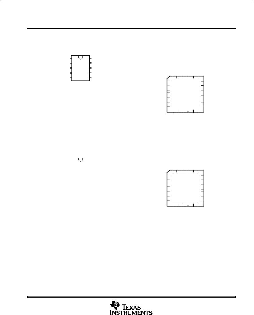
D, DB, JG, P, OR PW PACKAGE |
|
|
||||||
FK PACKAGE |
|
|||||||
|
(TOP VIEW) |
|
|
(TOP VIEW) |
|
|||
OFFSET N1 |
1 |
8 |
NC |
|
N1 |
|
|
|
NC |
OFFSET |
NC |
NC NC |
|
||||
IN ± |
2 |
7 |
VCC + |
|
||||
|
|
|
|
|
||||
IN + |
3 |
6 |
OUT |
|
|
|
|
|
VCC ±/GND |
4 |
5 |
OFFSET N2 |
|
|
|
|
|
|
|
|
NC |
3 |
2 |
1 |
20 19 |
NC |
|
|
|
4 |
|
|
18 |
||
|
|
|
IN ± |
5 |
|
|
17 |
VCC + |
|
|
|
NC |
6 |
|
|
16 |
NC |
|
|
|
IN + |
7 |
|
|
15 |
OUT |
|
|
|
NC |
8 |
|
|
14 |
NC |
|
|
|
|
9 |
10 11 12 13 |
|
||
|
|
|
|
NC |
GND |
NC |
N2 NC |
|
|
|
|
|
|
V |
|
OFFSET |
|
|
|
|
|
|
/ |
|
|
|
|
|
|
|
|
CC± |
|
|
|
NC ± No internal connection |
|
|
|
|
|
|
||
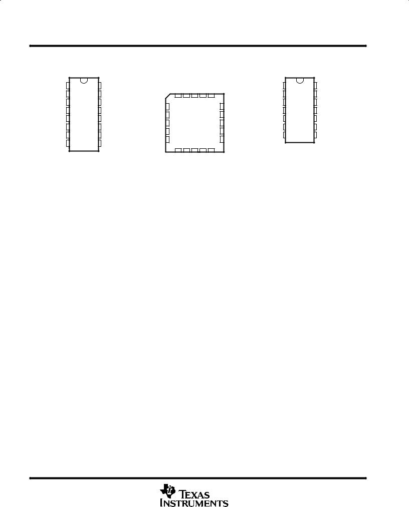
D, DB, JG, P, OR PW PACKAGE |
FK PACKAGE |
|
||||||
|
(TOP VIEW) |
|
|
(TOP VIEW) |
|
|||
1OUT |
|
1 |
8 |
|
VCC + |
|
|
||||
1IN ± |
|
|
|
|
|
|
2 |
7 |
|
2OUT |
|
1IN + |
|
3 |
6 |
|
2IN ± |
|
|
||||
VCC ±/GND |
|
4 |
5 |
|
2IN + |
|
|
||||
|
|
|
|
|
|
|
|
|
|
|
|
NC ± No internal connection
|
NC |
1OUT |
NC |
V |
NC |
|
|
|
|
|
CC+ |
|
|
NC |
3 |
2 |
1 |
20 19 |
NC |
|
4 |
|
|
|
18 |
||
1IN ± |
5 |
|
|
|
17 |
2OUT |
NC |
6 |
|
|
|
16 |
NC |
1IN + |
7 |
|
|
|
15 |
2IN ± |
NC |
8 |
|
|
|
14 |
NC |
|
9 |
10 11 12 13 |
|
|||
|
NC |
/GND |
NC |
2IN + |
NC |
|
|
|
CC ± |
|
|
|
|
|
|
V |
|
|
|
|
POST OFFICE BOX 655303 •DALLAS, TEXAS 75265 |
3 |
TLE202x, TLE202xA, TLE202xB, TLE202xY
EXCALIBUR HIGH-SPEED LOW-POWER PRECISION
OPERATIONAL AMPLIFIERS
SLOS191 ± FEBRUARY 1997 |
|
|
|
|
|
|
|
|
|
|
|
|
|
||
|
DW PACKAGE |
|
|
|
FK PACKAGE |
|
J OR N PACKAGE |
||||||||
|
(TOP VIEW) |
|
|
|
(TOP VIEW) |
|
|
(TOP VIEW) |
|
||||||
1OUT |
1 |
16 |
4OUT |
|
|
1IN ± |
1OUT |
NC |
4OUT |
4IN ± |
|
1OUT |
1 |
14 |
4OUT |
1IN ± |
2 |
15 |
4IN ± |
|
|
|
1IN± |
2 |
13 |
4IN± |
|||||
|
|
|
|
|
|
|
|
||||||||
1IN + |
3 |
14 |
4IN + |
1IN + |
4 |
3 |
2 |
1 |
20 19 |
4IN + |
1IN+ |
3 |
12 |
4IN+ |
|
VCC + |
4 |
13 |
VCC ±/GND |
|
|
|
|
18 |
VCC + |
4 |
11 |
VCC ±/GND |
|||
NC |
5 |
|
|
|
|
17 |
NC |
||||||||
2IN + |
5 |
12 |
3IN + |
|
|
|
|
2IN+ |
5 |
10 |
3IN+ |
||||
VCC + |
6 |
|
|
|
|
16 |
VCC ±/GND |
||||||||
2IN ± |
6 |
11 |
3IN ± |
|
|
|
|
2IN± |
6 |
9 |
3IN± |
||||
2OUT |
7 |
10 |
3OUT |
NC |
7 |
|
|
|
|
15 |
NC |
2OUT |
7 |
8 |
3OUT |
2IN + |
8 |
|
|
|
|
14 |
3IN + |
||||||||
NC |
8 |
9 |
NC |
9 |
|
|
|
|
|
|
|
||||
|
|
10 11 12 13 |
|
|
|
|
|
||||||||
|
|
|
|
|
|
2IN ± |
2OUT |
NC |
3OUT |
3IN ± |
|
|
|
|
|
NC ± No internal connection
4 |
POST OFFICE BOX 655303 •DALLAS, TEXAS 75265 |

TLE202x, TLE202xA, TLE202xB, TLE202xY
EXCALIBUR HIGH-SPEED LOW-POWER PRECISION
OPERATIONAL AMPLIFIERS
SLOS191 ± FEBRUARY 1997
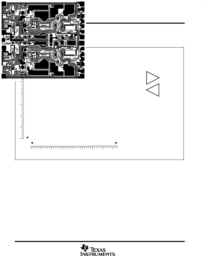
TLE2021Y chip information
This chip, when properly assembled, display characteristics similar to the TLE2021. Thermal compression or ultrasonic bonding may be used on the doped-aluminum bonding pads. This chip may be mounted with conductive epoxy or a gold-silicon preform.
BONDING PAD ASSIGNMENTS
|
|
|
|
(7) |
(6) |
(5) |
|
|
|
|
|
|
|
||
78 |
|
|
|
|
|||
|
|
|
|
|
|
(4) |
|
|
|
(1) |
|
|
|
||
|
|
|
|
|
(2) |
(3) |
|
|
|
|
|
|
|
|
|
|
|
|
|
|
|
|
|
|
|
|
|
|
|
54 |
|
|
|
|
|
|
|
|
|
|
|
(1) |
|
|
VCC+ |
|
|
|||
OFFSET N1 |
|
|
|
(7) |
|
|
|
|||
|
|
|
|
|||||||
(3) |
|
|
|
|
|
|
|
|
||
IN + |
|
|
|
|
|
|
|
|
||
|
+ |
|
|
|
(6) |
|||||
|
|
|
|
|
|
|||||
|
|
|
|
|
|
|
|
|
||
IN ± |
(2) |
|
± |
|
|
|
|
OUT |
||
|
|
|
|
|
||||||
|
|
|
|
|
|
|||||
|
|
|
|
|
|
|
|
|||
(5) |
|
|
|
|||||||
|
|
|
|
|
|
|||||
OFFSET N2 |
|
|
|
|
|
|
|
|
||
|
|
|
|
|
|
|
|
|||
|
|
|
|
|
|
(4) |
|
|
|
|
|
|
|
|
|
|
|
|
|
||
|
|
|
|
|
|
|
|
|
||
|
|
|
VCC ± /GND |
|
|
|||||
CHIP THICKNESS: 15 MILS TYPICAL
BONDING PADS: 4 × 4 MILS MINIMUM
TJmax= 150°C
TOLERANCES ARE ± 10%.
ALL DIMENSIONS ARE IN MILS.
PIN (4) IS INTERNALLY CONNECTED TO BACKSIDE OF CHIP.
POST OFFICE BOX 655303 •DALLAS, TEXAS 75265 |
5 |
TLE202x, TLE202xA, TLE202xB, TLE202xY
EXCALIBUR HIGH-SPEED LOW-POWER PRECISION
OPERATIONAL AMPLIFIERS
SLOS191 ± FEBRUARY 1997
TLE2022Y chip information
This chip, when properly assembled, displays characteristics similar to TLE2022. Thermal compression or ultrasonic bonding may be used on the doped-aluminum bonding pads. This chip may be mounted with conductive epoxy or a gold-silicon preform.
BONDING PAD ASSIGNMENTS
|
|
|
|
(7) |
(6) |
|
|
|
|
|
|
|
|
|
|
|
|
||
|
|
|
|
|
|
|
|
|
|
|
|
VCC+ |
|
|
|
|
|||
|
|
|
|
|
|
|
|
|
(3) |
|
|
|
(8) |
|
|
|
|
|
|
|
|
|
|
|
|
|
|
IN + |
+ |
|
|
|
|
|
|
|
|||
|
|
|
|
|
|
|
|
|
|
|
|
|
(1) |
|
OUT |
||||
|
|
|
|
|
|
|
|
|
|
|
|||||||||
|
|
|
|
|
|
|
|
|
|
|
|
|
|
||||||
|
|
|
|
|
|
|
|
|
|
|
|
|
|
|
|
|
|||
|
|
|
|
|
|
|
|
IN ± |
(2) |
± |
|
|
|
|
|
|
|||
|
|
|
|
|
|
|
|
|
|
|
|
|
|
||||||
|
|
|
|
|
|
|
|
|
|
|
|
|
|
|
|||||
|
|
|
|
|
|
|
|
|
|
|
|
|
(5) |
|
|
||||
|
|
|
|
|
|
|
|
|
|
|
|
||||||||
|
|
|
|
|
|
|
|
|
|
|
+ |
|
|
IN + |
|||||
|
|
|
|
|
(8) |
|
|
OUT |
(7) |
|
|
|
|
||||||
|
|
|
|
|
|
|
|
|
|
|
|||||||||
|
|
|
|
|
|
|
|
|
|
|
|
|
|
|
|||||
|
|
(5) |
|
|
|
|
|
± |
|
(6) |
|
IN ± |
|||||||
|
|
|
|
|
|
|
|||||||||||||
|
|
|
|
|
|
|
|
|
|
|
|
|
|
|
|||||
|
|
|
|
|
|
|
|
|
|
|
|
|
|||||||
|
|
|
|
|
|
|
|
|
|
|
|
(4) |
|
|
|
|
|
||
80 |
|
|
(4) |
|
|
|
|
|
|
|
|
|
|
|
|||||
|
(1) |
|
|
|
|
VCC ± |
|
|
|
|
|||||||||
|
|
|
|
|
|
|
|
|
|
|
|
|
|||||||
|
|
|
|
|
|
|
|
|
|
|
|
|
|||||||
|
|
|
|
|
|
|
|
|
|
|
|
|
|
|
|||||
|
|
|
|
CHIP THICKNESS: 15 MILS TYPICAL |
|||||||||||||||
|
|
|
|
|
|
|
|
||||||||||||
|
|
|
|
|
|
|
|
BONDING PADS: 4 × 4 MILS MINIMUM |
|||||||||||
|
|
|
|
|
|
|
|
TJmax = 150°C |
|
|
|
|
|
|
|
|
|
||
|
|
|
|
|
|
|
|
TOLERANCES ARE ± 10%. |
|
|
|
|
|||||||
|
|
|
|
|
|
|
|
ALL DIMENSIONS ARE IN MILS. |
|
||||||||||
|
|
(2) |
(3) |
PIN (4) IS INTERNALLY CONNECTED |
|||||||||||||||
|
|
|
|
|
|
|
|
||||||||||||
|
|
|
|
|
|
|
|
TO BACKSIDE OF CHIP. |
|
|
|
|
|||||||
|
|
|
|
|
|
|
|
|
|
|
|
||||||||
|
|
|
|
|
|
86 |
|
|
|
|
|
|
|
|
|
|
|
|
|
|
|
|
|
|
|
|
|
|
|
|
|
|
|
|
|
|
|
|
|
|
|
|
|
|
|
|
|
|
|
|
|
|
|
|
|
|
|
|
|
6 |
POST OFFICE BOX 655303 •DALLAS, TEXAS 75265 |

TLE202x, TLE202xA, TLE202xB, TLE202xY
EXCALIBUR HIGH-SPEED LOW-POWER PRECISION
OPERATIONAL AMPLIFIERS
SLOS191 ± FEBRUARY 1997
TLE2024Y chip information
This chip, when properly assembled, displays characteristics similar to the TLE2024. Thermal compression or ultrasonic bonding may be used on the doped aluminum-bonding pads. This chip may be mounted with conductive epoxy or a gold-silicon preform.
BONDING PAD ASSIGNMENTS
 100
100
140
|
|
|
VCC + |
|
|
|
|
||
|
(3) |
|
|
|
(4) |
|
|
|
|
1IN + |
+ |
|
|
|
|
|
|
||
|
|
|
(1) |
|
|
1OUT |
|||
|
|
|
|||||||
|
|
|
|
||||||
|
|
|
|
|
|
|
|
||
1IN ± |
(2) |
± |
|
|
|
|
|
||
|
|
|
|
||||||
|
|
|
|
|
|
||||
|
|
|
(5) |
|
|
|
|||
|
|
|
|
||||||
|
|
+ |
|
|
2IN + |
||||
2OUT |
(7) |
|
|
|
|||||
|
|
|
|||||||
|
|
|
|
|
|
|
|||
|
|
|
|
|
(6) |
|
|
|
|
|
± |
|
|
2IN ± |
|||||
|
|
|
|
||||||
2IN + |
(10) |
|
|
|
|||||
|
|
|
|||||||
+ |
|
|
|
|
|
|
|||
|
|
|
(8) |
|
|
3OUT |
|||
|
|
|
|
|
|||||
|
|
|
|
|
|
|
|
||
3IN ± |
(9) |
± |
|
|
|
|
|
||
|
|
|
|
|
|||||
|
|
|
|
|
|
||||
|
|
|
(12) |
|
|
||||
|
|
|
|
|
|||||
|
|
+ |
|
4IN + |
|||||
4OUT |
(14) |
|
|
|
|||||
|
|
|
|||||||
|
|
|
|
|
|
|
|
||
|
|
|
± |
(13) |
|
4IN ± |
|||
|
|
|
|
||||||
|
|
|
|
|
|||||
|
|
|
|
|
|
|
|||
|
|
|
(11) |
|
|
|
|
||
|
VCC ± /GND |
|
|
|
|
||||
CHIP THICKNESS: 15 MILS TYPICAL BONDING PADS: 4 × 4 MILS MINIMUM TJmax = 150°C
TOLERANCES ARE ± 10%.
ALL DIMENSIONS ARE IN MILS.
PIN (11) IS INTERNALLY CONNECTED TO BACKSIDE OF CHIP.
POST OFFICE BOX 655303 •DALLAS, TEXAS 75265 |
7 |
TLE202x, TLE202xA, TLE202xB, TLE202xY
EXCALIBUR HIGH-SPEED LOW-POWER PRECISION
OPERATIONAL AMPLIFIERS
SLOS191 ± FEBRUARY 1997
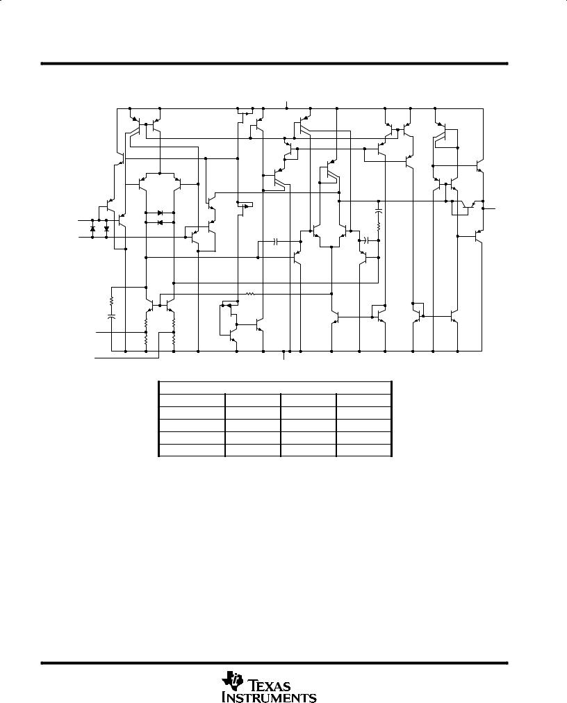
equivalent schematic (each amplifier)
|
|
|
|
|
VCC+ |
|
|
|
|
|
|
|
|
|
Q13 |
|
Q22 |
|
|
|
|
|
Q3 |
Q7 |
|
Q17 |
|
Q28 |
Q31 |
Q35 |
|
|
|
|
|
|
|
|
|
|
|||
|
|
|
|
Q19 |
|
Q29 |
|
|
|
|
Q1 |
|
|
|
|
|
Q24 |
Q32 |
Q39 |
||
|
|
|
|
|
|
|||||
|
|
|
|
|
|
|
|
|||
|
Q5 |
Q8 |
|
|
Q20 |
|
|
|
|
Q36 |
|
|
|
|
|
|
|
Q34 |
|||
Q2 |
|
D3 |
Q11 |
|
|
|
|
|
Q38 |
|
|
|
|
C4 |
|
|
|
||||
IN ± |
|
|
|
|
|
|
|
|
OUT |
|
Q4 |
|
|
Q14 |
|
|
|
|
|
||
|
|
|
|
|
|
|
|
|||
|
|
D4 |
|
Q12 |
|
Q23 Q25 |
R7 |
|
|
|
IN + |
|
|
Q10 |
C2 |
|
|
|
|
Q40 |
|
D1 D2 |
|
|
|
|
|
|
C3 |
|
|
|
|
|
|
|
|
|
|
|
|
|
|
|
|
|
|
|
|
Q21 |
Q27 |
|
|
|
|
|
|
|
R6 |
|
|
|
|
|
|
R1 |
Q6 |
Q9 |
|
Q15 |
|
|
|
|
|
|
|
|
|
|
|
|
|
|
|||
C1 |
|
|
|
|
Q26 |
Q30 |
Q33 |
|
Q37 |
|
R2 |
R4 |
|
Q18 |
|
|
|||||
OFFSET N1 |
|
|
|
|
|
|
|
|||
|
|
|
Q16 |
|
|
|
|
|
|
|
(see Note A) |
R3 |
R5 |
|
|
|
|
|
|
|
|
|
|
|
|
|
|
|
|
|||
|
|
|
|
|
|
|
|
|
||
OFFSET N2 |
|
|
|
|
|
|
|
|
|
|
(see Note A) |
|
|
|
VCC ± /GND |
|
|
|
|
||
|
|
|
ACTUAL DEVICE COMPONENT COUNT |
|
|
|
|
|||
|
|
COMPONENT |
TLE2021 |
TLE2022 |
TLE2024 |
|
|
|
||
|
|
Transistors |
|
40 |
|
80 |
160 |
|
|
|
|
|
Resistors |
|
7 |
|
14 |
28 |
|
|
|
|
|
Diodes |
|
4 |
|
8 |
16 |
|
|
|
|
|
Capacitors |
|
4 |
|
8 |
16 |
|
|
|
8 |
POST OFFICE BOX 655303 •DALLAS, TEXAS 75265 |

TLE202x, TLE202xA, TLE202xB, TLE202xY
EXCALIBUR HIGH-SPEED LOW-POWER PRECISION
OPERATIONAL AMPLIFIERS
SLOS191 ± FEBRUARY 1997
absolute maximum ratings over operating free-air temperature range (unless otherwise noted)²
Supply voltage, VCC+ (see Note 1) . . . . . . . . . . . . . . . . . . . . . . . . . . . . . . . . . . . . . |
. . . . . . . . . . . |
. . . . . . . . . . 20 V |
Supply voltage, VCC± (see Note 1) . . . . . . . . . . . . . . . . . . . . . . . . . . . . . . . . . . . . . . |
. . . . . . . . . . . |
. . . . . . . . . ±20 V |
Differential input voltage, VID (see Note 2) . . . . . . . . . . . . . . . . . . . . . . . . . . . . . . . |
. . . . . . . . . . . . |
. . . . . . . ± 0.6 V |
Input voltage range, VI (any input, see Note 1) . . . . . . . . . . . . . . . . . . . . . . . . . . . . |
. . . . . . . . . . . . |
. . . . . . . . ±VCC |
Input current, II (each input) . . . . . . . . . . . . . . . . . . . . . . . . . . . . . . . . . . . . . . . . . . . . |
. . . . . . . . . . . . |
. . . . . . . ±1 mA |
Output current, IO (each output): TLE2021 . . . . . . . . . . . . . . . . . . . . . . . . . . . . . . . |
. . . . . . . . . . . . |
. . . . . . ± 20 mA |
TLE2022 . . . . . . . . . . . . . . . . . . . . . . . . . . . . . . . |
. . . . . . . . . . . . |
. . . . . . ± 30 mA |
TLE2024 . . . . . . . . . . . . . . . . . . . . . . . . . . . . . . . |
. . . . . . . . . . . . |
. . . . . . ± 40 mA |
Total current into VCC+ . . . . . . . . . . . . . . . . . . . . . . . . . . . . . . . . . . . . . . . . . . . . . . . . |
. . . . . . . . . . . . |
. . . . . . . 80 mA |
Total current out of VCC± . . . . . . . . . . . . . . . . . . . . . . . . . . . . . . . . . . . . . . . . . . . . . . |
. . . . . . . . . . . . |
. . . . . . . 80 mA |
Duration of short-circuit current at (or below) 25°C (see Note 3) . . . . . . . . . . . . . |
. . . . . . . . . . . . |
. . . . . unlimited |
Continuous total power dissipation . . . . . . . . . . . . . . . . . . . . . . . . . . . . . . . . . . . . . |
See Dissipation Rating Table |
|
Operating free-air temperature range, TA: C suffix . . . . . . . . . . . . . . . . . . . . . . . . . |
. . . . . . . . . . . . |
. . 0°C to 70°C |
I suffix . . . . . . . . . . . . . . . . . . . . . . . . . . |
. . . . . . . . . . . . |
±40°C to 85°C |
M suffix . . . . . . . . . . . . . . . . . . . . . . . . . |
. . . . . . . . . . . |
±55°C to 125°C |
Storage temperature range, Tstg . . . . . . . . . . . . . . . . . . . . . . . . . . . . . . . . . . . . . . . . |
. . . . . . . . . . . |
±65°C to 150°C |
Case temperature for 60 seconds, TC: FK package . . . . . . . . . . . . . . . . . . . . . . . |
. . . . . . . . . . . . |
. . . . . . . 260°C |
Lead temperature 1,6 mm (1/16 inch) from case for 10 seconds: D, DP, P, or PW package . |
. . . . . . . 260°C |
|
Lead temperature 1,6 mm (1/16 inch) from case for 60 seconds: JG package . |
. . . . . . . . . . . . |
. . . . . . . 300°C |
²Stresses beyond those listed under ªabsolute maximum ratingsº may cause permanent damage to the device. These are stress ratings only, and functional operation of the device at these or any other conditions beyond those indicated under ªrecommended operating conditionsº is not
implied. Exposure to absolute-maximum-rated conditions for extended periods may affect device reliability.
NOTES: 1. All voltage values, except differential voltages, are with respect to the midpoint between VCC +, and VCC ±.
2.Differential voltages are at IN+ with respect to IN ±. Excessive current flows if a differential input voltage in excess of approximately
± 600 mV is applied between the inputs unless some limiting resistance is used.
3.The output may be shorted to either supply. Temperature and/or supply voltages must be limited to ensure that the maximum dissipation rating is not exceeded.
DISSIPATION RATING TABLE
PACKAGE |
TA ≤ 25°C |
DERATING FACTOR |
TA = 70°C |
TA = 85°C |
TA = 125°C |
|
POWER RATING |
ABOVE TA = 25°C |
POWER RATING |
POWER RATING |
POWER RATING |
||
|
||||||
D±8 |
725 mW |
5.8 mW/°C |
464 mW |
377 mW |
145 mW |
|
DB±8 |
525 mW |
4.2 mW/°C |
336 mW |
Ð |
Ð |
|
DW±16 |
1025 mW |
8.2 mW/°C |
656 mW |
533 mW |
205 mW |
|
FK |
1375 mW |
11.0 mW/°C |
880 mW |
715 mW |
275 mW |
|
J±14 |
1375 mW |
11.0 mW/°C |
880 mW |
715 mW |
275 mW |
|
JG±8 |
1050 mW |
8.4 mW/°C |
672 mW |
546 mW |
210 mW |
|
N±14 |
1150 mW |
9.2 mW/°C |
736 mW |
598 mW |
230 mW |
|
P±8 |
1000 mW |
8.0 mW/°C |
640 mW |
520 mW |
200 mW |
|
PW±8 |
525 mW |
4.2 mW/°C |
336 mW |
Ð |
Ð |
recommended operating conditions
|
|
|
C SUFFIX |
I SUFFIX |
M SUFFIX |
UNIT |
|
|||
|
|
|
|
|
|
|
|
|
|
|
|
|
|
MIN |
MAX |
MIN |
MAX |
MIN |
MAX |
|
|
|
|
|
|
|
||||||
|
|
|
|
|
|
|
|
|
|
|
Supply voltage, VCC |
|
|
± 2 |
± 20 |
± 2 |
± 20 |
± 2 |
± 20 |
V |
|
Common-mode input voltage, VIC |
VCC = ± 5 V |
0 |
3.5 |
0 |
3.2 |
0 |
3.2 |
V |
|
|
VCC ± = |
± 15 V |
±15 |
13.5 |
±15 |
13.2 |
±15 |
13.2 |
|
||
|
|
|
||||||||
Operating free-air temperature, TA |
|
|
0 |
70 |
± 40 |
85 |
± 55 |
125 |
°C |
|
|
|
|
|
|
|
|
|
|
|
|
|
|
|
|
|
|
|
|
|
|
|
POST OFFICE BOX 655303 •DALLAS, TEXAS 75265 |
9 |

10
75265 TEXAS DALLAS, •655303 BOX OFFICE POST
TLE2021 electrical characteristics at specified free-air temperature, VCC = 5 V (unless otherwise noted)
|
PARAMETER |
TEST CONDITIONS |
T ² |
TLE2021C |
|
TLE2021AC |
|
TLE2021BC |
|
UNIT |
|||
|
|
|
|
|
|
|
|
|
|
||||
|
|
|
|
|
|
|
|
|
|
||||
|
|
|
A |
MIN |
TYP |
MAX |
MIN |
TYP |
MAX |
MIN |
TYP |
MAX |
|
|
|
|
|
|
|||||||||
VIO |
Input offset voltage |
|
25°C |
|
120 |
600 |
|
100 |
300 |
|
80 |
200 |
μV |
|
|
|
|
|
|
|
|
|
|
|
|||
|
Full range |
|
|
850 |
|
|
600 |
|
|
300 |
|||
|
|
|
|
|
|
|
|
|
|
||||
|
|
|
|
|
|
|
|
|
|
|
|
|
|
αVIO |
Temperature coefficient of |
|
Full range |
|
2 |
|
|
2 |
|
|
2 |
|
μV/°C |
input offset voltage |
|
|
|
|
|
|
|
||||||
|
|
|
|
|
|
|
|
|
|
|
|
|
|
|
|
|
|
|
|
|
|
|
|
|
|
|
|
|
Input offset voltage long-term drift |
|
25°C |
|
0.005 |
|
|
0.005 |
|
|
0.005 |
|
μV/mo |
|
(see Note 4) |
VIC = 0, RS = 50 Ω |
|
|
|
|
|
|
|||||
|
|
|
|
|
|
|
|
|
|
|
|
||
IIO |
Input offset current |
|
25°C |
|
0.2 |
6 |
|
0.2 |
6 |
|
0.2 |
6 |
nA |
|
|
|
|
|
|
|
|
|
|
|
|||
|
Full range |
|
|
10 |
|
|
10 |
|
|
10 |
|||
|
|
|
|
|
|
|
|
|
|
||||
|
|
|
|
|
|
|
|
|
|
|
|
|
|
IIB |
Input bias current |
|
25°C |
|
25 |
70 |
|
25 |
70 |
|
25 |
70 |
nA |
|
|
|
|
|
|
|
|
|
|
|
|||
|
Full range |
|
|
90 |
|
|
90 |
|
|
90 |
|||
|
|
|
|
|
|
|
|
|
|
||||
|
|
|
|
|
|
|
|
|
|
|
|
|
|
|
|
|
|
0 |
± 0.3 |
|
0 |
± 0.3 |
|
0 |
± 0.3 |
|
|
|
|
|
25°C |
to |
to |
|
to |
to |
|
to |
to |
|
|
VICR |
Common-mode input voltage range |
RS = 50 Ω |
|
3.5 |
4 |
|
3.5 |
4 |
|
3.5 |
4 |
|
V |
|
|
|
|
|
|
|
|
|
|
||||
|
0 |
|
|
0 |
|
|
0 |
|
|
||||
|
|
|
|
|
|
|
|
|
|
|
|||
|
|
|
Full range |
to |
|
|
to |
|
|
to |
|
|
|
|
|
|
|
3.5 |
|
|
3.5 |
|
|
3.5 |
|
|
|
|
|
|
|
|
|
|
|
|
|
|
|
|
|
VOH |
High-level output voltage |
|
25°C |
4 |
4.3 |
|
4 |
4.3 |
|
4 |
4.3 |
|
V |
|
|
|
|
|
|
|
|
|
|
|
|||
RL= 10 kΩ |
Full range |
3.9 |
|
|
3.9 |
|
|
3.9 |
|
|
|||
|
|
|
|
|
|
|
|
|
|||||
|
|
|
|
|
|
|
|
|
|
|
|
|
|
VOL |
Low-level output voltage |
25°C |
|
0.7 |
0.8 |
|
0.7 |
0.8 |
|
0.7 |
0.8 |
V |
|
|
|
|
|
||||||||||
|
|
|
|
|
|
|
|
|
|
|
|||
|
Full range |
|
|
0.85 |
|
|
0.85 |
|
|
0.85 |
|||
|
|
|
|
|
|
|
|
|
|
||||
|
|
|
|
|
|
|
|
|
|
|
|
|
|
AVD |
Large-signal differential |
VO = 1.4 V to 4 V, |
25°C |
0.3 |
1.5 |
|
0.3 |
1.5 |
|
0.3 |
1.5 |
|
V/μV |
|
|
|
|
|
|
|
|
|
|
||||
voltage amplification |
RL = 10 kΩ |
Full range |
0.3 |
|
|
0.3 |
|
|
0.3 |
|
|
||
|
|
|
|
|
|
|
|
||||||
CMRR |
Common-mode rejection ratio |
VIC = VICRmin, |
25°C |
85 |
110 |
|
85 |
110 |
|
85 |
110 |
|
dB |
|
|
|
|
|
|
|
|
|
|
||||
RS = 50 Ω |
Full range |
80 |
|
|
80 |
|
|
80 |
|
|
|||
|
|
|
|
|
|
|
|
|
|||||
kSVR |
Supply-voltage rejection ratio |
VCC = 5 V to 30 V |
25°C |
105 |
120 |
|
105 |
120 |
|
105 |
120 |
|
dB |
( VCC / VIO) |
Full range |
100 |
|
|
100 |
|
|
100 |
|
|
|||
|
|
|
|
|
|
|
|
|
|||||
ICC |
Supply current |
|
25°C |
|
170 |
230 |
|
170 |
230 |
|
170 |
230 |
μA |
VO = 2.5 V, |
|
|
|
|
|
|
|
|
|
|
|||
Full range |
|
|
230 |
|
|
230 |
|
|
230 |
||||
|
|
|
|
|
|
|
|
|
|||||
ICC |
Supply-current change over |
No load |
Full range |
|
5 |
|
|
5 |
|
|
5 |
|
μA |
|
|
|
|
|
|
|
|||||||
operating temperature range |
|
|
|
|
|
|
|
||||||
|
|
|
|
|
|
|
|
|
|
|
|
|
|
|
|
|
|
|
|
|
|
|
|
|
|
|
|
² Full range is 0°C to 70°C.
NOTE 4: Typical values are based on the input offset voltage shift observed through 168 hours of operating life test at TA = 150°C extrapolated to TA = 25°C using the Arrhenius equation and assuming an activation energy of 0.96 eV.
TLE202xY TLE202xB, TLE202xA, TLE202x, PRECISION POWER-LOW SPEED-HIGH EXCALIBUR AMPLIFIERS OPERATIONAL 1997 FEBRUARY ± SLOS191 |
7±11±94 Date: Release Template |
75265 TEXAS DALLAS, •655303 BOX OFFICE POST
11
TLE2021 electrical characteristics at specified free-air temperature, VCC = ±15 V (unless otherwise noted)
|
PARAMETER |
TEST CONDITIONS |
T ² |
TLE2021C |
|
TLE2021AC |
|
TLE2021BC |
|
UNIT |
|||||
|
|
|
|
|
|
|
|
|
|
||||||
|
|
|
|
|
|
|
|
|
|
||||||
|
|
|
|
|
A |
MIN |
TYP |
MAX |
MIN |
TYP |
MAX |
MIN |
TYP |
MAX |
|
|
|
|
|
|
|
|
|||||||||
VIO |
Input offset voltage |
|
|
|
25°C |
|
120 |
500 |
|
80 |
200 |
|
40 |
100 |
μV |
|
|
|
|
|
|
|
|
|
|
|
|
|
|||
|
|
|
Full range |
|
|
750 |
|
|
500 |
|
|
200 |
|||
|
|
|
|
|
|
|
|
|
|
|
|
||||
|
|
|
|
|
|
|
|
|
|
|
|
|
|
|
|
αVIO |
Temperature coefficient of |
|
|
|
Full range |
|
2 |
|
|
2 |
|
|
2 |
|
μV/°C |
input offset voltage |
|
|
|
|
|
|
|
|
|
||||||
|
|
|
|
|
|
|
|
|
|
|
|
|
|
|
|
|
|
|
|
|
|
|
|
|
|
|
|
|
|
|
|
|
Input offset voltage long-term drift |
VIC = 0, |
RS = 50 |
Ω |
25°C |
|
0.006 |
|
|
0.006 |
|
|
0.006 |
|
μV/mo |
|
(see Note 4) |
|
|
|
|
|
|
||||||||
|
|
|
|
|
|
|
|
|
|
|
|
|
|||
|
|
|
|
|
|
|
|
|
|
|
|
|
|
|
|
IIO |
Input offset current |
|
|
|
25°C |
|
0.2 |
6 |
|
0.2 |
6 |
|
0.2 |
6 |
nA |
|
|
|
|
|
|
|
|
|
|
|
|
|
|||
|
|
|
Full range |
|
|
10 |
|
|
10 |
|
|
10 |
|||
|
|
|
|
|
|
|
|
|
|
|
|
||||
|
|
|
|
|
|
|
|
|
|
|
|
|
|
|
|
IIB |
Input bias current |
|
|
|
25°C |
|
25 |
70 |
|
25 |
70 |
|
25 |
70 |
nA |
|
|
|
|
|
|
|
|
|
|
|
|
|
|||
|
|
|
Full range |
|
|
90 |
|
|
90 |
|
|
90 |
|||
|
|
|
|
|
|
|
|
|
|
|
|
||||
|
|
|
|
|
|
|
|
|
|
|
|
|
|
|
|
|
|
|
|
|
|
± 15 |
± 15.3 |
|
± 15 |
± 15.3 |
|
± 15 |
± 15.3 |
|
|
|
|
|
|
|
25°C |
to |
to |
|
to |
to |
|
to |
to |
|
|
VICR |
Common-mode input voltage range |
RS = 50 Ω |
|
|
13.5 |
14 |
|
13.5 |
14 |
|
13.5 |
14 |
|
V |
|
|
|
|
|
|
|
|
|
|
|
|
|||||
|
|
± 15 |
|
|
15 |
|
|
15 |
|
|
|||||
|
|
|
|
|
|
|
|
|
|
|
|
|
|||
|
|
|
|
|
Full range |
to |
|
|
to |
|
|
to |
|
|
|
|
|
|
|
|
|
13.5 |
|
|
13.5 |
|
|
13.5 |
|
|
|
|
|
|
|
|
|
|
|
|
|
|
|
|
|
|
|
VOM+ |
Maximum positive peak |
|
|
|
25°C |
14 |
14.3 |
|
14 |
14.3 |
|
14 |
14.3 |
|
V |
output voltage swing |
RL = 10 kΩ |
|
Full range |
13.9 |
|
|
13.9 |
|
|
13.9 |
|
|
|||
|
|
|
|
|
|
|
|
|
|||||||
|
|
|
|
|
|
|
|
|
|
|
|
|
|
||
VOM ± |
Maximum negative peak |
|
25°C |
± 13.7 |
± 14.1 |
|
± 13.7 |
± 14.1 |
|
± 13.7 |
± 14.1 |
|
V |
||
|
|
|
|
|
|
||||||||||
output voltage swing |
|
|
|
Full range |
± 13.7 |
|
|
± 13.7 |
|
|
± 13.7 |
|
|
||
|
|
|
|
|
|
|
|
|
|
|
|||||
|
|
|
|
|
|
|
|
|
|
|
|
|
|
|
|
AVD |
Large-signal differential |
VO = ± 10 V, |
|
25°C |
1 |
6.5 |
|
1 |
6.5 |
|
1 |
6.5 |
|
V/μV |
|
voltage amplification |
RL = 10 kΩ |
|
Full range |
1 |
|
|
1 |
|
|
1 |
|
|
|||
|
|
|
|
|
|
|
|
|
|||||||
CMRR |
Common-mode rejection ratio |
VIC = VICR min, |
|
25°C |
100 |
115 |
|
100 |
115 |
|
100 |
115 |
|
dB |
|
|
|
|
|
|
|
|
|
|
|
|
|||||
RS = 50 Ω |
|
Full range |
96 |
|
|
96 |
|
|
96 |
|
|
||||
|
|
|
|
|
|
|
|
|
|
||||||
kSVR |
Supply-voltage rejection ratio |
VCC ± = ± 2.5 V |
|
25°C |
105 |
120 |
|
105 |
120 |
|
105 |
120 |
|
dB |
|
( VCC / VIO) |
to ± 15 V |
|
|
Full range |
100 |
|
|
100 |
|
|
100 |
|
|
||
|
|
|
|
|
|
|
|
|
|
||||||
ICC |
Supply current |
|
|
|
25°C |
|
200 |
300 |
|
200 |
300 |
|
200 |
300 |
μA |
|
|
|
|
|
|
|
|
|
|
|
|
|
|||
VO = 0, |
No load |
|
Full range |
|
|
300 |
|
|
300 |
|
|
300 |
|||
|
|
|
|
|
|
|
|
|
|
||||||
|
|
|
|
|
|
|
|
|
|
|
|
|
|
||
ICC |
Supply-current change over |
|
Full range |
|
6 |
|
|
6 |
|
|
6 |
|
μA |
||
|
|
|
|
|
|
|
|
|
|||||||
operating temperature range |
|
|
|
|
|
|
|
|
|
||||||
|
|
|
|
|
|
|
|
|
|
|
|
|
|
|
|
|
|
|
|
|
|
|
|
|
|
|
|
|
|
|
|
² Full range is 0°C to 70°C.
NOTE 4: Typical values are based on the input offset voltage shift observed through 168 hours of operating life test at TA = 150°C extrapolated to TA = 25°C using the Arrhenius equation and assuming an activation energy of 0.96 eV.
-HIGH EXCALIBUR |
TLE202x, |
PRECISION POWER-LOW SPEED AMPLIFIERS OPERATIONAL 1997 FEBRUARY ± SLOS191 |
TLE202xY TLE202xB, TLE202xA, |
12
75265 TEXAS DALLAS, •655303 BOX OFFICE POST
TLE2022 electrical characteristics at specified free-air temperature, VCC = 5 V (unless otherwise noted)
|
PARAMETER |
TEST CONDITIONS |
T ² |
TLE2022C |
|
TLE2022AC |
|
TLE2022BC |
|
UNIT |
||||
|
|
|
|
|
|
|
|
|
|
|||||
|
|
|
|
|
|
|
|
|
|
|||||
|
|
|
|
A |
MIN |
TYP |
MAX |
MIN |
TYP |
MAX |
MIN |
TYP |
MAX |
|
|
|
|
|
|
|
|||||||||
VIO |
Input offset voltage |
|
|
25°C |
|
|
600 |
|
|
400 |
|
|
250 |
μV |
|
|
|
|
|
|
|
|
|
|
|
|
|||
|
|
Full range |
|
|
800 |
|
|
550 |
|
|
400 |
|||
|
|
|
|
|
|
|
|
|
|
|
||||
|
|
|
|
|
|
|
|
|
|
|
|
|
|
|
VIO |
Temperature coefficient of |
|
|
Full range |
|
2 |
|
|
2 |
|
|
2 |
|
μV/°C |
input offset voltage |
|
|
|
|
|
|
|
|
||||||
|
|
|
|
|
|
|
|
|
|
|
|
|
|
|
|
|
|
|
|
|
|
|
|
|
|
|
|
|
|
|
Input offset voltage long-term |
VIC = 0, |
RS = 50 Ω |
25°C |
|
0.005 |
|
|
0.005 |
|
|
0.005 |
|
μV/mo |
|
drift (see Note 4) |
|
|
|
|
|
|
|||||||
|
|
|
|
|
|
|
|
|
|
|
|
|
|
|
|
|
|
|
|
|
|
|
|
|
|
|
|
|
|
IIO |
Input offset current |
|
|
25°C |
|
0.5 |
6 |
|
0.4 |
6 |
|
0.3 |
6 |
nA |
|
|
|
|
|
|
|
|
|
|
|
|
|||
|
|
Full range |
|
|
10 |
|
|
10 |
|
|
10 |
|||
|
|
|
|
|
|
|
|
|
|
|
||||
|
|
|
|
|
|
|
|
|
|
|
|
|
|
|
IIB |
Input bias current |
|
|
25°C |
|
35 |
70 |
|
33 |
70 |
|
30 |
70 |
nA |
|
|
|
|
|
|
|
|
|
|
|
|
|||
|
|
Full range |
|
|
90 |
|
|
90 |
|
|
90 |
|||
|
|
|
|
|
|
|
|
|
|
|
||||
|
|
|
|
|
|
|
|
|
|
|
|
|
|
|
|
|
|
|
25°C |
0 |
± 0.3 |
|
0 |
± 0.3 |
|
0 |
± 0.3 |
|
|
|
|
|
|
to |
to |
|
to |
to |
|
to |
to |
|
|
|
VICR |
Common-mode input |
RS = 50 Ω |
|
|
3.5 |
4 |
|
3.5 |
4 |
|
3.5 |
4 |
|
V |
voltage range |
|
|
0 |
|
|
0 |
|
|
0 |
|
|
|||
|
|
|
|
|
|
|
|
|
|
|
||||
|
|
|
|
|
|
|
|
|
|
|
|
|||
|
|
|
|
Full range |
to |
|
|
to |
|
|
to |
|
|
|
|
|
|
|
|
3.5 |
|
|
3.5 |
|
|
3.5 |
|
|
|
|
|
|
|
|
|
|
|
|
|
|
|
|
|
|
VOH |
High-level output voltage |
|
|
25°C |
4 |
4.3 |
|
4 |
4.3 |
|
4 |
4.3 |
|
V |
|
|
|
|
|
|
|
|
|
|
|
|
|||
RL = 10 kΩ |
|
Full range |
3.9 |
|
|
3.9 |
|
|
3.9 |
|
|
|||
|
|
|
|
|
|
|
|
|
|
|||||
|
|
|
|
|
|
|
|
|
|
|
|
|
|
|
VOL |
Low-level output voltage |
|
25°C |
|
0.7 |
0.8 |
|
0.7 |
0.8 |
|
0.7 |
0.8 |
V |
|
|
|
|
|
|
||||||||||
|
|
|
|
|
|
|
|
|
|
|
|
|||
|
|
Full range |
|
|
0.85 |
|
|
0.85 |
|
|
0.85 |
|||
|
|
|
|
|
|
|
|
|
|
|
||||
|
|
|
|
|
|
|
|
|
|
|
|
|
|
|
AVD |
Large-signal differential |
VO = 1.4 V to 4 V, RL = 10 kΩ |
25°C |
0.3 |
1.5 |
|
0.4 |
1.5 |
|
0.5 |
1.5 |
|
V/μV |
|
voltage amplification |
Full range |
0.3 |
|
|
0.4 |
|
|
0.5 |
|
|
||||
|
|
|
|
|
|
|
|
|
|
|||||
|
|
|
|
|
|
|
|
|
|
|
|
|
|
|
CMRR |
Common-mode rejection ratio |
VIC = VICRmin, |
RS = 50 Ω |
25°C |
85 |
100 |
|
87 |
102 |
|
90 |
105 |
|
dB |
|
|
|
|
|
|
|
|
|
|
|||||
Full range |
80 |
|
|
82 |
|
|
85 |
|
|
|||||
|
|
|
|
|
|
|
|
|
|
|
||||
|
|
|
|
|
|
|
|
|
|
|
|
|
|
|
kSVR |
Supply-voltage rejection ratio |
VCC = 5 V to 30 V |
|
25°C |
100 |
115 |
|
103 |
118 |
|
105 |
120 |
|
dB |
( VCC ± / VIO) |
|
Full range |
95 |
|
|
98 |
|
|
100 |
|
|
|||
|
|
|
|
|
|
|
|
|
|
|||||
ICC |
Supply current |
|
|
25°C |
|
450 |
600 |
|
450 |
600 |
|
450 |
600 |
μA |
|
|
|
|
|
|
|
|
|
|
|
|
|||
VO = 2.5 V, |
No load |
Full range |
|
|
600 |
|
|
600 |
|
|
600 |
|||
|
|
|
|
|
|
|
|
|
||||||
|
|
|
|
|
|
|
|
|
|
|
|
|
||
ICC |
Supply current change over |
Full range |
|
7 |
|
|
7 |
|
|
7 |
|
μA |
||
|
|
|
|
|
|
|
|
|||||||
operating temperature range |
|
|
|
|
|
|
|
|
||||||
|
|
|
|
|
|
|
|
|
|
|
|
|
|
|
² Full range is 0°C to 70°C.
NOTE 4: Typical values are based on the input offset voltage shift observed through 168 hours of operating life test at TA = 150°C extrapolated to TA = 25°C using the Arrhenius equation and assuming an activation energy of 0.96 eV.
TLE202xY TLE202xB, TLE202xA, TLE202x, PRECISION POWER-LOW SPEED-HIGH EXCALIBUR AMPLIFIERS OPERATIONAL 1997 FEBRUARY ± SLOS191 |
7±11±94 Date: Release Template |

75265 TEXAS DALLAS, •655303 BOX OFFICE POST
13
TLE2022 electrical characteristics at specified free-air temperature, VCC = ± 15 V (unless otherwise noted)
|
PARAMETER |
TEST CONDITIONS |
T ² |
TLE2022C |
|
TLE2022AC |
|
TLE2022BC |
|
UNIT |
||||
|
|
|
|
|
|
|
|
|
|
|||||
|
|
|
|
|
|
|
|
|
|
|||||
|
|
|
|
A |
MIN |
TYP |
MAX |
MIN |
TYP |
MAX |
MIN |
TYP |
MAX |
|
|
|
|
|
|
|
|||||||||
VIO |
Input offset voltage |
|
|
25°C |
|
150 |
500 |
|
120 |
300 |
|
70 |
150 |
μV |
|
|
|
|
|
|
|
|
|
|
|
|
|||
|
|
Full range |
|
|
700 |
|
|
450 |
|
|
300 |
|||
|
|
|
|
|
|
|
|
|
|
|
||||
|
|
|
|
|
|
|
|
|
|
|
|
|
|
|
αVIO |
Temperature coefficient of |
|
|
Full range |
|
2 |
|
|
2 |
|
|
2 |
|
μV/°C |
input offset voltage |
|
|
|
|
|
|
|
|
||||||
|
Input offset voltage long-term |
VIC = 0, |
RS = 50 Ω |
25°C |
|
0.006 |
|
|
0.006 |
|
|
0.006 |
|
μV/mo |
|
drift (see Note 4) |
|
|
|
|
|
|
|||||||
|
|
|
|
|
|
|
|
|
|
|
|
|
|
|
|
|
|
|
|
|
|
|
|
|
|
|
|
|
|
IIO |
Input offset current |
|
|
25°C |
|
0.5 |
6 |
|
0.4 |
6 |
|
0.3 |
6 |
nA |
|
|
|
|
|
|
|
|
|
|
|
|
|||
|
|
Full range |
|
|
10 |
|
|
10 |
|
|
10 |
|||
|
|
|
|
|
|
|
|
|
|
|
||||
|
|
|
|
|
|
|
|
|
|
|
|
|
|
|
IIB |
Input bias current |
|
|
25°C |
|
35 |
70 |
|
33 |
70 |
|
30 |
70 |
nA |
|
|
|
|
|
|
|
|
|
|
|
|
|||
|
|
Full range |
|
|
90 |
|
|
90 |
|
|
90 |
|||
|
|
|
|
|
|
|
|
|
|
|
||||
|
|
|
|
|
|
|
|
|
|
|
|
|
|
|
|
|
|
|
25°C |
± 15 |
± 15.3 |
|
± 15 |
± 15.3 |
|
± 15 |
± 15.3 |
|
|
|
|
|
|
to |
to |
|
to |
to |
|
to |
to |
|
|
|
VICR |
Common-mode input |
RS = 50 Ω |
|
|
13.5 |
14 |
|
13.5 |
14 |
|
13.5 |
14 |
|
V |
voltage range |
|
|
± 15 |
|
|
± 15 |
|
|
± 15 |
|
|
|||
|
|
|
|
|
|
|
|
|
|
|
||||
|
|
|
|
|
|
|
|
|
|
|
|
|||
|
|
|
|
Full range |
to |
|
|
to |
|
|
to |
|
|
|
|
|
|
|
|
13.5 |
|
|
13.5 |
|
|
13.5 |
|
|
|
|
|
|
|
|
|
|
|
|
|
|
|
|
|
|
VOM + |
Maximum positive peak |
|
|
25°C |
14 |
14.3 |
|
14 |
14.3 |
|
14 |
14.3 |
|
V |
output voltage swing |
RL = 10 kΩ |
|
Full range |
13.9 |
|
|
13.9 |
|
|
13.9 |
|
|
||
|
|
|
|
|
|
|
|
|
||||||
|
|
|
|
|
|
|
|
|
|
|
|
|
|
|
VOM ± |
Maximum negative peak |
|
25°C |
± 13.7 |
± 14.1 |
|
± 13.7 |
± 14.1 |
|
± 13.7 |
± 14.1 |
|
V |
|
|
|
|
|
|
||||||||||
output voltage swing |
|
|
Full range |
± 13.7 |
|
|
± 13.7 |
|
|
± 13.7 |
|
|
||
|
|
|
|
|
|
|
|
|
|
|||||
|
|
|
|
|
|
|
|
|
|
|
|
|
|
|
AVD |
Large-signal differential |
VO = ± 10 V, |
RL = 10 kΩ |
25°C |
0.8 |
4 |
|
1 |
7 |
|
1.5 |
10 |
|
V/μV |
voltage amplification |
Full range |
0.8 |
|
|
1 |
|
|
1.5 |
|
|
||||
|
|
|
|
|
|
|
|
|
|
|||||
|
|
|
|
|
|
|
|
|
|
|
|
|
|
|
CMRR |
Common-mode rejection ratio |
VIC = VICRmin, |
RS = 50 Ω |
25°C |
95 |
106 |
|
97 |
109 |
|
100 |
112 |
|
dB |
|
|
|
|
|
|
|
|
|
|
|||||
Full range |
91 |
|
|
93 |
|
|
96 |
|
|
|||||
|
|
|
|
|
|
|
|
|
|
|
||||
|
|
|
|
|
|
|
|
|
|
|
|
|
|
|
kSVR |
Supply-voltage rejection ratio |
VCC ± = ± 2.5 V to ± 15 V |
25°C |
100 |
115 |
|
103 |
118 |
|
105 |
120 |
|
dB |
|
( VCC ± / VIO) |
Full range |
95 |
|
|
98 |
|
|
100 |
|
|
||||
ICC |
Supply current |
|
|
25°C |
|
550 |
700 |
|
550 |
700 |
|
550 |
700 |
μA |
|
|
|
|
|
|
|
|
|
|
|
|
|||
VO = 0, |
No load |
Full range |
|
|
700 |
|
|
700 |
|
|
700 |
|||
|
|
|
|
|
|
|
|
|
||||||
|
|
|
|
|
|
|
|
|
|
|
|
|
||
ICC |
Supply current change over |
Full range |
|
9 |
|
|
9 |
|
|
9 |
|
μA |
||
|
|
|
|
|
|
|
|
|||||||
operating temperature range |
|
|
|
|
|
|
|
|
||||||
|
|
|
|
|
|
|
|
|
|
|
|
|
|
|
² Full range is 0°C to 70°C.
NOTE 4: Typical values are based on the input offset voltage shift observed through 168 hours of operating life test at TA = 150°C extrapolated to TA = 25°C using the Arrhenius equation and assuming an activation energy of 0.96 eV.
-HIGH EXCALIBUR |
TLE202x, |
PRECISION POWER-LOW SPEED AMPLIFIERS OPERATIONAL 1997 FEBRUARY ± SLOS191 |
TLE202xY TLE202xB, TLE202xA, |

14
75265 TEXAS DALLAS, •655303 BOX OFFICE POST
TLE2024 electrical characteristics at specified free-air temperature, VCC = 5 V (unless otherwise noted)
|
PARAMETER |
TEST CONDITIONS |
T ² |
TLE2024C |
|
TLE2024AC |
|
TLE2024BC |
|
UNIT |
||||
|
|
|
|
|
|
|
|
|
|
|||||
|
|
|
|
|
|
|
|
|
|
|||||
|
|
|
|
A |
MIN |
TYP |
MAX |
MIN |
TYP |
MAX |
MIN |
TYP |
MAX |
|
|
|
|
|
|
|
|||||||||
VIO |
Input offset voltage |
|
|
25°C |
|
|
1100 |
|
|
850 |
|
|
600 |
μV |
|
|
|
|
|
|
|
|
|
|
|
|
|||
|
|
Full range |
|
|
1300 |
|
|
1050 |
|
|
800 |
|||
|
|
|
|
|
|
|
|
|
|
|
||||
|
|
|
|
|
|
|
|
|
|
|
|
|
|
|
αVIO |
Temperature coefficient of |
|
|
Full range |
|
2 |
|
|
2 |
|
|
2 |
|
μV/°C |
|
input offset voltage |
|
|
|
|
|
|
|
|
|
|
|
|
|
|
Input offset voltage long-term |
VIC = 0, |
RS = 50 Ω |
25°C |
|
0.005 |
|
|
0.005 |
|
|
0.005 |
|
μV/mo |
|
drift (see Note 4) |
|
|
|
|
|
|
|||||||
|
|
|
|
|
|
|
|
|
|
|
|
|
|
|
IIO |
Input offset current |
|
|
25°C |
|
0.6 |
6 |
|
0.5 |
6 |
|
0.4 |
6 |
nA |
|
|
|
|
|
|
|
|
|
|
|
|
|||
|
|
Full range |
|
|
10 |
|
|
10 |
|
|
10 |
|||
|
|
|
|
|
|
|
|
|
|
|
||||
|
|
|
|
|
|
|
|
|
|
|
|
|
|
|
IIB |
Input bias current |
|
|
25°C |
|
45 |
70 |
|
40 |
70 |
|
35 |
70 |
nA |
|
|
|
|
|
|
|
|
|
|
|
|
|||
|
|
Full range |
|
|
90 |
|
|
90 |
|
|
90 |
|||
|
|
|
|
|
|
|
|
|
|
|
||||
|
|
|
|
|
|
|
|
|
|
|
|
|
|
|
|
|
|
|
|
0 |
± 0.3 |
|
0 |
± 0.3 |
|
0 |
± 0.3 |
|
|
|
|
|
|
25°C |
to |
to |
|
to |
to |
|
to |
to |
|
|
VICR |
Common-mode input voltage |
RS = 50 Ω |
|
|
3.5 |
4 |
|
3.5 |
4 |
|
3.5 |
4 |
|
V |
range |
|
|
0 |
|
|
0 |
|
|
0 |
|
|
|||
|
|
|
|
|
|
|
|
|
|
|
||||
|
|
|
|
Full range |
to |
|
|
to |
|
|
to |
|
|
|
|
|
|
|
|
3.5 |
|
|
3.5 |
|
|
3.5 |
|
|
|
|
|
|
|
|
|
|
|
|
|
|
|
|
|
|
VOH |
High-level output voltage |
|
|
25°C |
3.9 |
4.2 |
|
3.9 |
4.2 |
|
4 |
4.3 |
|
V |
|
|
|
|
|
|
|
|
|
|
|
|
|||
RL = 10 kΩ |
|
Full range |
3.7 |
|
|
3.7 |
|
|
3.8 |
|
|
|||
|
|
|
|
|
|
|
|
|
|
|||||
|
|
|
|
|
|
|
|
|
|
|
|
|
|
|
VOL |
Low-level output voltage |
|
25°C |
|
0.7 |
0.8 |
|
0.7 |
0.8 |
|
0.7 |
0.8 |
V |
|
|
|
|
|
|
||||||||||
|
|
|
|
|
|
|
|
|
|
|
|
|||
|
|
Full range |
|
|
0.95 |
|
|
0.95 |
|
|
0.95 |
|||
|
|
|
|
|
|
|
|
|
|
|
||||
|
|
|
|
|
|
|
|
|
|
|
|
|
|
|
AVD |
Large-signal differential |
VO = 1.4 V to 4 V, |
RL = 10 kΩ |
25°C |
0.2 |
1.5 |
|
0.3 |
1.5 |
|
0.4 |
1.5 |
|
V/μV |
voltage amplification |
Full range |
0.1 |
|
|
0.1 |
|
|
0.1 |
|
|
||||
|
|
|
|
|
|
|
|
|
|
|||||
|
|
|
|
|
|
|
|
|
|
|
|
|
|
|
CMRR |
Common-mode rejection ratio |
VIC = VICRmin, |
RS = 50 Ω |
25°C |
80 |
90 |
|
82 |
92 |
|
85 |
95 |
|
dB |
|
|
|
|
|
|
|
|
|
|
|||||
Full range |
80 |
|
|
82 |
|
|
85 |
|
|
|||||
|
|
|
|
|
|
|
|
|
|
|
||||
|
|
|
|
|
|
|
|
|
|
|
|
|
|
|
kSVR |
Supply-voltage rejection ratio |
VCC = 5 V to 30 V |
|
25°C |
98 |
112 |
|
100 |
115 |
|
103 |
117 |
|
dB |
( VCC / VIO) |
|
Full range |
93 |
|
|
95 |
|
|
98 |
|
|
|||
|
|
|
|
|
|
|
|
|
|
|||||
ICC |
Supply current |
|
|
25°C |
|
800 |
1200 |
|
800 |
1200 |
|
800 |
1200 |
μA |
|
|
|
|
|
|
|
|
|
|
|
|
|||
VO = 2.5 V, |
No load |
Full range |
|
|
1200 |
|
|
1200 |
|
|
1200 |
|||
|
|
|
|
|
|
|
|
|
||||||
|
|
|
|
|
|
|
|
|
|
|
|
|
||
ICC |
Supply current change over |
Full range |
|
15 |
|
|
15 |
|
|
15 |
|
μA |
||
|
|
|
|
|
|
|
|
|||||||
operating temperature range |
|
|
|
|
|
|
|
|
||||||
|
|
|
|
|
|
|
|
|
|
|
|
|
|
|
|
|
|
|
|
|
|
|
|
|
|
|
|
|
|
² Full range is 0°C to 70°C.
NOTE 4: Typical values are based on the input offset voltage shift observed through 168 hours of operating life test at TA = 150°C extrapolated to TA = 25°C using the Arrhenius equation and assuming an activation energy of 0.96 eV.
TLE202xY TLE202xB, TLE202xA, TLE202x, PRECISION POWER-LOW SPEED-HIGH EXCALIBUR AMPLIFIERS OPERATIONAL 1997 FEBRUARY ± SLOS191 |
7±11±94 Date: Release Template |
75265 TEXAS DALLAS, •655303 BOX OFFICE POST
15
TLE2024 electrical characteristics at specified free-air temperature, VCC = ± 15 V (unless otherwise noted)
|
PARAMETER |
TEST CONDITIONS |
T ² |
TLE2024C |
|
TLE2024AC |
|
TLE2024BC |
|
UNIT |
||||
|
|
|
|
|
|
|
|
|
|
|||||
|
|
|
|
|
|
|
|
|
|
|||||
|
|
|
|
A |
MIN |
TYP |
MAX |
MIN |
TYP |
MAX |
MIN |
TYP |
MAX |
|
|
|
|
|
|
|
|||||||||
VIO |
Input offset voltage |
|
|
25°C |
|
|
1000 |
|
|
750 |
|
|
500 |
μV |
|
|
|
|
|
|
|
|
|
|
|
|
|||
|
|
Full range |
|
|
1200 |
|
|
950 |
|
|
700 |
|||
|
|
|
|
|
|
|
|
|
|
|
||||
|
|
|
|
|
|
|
|
|
|
|
|
|
|
|
αVIO |
Temperature coefficient of |
|
|
Full range |
|
2 |
|
|
2 |
|
|
2 |
|
μV/°C |
input offset voltage |
|
|
|
|
|
|
|
|
||||||
|
|
|
|
|
|
|
|
|
|
|
|
|
|
|
|
|
|
|
|
|
|
|
|
|
|
|
|
|
|
|
Input offset voltage long-term |
VIC = 0, |
RS = 50 Ω |
25°C |
|
0.006 |
|
|
0.006 |
|
|
0.006 |
|
μV/mo |
|
drift (see Note 4) |
|
|
|
|
|
|
|||||||
|
|
|
|
|
|
|
|
|
|
|
|
|
|
|
IIO |
Input offset current |
|
|
25°C |
|
0.6 |
6 |
|
0.5 |
6 |
|
0.4 |
6 |
nA |
|
|
|
|
|
|
|
|
|
|
|
|
|||
|
|
Full range |
|
|
10 |
|
|
10 |
|
|
10 |
|||
|
|
|
|
|
|
|
|
|
|
|
||||
|
|
|
|
|
|
|
|
|
|
|
|
|
|
|
IIB |
Input bias current |
|
|
25°C |
|
50 |
70 |
|
45 |
70 |
|
40 |
70 |
nA |
|
|
|
|
|
|
|
|
|
|
|
|
|||
|
|
Full range |
|
|
90 |
|
|
90 |
|
|
90 |
|||
|
|
|
|
|
|
|
|
|
|
|
||||
|
|
|
|
|
|
|
|
|
|
|
|
|
|
|
|
|
|
|
|
± 15 |
± 15.3 |
|
± 15 |
± 15.3 |
|
± 15 |
± 15.3 |
|
|
|
|
|
|
25°C |
to |
to |
|
to |
to |
|
to |
to |
|
|
VICR |
Common-mode input voltage |
RS = 50 Ω |
|
|
13.5 |
14 |
|
13.5 |
14 |
|
13.5 |
14 |
|
V |
range |
|
|
± 15 |
|
|
± 15 |
|
|
± 15 |
|
|
|||
|
|
|
|
|
|
|
|
|
|
|
||||
|
|
|
|
Full range |
to |
|
|
to |
|
|
to |
|
|
|
|
|
|
|
|
13.5 |
|
|
13.5 |
|
|
13.5 |
|
|
|
|
|
|
|
|
|
|
|
|
|
|
|
|
|
|
VOM + |
Maximum positive peak output |
|
|
25°C |
13.8 |
14.1 |
|
13.9 |
14.2 |
|
14 |
14.3 |
|
V |
voltage swing |
RL = 10 kΩ |
|
Full range |
13.7 |
|
|
13.8 |
|
|
13.9 |
|
|
||
|
|
|
|
|
|
|
|
|
||||||
|
|
|
|
|
|
|
|
|
|
|
|
|
|
|
VOM ± |
Maximum negative peak output |
|
25°C |
± 13.7 |
± 14.1 |
|
± 13.7 |
± 14.1 |
|
± 13.7 |
± 14.1 |
|
V |
|
|
|
|
|
|
||||||||||
voltage swing |
|
|
Full range |
± 13.6 |
|
|
± 13.6 |
|
|
± 13.6 |
|
|
||
|
|
|
|
|
|
|
|
|
|
|||||
|
|
|
|
|
|
|
|
|
|
|
|
|
|
|
AVD |
Large-signal differential |
VO = ± 10 V, |
RL = 10 kΩ |
25°C |
0.4 |
2 |
|
0.8 |
4 |
|
1 |
7 |
|
V/μV |
voltage amplification |
Full range |
0.4 |
|
|
0.8 |
|
|
1 |
|
|
||||
|
|
|
|
|
|
|
|
|
|
|||||
|
|
|
|
|
|
|
|
|
|
|
|
|
|
|
CMRR |
Common-mode rejection ratio |
VIC = VICRmin, |
RS = 50 Ω |
25°C |
92 |
102 |
|
94 |
105 |
|
97 |
108 |
|
dB |
|
|
|
|
|
|
|
|
|
|
|||||
Full range |
88 |
|
|
90 |
|
|
93 |
|
|
|||||
|
|
|
|
|
|
|
|
|
|
|
||||
|
|
|
|
|
|
|
|
|
|
|
|
|
|
|
kSVR |
Supply-voltage rejection ratio |
VCC ± = ± 2.5 V to ± 15 V |
25°C |
98 |
112 |
|
100 |
115 |
|
103 |
117 |
|
dB |
|
( VCC ± / VIO) |
Full range |
93 |
|
|
95 |
|
|
98 |
|
|
||||
|
|
|
|
|
|
|
|
|
|
|||||
ICC |
Supply current |
|
|
25°C |
|
1050 |
1400 |
|
1050 |
1400 |
|
1050 |
1400 |
μA |
|
|
|
|
|
|
|
|
|
|
|
|
|||
VO = 0, |
No load |
Full range |
|
|
1400 |
|
|
1400 |
|
|
1400 |
|||
|
|
|
|
|
|
|
|
|
||||||
|
|
|
|
|
|
|
|
|
|
|
|
|
||
ICC |
Supply current change over |
Full range |
|
20 |
|
|
20 |
|
|
20 |
|
μA |
||
|
|
|
|
|
|
|
|
|||||||
operating temperature range |
|
|
|
|
|
|
|
|
||||||
² Full range is 0°C to 70°C.
NOTE 4: Typical values are based on the input offset voltage shift observed through 168 hours of operating life test at TA = 150°C extrapolated to TA = 25°C using the Arrhenius equation and assuming an activation energy of 0.96 eV.
-HIGH EXCALIBUR |
TLE202x, |
PRECISION POWER-LOW SPEED AMPLIFIERS OPERATIONAL 1997 FEBRUARY ± SLOS191 |
TLE202xY TLE202xB, TLE202xA, |

16
75265 TEXAS DALLAS, •655303 BOX OFFICE POST
TLE2021 electrical characteristics at specified free-air temperature, VCC = 5 V (unless otherwise noted)
|
PARAMETER |
TEST CONDITIONS |
T ² |
|
TLE2021I |
|
TLE2021AI |
|
TLE2021BI |
|
UNIT |
|||
|
|
|
|
|
|
|
|
|
|
|||||
|
|
|
|
|
|
|
|
|
|
|||||
|
|
|
|
A |
MIN |
TYP |
MAX |
MIN |
TYP |
MAX |
MIN |
TYP |
MAX |
|
|
|
|
|
|
|
|||||||||
VIO |
Input offset voltage |
|
|
25°C |
|
120 |
600 |
|
100 |
300 |
|
80 |
200 |
μV |
|
|
|
|
|
|
|
|
|
|
|
|
|||
|
|
Full range |
|
|
950 |
|
|
600 |
|
|
300 |
|||
|
|
|
|
|
|
|
|
|
|
|
||||
|
|
|
|
|
|
|
|
|
|
|
|
|
|
|
αVIO |
Temperature coefficient of |
|
|
Full range |
|
2 |
|
|
2 |
|
|
2 |
|
μV/°C |
input offset voltage |
|
|
|
|
|
|
|
|
||||||
|
|
|
|
|
|
|
|
|
|
|
|
|
|
|
|
|
|
|
|
|
|
|
|
|
|
|
|
|
|
|
Input offset voltage long-term drift |
VIC = 0, RS = 50 |
Ω |
25°C |
|
0.005 |
|
|
0.005 |
|
|
0.005 |
|
μV/mo |
|
(see Note 4) |
|
|
|
|
|
|
|||||||
|
|
|
|
|
|
|
|
|
|
|
|
|
||
|
|
|
|
|
|
|
|
|
|
|
|
|
|
|
IIO |
Input offset current |
|
|
25°C |
|
0.2 |
6 |
|
0.2 |
6 |
|
0.2 |
6 |
nA |
|
|
|
|
|
|
|
|
|
|
|
|
|||
|
|
Full range |
|
|
10 |
|
|
10 |
|
|
10 |
|||
|
|
|
|
|
|
|
|
|
|
|
||||
|
|
|
|
|
|
|
|
|
|
|
|
|
|
|
IIB |
Input bias current |
|
|
25°C |
|
25 |
70 |
|
25 |
70 |
|
25 |
70 |
nA |
|
|
|
|
|
|
|
|
|
|
|
|
|||
|
|
Full range |
|
|
90 |
|
|
90 |
|
|
90 |
|||
|
|
|
|
|
|
|
|
|
|
|
||||
|
|
|
|
|
|
|
|
|
|
|
|
|
|
|
|
|
|
|
|
0 |
± 0.3 |
|
0 |
± 0.3 |
|
0 |
± 0.3 |
|
|
|
|
|
|
25°C |
to |
to |
|
to |
to |
|
to |
to |
|
|
VICR |
Common-mode input voltage range |
RS = 50 Ω |
|
|
3.5 |
4 |
|
3.5 |
4 |
|
3.5 |
4 |
|
V |
|
|
|
|
|
|
|
|
|
|
|
||||
|
|
± 15 |
|
|
15 |
|
|
0 |
|
|
||||
|
|
|
|
|
|
|
|
|
|
|
|
|||
|
|
|
|
Full range |
to |
|
|
to |
|
|
to |
|
|
|
|
|
|
|
|
3.2 |
|
|
3.2 |
|
|
3.2 |
|
|
|
|
|
|
|
|
|
|
|
|
|
|
|
|
|
|
VOH |
High-level output voltage |
|
|
25°C |
4 |
4.3 |
|
4 |
4.3 |
|
4 |
4.3 |
|
V |
|
|
|
|
|
|
|
|
|
|
|
|
|||
RL = 10 kΩ |
|
Full range |
3.9 |
|
|
3.9 |
|
|
3.9 |
|
|
|||
|
|
|
|
|
|
|
|
|
|
|||||
|
|
|
|
|
|
|
|
|
|
|
|
|
|
|
VOL |
Low-level output voltage |
|
25°C |
|
0.7 |
0.8 |
|
0.7 |
0.8 |
|
0.7 |
0.8 |
V |
|
|
|
|
|
|
||||||||||
|
|
|
|
|
|
|
|
|
|
|
|
|||
|
|
Full range |
|
|
0.9 |
|
|
0.9 |
|
|
0.9 |
|||
|
|
|
|
|
|
|
|
|
|
|
||||
|
|
|
|
|
|
|
|
|
|
|
|
|
|
|
AVD |
Large-signal differential |
VO = 1.4 V to 4 V, |
|
25°C |
0.3 |
1.5 |
|
0.3 |
1.5 |
|
0.3 |
1.5 |
|
V/μV |
|
|
|
|
|
|
|
|
|
|
|
||||
voltage amplification |
RL = 10 kΩ |
|
Full range |
0.25 |
|
|
0.25 |
|
|
0.25 |
|
|
||
|
|
|
|
|
|
|
|
|
||||||
CMRR |
Common-mode rejection ratio |
VIC = VICR min, |
|
25°C |
85 |
110 |
|
85 |
110 |
|
85 |
110 |
|
dB |
|
|
|
|
|
|
|
|
|
|
|
||||
RS = 50 Ω |
|
Full range |
80 |
|
|
80 |
|
|
80 |
|
|
|||
|
|
|
|
|
|
|
|
|
|
|||||
kSVR |
Supply-voltage rejection ratio |
VCC = 5 V to 30 V |
25°C |
105 |
120 |
|
105 |
120 |
|
105 |
120 |
|
dB |
|
( VCC / VIO) |
Full range |
100 |
|
|
100 |
|
|
100 |
|
|
||||
|
|
|
|
|
|
|
|
|
|
|||||
ICC |
Supply current |
|
|
25°C |
|
170 |
230 |
|
170 |
230 |
|
170 |
230 |
μA |
VO = 2.5 V, |
|
|
|
|
|
|
|
|
|
|
|
|||
|
Full range |
|
|
230 |
|
|
230 |
|
|
230 |
||||
|
|
|
|
|
|
|
|
|
|
|||||
ICC |
Supply-current change over |
No load |
|
Full range |
|
6 |
|
|
6 |
|
|
6 |
|
μA |
|
|
|
|
|
|
|
|
|||||||
operating temperature range |
|
|
|
|
|
|
|
|
||||||
|
|
|
|
|
|
|
|
|
|
|
|
|
|
|
|
|
|
|
|
|
|
|
|
|
|
|
|
|
|
² Full range is ± 40°C to 85°C.
NOTE 4: Typical values are based on the input offset voltage shift observed through 168 hours of operating life test at TA = 150°C extrapolated to TA = 25°C using the Arrhenius equation and assuming an activation energy of 0.96 eV.
TLE202xY TLE202xB, TLE202xA, TLE202x, PRECISION POWER-LOW SPEED-HIGH EXCALIBUR AMPLIFIERS OPERATIONAL 1997 FEBRUARY ± SLOS191 |
7±11±94 Date: Release Template |

75265 TEXAS DALLAS, •655303 BOX OFFICE POST
17
TLE2021 electrical characteristics at specified free-air temperature, VCC = ± 15 V (unless otherwise noted)
|
PARAMETER |
TEST CONDITIONS |
T ² |
|
TLE2021I |
|
TLE2021AI |
|
TLE2021BI |
|
UNIT |
||||
|
|
|
|
|
|
|
|
|
|
||||||
|
|
|
|
|
|
|
|
|
|
||||||
|
|
|
|
|
A |
MIN |
TYP |
MAX |
MIN |
TYP |
MAX |
MIN |
TYP |
MAX |
|
|
|
|
|
|
|
|
|||||||||
VIO |
Input offset voltage |
|
|
|
25°C |
|
120 |
500 |
|
80 |
200 |
|
40 |
100 |
μV |
|
|
|
|
|
|
|
|
|
|
|
|
|
|||
|
|
|
Full range |
|
|
850 |
|
|
500 |
|
|
200 |
|||
|
|
|
|
|
|
|
|
|
|
|
|
||||
|
|
|
|
|
|
|
|
|
|
|
|
|
|
|
|
αVIO |
Temperature coefficient of |
|
|
|
Full range |
|
2 |
|
|
2 |
|
|
2 |
|
μV/°C |
input offset voltage |
|
|
|
|
|
|
|
|
|
||||||
|
|
|
|
|
|
|
|
|
|
|
|
|
|
|
|
|
|
|
|
|
|
|
|
|
|
|
|
|
|
|
|
|
Input offset voltage long-term drift |
VIC = 0, RS = 50 |
Ω |
25°C |
|
0.006 |
|
|
0.006 |
|
|
0.006 |
|
μV/mo |
|
|
(see Note 4) |
|
|
|
|
|
|
||||||||
|
|
|
|
|
|
|
|
|
|
|
|
|
|
||
|
|
|
|
|
|
|
|
|
|
|
|
|
|
|
|
IIO |
Input offset current |
|
|
|
25°C |
|
0.2 |
6 |
|
0.2 |
6 |
|
0.2 |
6 |
nA |
|
|
|
|
|
|
|
|
|
|
|
|
|
|||
|
|
|
Full range |
|
|
10 |
|
|
10 |
|
|
10 |
|||
|
|
|
|
|
|
|
|
|
|
|
|
||||
|
|
|
|
|
|
|
|
|
|
|
|
|
|
|
|
IIB |
Input bias current |
|
|
|
25°C |
|
25 |
70 |
|
25 |
70 |
|
25 |
70 |
nA |
|
|
|
|
|
|
|
|
|
|
|
|
|
|||
|
|
|
Full range |
|
|
90 |
|
|
90 |
|
|
90 |
|||
|
|
|
|
|
|
|
|
|
|
|
|
||||
|
|
|
|
|
|
|
|
|
|
|
|
|
|
|
|
|
|
|
|
|
|
± 15 |
± 15.3 |
|
± 15 |
± 15.3 |
|
± 15 |
± 15.3 |
|
|
|
|
|
|
|
25°C |
to |
to |
|
to |
to |
|
to |
to |
|
|
VICR |
Common-mode input voltage range |
RS = 50 Ω |
|
|
|
13.5 |
14 |
|
13.5 |
14 |
|
13.5 |
14 |
|
V |
|
|
|
|
± 15 |
|
|
15 |
|
|
15 |
|
|
|||
|
|
|
|
|
|
|
|
|
|
|
|
|
|||
|
|
|
|
|
Full range |
to |
|
|
to |
|
|
to |
|
|
|
|
|
|
|
|
|
3.2 |
|
|
3.2 |
|
|
3.2 |
|
|
|
|
|
|
|
|
|
|
|
|
|
|
|
|
|
|
|
VOM + |
Maximum positive peak output |
|
|
|
25°C |
14 |
14.3 |
|
14 |
14.3 |
|
14 |
14.3 |
|
V |
voltage swing |
RL = 10 kΩ |
|
|
Full range |
13.9 |
|
|
13.9 |
|
|
13.9 |
|
|
||
|
|
|
|
|
|
|
|
|
|
||||||
|
|
|
|
|
|
|
|
|
|
|
|
|
|
|
|
VOM ± |
Maximum negative peak output |
|
|
25°C |
± 13.7 |
± 14.1 |
|
± 13.7 |
± 14.1 |
|
± 13.7 |
± 14.1 |
|
V |
|
|
|
|
|
|
|
||||||||||
voltage swing |
|
|
|
Full range |
± 13.6 |
|
|
± 13.6 |
|
|
± 13.6 |
|
|
||
|
|
|
|
|
|
|
|
|
|
|
|||||
|
|
|
|
|
|
|
|
|
|
|
|
|
|
|
|
AVD |
Large-signal differential |
VO = 10 V, |
|
|
25°C |
1 |
6.5 |
|
1 |
6.5 |
|
1 |
6.5 |
|
V/μV |
|
|
|
|
|
|
|
|
|
|
|
|
||||
voltage amplification |
RL = 10 kΩ |
|
|
Full range |
0.75 |
|
|
0.75 |
|
|
0.75 |
|
|
||
|
|
|
|
|
|
|
|
|
|
||||||
CMRR |
Common-mode rejection ratio |
VIC = VICR min, |
|
|
25°C |
100 |
115 |
|
100 |
115 |
|
100 |
115 |
|
dB |
|
|
|
|
|
|
|
|
|
|
|
|
||||
RS = 50 Ω |
|
|
Full range |
96 |
|
|
96 |
|
|
96 |
|
|
|||
|
|
|
|
|
|
|
|
|
|
|
|||||
kSVR |
Supply-voltage rejection ratio |
VCC ± = ± 2. 5 V |
|
|
25°C |
105 |
120 |
|
105 |
120 |
|
105 |
120 |
|
dB |
( VCC / VIO) |
to ± 15 V |
|
|
Full range |
100 |
|
|
100 |
|
|
100 |
|
|
||
|
|
|
|
|
|
|
|
|
|
||||||
ICC |
Supply current |
|
|
|
25°C |
|
200 |
300 |
|
200 |
300 |
|
200 |
300 |
μA |
|
|
|
|
|
|
|
|
|
|
|
|
|
|||
VO = 0 V, No load |
|
|
Full range |
|
|
300 |
|
|
300 |
|
|
300 |
|||
|
|
|
|
|
|
|
|
|
|
|
|||||
|
|
|
|
|
|
|
|
|
|
|
|
|
|
|
|
ICC |
Supply-current change over |
|
|
Full range |
|
7 |
|
|
7 |
|
|
7 |
|
μA |
|
|
|
|
|
|
|
|
|
|
|||||||
operating temperature range |
|
|
|
|
|
|
|
|
|
||||||
|
|
|
|
|
|
|
|
|
|
|
|
|
|
|
|
² Full range is ± 40°C to 85°C.
NOTE 4: Typical values are based on the input offset voltage shift observed through 168 hours of operating life test at TA = 150°C extrapolated to TA = 25°C using the Arrhenius equation and assuming an activation energy of 0.96 eV.
-HIGH EXCALIBUR |
TLE202x, |
PRECISION POWER-LOW SPEED AMPLIFIERS OPERATIONAL 1997 FEBRUARY ± SLOS191 |
TLE202xY TLE202xB, TLE202xA, |

18
75265 TEXAS DALLAS, •655303 BOX OFFICE POST
TLE2022 electrical characteristics at specified free-air temperature, VCC = 5 V (unless otherwise noted)
|
PARAMETER |
TEST CONDITIONS |
T ² |
|
TLE2022I |
|
TLE2022AI |
|
TLE2022BI |
|
UNIT |
|||
|
|
|
|
|
|
|
|
|
|
|||||
|
|
|
|
|
|
|
|
|
|
|||||
|
|
|
|
A |
MIN |
TYP |
MAX |
MIN |
TYP |
MAX |
MIN |
TYP |
MAX |
|
|
|
|
|
|
|
|||||||||
VIO |
Input offset voltage |
|
|
25°C |
|
|
600 |
|
|
400 |
|
|
250 |
μV |
|
|
|
|
|
|
|
|
|
|
|
|
|||
|
|
Full range |
|
|
800 |
|
|
550 |
|
|
400 |
|||
|
|
|
|
|
|
|
|
|
|
|
||||
|
|
|
|
|
|
|
|
|
|
|
|
|
|
|
αVIO |
Temperature coefficient of |
|
|
Full range |
|
2 |
|
|
2 |
|
|
2 |
|
μV/°C |
input offset voltage |
|
|
|
|
|
|
|
|
||||||
|
Input offset voltage long-term |
VIC = 0, |
RS = 50 Ω |
25°C |
|
0.005 |
|
|
0.005 |
|
|
0.005 |
|
μV/mo |
|
drift (see Note 4) |
|
|
|
|
|
|
|||||||
|
|
|
|
|
|
|
|
|
|
|
|
|
|
|
IIO |
Input offset current |
|
|
25°C |
|
0.5 |
6 |
|
0.4 |
6 |
|
0.3 |
6 |
nA |
|
|
|
|
|
|
|
|
|
|
|
|
|||
|
|
Full range |
|
|
10 |
|
|
10 |
|
|
10 |
|||
|
|
|
|
|
|
|
|
|
|
|
||||
|
|
|
|
|
|
|
|
|
|
|
|
|
|
|
IIB |
Input bias current |
|
|
25°C |
|
35 |
70 |
|
33 |
70 |
|
30 |
70 |
nA |
|
|
|
|
|
|
|
|
|
|
|
|
|||
|
|
Full range |
|
|
90 |
|
|
90 |
|
|
90 |
|||
|
|
|
|
|
|
|
|
|
|
|
||||
|
|
|
|
|
|
|
|
|
|
|
|
|
|
|
|
|
|
|
25°C |
0 |
± 0.3 |
|
0 |
± 0.3 |
|
0 |
± 0.3 |
|
|
|
|
|
|
to |
to |
|
to |
to |
|
to |
to |
|
|
|
VICR |
Common-mode input |
RS = 50 Ω |
|
|
3.5 |
4 |
|
3.5 |
4 |
|
3.5 |
4 |
|
V |
voltage range |
|
|
0 |
|
|
0 |
|
|
0 |
|
|
|||
|
|
|
|
|
|
|
|
|
|
|
||||
|
|
|
|
|
|
|
|
|
|
|
|
|||
|
|
|
|
Full range |
to |
|
|
to |
|
|
to |
|
|
|
|
|
|
|
|
3.2 |
|
|
3.2 |
|
|
3.2 |
|
|
|
|
|
|
|
|
|
|
|
|
|
|
|
|
|
|
VOH |
High-level output voltage |
|
|
25°C |
4 |
4.3 |
|
4 |
4.3 |
|
4 |
4.3 |
|
V |
|
|
|
|
|
|
|
|
|
|
|
|
|||
RL = 10 kΩ |
|
Full range |
3.9 |
|
|
3.9 |
|
|
3.9 |
|
|
|||
|
|
|
|
|
|
|
|
|
|
|||||
|
|
|
|
|
|
|
|
|
|
|
|
|
|
|
VOL |
Low-level output voltage |
|
25°C |
|
0.7 |
0.8 |
|
0.7 |
0.8 |
|
0.7 |
0.8 |
V |
|
|
|
|
|
|
||||||||||
|
|
|
|
|
|
|
|
|
|
|
|
|||
|
|
Full range |
|
|
0.9 |
|
|
0.9 |
|
|
0.9 |
|||
|
|
|
|
|
|
|
|
|
|
|
||||
|
|
|
|
|
|
|
|
|
|
|
|
|
|
|
AVD |
Large-signal differential |
VO = 1.4 V to 4 V, RL = 10 kΩ |
25°C |
0.3 |
1.5 |
|
0.4 |
1.5 |
|
0.5 |
1.5 |
|
V/μV |
|
voltage amplification |
Full range |
0.2 |
|
|
0.2 |
|
|
0.2 |
|
|
||||
|
|
|
|
|
|
|
|
|
|
|||||
|
|
|
|
|
|
|
|
|
|
|
|
|
|
|
CMRR |
Common-mode rejection ratio |
VIC = VICRmin, |
RS = 50 Ω |
25°C |
85 |
100 |
|
87 |
102 |
|
90 |
105 |
|
dB |
|
|
|
|
|
|
|
|
|
|
|||||
Full range |
80 |
|
|
82 |
|
|
85 |
|
|
|||||
|
|
|
|
|
|
|
|
|
|
|
||||
|
|
|
|
|
|
|
|
|
|
|
|
|
|
|
kSVR |
Supply-voltage rejection ratio |
VCC = 5 V to 30 V |
|
25°C |
100 |
115 |
|
103 |
118 |
|
105 |
120 |
|
dB |
( VCC ± / VIO) |
|
Full range |
95 |
|
|
98 |
|
|
100 |
|
|
|||
ICC |
Supply current |
|
|
25°C |
|
450 |
600 |
|
450 |
600 |
|
450 |
600 |
μA |
|
|
|
|
|
|
|
|
|
|
|
|
|||
VO = 2.5 V, |
No load |
Full range |
|
|
600 |
|
|
600 |
|
|
600 |
|||
|
|
|
|
|
|
|
|
|
||||||
|
|
|
|
|
|
|
|
|
|
|
|
|
||
ICC |
Supply current change over |
Full range |
|
15 |
|
|
15 |
|
|
15 |
|
μA |
||
|
|
|
|
|
|
|
|
|||||||
operating temperature range |
|
|
|
|
|
|
|
|
||||||
|
|
|
|
|
|
|
|
|
|
|
|
|
|
|
² Full range is ± 40°C to 85°C.
NOTE 4: Typical values are based on the input offset voltage shift observed through 168 hours of operating life test at TA = 150°C extrapolated to TA = 25°C using the Arrhenius equation and assuming an activation energy of 0.96 eV.
TLE202xY TLE202xB, TLE202xA, TLE202x, PRECISION POWER-LOW SPEED-HIGH EXCALIBUR AMPLIFIERS OPERATIONAL 1997 FEBRUARY ± SLOS191 |
7±11±94 Date: Release Template |

75265 TEXAS DALLAS, •655303 BOX OFFICE POST
19
TLE2022 electrical characteristics at specified free-air temperature, VCC = ± 15 V (unless otherwise noted)
|
PARAMETER |
TEST CONDITIONS |
T ² |
|
TLE2022I |
|
TLE2022AI |
|
TLE2022BI |
|
UNIT |
|||
|
|
|
|
|
|
|
|
|
|
|||||
|
|
|
|
|
|
|
|
|
|
|||||
|
|
|
|
A |
MIN |
TYP |
MAX |
MIN |
TYP |
MAX |
MIN |
TYP |
MAX |
|
|
|
|
|
|
|
|||||||||
VIO |
Input offset voltage |
|
|
25°C |
|
150 |
500 |
|
120 |
300 |
|
70 |
150 |
μV |
|
|
|
|
|
|
|
|
|
|
|
|
|||
|
|
Full range |
|
|
700 |
|
|
450 |
|
|
300 |
|||
|
|
|
|
|
|
|
|
|
|
|
||||
|
|
|
|
|
|
|
|
|
|
|
|
|
|
|
αVIO |
Temperature coefficient of |
|
|
Full range |
|
2 |
|
|
2 |
|
|
2 |
|
μV/°C |
input offset voltage |
|
|
|
|
|
|
|
|
||||||
|
|
|
|
|
|
|
|
|
|
|
|
|
|
|
|
|
|
|
|
|
|
|
|
|
|
|
|
|
|
|
Input offset voltage long-term |
VIC = 0, |
RS = 50 Ω |
25°C |
|
0.006 |
|
|
0.006 |
|
|
0.006 |
|
μV/mo |
|
drift (see Note 4) |
|
|
|
|
|
|
|||||||
|
|
|
|
|
|
|
|
|
|
|
|
|
|
|
|
|
|
|
|
|
|
|
|
|
|
|
|
|
|
IIO |
Input offset current |
|
|
25°C |
|
0.5 |
6 |
|
0.4 |
6 |
|
0.3 |
6 |
nA |
|
|
|
|
|
|
|
|
|
|
|
|
|||
|
|
Full range |
|
|
10 |
|
|
10 |
|
|
10 |
|||
|
|
|
|
|
|
|
|
|
|
|
||||
|
|
|
|
|
|
|
|
|
|
|
|
|
|
|
IIB |
Input bias current |
|
|
25°C |
|
35 |
70 |
|
33 |
70 |
|
30 |
70 |
nA |
|
|
|
|
|
|
|
|
|
|
|
|
|||
|
|
Full range |
|
|
90 |
|
|
90 |
|
|
90 |
|||
|
|
|
|
|
|
|
|
|
|
|
||||
|
|
|
|
|
|
|
|
|
|
|
|
|
|
|
|
|
|
|
|
± 15 |
± 15.3 |
|
± 15 |
± 15.3 |
|
± 15 |
± 15.3 |
|
|
|
|
|
|
25°C |
to |
to |
|
to |
to |
|
to |
to |
|
|
VICR |
Common-mode input |
RS = 50 Ω |
|
|
13.5 |
14 |
|
13.5 |
14 |
|
13.5 |
14 |
|
V |
voltage range |
|
|
± 15 |
|
|
± 15 |
|
|
± 15 |
|
|
|||
|
|
|
|
|
|
|
|
|
|
|
||||
|
|
|
|
Full range |
to |
|
|
to |
|
|
to |
|
|
|
|
|
|
|
|
13.2 |
|
|
13.2 |
|
|
13.2 |
|
|
|
|
|
|
|
|
|
|
|
|
|
|
|
|
|
|
VOM + |
Maximum positive peak |
|
|
25°C |
14 |
14.3 |
|
14 |
14.3 |
|
14 |
14.3 |
|
V |
output voltage swing |
RL = 10 kΩ |
|
Full range |
13.9 |
|
|
13.9 |
|
|
13.9 |
|
|
||
|
|
|
|
|
|
|
|
|
||||||
|
|
|
|
|
|
|
|
|
|
|
|
|
|
|
VOM ± |
Maximum negative peak |
|
25°C |
± 13.7 |
± 14.1 |
|
± 13.7 |
± 14.1 |
|
± 13.7 |
± 14.1 |
|
V |
|
|
|
|
|
|
||||||||||
output voltage swing |
|
|
Full range |
± 13.6 |
|
|
± 13.6 |
|
|
± 13.6 |
|
|
||
|
|
|
|
|
|
|
|
|
|
|||||
|
|
|
|
|
|
|
|
|
|
|
|
|
|
|
AVD |
Large-signal differential |
VO = ± 10 V, |
RL = 10 kΩ |
25°C |
0.8 |
4 |
|
1 |
7 |
|
1.5 |
10 |
|
V/μV |
voltage amplification |
Full range |
0.8 |
|
|
1 |
|
|
1.5 |
|
|
||||
|
|
|
|
|
|
|
|
|
|
|||||
|
|
|
|
|
|
|
|
|
|
|
|
|
|
|
CMRR |
Common-mode rejection ratio |
VIC = VICRmin, |
RS = 50 Ω |
25°C |
95 |
106 |
|
97 |
109 |
|
100 |
112 |
|
dB |
|
|
|
|
|
|
|
|
|
|
|||||
Full range |
91 |
|
|
93 |
|
|
96 |
|
|
|||||
|
|
|
|
|
|
|
|
|
|
|
||||
|
|
|
|
|
|
|
|
|
|
|
|
|
|
|
kSVR |
Supply-voltage rejection ratio |
VCC = ± 2.5 V to ± 15 V |
25°C |
100 |
115 |
|
103 |
118 |
|
105 |
120 |
|
dB |
|
( VCC ± / VIO) |
Full range |
95 |
|
|
98 |
|
|
100 |
|
|
||||
|
|
|
|
|
|
|
|
|
|
|||||
ICC |
Supply current |
|
|
25°C |
|
550 |
700 |
|
550 |
700 |
|
550 |
700 |
μA |
|
|
|
|
|
|
|
|
|
|
|
|
|||
VO = 0, |
No load |
Full range |
|
|
700 |
|
|
700 |
|
|
700 |
|||
|
|
|
|
|
|
|
|
|
||||||
|
|
|
|
|
|
|
|
|
|
|
|
|
||
ICC |
Supply current change over |
Full range |
|
30 |
|
|
30 |
|
|
30 |
|
μA |
||
|
|
|
|
|
|
|
|
|||||||
operating temperature range |
|
|
|
|
|
|
|
|
||||||
|
|
|
|
|
|
|
|
|
|
|
|
|
|
|
|
|
|
|
|
|
|
|
|
|
|
|
|
|
|
² Full range is ± 40°C to 85°C.
NOTE 4: Typical values are based on the input offset voltage shift observed through 168 hours of operating life test at TA = 150°C extrapolated to TA = 25°C using the Arrhenius equation and assuming an activation energy of 0.96 eV.
-HIGH EXCALIBUR |
TLE202x, |
PRECISION POWER-LOW SPEED AMPLIFIERS OPERATIONAL 1997 FEBRUARY ± SLOS191 |
TLE202xY TLE202xB, TLE202xA, |

20
75265 TEXAS DALLAS, •655303 BOX OFFICE POST
TLE2024 electrical characteristics at specified free-air temperature, VCC = 5 V (unless otherwise noted)
|
PARAMETER |
TEST CONDITIONS |
T ² |
|
TLE2024I |
|
TLE2024AI |
|
TLE2024BI |
|
UNIT |
|||
|
|
|
|
|
|
|
|
|
|
|||||
|
|
|
|
|
|
|
|
|
|
|||||
|
|
|
|
A |
MIN |
TYP |
MAX |
MIN |
TYP |
MAX |
MIN |
TYP |
MAX |
|
|
|
|
|
|
|
|||||||||
VIO |
Input offset voltage |
|
|
25°C |
|
|
1100 |
|
|
850 |
|
|
600 |
μV |
|
|
|
|
|
|
|
|
|
|
|
|
|||
|
|
Full range |
|
|
1300 |
|
|
1050 |
|
|
800 |
|||
|
|
|
|
|
|
|
|
|
|
|
||||
|
|
|
|
|
|
|
|
|
|
|
|
|
|
|
αVIO |
Temperature coefficient of |
|
|
Full range |
|
2 |
|
|
2 |
|
|
2 |
|
μV/°C |
|
input offset voltage |
|
|
|
|
|
|
|
|
|
|
|
|
|
|
Input offset voltage long-term |
VIC = 0, |
RS = 50 Ω |
25°C |
|
0.005 |
|
|
0.005 |
|
|
0.005 |
|
μV/mo |
|
drift (see Note 4) |
|
|
|
|
|
|
|||||||
|
|
|
|
|
|
|
|
|
|
|
|
|
|
|
IIO |
Input offset current |
|
|
25°C |
|
0.6 |
6 |
|
0.5 |
6 |
|
0.4 |
6 |
nA |
|
|
|
|
|
|
|
|
|
|
|
|
|||
|
|
Full range |
|
|
10 |
|
|
10 |
|
|
10 |
|||
|
|
|
|
|
|
|
|
|
|
|
||||
|
|
|
|
|
|
|
|
|
|
|
|
|
|
|
IIB |
Input bias current |
|
|
25°C |
|
45 |
70 |
|
40 |
70 |
|
35 |
70 |
nA |
|
|
|
|
|
|
|
|
|
|
|
|
|||
|
|
Full range |
|
|
90 |
|
|
90 |
|
|
90 |
|||
|
|
|
|
|
|
|
|
|
|
|
||||
|
|
|
|
|
|
|
|
|
|
|
|
|
|
|
|
|
|
|
|
0 |
± 0.3 |
|
0 |
± 0.3 |
|
0 |
± 0.3 |
|
|
|
|
|
|
25°C |
to |
to |
|
to |
to |
|
to |
to |
|
|
VICR |
Common-mode input voltage |
RS = 50 Ω |
|
|
3.5 |
4 |
|
3.5 |
4 |
|
3.5 |
4 |
|
V |
range |
|
|
0 |
|
|
0 |
|
|
0 |
|
|
|||
|
|
|
|
|
|
|
|
|
|
|
||||
|
|
|
|
Full range |
to |
|
|
to |
|
|
to |
|
|
|
|
|
|
|
|
3.2 |
|
|
3.2 |
|
|
3.2 |
|
|
|
|
|
|
|
|
|
|
|
|
|
|
|
|
|
|
VOM + |
Maximum positive peak |
|
|
25°C |
3.9 |
4.2 |
|
3.9 |
4.2 |
|
4 |
4.3 |
|
V |
output voltage swing |
RL = 10 kΩ |
|
Full range |
3.7 |
|
|
3.7 |
|
|
3.8 |
|
|
||
|
|
|
|
|
|
|
|
|
||||||
|
|
|
|
|
|
|
|
|
|
|
|
|
|
|
VOM ± |
Maximum negative peak |
|
25°C |
|
0.7 |
0.8 |
|
0.7 |
0.8 |
|
0.7 |
0.8 |
V |
|
|
|
|
|
|
||||||||||
output voltage swing |
|
|
Full range |
|
|
0.95 |
|
|
0.95 |
|
|
0.95 |
||
|
|
|
|
|
|
|
|
|
|
|||||
|
|
|
|
|
|
|
|
|
|
|
|
|
|
|
AVD |
Large-signal differential |
VO = 1.4 V to 4 V, |
RL = 10 kΩ |
25°C |
0.2 |
1.5 |
|
0.3 |
1.5 |
|
0.4 |
1.5 |
|
V/μV |
voltage amplification |
Full range |
0.1 |
|
|
0.1 |
|
|
0.1 |
|
|
||||
|
|
|
|
|
|
|
|
|
|
|||||
|
|
|
|
|
|
|
|
|
|
|
|
|
|
|
CMRR |
Common-mode rejection ratio |
VIC = VICRmin, |
RS = 50 Ω |
25°C |
80 |
90 |
|
82 |
92 |
|
85 |
95 |
|
dB |
|
|
|
|
|
|
|
|
|
|
|||||
Full range |
80 |
|
|
82 |
|
|
85 |
|
|
|||||
|
|
|
|
|
|
|
|
|
|
|
||||
|
|
|
|
|
|
|
|
|
|
|
|
|
|
|
kSVR |
Supply-voltage rejection ratio |
VCC ± = ± 2.5 V to ± 15 V |
25°C |
98 |
112 |
|
100 |
115 |
|
103 |
117 |
|
dB |
|
( VCC± / VIO) |
Full range |
93 |
|
|
95 |
|
|
98 |
|
|
||||
|
|
|
|
|
|
|
|
|
|
|||||
ICC |
Supply current |
|
|
25°C |
|
800 |
1200 |
|
800 |
1200 |
|
800 |
1200 |
μA |
|
|
|
|
|
|
|
|
|
|
|
|
|||
VO = 0, |
No load |
Full range |
|
|
1200 |
|
|
1200 |
|
|
1200 |
|||
|
|
|
|
|
|
|
|
|
||||||
|
|
|
|
|
|
|
|
|
|
|
|
|
||
ICC |
Supply current change over |
Full range |
|
30 |
|
|
30 |
|
|
30 |
|
μA |
||
|
|
|
|
|
|
|
|
|||||||
operating temperature range |
|
|
|
|
|
|
|
|
||||||
|
|
|
|
|
|
|
|
|
|
|
|
|
|
|
|
|
|
|
|
|
|
|
|
|
|
|
|
|
|
² Full range is ± 40°C to 85°C.
NOTE 4: Typical values are based on the input offset voltage shift observed through 168 hours of operating life test at TA = 150°C extrapolated to TA = 25°C using the Arrhenius equation and assuming an activation energy of 0.96 eV.
TLE202xY TLE202xB, TLE202xA, TLE202x, PRECISION POWER-LOW SPEED-HIGH EXCALIBUR AMPLIFIERS OPERATIONAL 1997 FEBRUARY ± SLOS191 |
7±11±94 Date: Release Template |
 Loading...