


Texas Instruments TL7757CD, TL7757MLP, TL7757MDR, TL7757MD, TL7757IPK Datasheet
...TL7757 SUPPLY-VOLTAGE SUPERVISOR AND PRECISION VOLTAGE DETECTOR
SLVS041E ± SEPTEMBER 1991 ± REVISED JULY 1999
D D
D D
|
|
|
|
|
D PACKAGE |
|
||
Power-On Reset Generator |
|
|
|
|
(TOP VIEW) |
|
||
Automatic Reset Generation After Voltage |
|
|
|
|
|
|
|
NC |
RESET |
|
|
1 |
8 |
|
|||
Drop |
|
|
||||||
VCC |
|
|
2 |
7 |
|
NC |
||
Low Standby Current . . . 20 A |
|
|
|
|||||
NC |
|
|
3 |
6 |
|
NC |
||
Reset Output Defined When VCC |
GND |
|
|
4 |
5 |
|
NC |
|
Exceeds 1 V |
|
|
|
|
|
|
|
|
|
|
|
|
|
|
|
|
|
D D D
D D
Complementary Reset Output |
NC ±No internal connection |
||
True and Complementary Reset Outputs |
LP PACKAGE |
||
Precision Threshold Voltage |
|||
(TOP VIEW) |
|||
4.55 V ± 120 mV |
|||
|
|
||
High Output Sink Capability . . . 20 mA |
|
GND |
|
Comparator Hysteresis Prevents Erratic |
|
||
|
VCC |
||
Resets |
|
||
|
|
RESET |
|
description
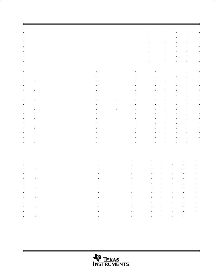
The TL7757 is a supply-voltage supervisor designed for use in microcomputer and microprocessor systems. The supervisor monitors the supply voltage for undervoltage conditions. During power up, when the supply voltage, VCC, attains a value approaching 1 V, the
RESET output becomes active (low) to prevent undefined operation. If the supply voltage drops
below threshold voltage level (VIT±), the RESET output goes to the active (low) level until the supply undervoltage fault condition is eliminated.
The TL7757C is characterized for operation from 0°C to 70°C. The TL7757I is characterized for operation from ±40°C to 85°C.
PK PACKAGE (TOP VIEW)
VCC GND RESET
GND is in electrical contact with the tab.
AVAILABLE OPTIONS
|
PACKAGED DEVICES |
|
CHIP FORM |
||
TA |
|
|
|
||
SMALL OUTLINE |
TO-226AA |
SOT-89 |
|||
(Y) |
|||||
|
(D) |
(LP) |
(PK) |
|
|
0°C to 70°C |
TL7757CD |
TL7757CLP |
TL7757CPK |
TL7757Y |
|
|
|
|
|
||
±40°C to 85°C |
TL7757ID |
TL7757ILP |
TL7757IPK |
||
|
|||||
D and LP packages are available taped and reeled. Add the suffix R to device type (e.g.,
TL7757CDR). Chip forms are tested at 25°C.
Please be aware that an important notice concerning availability, standard warranty, and use in critical applications of Texas Instruments semiconductor products and disclaimers thereto appears at the end of this data sheet.
PRODUCTION DATA information is current as of publication date. Products conform to specifications per the terms of Texas Instruments standard warranty. Production processing does not necessarily include testing of all parameters.
Copyright 1999, Texas Instruments Incorporated
POST OFFICE BOX 655303 •DALLAS, TEXAS 75265 |
1 |

TL7757
SUPPLY-VOLTAGE SUPERVISOR
AND PRECISION VOLTAGE DETECTOR
SLVS041E ± SEPTEMBER 1991 ± REVISED JULY 1999
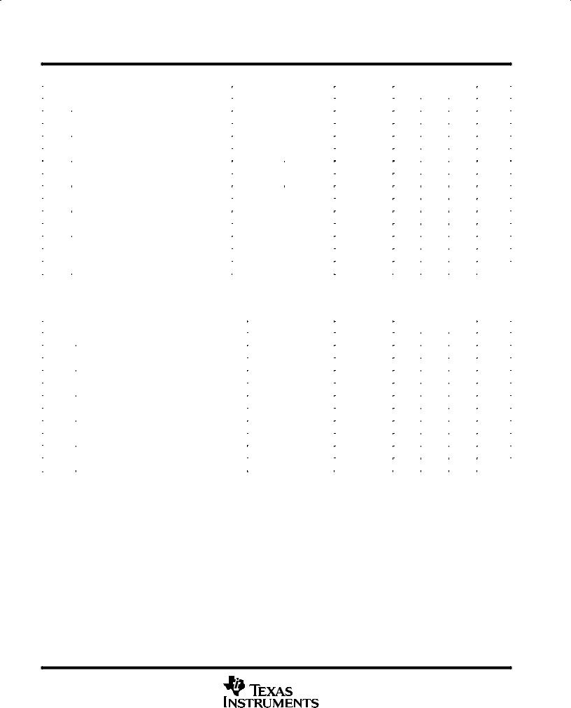
equivalent schematic
|
|
|
VCC |
|
|
|
|
RESET |
|
R2 |
|
|
|
Q8 |
Q11 |
R15 |
|
|
|
Q2 |
|
|
|
|
||
|
|
|
|
|
|
|
||
|
|
|
Q5 |
R12 |
|
|
Q15 |
Q19 |
|
R3 |
|
|
|
|
|
||
|
|
R5 |
|
|
|
|
Q13 |
|
|
|
|
|
|
|
Q17 |
Q21 |
|
|
|
|
R11 |
|
|
|
||
R1 |
|
|
|
|
|
C2 |
R16 |
|
R4 |
|
|
Q7 |
Q9 |
|
|
Q20 |
|
|
R6 |
R10 |
|
|
||||
|
|
|
|
|
R14 |
|
||
|
|
|
|
|
|
|
|
|
|
|
|
Q6 |
|
|
|
Q18 |
|
|
|
|
R8 |
|
|
|
|
|
|
|
Q3 |
Q4 |
C1 |
Q10 |
Q12 |
Q14 |
|
|
|
|
R9 |
Q16 |
R18 |
|||
|
|
|
|
|
|
|
||
|
Q1 |
|
|
|
|
|
|
|
|
|
|
|
|
|
|
|
|
|
|
R7 |
|
|
R13 |
|
|
|
GND
ACTUAL DEVICE
COMPONENT COUNT
Transistors 27
Resistors 20
Capacitors 2
absolute maximum ratings over operating free-air temperature (unless otherwise noted)²
Supply voltage range, VCC (see Note 1) . . . . . . . . . . . . . . . . . . . . . . . . . . . . . . . . . . . . . . . . . . . . . |
±0.3 V to 20 V |
Offstate output voltage range (see Note 1) . . . . . . . . . . . . . . . . . . . . . . . . . . . . . . . . . . . . . . . . . . . |
±0.3 V to 20 V |
Output current, IO . . . . . . . . . . . . . . . . . . . . . . . . . . . . . . . . . . . . . . . . . . . . . . . . . . . . . . . . . . . . . . . . . |
. . . . . . . 30 mA |
Package thermal impedance, θJA (see Notes 2 and 3): D package . . . . . . . . . . . . . . . . . . . . . . |
. . . . . . 97°C/W |
LP package . . . . . . . . . . . . . . . . . . . . . |
. . . . . 156°C/W |
PK package . . . . . . . . . . . . . . . . . . . . . |
. . . . . . 52°C/W |
Lead temperature 1,6 mm (1/16 inch) from case for 10 seconds . . . . . . . . . . . . . . . . . . . . . . . . |
. . . . . . . 260°C |
Storage temperature range, Tstg . . . . . . . . . . . . . . . . . . . . . . . . . . . . . . . . . . . . . . . . . . . . . . . . . . . |
±65°C to 150°C |
²Stresses beyond those listed under ªabsolute maximum ratingsº may cause permanent damage to the device. These are stress ratings only, and functional operation of the device at these or any other conditions beyond those indicated under ªrecommended operating conditionsº is not implied. Exposure to absolute-maximum-rated conditions for extended periods may affect device reliability.
NOTES: 1. All voltage values are with respect to network terminal ground.
2.Maximum power dissipation is a function of TJ(max), θJA, and TA. The maximum allowable power dissipation at any allowable ambient temperature is PD = (TJ(max) ± TA)/θJA. Operating at the absolute maximum TJ of 150°C can impact reliability.
3.The package thermal impedance is calculated in accordance with JESD 51, except for through-hole packages, which use a trace length of zero.
2 |
POST OFFICE BOX 655303 •DALLAS, TEXAS 75265 |
TL7757
SUPPLY-VOLTAGE SUPERVISOR
AND PRECISION VOLTAGE DETECTOR
SLVS041E ± SEPTEMBER 1991 ± REVISED JULY 1999
recommended operating conditions
|
|
MIN |
MAX |
UNIT |
|
|
|
|
|
|
|
Supply voltage, VCC |
|
1 |
7 |
V |
|
High-level output voltage, VOH |
|
|
15 |
V |
|
Low-level output current, IOL |
|
|
20 |
mA |
|
Operating free-air temperature, TA |
TL7757C |
0 |
70 |
°C |
|
|
|
|
|||
TL7757I |
±40 |
85 |
|||
|
|
||||
|
|
|
|
|
electrical characteristics at specified free-air temperature
|
PARAMETER |
TEST CONDITIONS |
TA |
|
TL7757C |
|
UNIT |
|||
|
|
|
|
|
||||||
|
MIN |
TYP |
MAX |
|||||||
|
|
|
|
|
|
|
||||
|
|
|
|
|
|
|
|
|
|
|
VIT ± |
Negative-going input threshold voltage at VCC |
|
|
|
25°C |
4.43 |
4.55 |
4.67 |
V |
|
|
|
|
|
|
|
|
|
|||
|
|
|
0°C to 70°C |
4.4 |
|
|
4.7 |
|||
|
|
|
|
|
|
|
|
|||
|
|
|
|
|
|
|
|
|
|
|
Vhys² |
Hysteresis at VCC |
|
|
|
25°C |
40 |
50 |
60 |
mV |
|
|
|
|
|
|
|
|
|
|||
|
|
|
0°C to 70°C |
30 |
|
|
70 |
|||
|
|
|
|
|
|
|
|
|||
VOL |
Low-level output voltage |
IOL = 20 mA, |
VCC = 4.3 V |
25°C |
|
0.4 |
0.8 |
V |
||
0°C to 70°C |
|
|
|
0.8 |
||||||
|
|
|
|
|
|
|
|
|
||
IOH |
High-level output current |
VCC = 7 V, |
|
VOH = 15 V, |
25°C |
|
|
|
1 |
µA |
See Figure 1 |
|
0°C to 70°C |
|
|
|
1 |
||||
|
|
|
|
|
|
|
||||
³ |
Power-up reset voltage |
RL = 2.2 kΩ, |
|
25°C |
|
0.8 |
1 |
V |
||
Vres |
VCC slew rate ≤ 5 V/µs |
0°C to 70°C |
|
|
|
1.2 |
||||
|
|
|
|
|
|
|||||
|
|
VCC = 4.3 V |
|
25°C |
|
1400 |
2000 |
|
||
|
|
|
|
|
|
|
|
µA |
||
ICC |
Supply current |
|
0°C to 70°C |
|
|
|
2000 |
|||
|
|
|
|
|
|
|||||
|
|
VCC = 5.5 V |
|
0°C to 70°C |
|
|
|
40 |
|
|
² This is the difference between positive-going input threshold voltage, V |
IT+ |
, and negative-going input threshold voltage, V |
. |
|
||||||
|
|
|
|
|
|
|
IT ± |
|
|
|
³ This is the lowest voltage at which RESET becomes active.
switching characteristics at specified free-air temperature
|
PARAMETER |
TEST CONDITIONS |
TA |
|
TL7757C |
|
UNIT |
||
|
|
|
|
||||||
|
MIN |
TYP |
MAX |
||||||
|
|
|
|
|
|
|
|||
|
|
|
|
|
|
|
|
|
|
tPLH |
Propagation delay time, low-to-high-level |
VCC slew rate ≤ 5 V/ |
|
s, |
25°C |
|
3.4 |
5 |
µs |
|
|
|
|
|
|||||
output |
See Figures 2 and 3 |
|
|
0°C to 70°C |
|
|
5 |
||
|
|
|
|
|
|
||||
|
|
|
|
|
|
|
|
|
|
tPHL |
Propagation delay time, high-to-low-level |
See Figures 2 and 3 |
|
|
25°C |
|
2 |
5 |
µs |
output |
|
|
0°C to 70°C |
|
|
5 |
|||
|
|
|
|
|
|
|
|||
|
|
|
|
|
|
|
|
|
|
tr |
Rise time |
VCC slew rate ≤ 5 V/ |
|
s, |
25°C |
|
0.4 |
1 |
µs |
|
|
|
|
|
|||||
See Figures 2 and 3 |
|
|
0°C to 70°C |
|
|
1 |
|||
|
|
|
|
|
|
|
|||
|
|
|
|
|
|
|
|
|
|
tf |
Fall time |
See Figures 2 and 3 |
|
|
25°C |
|
0.05 |
1 |
µs |
|
|
|
|
|
|
||||
|
|
0°C to 70°C |
|
|
1 |
||||
|
|
|
|
|
|
|
|
||
tw(min) |
Minimum pulse duration at VCC for output |
|
|
|
25°C |
|
|
5 |
µs |
response |
|
|
|
0°C to 70°C |
|
|
5 |
||
|
|
|
|
|
|
|
|||
|
|
|
|
|
|
|
|
|
|
POST OFFICE BOX 655303 •DALLAS, TEXAS 75265 |
3 |
TL7757
SUPPLY-VOLTAGE SUPERVISOR
AND PRECISION VOLTAGE DETECTOR
SLVS041E ± SEPTEMBER 1991 ± REVISED JULY 1999
electrical characteristics at specified free-air temperature
|
PARAMETER |
TEST CONDITIONS |
TA |
|
TL7757I |
|
UNIT |
||
|
|
|
|
|
|||||
|
MIN |
TYP |
MAX |
||||||
|
|
|
|
|
|
||||
|
|
|
|
|
|
|
|
|
|
VIT ± |
Negative-going input threshold voltage at VCC |
|
|
25°C |
4.43 |
4.55 |
4.67 |
V |
|
|
|
|
|
|
|
|
|||
|
|
±40°C to 85°C |
4.4 |
|
|
4.7 |
|||
|
|
|
|
|
|
|
|||
Vhys² |
Hysteresis at VCC |
|
|
25°C |
40 |
50 |
60 |
mV |
|
|
|
±40°C to 85°C |
30 |
|
|
70 |
|||
|
|
|
|
|
|
|
|||
VOL |
Low-level output voltage |
IOL = 20 mA, |
VCC = 4.3 V |
25°C |
|
0.4 |
0.8 |
V |
|
±40°C to 85°C |
|
|
|
0.8 |
|||||
|
|
|
|
|
|
|
|
||
IOH |
High-level output current |
VCC = 7 V, |
VOH = 15 V, |
25°C |
|
|
|
1 |
µA |
See Figure 1 |
|
±40°C to 85°C |
|
|
|
1 |
|||
|
|
|
|
|
|
|
|||
|
|
|
|
|
|
|
|
|
|
³ |
Power-up reset voltage |
RL = 2.2 kΩ, |
|
25°C |
|
0.8 |
1 |
V |
|
Vres |
VCC slew rate ≤ 5 V/µs |
±40°C to 85°C |
|
|
|
1.2 |
|||
|
|
|
|
|
|
||||
|
|
VCC = 4.3 V |
|
25°C |
|
1400 |
2000 |
|
|
|
|
|
|
|
|
|
|
µA |
|
ICC |
Supply current |
|
±40°C to 85°C |
|
|
|
2100 |
||
|
|
|
|
|
|||||
|
|
VCC = 5.5 V |
|
±40°C to 85°C |
|
|
|
40 |
|
² This is the difference between positive-going input threshold voltage, V |
, and negative-going input threshold voltage, V |
. |
|
||||||
|
|
|
IT+ |
|
|
|
IT ± |
|
|
³ This is the lowest voltage at which RESET becomes active.
switching characteristics at specified free-air temperature
|
PARAMETER |
TEST CONDITIONS |
TA |
|
TL7757I |
|
UNIT |
|
|
|
|
||||
|
MIN |
TYP |
MAX |
||||
|
|
|
|
|
|||
|
|
|
|
|
|
|
|
tPLH |
Propagation delay time, low-to-high-level output |
VCC slew rate ≤ 5 V/µs, |
25°C |
|
3.4 |
5 |
µs |
See Figures 2 and 3 |
±40°C to 85°C |
|
|
5 |
|||
|
|
|
|
|
|||
|
|
|
|
|
|
|
|
tPHL |
Propagation delay time, high-to-low-level output |
See Figures 2 and 3 |
25°C |
|
2 |
5 |
µs |
|
|
|
|
||||
±40°C to 85°C |
|
|
5 |
||||
|
|
|
|
|
|
||
|
|
|
|
|
|
|
|
|
|
|
25°C |
|
0.4 |
1 |
|
tr |
Rise time |
VCC slew rate ≤ 5 V/ s, |
|
|
|
|
µs |
See Figures 2 and 3 |
±40°C to 85°C |
|
|
1 |
|||
|
|
|
|
|
|||
tf |
Fall time |
See Figures 2 and 3 |
25°C |
|
0.05 |
1 |
µs |
±40°C to 85°C |
|
|
1 |
||||
|
|
|
|
|
|
||
tw(min) |
Minimum pulse duration at VCC for output |
|
25°C |
|
|
5 |
µs |
response |
|
±40°C to 85°C |
|
|
5 |
||
|
|
|
|
|
|||
|
|
|
|
|
|
|
|
4 |
POST OFFICE BOX 655303 •DALLAS, TEXAS 75265 |
 Loading...