


TL1431CKTPR
Texas Instruments TL1431CKTPR, TL1431CDR, TL1431CD, TL1431MFKB, TL1431MFK Datasheet
...
TL1431
PRECISION PROGRAMMABLE REFERENCE
SLVS062F – DECEMBER 1991 – REVISED JANUAR Y 2000
D
0.4% Initial Voltage Tolerance
D
0.2-Ω Typical Output Impedance
D
Fast Turnon . . . 500 ns
D
Sink Current Capability ...1 mA to 100 mA
D
Low Reference Current (REF)
D
Adjustable Output Voltage ...V
I(ref)
description
The TL1431 is a precision programmable
reference with specified thermal stability over
automotive, commercial, and military
temperature ranges. The output voltage can be
set to any value between V
2.5 V) and 36 V with two external resistors (see
Figure 16). This device has a typical output
impedance of 0.2 Ω. Active output circuitry
provides a very sharp turnon characteristic,
making the device an excellent replacement for
zener diodes and other types of references in
applications such as onboard regulation,
adjustable power supplies, and switching power
supplies.
The TL1431C is characterized for operation over
the commercial temperature range of 0°C to
70°C. The TL1431Q is characterized for
operation over the full automotive temperature
range of –40°C to 125°C. The TL1431M is
characterized for operation over the full military
temperature range of –55°C to 125°C.
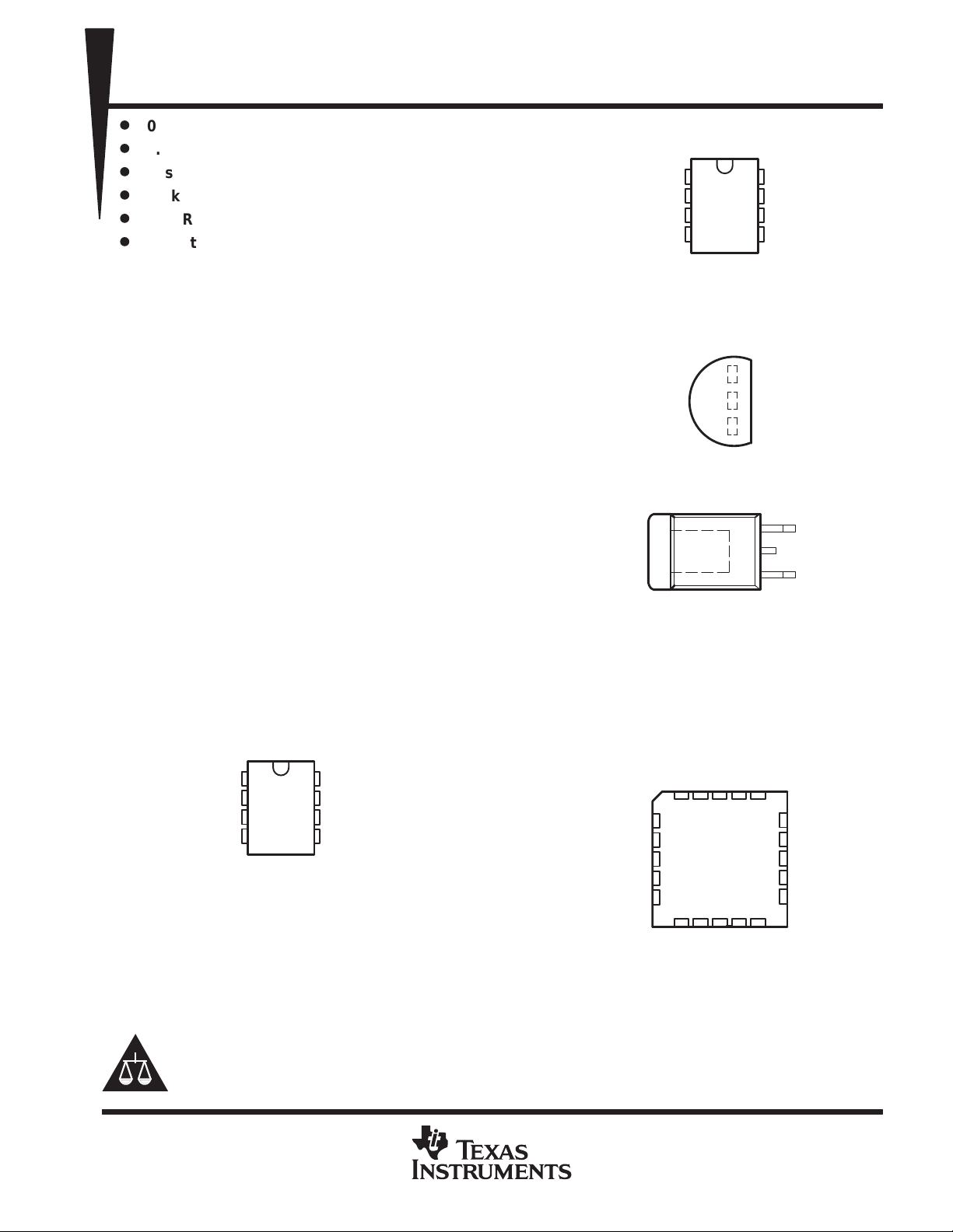
JG PACKAGE
(TOP VIEW)
(approximately
I(ref)
to 36 V
D PACKAGE
(TOP VIEW)
CATHODE
ANODE
ANODE
NC – No internal connection
ANODE terminals are connected internally.
1
2
3
NC
4
LP PACKAGE
(TOP VIEW)
8
7
6
5
REF
ANODE
ANODE
NC
CATHODE
ANODE
REF
KTP PACKAGE
(TOP VIEW)
CATHODE
ANODE
ANODE
REF
The ANODE terminal is in electrical contact with the
mounting base.
FK PACKAGE
(TOP VIEW)
CATHODE
NC – No internal connection
Please be aware that an important notice concerning availability, standard warranty, and use in critical applications of
Texas Instruments semiconductor products and disclaimers thereto appears at the end of this data sheet.
PRODUCTION DATA information is current as of publication date.
Products conform to specifications per the terms of Texas Instruments
standard warranty. Production processing does not necessarily include
testing of all parameters.
NC
NC
NC
1
2
3
4
8
7
6
5
REF
NC
ANODE
NC
POST OFFICE BOX 655303 • DALLAS, TEXAS 75265
NC
CATHODE
NC
REF
NC
NC
NC
NC
NC
NC
3212019
4
5
6
7
8
910111213
NCNCNC
Copyright 2000, Texas Instruments Incorporated
On products compliant to MIL-PRF-38535, all parameters are tested
unless otherwise noted. On all other products, production
processing does not necessarily include testing of all parameters.
NC
18
17
16
15
14
NC
NC
NC
NC
ANODE
NC
1

TL1431
PRECISION PROGRAMMABLE REFERENCE
SLVS062F – DECEMBER 1991 – REVISED JANUAR Y 2000
AVAILABLE OPTIONS
PACKAGED DEVICES
PLASTIC
FLANGE
MOUNTED
(KTP)
0°C to 70°C TL1431CD TL1431CKTPR TL1431CLP – –
–40°C to 125°C TL1431QD – TL1431QLP – –
–55°C to 125°C – – – TL1431MFK TL1431MJG
The D and LP packages are available taped and reeled. The KTP package is only available taped and reeled. Add the suffix R
to the device type (e.g., TL1431CDR). Chip forms are tested at 25°C.
logic symbol
T
A
SMALL
OUTLINE
(D)
TO-226AA
(LP)
REF
CHIP
CARRIER
(FK)
CERAMIC
DIP
(JG)
CHIP
FORM
(Y)
TL1431Y
functional block diagram
REF
ANODE
V
ref
CATHODE
CATHODE
+
–
ANODE
2
POST OFFICE BOX 655303 • DALLAS, TEXAS 75265

TL1431
PRECISION PROGRAMMABLE REFERENCE
SLVS062F – DECEMBER 1991 – REVISED JANUAR Y 2000
equivalent schematic
REF
1
8
2.4 kΩ
2,3,6,7
CATHODE
ANODE
†
3.28 kΩ
7.2 kΩ
20 pF
800 Ω
800 Ω
800 Ω
20 pF
150 Ω
4 kΩ
10 kΩ
1 kΩ
†
All component values are nominal.
Pin numbers shown are for the D package.
POST OFFICE BOX 655303 • DALLAS, TEXAS 75265
3
TL1431
PRECISION PROGRAMMABLE REFERENCE
SLVS062F – DECEMBER 1991 – REVISED JANUAR Y 2000
absolute maximum ratings over operating free-air temperature range (unless otherwise noted)
Cathode voltage,VKA (see Note 1) 37 V. . . . . . . . . . . . . . . . . . . . . . . . . . . . . . . . . . . . . . . . . . . . . . . . . . . . . . . . . . .
Continuous cathode current range, IKA –100 mA to 150 mA. . . . . . . . . . . . . . . . . . . . . . . . . . . . . . . . . . . . . . . . .
Reference input current range, I
Package thermal impedance, θJA (see Notes 2 and 3): D package 97°C/W. . . . . . . . . . . . . . . . . . . . . . . . . . . .
Lead temperature 1,6 mm (1/16 inch) from case for 10 seconds 260°C. . . . . . . . . . . . . . . . . . . . . . . . . . . . . . .
Storage temperature range, T
†
Stresses beyond those listed under “absolute maximum ratings” may cause permanent damage to the device. These are stress ratings only, and
functional operation of the device at these or any other conditions beyond those indicated under “recommended operating conditions” is not implied.
Exposure to absolute-maximum-rated conditions for extended periods may affect device reliability.
NOTES: 1. All voltage values are with respect to ANODE unless otherwise noted.
2. Maximum power dissipation is a function of TJ(max),
temperature is PD = (TJ(max) – TA)/
3. The package thermal impedance is calculated in accordance with JESD 51.
PACKAGE
FK 1375 mW 11.0 mW/°C 880 mW 715 mW 275 mW
JG 1050 mW 8.4 mW/°C 672 mW 546 mW 210 mW
TA = 25°C
POWER RATING
stg
POWER DISSIPATION RATING TABLE – FREE-AIR TEMPERATURE
–50 µA to 10 mA. . . . . . . . . . . . . . . . . . . . . . . . . . . . . . . . . . . . . . . . . . . . . . .
I(ref)
KTP package 28°C/W. . . . . . . . . . . . . . . . . . . . . . . . .
LP package 156°C/W. . . . . . . . . . . . . . . . . . . . . . . . . .
–65°C to 150°C. . . . . . . . . . . . . . . . . . . . . . . . . . . . . . . . . . . . . . . . . . . . . . . . . . .
θ
, and TA. The maximum allowable power dissipation at any allowable ambient
θ
. Operating at the absolute maximum TJ of 150°C can impact reliability.
JA
DERATING
FACTOR ABOVE
TA = 25°C
JA
TA = 70°C
POWER RATING
TA = 85°C
POWER RATING
TA = 125°C
POWER RATING
†
recommended operating conditions
V
I
T
KA
KA
A
Cathode voltage V
Cathode current 1 100 mA
Operating free-air temperature
MIN MAX UNIT
I(ref)
TL1431C 0 70
TL1431Q
TL1431M –55 125
–40 125
36 V
°C
4
POST OFFICE BOX 655303 • DALLAS, TEXAS 75265

PARAMETER
TEST CONDITIONS
T
†
UNIT
Reference
Reference
Off-state
TL1431
PRECISION PROGRAMMABLE REFERENCE
SLVS062F – DECEMBER 1991 – REVISED JANUAR Y 2000
electrical characteristics at specified free-air temperature, IKA = 10 mA (unless otherwise noted)
A
25°C 2490 2500 2510
V
I(ref)
V
I(dev)
D
D
I
I(ref)
I
I(dev)
I
off
|zKA|
†
Full range is 0°C to 70°C for C-suffix devices.
‡
The deviation parameters V
temperature range. The average full-range temperature coefficient of the reference input voltage
input voltage
Deviation of reference input
voltage over full temperature
‡
range
Ratio of change in reference
V
)
I(ref
input voltage to the change in
V
KA
cathode voltage
input current
Deviation of reference input
current over full temperature
‡
range
Minimum cathode current for
regulation
cathode current
Output impedance
ppm
ǒ
Ť
a
V
I(ref
where:
∆TA is the rated operating temperature range of the device.
Ǔ
Ť
+
°C
)
§
and I
I(dev)
V
)
I(dev
ǒ
V
I(ref
)
at 25
Ǔ
C
°
D
T
A
VKA = V
VKA = V
∆VKA = 3 V to 36 V
R1 = 10 kΩ,
R1 = 10 kΩ, R2 = ∞
VKA = V
VKA = 36 V,
VKA = V
IKA = 1 mA to 100 mA
are defined as the differences between the maximum and minimum values obtained over the rated
I(dev)
6
10
I(ref)
I(ref)
R2 = ∞
to 36 V 25°C Figure 1 0.45 1 mA
I(ref)
V
I(ref)
, f ≤ 1 kHz,
I(ref)
Max V
I(ref)
Full
range
Full
range
Full
range
25°C 1.5 2.5
Full
range
Full
range
25°C 0.18 0.5
= 0
Full
range
25°C Figure 1 0.2 0.4 Ω
TEST
CIRCUIT
Figure 1
Figure 1 4 20 mV
Figure 2 –1.1 –2 mV/V
Figure 2
Figure 2 0.2 1.2 µA
Figure 3
is defined as:
a
V
)
I(ref
TL1431C
MIN TYP MAX
2480 2520
mV
µA
3
µA
2
V
I(dev)
a
is positive or negative depending on whether minimum V
V
)
I(ref
§
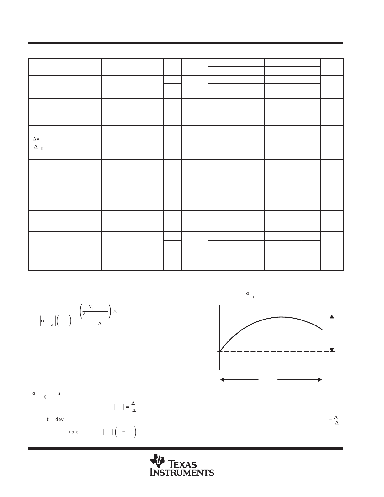
The output impedance is defined as:
When the device is operating with two external resistors (see Figure 2), the total dynamic impedance of the circuit is given by: |z′|+
which is approximately equal to
Min V
I(ref)
∆T
A
or maximum V
I(ref)
D
V
Ť
z
KA
Ť
Ť
ǒ
z
1
KA
KA
Ť
+
D
I
KA
R1
Ǔ
)
.
R2
POST OFFICE BOX 655303 • DALLAS, TEXAS 75265
, respectively, occurs at the lower temperature.
I(ref)
D
V
,
D
I
5
TL1431
PARAMETER
TEST CONDITIONS
T
†
UNIT
Reference
Reference
Off-state
PRECISION PROGRAMMABLE REFERENCE
SLVS062F – DECEMBER 1991 – REVISED JANUAR Y 2000
electrical characteristics at specified free-air temperature, IKA = 10 mA (unless otherwise noted)
TEST
A
CIRCUIT
25°C 2490 2500 2510 2475 2500 2540
V
I(ref)
V
I(dev)
D
D
I
I(ref)
I
I(dev)
I
off
|zKA|
*On products compliant to MIL-PRF-38535, this parameter is not production tested.
†
Full range is –40°C to 125°C for Q-suffix devices, and –55°C to 125°C for M-suffix devices.
‡
The deviation parameters V
temperature range. The average full-range temperature coefficient of the reference input voltage
input voltage
Deviation of
reference input
voltage over full
temperature range
Ratio of change in
reference input
V
)
I(ref
voltage to the
V
KA
change in cathode
voltage
input current
Deviation of
reference input
current over full
temperature range
Minimum
cathode current
for regulation
cathode current
Output impedance
ǒ
ppm
ǒ
Ť
Ť
a
V
°C
)
I(ref
where:
∆TA is the rated operating temperature range of the device.
V
Ǔ
+
VKA = V
VKA = V
‡
∆VKA = 3 V to 36 V
R1 = 10 kΩ,
R1 = 10 kΩ, R2 = ∞
‡
VKA = V
VKA = 36 V,
VKA = V
§
IKA = 1 mA to 100 mA
and I
I(dev)
V
)
I(dev
Ǔ
C
at 25
°
)
I(ref
D
T
A
Figure 1
I(ref)
I(ref)
R2 = ∞
to 36 V 25°C Figure 1 0.45 1 0.45 1 mA
I(ref)
V
I(ref)
, f ≤ 1 kHz,
I(ref)
are defined as the differences between the maximum and minimum values obtained over the rated
I(dev)
6
10
Full
range
Full
range
range
range
range
= 0
range
Figure 1 17 55 17 55* mV
Full
Figure 2 –1.1 –2 –1.1 –2 mV/V
25°C 1.5 2.5 1.5 2.5
Figure 2
Full
Full
Figure 2 0.5 2 0.5 3* µA
25°C 0.18 0.5 0.18 0.5
Figure 3
Full
25°C Figure 1 0.2 0.4 0.2 0.4 Ω
Max V
I(ref)
TL1431Q TL1431M
MIN TYP MAX MIN TYP MAX
2470 2530 2460 2550
4 5
2 2
a
is defined as:
V
)
I(ref
mV
µA
µA
V
I(dev)
a
V
§
The output impedance is defined as:
When the device is operating with two external resistors (see Figure 2), the total dynamic impedance of the circuit is given by: |z′|+
which is approximately equal to
6
is positive or negative depending on whether minimum V
)
I(ref
D
V
Ť
z
KA
Ť
Ť
ǒ
z
1
KA
KA
Ť
+
D
I
KA
R1
Ǔ
)
.
R2
POST OFFICE BOX 655303 • DALLAS, TEXAS 75265
Min V
or maximum V
I(ref)
I(ref)
∆T
A
, respectively, occurs at the lower temperature.
I(ref)
D
V
,
D
I
 Loading...