


Texas Instruments TL1451AQDR, TL1451AQD, TL1451AMJB, TL1451AMJ, TL1451AMFKB Datasheet
...TL1451A DUAL PULSE-WIDTH-MODULATION CONTROL CIRCUITS
DComplete PWM Power Control Circuitry
DCompletely Synchronized Operation
DInternal Undervoltage Lockout Protection
DWide Supply Voltage Range
DInternal Short-Circuit Protection
DOscillator Frequency . . . 500 kHz Max
DVariable Dead Time Provides Control Over Total Range
DInternal Regulator Provides a Stable 2.5-V Reference Supply
DAvailable in Q-Temp Automotive
HighRel Automotive Applications Configuration Control / Print Support Qualification to Automotive Standards
SLVS024E ± FEBRUARY 1983 ± REVISED NOVEMBER 1999
D, DB, N, NS, PW, OR J PACKAGE
(TOP VIEW)
|
|
CT |
|
1 |
|
16 |
|
REF |
|
||
|
|
|
|
|
|
||||||
|
|
RT |
|
2 |
|
15 |
|
SCP |
|
||
|
|
|
|
|
|||||||
ERROR |
|
1IN+ |
|
3 |
|
14 |
|
2IN+ |
|
|
ERROR |
|
|
|
|
|
|||||||
|
|
|
|
|
|||||||
AMPLIFIER 1 |
|
1IN± |
|
4 |
|
13 |
|
2IN± |
|
|
AMPLIFIER 2 |
|
|
|
|
|
|||||||
1FEEDBACK |
|
5 |
|
12 |
|
2FEEDBACK |
|||||
|
|
|
|||||||||
|
1DTC |
|
6 |
|
11 |
|
2DTC |
|
|||
|
|
|
|
|
|||||||
|
1OUT |
|
7 |
|
10 |
|
2OUT |
|
|||
|
|
|
|
|
|||||||
|
|
GND |
|
8 |
|
9 |
|
VCC |
|
||
|
|
|
|
|
|||||||
|
|
|
|
|
|
|
|
|
|
|
|
|
|
|
FK PACKAGE |
|
|||||||
|
|
|
|
(TOP VIEW) |
|
|
|
|
|||
|
|
RT |
|
CT |
NC |
REF |
SCP |
|
|||
description
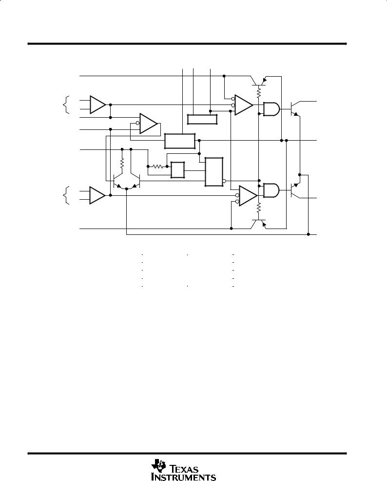
The TL1451A incorporates on a single monolithic chip all the functions required in the construction of two pulse-width-modulation (PWM) control circuits. Designed primarily for power-supply control, the TL1451A contains an on-chip 2.5-V regulator, two error amplifiers, an adjustable oscillator, two dead-time comparators, undervoltage lockout circuitry, and dual common-emitter output transistor circuits.
|
3 |
2 |
1 |
20 |
19 |
|
1IN+ |
4 |
|
|
|
18 |
2IN+ |
1IN± |
5 |
|
|
|
17 |
2IN± |
NC |
6 |
|
|
|
16 |
NC |
1FEEDBACK |
7 |
|
|
|
15 |
2FEEDBACK |
IDTC |
8 |
|
|
|
14 |
2DTC |
|
9 |
10 |
11 |
12 |
13 |
|
|
1OUT |
GND |
NC |
CC |
2OUT |
|
|
V |
|
The uncommitted output transistors provide common-emitter output capability for each
controller. The internal amplifiers exhibit a common-mode voltage range from 1.04 V to 1.45 V. The dead-time control (DTC) comparator has no offset unless externally altered and can provide 0% to 100% dead time. The on-chip oscillator can be operated by terminating RT and CT. During low VCC conditions, the undervoltage lockout control circuit feature locks the outputs off until the internal circuitry is operational.
The TL1451AC is characterized for operation from ±20°C to 85°C. The TL1451AQ is characterized for operation from ±40°C to 125°C. The TL1451AM is characterized for operation from ±55°C to 125°C.
AVAILABLE OPTIONS
|
|
|
PACKAGED DEVICES |
|
|
|||
|
|
|
|
|
|
|
|
|
TA |
SMALL |
SMALL |
PLASTIC DIP |
SMALL |
TSSOP |
CHIP |
CERAMIC |
|
OUTLINE |
OUTLINE |
OUTLINE |
CARRIER |
DIP |
||||
|
(N) |
(PW)² |
||||||
|
(D) |
(DB)² |
(NS) |
(FK) |
(J) |
|||
|
|
|
||||||
± 20°C to 85°C |
Ð |
TL1451ACDB |
TL1451ACN |
TL1451ACNS |
TL1451ACPW |
Ð |
Ð |
|
|
|
|
|
|
|
|
|
|
± 40°C to 125°C |
TL1451AQD |
Ð |
Ð |
Ð |
Ð |
Ð |
Ð |
|
|
|
|
|
|
|
|
|
|
± 55°C to 125°C |
Ð |
Ð |
Ð |
Ð |
Ð |
TL1451AMFK |
TL1451AMJ |
|
|
|
|
|
|
|
|
|
|
² The DB and PW packages are only available left-end taped and reeled (add LE suffix, i.e., TL1451ACPWLE).
Please be aware that an important notice concerning availability, standard warranty, and use in critical applications of Texas Instruments semiconductor products and disclaimers thereto appears at the end of this data sheet.
PRODUCTION DATA information is current as of publication date. Products conform to specifications per the terms of Texas Instruments standard warranty. Production processing does not necessarily include testing of all parameters.
Copyright 1999, Texas Instruments Incorporated
On products compliant to MIL-PRF-38535, all parameters are tested unless otherwise noted. On all other products, production processing does not necessarily include testing of all parameters.
POST OFFICE BOX 655303 •DALLAS, TEXAS 75265 |
1 |
TL1451A
DUAL PULSE-WIDTH-MODULATION CONTROL CIRCUITS
SLVS024E ± FEBRUARY 1983 ± REVISED NOVEMBER 1999
functional block diagram
|
|
|
|
VCC RT |
CT |
|
|
|
2 DTC |
11 |
|
9 |
2 |
1 |
|
|
|
|
|
|
|
|
|
|
||
ERROR |
IN + |
14 |
+ |
|
|
|
10 2 OUTPUT |
|
AMPLIFIER 2 |
IN ± |
13 |
± |
|
|
|
|
|
|
12 |
|
|
|
|
|
||
2 FEEDBACK |
1/2 Vref |
|
Oscillator |
PWM |
|
|||
|
|
5 |
|
|
|
COMP |
|
|
1 FEEDBACK |
|
|
|
|
|
|
||
|
|
|
12 kΩ |
Reference |
|
16 |
REF |
|
|
SCP |
15 |
Voltage |
|
|
|
|
|
|
|
|
|
|
|
|
||
|
|
|
170 kΩ |
R |
|
UVLO |
|
|
|
|
|
|
|
R |
|
|
|
|
|
|
|
S |
|
|
|
|
|
|
|
|
|
|
|
|
|
ERROR |
IN + |
3 |
+ |
|
|
|
7 1 OUTPUT |
|
AMPLIFIER 1 |
IN ± |
4 |
± |
|
|
|
||
|
|
|
|
|
|
|
PWM |
|
|
|
|
|
|
|
|
COMP |
|
1 DTC |
6 |
|
|
|
|
8 |
|
|
|
|
|
|
|
GND |
|||
|
|
|
|
|
|
|
||
|
|
|
|
|
|
|
|
|
COMPONENT COUNT
Resistors |
65 |
Capacitors |
8 |
Transistors |
105 |
JFETs |
18 |
2 |
POST OFFICE BOX 655303 •DALLAS, TEXAS 75265 |

|
TL1451A |
|
DUAL PULSE-WIDTH-MODULATION CONTROL CIRCUITS |
||
|
SLVS024E ± FEBRUARY 1983 ± REVISED NOVEMBER 1999 |
|
|
|
|
absolute maximum ratings over operating free-air temperature range² |
||
Supply voltage, VCC . . . . . . . . . . . . . . . . . . . . . . . . . . . . . . . . . . . . . |
. . . . . . . . . . . . . . . . . . . . . . . . . . . . . . . . . . 51 V |
|
Amplifier input voltage, VI . . . . . . . . . . . . . . . . . . . . . . . . . . . . . . . . . |
. . . . . . . . . . . . . . . . . . . . . . . . . . . . . . . . . . 20 V |
|
Collector output voltage, VO . . . . . . . . . . . . . . . . . . . . . . . . . . . . . . . |
. . . . . . . . . . . . . . . . . . . . . . . . . . . . . . . . . . 51 V |
|
Collector output current, IO . . . . . . . . . . . . . . . . . . . . . . . . . . . . . . . . |
. . . . . . . . . . . . . . . . . . . . . . . . . . . . . . . . 21 mA |
|
Continuous power total dissipation . . . . . . . . . . . . . . . . . . . . . . . . . |
. . . . . . . . . . . . See Dissipation Rating Table |
|
Operating free-air temperature range, TA C suffix . . . . . . . . . . . . |
. . . . . . . . . . . . . . . . . . . . . . . . . ±20°C to 85°C |
|
Q suffix . . . . . . . . . . . . |
. . . . . . . . . . . . . . . . . . . . . . . . ±40°C to 125°C |
|
M suffix . . . . . . . . . . . . |
. . . . . . . . . . . . . . . . . . . . . . . . ±55°C to 125°C |
|
Storage temperature range, Tstg . . . . . . . . . . . . . . . . . . . . . . . . . . . |
. . . . . . . . . . . . . . . . . . . . . . . . ±65°C to 150°C |
|
Lead temperature 1,6 mm (1/16 inch) from case for 10 seconds |
. . . . . . . . . . . . . . . . . . . . . . . . . . . . . . . 260°C |
|
²Stresses beyond those listed under ªabsolute maximum ratingsº may cause permanent damage to the device. These are stress ratings only, and functional operation of the device at these or any other conditions beyond those indicated under ªrecommended operating conditionsº is not implied. Exposure to absolute-maximum-rated conditions for extended periods may affect device reliability.
DISSIPATION RATING TABLE
PACKAGE |
TA ≤ 25°C |
DERATING FACTOR |
TA = 70°C |
TA = 85°C |
TA = 125°C |
|
POWER RATING |
ABOVE TA = 25°C |
POWER RATING |
POWER RATING |
POWER RATING |
||
|
||||||
D |
1088 mW |
8.7 mW/°C |
696 mW |
566 mW |
218 mW |
|
DB |
775 mW |
6.2 mW/°C |
496 mW |
403 mW |
Ð |
|
N |
1000 mW |
8.0 mW/°C |
640 mW |
520 mW |
Ð |
|
NS |
500 mW |
4.0 mW/°C |
320 mW |
260 mW |
Ð |
|
PW |
838 mW |
6.7 mW/°C |
536 mW |
436 mW |
168 mW |
|
FK |
1375 mW |
11.0 mW/°C |
880 mW |
715 mW |
275 mW |
|
J |
1375 mW |
11.0 mW/°C |
880 mW |
715 mW |
275 mW |
recommended operating conditions
|
|
MIN |
MAX |
UNIT |
|
|
|
|
|
Supply voltage, VCC |
|
3.6 |
50 |
V |
Amplifier input voltage, VI |
|
1.05 |
1.45 |
V |
Collector output voltage, VO |
|
|
50 |
V |
Collector output current, IO |
|
|
20 |
mA |
Current into feedback terminal |
|
|
45 |
µA |
Feedback resistor, RF |
|
100 |
|
kΩ |
Timing capacitor, CT |
|
150 |
15000 |
pF |
Timing resistor, RT |
|
5.1 |
100 |
kΩ |
Oscillator frequency |
|
1 |
500 |
kHz |
|
|
|
|
|
|
C suffix |
± 20 |
85 |
|
Operating free-air temperature, TA |
|
|
|
°C |
Q suffix |
± 40 |
125 |
||
|
M suffix |
± 55 |
125 |
|
|
|
|
|
|
POST OFFICE BOX 655303 •DALLAS, TEXAS 75265 |
3 |

TL1451A
DUAL PULSE-WIDTH-MODULATION CONTROL CIRCUITS
SLVS024E ± FEBRUARY 1983 ± REVISED NOVEMBER 1999
electrical characteristics over recommended operating free-air temperature range, VCC = 6 V, f = 200 kHz (unless otherwise noted)
reference section
PARAMETER |
TEST CONDITIONS |
|
TL1451AC |
|
UNIT |
|
|
|
|
||||
MIN |
TYP² |
MAX |
||||
|
|
|
||||
Output voltage (pin 16) |
IO = 1 mA |
2.4 |
2.5 |
2.6 |
V |
|
Output voltage change with temperature |
TA = ±20°C to 25°C |
|
± 0.1% |
±1% |
|
|
TA = 25°C to 85°C |
|
± 0.2% |
±1% |
|
||
|
|
|
||||
Input voltage regulation |
VCC = 3.6 V to 40 V |
|
2 |
12.5 |
mV |
|
Output voltage regulation |
IO = 0.1 mA to 1 mA |
|
1 |
7.5 |
mV |
|
Short-circuit output current |
VO = 0 |
3 |
10 |
30 |
mA |
|
² All typical values are at T = 25°C. |
|
|
|
|
|
|
A |
|
|
|
|
|
|
undervoltage lockout section |
|
|
|
|
|
PARAMETER |
TEST CONDITIONS |
TL1451AC |
|
UNIT |
||
|
|
|
||||
MIN |
TYP² |
MAX |
||||
|
|
|
||||
Upper threshold voltage (VCC) |
|
|
2.72 |
|
V |
|
Lower threshold voltage (VCC) |
IO(ref) = 0.1 mA, TA = 25°C |
|
2.6 |
|
V |
|
Hysteresis (VCC) |
80 |
120 |
|
mV |
||
|
|
|||||
Reset threshold voltage (VCC) |
|
1.5 |
1.9 |
|
V |
|
² All typical values are at T = 25°C. |
|
|
|
|
|
|
A |
|
|
|
|
|
|
short-circuit protection control section |
|
|
|
|
|
|
PARAMETER |
TEST CONDITIONS |
TL1451AC |
|
UNIT |
|||
|
|
|
|||||
MIN |
TYP² |
MAX |
|||||
|
|
|
|
||||
Input threshold voltage (SCP) |
TA = 25°C |
|
0.65 |
0.7 |
0.75 |
V |
|
Standby voltage (SCP) |
No pullup |
|
140 |
185 |
230 |
mV |
|
|
|
|
|
|
|
|
|
Latched input voltage (SCP) |
No pullup |
|
|
60 |
120 |
mV |
|
|
|
|
|
|
|
|
|
Input (source) current |
VI = 0.7 V, |
TA = 25°C |
±10 |
±15 |
±20 |
µA |
|
Comparator threshold voltage (FEEDBACK) |
|
|
|
1.18 |
|
V |
|
|
|
|
|
|
|
|
|
² All typical values are at T = 25°C. |
|
|
|
|
|
|
|
A |
|
|
|
|
|
|
|
oscillator section |
|
|
|
|
|
|
|
PARAMETER |
TEST CONDITIONS |
|
TL1451C |
|
UNIT |
||
|
|
|
|||||
MIN |
TYP² |
MAX |
|||||
|
|
|
|
||||
Frequency |
CT = 330 pF, |
RT = 10 kΩ |
|
200 |
|
kHz |
|
Standard deviation of frequency |
CT = 330 pF, |
RT = 10 kΩ |
|
10% |
|
|
|
Frequency change with voltage |
VCC = 3.6 V to 40 V |
|
|
1% |
|
|
|
Frequency change with temperature |
TA = ±20°C to 25°C |
|
|
± 0.4% |
± 2% |
|
|
TA = 25°C to 85°C |
|
|
± 0.2% |
± 2% |
|
||
|
|
|
|
||||
² All typical values are at TA = 25°C.
4 |
POST OFFICE BOX 655303 •DALLAS, TEXAS 75265 |
TL1451A
DUAL PULSE-WIDTH-MODULATION CONTROL CIRCUITS
SLVS024E ± FEBRUARY 1983 ± REVISED NOVEMBER 1999
dead-time control section
PARAMETER |
TEST CONDITIONS |
TL1451AC |
|
UNIT |
||
|
|
|
||||
MIN |
TYP² |
MAX |
||||
|
|
|
||||
Input bias current (DTC) |
|
|
|
1 |
µA |
|
Latch mode (source) current (DTC) |
TA = 25°C |
± 80 |
±145 |
|
µA |
|
Latched input voltage (DTC) |
IO = 40 µA |
2.3 |
|
|
V |
|
Input threshold voltage at f = 10 kHz (DTC) |
Zero duty cycle |
|
2.05 |
2.25 |
V |
|
|
|
|
|
|||
Maximum duty cycle |
1.2 |
1.45 |
|
|||
|
|
|
||||
|
|
|
|
|
|
|
² All typical values are at T = 25°C. |
|
|
|
|
|
|
A |
|
|
|
|
|
|
error-amplifier section |
|
|
|
|
|
|
PARAMETER |
TEST CONDITIONS |
|
TL1451AC |
|
UNIT |
||
|
|
|
|||||
MIN |
TYP² |
MAX |
|||||
|
|
|
|
||||
Input offset voltage |
VO (FEEDBACK) = 1.25 V |
|
|
± 6 |
mV |
||
Input offset current |
VO (FEEDBACK) = 1.25 V |
|
|
±100 |
nA |
||
Input bias current |
VO (FEEDBACK) = 1.25 V |
|
160 |
500 |
nA |
||
|
|
|
1.05 |
|
|
|
|
Common-mode input voltage range |
VCC = 3.6 V to 40 V |
to |
|
|
V |
||
|
|
|
1.45 |
|
|
|
|
|
|
|
|
|
|
|
|
Open-loop voltage amplification |
RF = 200 kΩ |
|
70 |
80 |
|
dB |
|
Unity-gain bandwidth |
|
|
|
1.5 |
|
MHz |
|
|
|
|
|
|
|
|
|
Common-mode rejection ratio |
|
|
60 |
80 |
|
dB |
|
|
|
|
|
|
|
||
Positive output voltage swing |
|
|
Vref ± 0.1 |
|
V |
||
Negative output voltage swing |
|
|
|
|
1 |
V |
|
|
|
|
|
|
|
|
|
Output (sink) current (FEEDBACK) |
VID = ± 0.1 V, |
VO = 1.25 V |
0.5 |
1.6 |
|
mA |
|
Output (source) current (FEEDBACK) |
VID = 0.1 V, |
VO = 1.25 V |
± 45 |
±70 |
|
µA |
|
² All typical values are at T = 25°C. |
|
|
|
|
|
|
|
A |
|
|
|
|
|
|
|
output section |
|
|
|
|
|
|
|
PARAMETER |
TEST CONDITIONS |
TL1451AC |
|
UNIT |
||
|
|
|
||||
MIN |
TYP² |
MAX |
||||
|
|
|
||||
Collector off-state current |
VO = 50 V |
|
|
10 |
µA |
|
Output saturation voltage |
IO = 10 mA |
|
1.2 |
2 |
V |
|
Short-circuit output current |
VO = 6 V |
|
90 |
|
mA |
|
² All typical values are at T = 25°C. |
|
|
|
|
|
|
A |
|
|
|
|
|
|
pwm comparator section |
|
|
|
|
|
|
PARAMETER |
TEST CONDITIONS |
TL1451AC |
|
UNIT |
||
|
|
|
||||
MIN |
TYP² |
MAX |
||||
|
|
|
||||
Input threshold voltage at f = 10 kHz (FEEDBACK) |
Zero duty cycle |
|
2.05 |
2.25 |
V |
|
|
|
|
|
|||
Maximum duty cycle |
1.2 |
1.45 |
|
|||
|
|
|
||||
|
|
|
|
|
|
|
² All typical values are at T = 25°C. |
|
|
|
|
|
|
A |
|
|
|
|
|
|
total device |
|
|
|
|
|
|
PARAMETER |
TEST CONDITIONS |
TL1451AC |
|
UNIT |
|
|
|
|
|
|
|||
MIN |
TYP² |
MAX |
|
|||
|
|
|
|
|||
Standby supply current |
Off-state |
|
1.3 |
1.8 |
mA |
|
|
|
|
|
|
|
|
Average supply current |
RT = 10 kΩ |
|
1.7 |
2.4 |
mA |
|
² All typical values are at T = 25°C. |
|
|
|
|
|
|
A |
|
|
|
|
|
|
|
|
|
|
|
|
|
|
|
|
|
|
|
|
POST OFFICE BOX 655303 •DALLAS, TEXAS 75265 |
5 |
TL1451A
DUAL PULSE-WIDTH-MODULATION CONTROL CIRCUITS
SLVS024E ± FEBRUARY 1983 ± REVISED NOVEMBER 1999
electrical characteristics over recommended operating free-air temperature range, VCC = 6 V, f = 200 kHz (unless otherwise noted)
reference section
PARAMETER |
|
TEST CONDITIONS |
TL1451AQ, TL1451AM |
UNIT |
|||
|
|
|
|
||||
|
MIN |
TYP² |
MAX |
||||
|
|
|
|
|
|||
Output voltage (pin 16) |
|
IO = 1 mA |
TA = 25°C |
2.40 |
2.50 |
2.60 |
V |
|
TA = MIN and 125°C |
2.35 |
2.46 |
2.65 |
|||
|
|
|
|
||||
Output voltage change with temperature |
|
|
|
± 0.63% *±4% |
|
||
|
|
|
|
|
|
|
|
|
|
|
TA = 25°C |
|
2.0 |
12.5 |
|
Input voltage regulation |
|
VCC = 3.6 V to 40 V |
TA = 125°C |
|
0.7 |
15 |
mV |
|
|
|
TA = MIN |
|
0.3 |
30 |
|
|
|
|
TA = 25°C |
|
1.0 |
7.5 |
|
Output voltage regulation |
|
IO = 0.1 mA to 1 mA |
TA = 125°C |
|
0.3 |
14 |
mV |
|
|
|
TA = MIN |
|
0.3 |
20 |
|
Short-circuit output current |
|
VO = 0 |
|
3 |
10 |
30 |
mA |
*These parameters are not production tested. |
|
|
|
|
|
||
² All typical values are at T |
= 25°C unless otherwise indicated. |
|
|
|
|
|
|
A |
|
|
|
|
|
|
|
undervoltage lockout section |
|
|
|
|
|
||
PARAMETER |
|
TEST CONDITIONS |
TL1451AQ, TL1451AM |
UNIT |
|||
|
|
|
|
||||
|
MIN |
TYP² |
MAX |
||||
|
|
|
|
|
|||
|
|
|
TA = 25°C |
|
2.72 |
|
|
Upper threshold voltage (VCC) |
|
|
TA = 125°C |
|
1.70 |
|
V |
|
|
|
TA = MIN |
|
3.15 |
|
|
|
|
|
TA = 25°C |
|
2.60 |
|
|
Lower threshold voltage (VCC) |
|
|
TA = 125°C |
|
1.65 |
|
V |
|
|
|
TA = MIN |
|
3.09 |
|
|
|
|
|
TA = 25°C |
80 |
120 |
|
|
Hysteresis (VCC) |
|
|
TA = 125°C |
10 |
50 |
|
mV |
|
|
|
TA = MIN |
10 |
60 |
|
|
|
|
|
TA = 25°C |
1.50 |
|
|
|
Reset threshold voltage (VCC) |
|
|
TA = 125°C |
0.95 |
|
|
V |
|
|
|
TA = MIN |
1.50 |
|
|
|
² All typical values are at T = 25°C unless otherwise indicated. |
|
|
|
|
|
|
|
A |
|
|
|
|
|
|
|
6 |
POST OFFICE BOX 655303 •DALLAS, TEXAS 75265 |
TL1451A
DUAL PULSE-WIDTH-MODULATION CONTROL CIRCUITS
SLVS024E ± FEBRUARY 1983 ± REVISED NOVEMBER 1999
short-circuit protection control section
PARAMETER |
TEST CONDITIONS |
TL1451AQ, TL1451AM |
UNIT |
|||
|
|
|
||||
MIN |
TYP² |
MAX |
||||
|
|
|
||||
|
TA = 25°C |
650 |
700 |
750 |
|
|
Input threshold voltage (SCP) |
TA = 125°C |
400 |
478 |
550 |
mV |
|
|
TA = MIN |
800 |
880 |
950 |
|
|
Standby voltage (SCP) |
|
140 |
185 |
230 |
mV |
|
|
|
|
|
|
|
|
|
TA = 25°C |
|
60 |
120 |
|
|
Latched input voltage (SCP) |
TA = 125°C |
|
70 |
120 |
mV |
|
|
TA = MIN |
|
60 |
120 |
|
|
Equivalent timing resistance |
|
|
170 |
|
kΩ |
|
|
|
|
|
|
|
|
Comparator threshold voltage (FEEDBACK) |
|
|
1.18 |
|
V |
|
|
|
|
|
|
|
|
² All typical values are at T = 25°C unless otherwise indicated. |
|
|
|
|
|
|
A |
|
|
|
|
|
|
oscillator section |
|
|
|
|
|
|
PARAMETER |
TEST CONDITIONS |
TL1451AQ, TL1451AM |
UNIT |
||||
|
|
|
|||||
MIN |
TYP² |
MAX |
|||||
|
|
|
|
||||
|
CT = 330 pF, |
TA = 25°C |
|
200 |
|
|
|
Frequency |
TA = 125°C |
|
195 |
|
kHz |
||
RT = 10 kΩ |
|
|
|||||
|
TA = MIN |
|
193 |
|
|
||
|
|
|
|
|
|||
Standard deviation of frequency |
CT = 330 pF, |
RT = 10 kΩ |
|
2% |
|
|
|
|
|
TA = 25°C |
|
1% |
|
|
|
Frequency change with voltage |
VCC = 3.6 V to 40 V |
TA = 125°C |
|
1% |
|
|
|
|
|
TA = MIN |
|
3% |
|
|
|
Frequency change with temperature |
|
|
|
1.37% |
*± 10% |
|
|
|
|
|
|
|
|
|
|
*These parameters are not production tested. |
|
|
|
|
|
|
|
² All typical values are at T = 25°C unless otherwise indicated. |
|
|
|
|
|
|
|
A |
|
|
|
|
|
|
|
dead-time control section |
|
|
|
|
|
|
|
PARAMETER |
TEST CONDITIONS |
TL1451AQ, TL1451AM |
UNIT |
|||
|
|
|
||||
MIN |
TYP² |
MAX |
||||
|
|
|
||||
Input bias current (DTC) |
TA = 25°C |
|
|
1 |
µA |
|
TA = MIN and 125°C |
|
|
3 |
|||
|
|
|
|
|||
Latch mode (source) current (DTC) |
|
± 80 |
±145 |
|
µA |
|
|
TA = 25°C |
2.30 |
|
|
|
|
Latched input voltage (DTC) |
TA = 125°C |
2.22 |
2.32 |
|
V |
|
|
TA = MIN |
2.28 |
2.40 |
|
|
|
Input threshold voltage at f = 10 kHz (DTC) |
Zero duty cycle |
|
2.05 |
*2.25 |
V |
|
|
|
|
|
|||
Maximum duty cycle |
*1.20 |
1.45 |
|
|||
|
|
|
||||
|
|
|
|
|
|
|
*These parameters are not production tested.
² All typical values are at TA = 25°C unless otherwise indicated.
POST OFFICE BOX 655303 •DALLAS, TEXAS 75265 |
7 |
TL1451A
DUAL PULSE-WIDTH-MODULATION CONTROL CIRCUITS
SLVS024E ± FEBRUARY 1983 ± REVISED NOVEMBER 1999
error-amplifier section
PARAMETER |
TEST CONDITIONS |
TL1451AQ, TL1451AM |
UNIT |
||||
|
|
|
|||||
MIN |
TYP² |
MAX |
|||||
|
|
|
|
||||
|
|
TA = 25°C |
|
|
± 6 |
|
|
Input offset voltage |
VO (FEEDBACK) = 1.25 V |
TA = 125°C |
|
|
± 10 |
mV |
|
|
|
TA = MIN |
|
|
± 12 |
|
|
|
|
TA = 25°C |
|
|
±100 |
|
|
Input offset current |
VO (FEEDBACK) = 1.25 V |
TA = 125°C |
|
|
±100 |
nA |
|
|
|
TA = MIN |
|
|
±200 |
|
|
|
|
TA = 25°C |
|
160 |
500 |
|
|
Input bias current |
VO (FEEDBACK) = 1.25 V |
TA = 125°C |
|
100 |
500 |
nA |
|
|
|
TA = MIN |
|
142 |
700 |
|
|
|
|
|
1.05 |
|
|
|
|
Common-mode input voltage range |
VCC = 3.6 V to 40 V |
|
to |
|
|
V |
|
|
|
|
1.45 |
|
|
|
|
|
|
|
|
|
|
|
|
|
|
TA = 25°C |
70 |
80 |
|
|
|
Open-loop voltage amplification |
RF = 200 kΩ |
TA = 125°C |
70 |
80 |
|
dB |
|
|
|
TA = MIN |
64 |
80 |
|
|
|
Unity-gain bandwidth |
|
|
|
1.5 |
|
MHz |
|
|
|
|
|
|
|
|
|
Common-mode rejection ratio |
|
|
60 |
80 |
|
dB |
|
|
|
|
|
|
|
|
|
Positive output voltage swing |
|
|
2 |
|
|
V |
|
|
|
|
|
|
|
|
|
Negative output voltage swing |
|
|
|
|
1 |
V |
|
|
|
|
|
|
|
|
|
|
|
TA = 25°C |
0.5 |
1.6 |
|
|
|
Output (sink) current (FEEDBACK) |
VID = ± 0.1 V, VO = 1.25 V |
TA = 125°C |
0.4 |
1.8 |
|
mA |
|
|
|
TA = MIN |
0.3 |
1.7 |
|
|
|
|
|
TA = 25°C |
± 45 |
± 70 |
|
|
|
Output (source) current (FEEDBACK) |
VID = 0.1 V, VO = 1.25 V |
TA = 125°C |
± 25 |
± 50 |
|
µA |
|
|
|
TA = MIN |
± 15 |
± 70 |
|
|
|
² All typical values are at TA = 25°C unless otherwise indicated.
output section
PARAMETER |
TEST CONDITIONS |
TL1451AQ, TL1451AM |
UNIT |
|||
|
|
|
||||
MIN |
TYP² |
MAX |
||||
|
|
|
||||
Collector off-state current |
VO = 50 V |
|
|
10 |
µA |
|
|
TA = 25°C |
|
1.20 |
2.0 |
|
|
Output saturation voltage |
TA = 125°C |
|
1.60 |
2.4 |
V |
|
|
TA = MIN |
|
1.36 |
2.2 |
|
|
Short-circuit output current |
VO = 6 V |
|
90 |
|
mA |
|
² All typical values are at T = 25°C unless otherwise indicated. |
|
|
|
|
|
|
A |
|
|
|
|
|
|
pwm comparator section |
|
|
|
|
|
|
PARAMETER |
TEST CONDITIONS |
TL1451AQ, TL1451AM |
UNIT |
|||
|
|
|
||||
MIN |
TYP² |
MAX |
||||
|
|
|
||||
Input threshold voltage at f = 10 kHz (FEEDBACK) |
Zero duty cycle |
|
2.05 |
*2.25 |
V |
|
|
|
|
|
|||
Maximum duty cycle |
*1.20 |
1.45 |
|
|||
|
|
|
||||
|
|
|
|
|
|
|
*These parameters are not production tested.
² All typical values are at TA = 25°C unless otherwise indicated.
8 |
POST OFFICE BOX 655303 •DALLAS, TEXAS 75265 |

TL1451A
DUAL PULSE-WIDTH-MODULATION CONTROL CIRCUITS
SLVS024E ± FEBRUARY 1983 ± REVISED NOVEMBER 1999
total device
PARAMETER |
TEST CONDITIONS |
TL1451AQ, TL1451AM |
UNIT |
|||
|
|
|
||||
MIN |
TYP² |
MAX |
||||
|
|
|
||||
Standby supply current |
Off-state |
|
1.3 |
1.8 |
mA |
|
|
|
|
|
|
|
|
Average supply current |
RT = 10 kΩ |
|
1.7 |
2.4 |
mA |
|
² All typical values are at T = 25°C unless otherwise indicated. |
|
|
|
|
|
|
A |
|
|
|
|
|
|
PARAMETER MEASUREMENT INFORMATION
|
|
S1 |
|
|
|
|
Test |
VCC = 5 V |
|
||
|
|
|
|
|
|
Input |
|
||||
|
|
|
|
|
|
|
|
||||
|
|
|
|
|
|
|
|
|
|
RL |
|
|
|
CPE |
0.47 µF |
|
|
|
|
|
4.7 kΩ |
OUT1 |
|
|
|
|
|
|
|
|
|
|
|
||
|
|
|
|
|
|
|
|
|
|
RL |
|
|
|
|
|
|
|
|
|
|
|
4.7 kΩ |
OUT2 |
|
|
|
|
|
|
|
|
|
|
|
|
|
|
|
16 |
15 |
14 |
13 |
12 |
11 10 |
9 |
|
|
|
|
|
|
|
TL1451A |
|
|
|
|
||
|
|
|
1 |
2 |
3 |
4 |
5 |
6 |
7 |
8 |
|
|
|
|
CT |
RT |
|
|
|
|
|
|
|
|
|
|
330 pF |
10 kΩ |
|
|
|
|
|
||
|
|
|
|
|
|
|
Test |
|
|
|
|
|
|
|
|
|
|
|
Input |
|
|
|
|
|
|
|
Figure 1. Test Circuit |
|
|||||||
Oscillator Triangle Waveform |
|
|
|
|
|
|
|
|
|
||
Error Amplifier Output |
|
|
|
|
|
|
|
|
2.0 V |
||
Dead-Time Input Voltage |
|
|
|
|
|
|
|
|
1.6 V |
||
Short-Circuit Protection |
|
|
|
|
|
|
|
|
1.4 V |
||
|
|
|
|
|
|
|
|
1.25 V |
|||
Comparator Input Voltage |
|
|
|
|
|
|
|
|
H |
||
PWM Comparator Output Voltage |
|
|
|
|
|
|
|
|
|||
|
|
|
|
|
|
|
|
L |
|||
|
|
|
|
|
|
|
|
|
|
|
|
|
|
|
|
|
|
|
|
|
|
|
Dead Time 100% |
Output Transistor Collector |
|
|
|
|
|
|
|
|
H |
||
|
|
|
|
|
|
|
|
L |
|||
Waveform |
|
|
|
|
|
|
|
|
|||
Protection Enable |
|
|
|
|
|
|
|
|
0.6 V |
||
|
|
|
|
|
|
|
|
0 V |
|||
Terminal Waveform |
|
|
|
|
|
|
|
|
|||
|
|
|
|
|
|
|
|
tpe² |
|||
|
|
|
|
|
|
|
|
|
|
|
|
Short-Circuit Protection |
|
|
|
|
|
|
|
|
H |
||
|
|
|
|
|
|
|
|
|
|||
Comparator Output |
|
|
|
|
|
|
|
|
L |
||
Power Supply Voltage |
2.8 V TYP |
|
|
|
|
|
|
|
3.6 V |
||
|
|
|
|
|
|
|
0 V |
||||
|
|
|
|
|
|
|
|
|
|
|
|
² Protection Enable Time, t |
pe |
= (0.051 x 10⁶ x C ) in seconds |
|
|
|
|
|
|
|||
|
|
pe |
|
|
|
|
|
|
|
|
|
Figure 2. TL1451A Timing Diagram
POST OFFICE BOX 655303 •DALLAS, TEXAS 75265 |
9 |
 Loading...