


Texas Instruments TLC2558QDWR, TLC2558QDW, TLC2558MJB, TLC2558MJ, TLC2558MFKB Datasheet
...TLC2554, TLC2558 5-V, 12-BIT, 400 KSPS, 4/8 CHANNEL, LOW POWER, SERIAL ANALOG-TO-DIGITAL CONVERTERS WITH AUTO POWER DOWN
SLAS220A ±JUNE 1999
DMaximum Throughput 400 KSPS
DBuilt-In Reference and 8× FIFO
DDifferential/Integral Nonlinearity Error:
±1 LSB
DSignal-to-Noise and Distortion Ratio: 69 dB, fi = 12 kHz
DSpurious Free Dynamic Range: 75 dB, fi = 12 kHz
DSPI/DSP-Compatible Serial Interfaces With SCLK up to 20 MHz
DSingle Supply 5 Vdc
DAnalog Input Range 0 V to Supply Voltage With 500 kHz BW
DHardware Controlled and Programmable Sampling Period
DLow Operating Current (4 mA at 5.5 V External Ref, 6 mA at 5.5 V, Internal Ref)
DPower Down: Software/Hardware Power-Down Mode (1 mA Max, Ext Ref), Auto Power-Down Mode (1 mA, Ext Ref)
DProgrammable Auto-Channel Sweep
|
DW OR PW PACKAGE |
|
D OR PW PACKAGE |
||||||||||||||||
|
|
|
(TOP VIEW) |
|
|
|
|
|
|
|
(TOP VIEW) |
|
|
|
|
||||
SDO |
|
|
|
|
|
|
|
SDO |
|
|
|
|
|
|
|
||||
|
|
|
|
|
|
|
|
|
|
|
|
|
|||||||
1 |
20 |
|
CS |
|
|
|
|
1 |
16 |
|
CS |
|
|
||||||
|
|
|
|
|
|
|
|
||||||||||||
|
SDI |
2 |
19 |
|
REFP |
|
SDI |
|
2 |
15 |
|
REFP |
|||||||
|
|
|
|
|
|||||||||||||||
SCLK |
3 |
18 |
|
REFM |
SCLK |
|
3 |
14 |
|
REFM |
|||||||||
|
|
|
|||||||||||||||||
|
|
|
|
|
|
|
|
|
|
|
|
|
|
|
|
|
|
|
|
EOC/(INT) |
|
4 |
17 |
|
FS |
EOC/(INT) |
|
4 |
13 |
|
FS |
||||||||
VCC |
5 |
16 |
|
PWDN |
|
|
VCC |
|
5 |
12 |
|
PWDN |
|
||||||
|
|
|
|
|
|
||||||||||||||
|
|
|
|
|
|
|
|
|
|
|
|
|
|
||||||
|
A0 |
6 |
15 |
|
GND |
|
A0 |
|
6 |
11 |
|
GND |
|||||||
|
A1 |
7 |
14 |
|
CSTART |
|
|
A1 |
|
7 |
10 |
|
CSTART |
||||||
|
A2 |
8 |
13 |
|
A7 |
|
A2 |
|
8 |
9 |
|
A3 |
|||||||
|
|
|
|
|
|||||||||||||||
|
A3 |
9 |
12 |
|
A6 |
|
|
|
|
|
|
|
|
|
|
||||
|
|
|
|
|
|
|
|
|
|
|
|
||||||||
|
A4 |
10 |
11 |
|
A5 |
|
|
|
|
|
|
|
|
|
|
||||
|
|
|
|
|
|
|
|
|
|
|
|
|
|
|
|
|
|
|
|
description
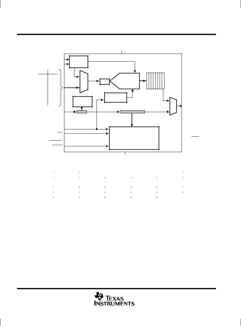
The TLC2558 and TLC2554 are a family of high-performance, 12-bit low power, 1.6 ms, CMOS analog-to-digital converters (ADC) which operate from a single 5 V power supply. These devices have three digital inputs and a 3-state output [chip select (CS), serial input-output clock (SCLK), serial data input (SDI), and serial data output (SDO)] that provide a direct 4-wire interface to the serial port of most popular host microprocessors (SPI interface). When interfaced with a DSP, a frame sync (FS) signal is used to indicate the start of a serial data frame.
In addition to a high-speed A/D converter and versatile control capability, these devices have an on-chip analog multiplexer that can select any analog inputs or one of three internal self-test voltages. The sample-and-hold function is automatically started after the fourth SCLK edge (normal sampling) or can be controlled by a special pin, CSTART, to extend the sampling period (extended sampling). The normal sampling period can also be programmed as short (12 SCLKs) or as long (24 SCLKs) to accommodate faster SCLK operation popular among high-performance signal processors. The TLC2558 and TLC2554 are designed to operate with very low power consumption. The power-saving feature is further enhanced with software/hardware/auto power down modes and programmable conversion speeds. The converter uses the external SCLK as the source of the conversion clock to achieve higher (up to 1.6 ms when a 20 MHz SCLK is used) conversion speed. There is a 4-V internal reference available. An optional external reference can also be used to achieve maximum flexibility.
Please be aware that an important notice concerning availability, standard warranty, and use in critical applications of Texas Instruments semiconductor products and disclaimers thereto appears at the end of this data sheet.
PRODUCTION DATA information is current as of publication date. Products conform to specifications per the terms of Texas Instruments standard warranty. Production processing does not necessarily include testing of all parameters.
Copyright 1999, Texas Instruments Incorporated
POST OFFICE BOX 655303 •DALLAS, TEXAS 75265 |
1 |
TLC2554, TLC2558
5-V, 12-BIT, 400 KSPS, 4/8 CHANNEL, LOW POWER,
SERIAL ANALOG-TO-DIGITAL CONVERTERS WITH AUTO POWER DOWN
SLAS220A ±JUNE 1999
functional block diagram
|
|
|
|
VCC |
|
|
|
REFP |
4 V |
|
|
|
|
|
REFM |
Reference |
|
FIFO |
|
|
|
|
|
|
|
||
|
|
|
|
|
|
|
2558 |
2554 |
|
|
12 Bit × 8 |
|
|
|
|
|
|
|
||
A0 |
A0 |
Analog MUX |
|
Low Power |
|
|
A2 |
A1 |
|
|
|
||
|
SAR ADC |
|
|
|||
A1 |
X |
|
S/H |
12-BIT |
|
|
|
|
|
|
|
||
A3 |
X |
|
|
|
|
|
A4 |
A2 |
|
|
Conversion |
|
|
A5 |
X |
|
|
|
|
|
A6 |
A3 |
Command |
|
Clock |
M |
|
A7 |
X |
Decode |
|
|
|
|
|
|
|
|
CFR |
U |
SDO |
|
SDI |
|
|
X |
|
|
|
|
|
|
|
|
|
|
|
CMR (4 MSBs) |
|
|
|
|
SCLK
CS
FS  Control Logic
  EOC/(INT) CSTART
PWDN
GND
AVAILABLE OPTIONS
|
|
PACKAGED DEVICES |
|
|
TA |
|
|
|
|
20-TSSOP |
20-SOIC |
16-SOIC |
16-TSSOP |
|
|
(PW) |
(DW) |
(D) |
(PW) |
|
|
|
|
|
0°C to 70°C |
TLC2558CPW |
TLC2558CDW |
TLC2554CD |
TLC2554CPW |
|
|
|
|
|
± 40°C to 85°C |
TLC2558IPW |
TLC2558IDW |
TLC2554ID |
TLC2554IPW |
2 |
POST OFFICE BOX 655303 •DALLAS, TEXAS 75265 |
TLC2554, TLC2558 5-V, 12-BIT, 400 KSPS, 4/8 CHANNEL, LOW POWER, SERIAL ANALOG-TO-DIGITAL CONVERTERS WITH AUTO POWER DOWN
SLAS220A ±JUNE 1999
|
|
|
|
|
|
|
|
|
|
|
|
|
|
Terminal Functions |
||||||||||||
|
|
|
|
|
|
|
|
|
|
|
|
|
|
|
|
|
|
|
|
|
|
|
|
|
|
|
|
|
|
|
|
|
|
TERMINAL |
|
|
|
|
|
|
|
|
|
|
|
|
|
|
|
|
|
|
|
|
|
|
|
|
|
|
|
|
|
|
|
|
|
|
|
|
|
|
|
|
|
|
|
|
|
|
|
NAME |
|
NO. |
|
I/O |
|
|
|
|
|
|
|
|
DESCRIPTION |
||||||||||||
|
|
TLC2554 |
TLC2558 |
|
|
|
|
|
|
|
|
|
|
|
|
|
|
|
|
|||||||
|
|
|
|
|
|
|
|
|
|
|
|
|
|
|
|
|
|
|
|
|
|
|
|
|||
|
|
|
|
|
|
|
|
|
|
|
|
|
|
|
|
|
|
|
|
|
|
|
|
|
|
|
|
A0 |
A0 |
|
6 |
|
6 |
I |
|
Analog signal inputs. The analog inputs are applied to these terminals and are internally |
|||||||||||||||||
|
A1 |
A1 |
|
7 |
|
7 |
|
|
multiplexed. The driving source impedance should be less than or equal to 1 kW. |
|||||||||||||||||
|
A2 |
A2 |
|
8 |
|
8 |
|
|
|
|
|
|
|
|
|
|
|
|
|
|
|
|
||||
|
|
|
|
For a source impedance greater than 1 kW, use the asynchronous conversion start signal CSTART |
||||||||||||||||||||||
|
A3 |
A3 |
|
9 |
|
9 |
|
|
||||||||||||||||||
|
|
|
|
|
(CSTART low time controls the sampling period) or program long sampling period to increase the |
|||||||||||||||||||||
|
|
|
A4 |
|
|
|
10 |
|
|
|||||||||||||||||
|
|
|
|
|
|
|
|
sampling time. |
||||||||||||||||||
|
|
|
A5 |
|
|
|
11 |
|
|
|||||||||||||||||
|
|
|
|
|
|
|
|
|
|
|
|
|
|
|
|
|
|
|
|
|
|
|||||
|
|
|
A6 |
|
|
|
12 |
|
|
|
|
|
|
|
|
|
|
|
|
|
|
|
|
|||
|
|
|
A7 |
|
|
|
13 |
|
|
|
|
|
|
|
|
|
|
|
|
|
|
|
|
|||
|
|
|
|
|
|
|
|
|
|
|
|
|
|
|
|
|
|
|
|
|
|
|
|
|||
|
|
|
|
|
|
|
|
16 |
|
20 |
I |
|
Chip select. A high-to-low transition on the |
|
input resets the internal 4-bit counter, enables SDI, |
|||||||||||
|
CS |
|
|
|
|
|
|
|
|
CS |
||||||||||||||||
|
|
|
|
|
|
|
|
|
|
|
|
|
and removes SDO from 3-state within a maximum setup time. SDI is disabled within a setup time |
|||||||||||||
|
|
|
|
|
|
|
|
|
|
|
|
|
after the 4-bit counter counts to 16 (clock edges) or a low-to-high transition of CS whichever |
|||||||||||||
|
|
|
|
|
|
|
|
|
|
|
|
|
happens first. SDO is 3-stated after the rising edge of |
CS. |
|
|||||||||||
|
|
|
|
|
|
|
|
|
|
|
|
|
|
|
|
|
|
|
|
|||||||
|
|
|
|
|
|
|
|
|
|
|
|
|
CS |
can be used as the FS pin when a dedicated serial port is used. |
||||||||||||
|
|
|
|
|
|
|
|
|
|
|
|
|
|
|
|
|
||||||||||
|
|
|
|
|
|
|
|
10 |
|
14 |
I |
|
This terminal controls the start of sampling of the analog input from a selected multiplex channel. |
|||||||||||||
|
CSTART |
|
|
|
|
|
||||||||||||||||||||
|
|
|
|
|
|
|
|
|
|
|
|
|
A high-to-low transition starts sampling of the analog input signal. A low-to-high transition puts the |
|||||||||||||
|
|
|
|
|
|
|
|
|
|
|
|
|
S/H in hold mode and starts the conversion. This input is independent from SCLK and works when |
|||||||||||||
|
|
|
|
|
|
|
|
|
|
|
|
|
CS is high (inactive). The low time of CSTART controls the duration of the sampling period of the |
|||||||||||||
|
|
|
|
|
|
|
|
|
|
|
|
|
converter (extended sampling). |
|||||||||||||
|
|
|
|
|
|
|
|
|
|
|
|
|
Tie this terminal to VCC if not used. |
|||||||||||||
|
|
|
|
|
|
|
|
4 |
|
4 |
O |
|
End of conversion or interrupt to host processor. |
|||||||||||||
|
EOC/(INT) |
|
|
|
|
|||||||||||||||||||||
|
|
|
|
|
|
|
|
|
|
|
|
|
[PROGRAMMED AS EOC]: This output goes from a high-to-low logic level at the end of the |
|||||||||||||
|
|
|
|
|
|
|
|
|
|
|
|
|
sampling period and remains low until the conversion is complete and data are ready for transfer. |
|||||||||||||
|
|
|
|
|
|
|
|
|
|
|
|
|
EOC is used in conversion mode 00 only. |
|||||||||||||
|
|
|
|
|
|
|
|
|
|
|
|
|
|
|
|
|
|
|||||||||
|
|
|
|
|
|
|
|
|
|
|
|
|
[PROGRAMMED AS |
INT] |
: This pin can also be programmed as an interrupt output signal to the |
|||||||||||
|
|
|
|
|
|
|
|
|
|
|
|
|
host processor. The falling edge of |
INT |
indicates data are ready for output. The following CS↓ or |
|||||||||||
|
|
|
|
|
|
|
|
|
|
|
|
|
FS↑ clears INT. The falling edge of INT puts SDO back to 3-state even if CS is still active. |
|||||||||||||
|
|
|
|
|
|
|
|
|
|
|
|
|
||||||||||||||
|
FS |
|
|
|
|
|
13 |
|
17 |
I |
|
DSP frame sync input. Indication of the start of a serial data frame in or out of the device. If FS |
||||||||||||||
|
|
|
|
|
|
|
|
|
|
|
|
|
remains low at the falling edge of |
CS, |
SDI is not enabled. A high-to-low transition on the FS input |
|||||||||||
|
|
|
|
|
|
|
|
|
|
|
|
|
resets the internal 4-bit counter and enables SDI within a maximum setup time. SDI is disabled |
|||||||||||||
|
|
|
|
|
|
|
|
|
|
|
|
|
within a setup time after the 4-bit counter counts to 16 (clock edges) or a low-to-high transition of |
|||||||||||||
|
|
|
|
|
|
|
|
|
|
|
|
|
CS whichever happens first. SDO is 3-stated after the 16th bit is presented. |
|||||||||||||
|
|
|
|
|
|
|
|
|
|
|
|
|
Tie this terminal to VCC if not used. |
|||||||||||||
|
GND |
|
|
|
|
|
11 |
|
15 |
I |
|
Ground return for the internal circuitry. Unless otherwise noted, all voltage measurements are with |
||||||||||||||
|
|
|
|
|
|
|
|
|
|
|
|
|
respect to GND. |
|||||||||||||
|
|
|
|
|
|
|
|
|
||||||||||||||||||
|
|
|
|
|
|
|
|
12 |
|
16 |
I |
|
Both analog and reference circuits are powered down when this pin is at logic zero. The device can |
|||||||||||||
|
PWDN |
|
|
|
|
|||||||||||||||||||||
|
|
|
|
|
|
|
|
|
|
|
|
|
be restarted by active CS or CSTART after this pin is pulled back to logic one. |
|||||||||||||
|
|
|
|
|
|
|
|
|
|
|
|
|
||||||||||||||
|
SCLK |
|
|
|
|
|
3 |
|
3 |
I |
|
Input serial clock. This terminal receives the serial SCLK from the host processor. SCLK is used |
||||||||||||||
|
|
|
|
|
|
|
|
|
|
|
|
|
to clock the input SDI to the input register. It is also used as the source of the conversion clock. |
|||||||||||||
|
|
|
|
|
|
|
|
|
|
|
|
|
||||||||||||||
|
SDI |
|
|
|
|
|
2 |
|
2 |
I |
|
Serial data input. The input data is presented with the MSB (D15) first. The first 4-bit MSBs, |
||||||||||||||
|
|
|
|
|
|
|
|
|
|
|
|
|
D(15±12) are decoded as one of the 16 commands (12 only for the TLC2554). All trailing blanks |
|||||||||||||
|
|
|
|
|
|
|
|
|
|
|
|
|
are filled with zeros. The configure write commands require an additional 12 bits of data. |
|||||||||||||
|
|
|
|
|
|
|
|
|
|
|
|
|
When FS is not used (FS =1), the first MSB (D15) is expected after the falling edge of CS and is |
|||||||||||||
|
|
|
|
|
|
|
|
|
|
|
|
|
shifted in on the rising edges of SCLK (after CS↓). |
|||||||||||||
|
|
|
|
|
|
|
|
|
|
|
|
|
When FS is used (typical with an active FS from a DSP) the first MSB (D15) is expected after the |
|||||||||||||
|
|
|
|
|
|
|
|
|
|
|
|
|
falling edge of FS and is shifted in on the falling edges of SCLK. |
|||||||||||||
|
|
|
|
|
|
|
|
|
|
|
|
|
|
|
|
|
|
|
|
|
|
|
|
|
|
|
POST OFFICE BOX 655303 •DALLAS, TEXAS 75265 |
3 |

TLC2554, TLC2558
5-V, 12-BIT, 400 KSPS, 4/8 CHANNEL, LOW POWER,
SERIAL ANALOG-TO-DIGITAL CONVERTERS WITH AUTO POWER DOWN
SLAS220A ±JUNE 1999
|
|
|
|
|
Terminal Functions (Continued) |
||||
|
|
|
|
|
|
|
|
|
|
|
TERMINAL |
|
|
|
|
|
|
|
|
|
|
|
|
|
|
|
|
|
|
NAME |
|
NO. |
I/O |
DESCRIPTION |
|||||
|
TLC2554 |
TLC2558 |
|
|
|
|
|
|
|
|
|
|
|
|
|
|
|
||
|
|
|
|
|
|
|
|
|
|
SDO |
|
1 |
1 |
O |
The 3-state serial output for the A/D conversion result. SDO is kept in the high-impedance state |
||||
|
|
|
|
|
when CS is high and after the CS falling edge and until the MSB (D15) is presented. The output |
||||
|
|
|
|
|
format is MSB (D15) first. |
||||
|
|
|
|
|
|
|
|
|
|
|
|
|
|
|
When FS is not used (FS = 1 at the falling edge of |
CS), the MSB (D15) is presented to the SDO |
|||
|
|
|
|
|
pin after the CS falling edge, and successive data are available at the rising edge of SCLK. |
||||
|
|
|
|
|
|
|
|
||
|
|
|
|
|
When FS is used (FS = 0 at the falling edge of |
CS), the MSB (D15) is presented to SDO after the |
|||
|
|
|
|
|
falling edge of CS and FS = 0 is detected. Successive data are available at the falling edge of SCLK. |
||||
|
|
|
|
|
(This is typically used with an active FS from a DSP.) |
||||
|
|
|
|
|
For conversion and FIFO read cycles, the first 12 bits are the result from the previous conversion |
||||
|
|
|
|
|
(data) followed by 4 trailing zeros. The first four bits from SDO for CFR read cycles should be |
||||
|
|
|
|
|
ignored. The register content is in the last 12 bits. SDO is 3 stated after the 16th bit. |
||||
|
|
|
|
|
|
||||
REFM |
|
14 |
18 |
I |
External reference input or internal reference decoupling. |
||||
|
|
|
|
|
|
||||
REFP |
|
15 |
19 |
I |
External reference input or internal reference decoupling. (Shunt capacitors of 10 μF and 0.1 μF |
||||
|
|
|
|
|
between REFP and REFM.) The maximum input voltage range is determined by the difference |
||||
|
|
|
|
|
between the voltage applied to this terminal and the REFM terminal when an external reference |
||||
|
|
|
|
|
is used. |
||||
|
|
|
|
|
|
||||
VCC |
|
5 |
5 |
I |
Positive supply voltage |
||||
detailed description
analog inputs and internal test voltages
The 4/8 analog inputs and three internal test inputs are selected by the analog multiplexer depending on the command entered. The input multiplexer is a break-before-make type to reduce input-to-input noise injection resulting from channel switching.
pseudo-differential/single-ended input
All analog inputs can be programmed as single-ended or pseudo-differential mode. Pseudo-differential mode is enabled by setting CFR.D7 ± 1. Only three analog input channels (or seven channels for TLC2558) are available for TLV2554 since one input (A1 for TLC2554 or A2 for TLC2558) is used as the MINUS input when pseudo-differential mode is used. The minus input pin can have a maximum ±0.2 V ripple. This is normally used for ground noise rejection.
converter
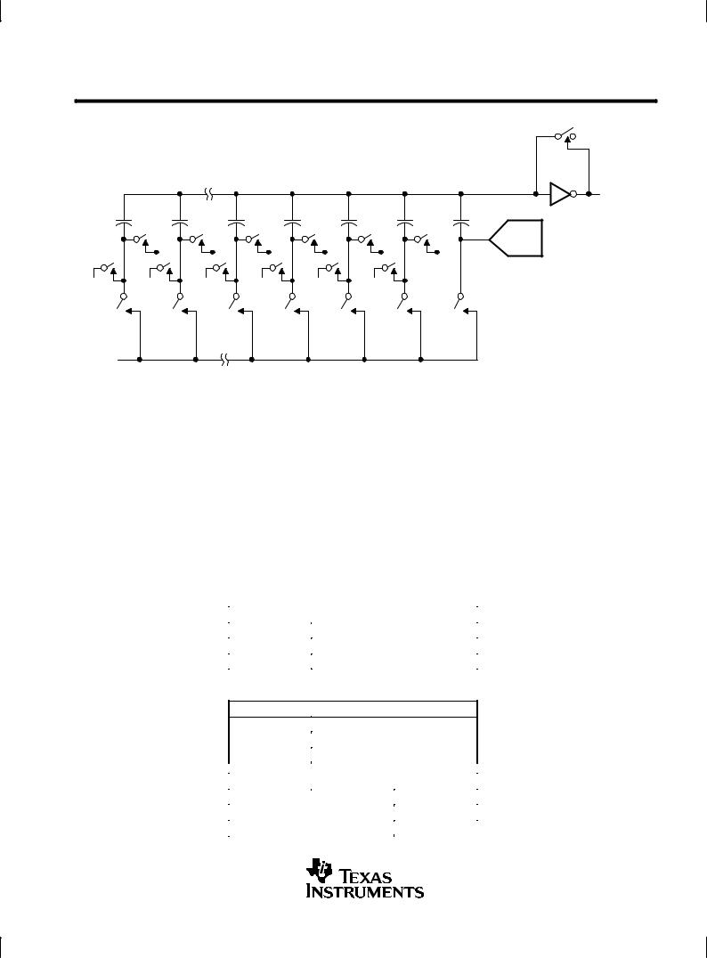
The TLC2554/58 uses a 12-bit successive approximation ADC and 2-bit resistor string. The CMOS threshold detector in the successive-approximation conversion system determines each bit by examining the charge on a series of binary-weighted capacitors (see Figure 1). In the first phase of the conversion process, the analog input is sampled by closing the SC switch and all ST switches simultaneously. This action charges all the capacitors to the input voltage.
4 |
POST OFFICE BOX 655303 •DALLAS, TEXAS 75265 |
TLC2554, TLC2558 5-V, 12-BIT, 400 KSPS, 4/8 CHANNEL, LOW POWER, SERIAL ANALOG-TO-DIGITAL CONVERTERS WITH AUTO POWER DOWN
SLAS220A ±JUNE 1999
converter (continued)
SC
Threshold
Detector
To Output
Latch
512 |
256 |
8 |
4 |
2 |
1 |
1 |
|
Node |
|
|
|
|
|
|
2-Bit |
512 |
REF+ |
REF+ |
REF+ |
REF+ |
REF+ |
REF+ |
R-String |
|
DAC |
||||||
REF± |
REF± |
REF± |
REF± |
REF± |
REF± |
|
|
|
ST |
ST |
ST |
ST |
ST |
ST |
ST |
VI
Figure 1. Simplified Model of the Successive-Approximation System
In the next phase of the conversion process the threshold detector begins identifying bits by identifying the charge (voltage) on each capacitor relative to the reference (REFM) voltage. In the switching sequence, ten capacitors are examined separately until all ten bits are identified and the charge-convert sequence is repeated. In the first step of the conversion phase, the threshold detector looks at the first capacitor (weight = 512). Node 512 of this capacitor is switched to the REFP voltage, and the equivalent nodes of all the other capacitors on the ladder are switched to REFM. If the voltage at the summing node is greater than the trip point of the threshold detector (approximately one-half the VCC voltage), a bit 0 is placed in the output register and the 512-weight capacitor is switched to REFM. If the voltage at the summing node is less than the trip point of the threshold detector, a bit 1 is placed in the register. The 512-weight capacitor remains connected to REFP through the remainder of the successive-approximation process. The process is repeated for the 1024-weight capacitor, the 128-weight capacitor, and so forth down the line until all bits are counted.
With each step of the successive-approximation process, the initial charge is redistributed among the capacitors. The conversion process relies on charge redistribution to count and weigh the bits from MSB to LSB.
serial interface
|
INPUT DATA FORMAT |
|
|
|
|
MSB |
|
LSB |
|
|
|
D15±D12 |
|
D11±D0 |
|
|
|
Command |
|
Configuration data field |
Input data is binary. All trailing blanks can be filled with zeros.
OUTPUT DATA FORMAT READ CFR
|
MSB |
|
|
|
LSB |
|
|
|
D15±D12 |
|
|
D11±D0 |
|||
|
|
|
|
|
|
|
|
|
Don't care |
|
Register content |
|
|||
|
|
|
|
||||
|
OUTPUT DATA FORMAT CONVERSION/READ FIFO |
|
|||||
|
|
|
|
|
|
|
|
|
MSB |
|
|
|
LSB |
|
|
|
|
|
|
|
|
||
|
|
D15±D4 |
|
D3±D0 |
|
|
|
|
|
|
|
|
|||
|
Conversion result |
|
All zeros |
|
|
||
|
|
|
|
|
|
|
|
|
|
|
|
|
|
|
|
POST OFFICE BOX 655303 •DALLAS, TEXAS 75265 |
5 |
TLC2554, TLC2558
5-V, 12-BIT, 400 KSPS, 4/8 CHANNEL, LOW POWER,
SERIAL ANALOG-TO-DIGITAL CONVERTERS WITH AUTO POWER DOWN
SLAS220A ±JUNE 1999
serial interface (continued)
The output data format is either binary (unipolar straight binary) or 2s complement.
binary
Zero scale code = 000h, Vcode = VREFM
Full scale code = FFFh, Vcode = VREFP ± 1 LSB
2's complement
Minus full scale code = 800h, Vcode = VREFM
Full scale code = 7FFh, Vcode = VREFP ± 1 LSB
control and timing
start of the cycle:
DWhen FS is not used ( FS = 1 at the falling edge of CS), the falling edge of CS is the start of the cycle. Input data is shifted in on the rising edge, and output data changes on the falling edge of SCLK. This is typically used for a SPI microcontroller, although it can also be used for a DSP.
DWhen FS is used ( FS is an active signal from a DSP), the falling edge of FS is the start of the cycle. Input data is shifted in on the falling edge, and output data changes on the rising edge of SCLK. This is typically used for a TMS320 DSP.
first 4-MSBs: the command register (CMR)
The TLC2554/TLC2558 have a 4-bit command set (see Table 1) plus a 12-bit configuration data field. Most of the commands require only the first 4 MSBs, i.e. without the 12-bit data field.
NOTE:
The device requires a write CFR (configuration register) with 000h data (write A000h to the serial input) at power up to initialize host select mode.
The valid commands are listed in Table 1.
Table 1. TLC2554/TLC2558 Command Set
|
SDI D(15±12) BINARY, HEX |
TLC2558 COMMAND |
TLC2554 COMMAND |
|
|
|
|
|
|
|
|
|
0000b |
0000h |
Select analog input channel 0 |
Select analog input channel 0 |
|
|
|
|
|
|
|
|
0001b |
1000h |
Select analog input channel 1 |
N/A |
|
|
|
|
|
|
|
|
0010b |
2000h |
Select analog input channel 2 |
Select analog input channel 1 |
|
|
|
|
|
|
|
|
0011b |
3000h |
Select analog input channel 3 |
N/A |
|
|
|
|
|
|
|
|
0100b |
4000h |
Select analog input channel 4 |
Select analog input channel 2 |
|
|
|
|
|
|
|
|
0101b |
5000h |
Select analog input channel 5 |
N/A |
|
|
|
|
|
|
|
|
0110b |
6000h |
Select analog input channel 6 |
Select analog input channel 3 |
|
|
|
|
|
|
|
|
0111b |
7000h |
Select analog input channel 7 |
N/A |
|
|
|
|
|
|
|
|
1000b |
8000h |
SW power down (analog + reference) |
|
|
|
|
|
|
|
|
|
1001b |
9000h |
Read CFR register data shown as SDO D(11±0) |
|
|
|
|
|
|
|
|
|
1010b |
A000h plus data |
Write CFR followed by 12-bit data |
|
|
|
|
|
|
|
|
|
1011b |
B000h |
Select test, voltage = (REFP+REFM)/2 |
|
|
|
|
|
|
|
|
|
1100b |
C000h |
Select test, voltage = REFM |
|
|
|
|
|
|
|
|
|
1101b |
D000h |
Select test, voltage = REFP |
|
|
|
|
|
|
|
|
|
1110b |
E000h |
FIFO read, FIFO contents shown as SDO D(15±4), D(3±0) = 0000 |
|
|
|
|
|
|
|
|
|
1111b |
F000h plus data |
Reserved |
|
|
|
|
|
|
|
|
|
|
|
|
|
|
|
|
|
|
|
|
6 |
POST OFFICE BOX 655303 •DALLAS, TEXAS 75265 |
TLC2554, TLC2558 5-V, 12-BIT, 400 KSPS, 4/8 CHANNEL, LOW POWER, SERIAL ANALOG-TO-DIGITAL CONVERTERS WITH AUTO POWER DOWN
SLAS220A ±JUNE 1999
control and timing (continued)
configuration
Configuration data is stored in one 12-bit configuration register (CFR) (see Table 2 for CFR bit definitions). Once configured after first power up, the information is retained in the H/W or S/W power-down state. When the device is being configured, a write CFR cycle is issued by the host processor. This is a 16-bit write. If the SCLK stops after the first 8 bits are entered, then the next eight bits can be taken after the SCLK is resumed. The status of the CFR can be read with a read CFR command.
Table 2. TLC2554/TLC2558 Configuration Register (CFR) Bit Definitions
BIT |
|
|
|
DEFINITION |
|
|
|
|
|
|
|
D(15±12) |
All zeros, nonprogrammable |
|
|
||
|
|
|
|
|
|
D11 |
Reference select |
|
|
||
|
0: External |
|
|
||
|
1: Internal |
|
|
||
|
|
|
|
|
|
D10 |
Output select |
|
|
||
|
0: Unipolar straight binary |
|
|
||
|
1: 2's complement |
|
|
||
|
|
|
|
|
|
D9 |
Sample period select |
|
|
||
|
0: Short sampling 12 SCLKs (1x sampling time) |
||||
|
1: Long sampling 24 SCLKs (2x sampling time) |
||||
|
|
|
|
|
|
D8 |
Conversion clock source select |
|
|
||
|
0: Conversion clock = SCLK |
|
|
||
|
1: Conversion clock = SCLK/2 |
|
|
||
|
|
|
|
|
|
D7 |
Input select |
|
|
||
|
0: Normal |
|
|
||
|
1: Pseudo differential CH A2(2558) or CH A1 (2554) is the differential input |
||||
|
|
|
|
|
|
D(6,5) |
Conversion mode select |
|
|
||
|
00: Single shot mode |
|
|
||
|
01: Repeat mode |
|
|
||
|
10: Sweep mode |
|
|
||
|
11: Repeat sweep mode |
|
|
||
|
|
|
|
|
|
D(4,3)² |
|
|
TLC2558 |
|
TLC2554 |
|
Sweep auto sequence select |
|
Sweep auto sequence select |
||
|
00: 0±1±2±3±4±5±6±7 |
|
00: N/A |
||
|
01: 0±2±4±6±0±2±4±6 |
|
01: 0±1±2±3±0±1±2±3 |
||
|
10: 0±0±2±2±4±4±6±6 |
|
10: 0±0±1±1±2±2±3±3 |
||
|
11: 0±2±0±2±0±2±0±2 |
|
11: 0±1±0±1±0±1±0±1 |
||
|
|
|
|
|
|
D2 |
|
|
|
|
|
EOC/INT |
± pin function select |
|
|
||
|
0: Pin used as INT |
|
|
||
|
1: Pin used as EOC |
|
|
||
|
|
||||
D(1,0) |
FIFO trigger level (sweep sequence length) |
||||
|
00: Full (INT generated after FIFO level 7 filled) |
||||
|
01: 3/4 (INT generated after FIFO level 5 filled) |
||||
|
10: 1/2 (INT generated after FIFO level 3 filled) |
||||
|
11: 1/4 (INT generated after FIFO level 1 filled) |
||||
|
|
|
|
|
|
² These bits only take effect in conversion modes 10 and 11.
sampling
The sampling period starts after the first 4 input data are shifted in if they are decoded as one of the conversion commands. These are select analog input (channel 0 through 7) and select test (channel 1 through 3).
POST OFFICE BOX 655303 •DALLAS, TEXAS 75265 |
7 |

TLC2554, TLC2558
5-V, 12-BIT, 400 KSPS, 4/8 CHANNEL, LOW POWER,
SERIAL ANALOG-TO-DIGITAL CONVERTERS WITH AUTO POWER DOWN
SLAS220A ±JUNE 1999
normal sampling
When the converter is using normal sampling, the sampling period is programmable. It can be 12 SCLKs (short sampling) or 24 SCLKs (long sampling). Long sampling helps the input analog signal sampled to settle to 0.5 LSB accuracy when input source resistance is high.
extended sampling
An asynchronous (to the SCLK) signal, via dedicated hardware pin CSTART, can be used in order to have total control of the sampling period and the start of a conversion. This is extended sampling. The falling edge of CSTART is the start of the sampling period. The rising edge of CSTART is the end of the sampling period and the start of the conversion. This function is useful for an application that requires:
DThe use of an extended sampling period to accommodate different input source impedance.
DThe use of a faster I/O clock on the serial port but not enough sampling time is available due to the fixed number of SCLKs. This could be due to a high input source impedance or due to higher MUX ON resistance at lower supply voltage (refer to application information).
Once the conversion is complete, the processor can initiate a read cycle using either the read FIFO command to read the conversion result or simply select the next channel number for conversion. Since the device has a valid conversion result in the output buffer, the conversion result is simply presented at the serial data output.
TLC2554/TLC2558 conversion modes
The TLC2554 and TLC2558 have four different conversion modes (mode 00, 01, 10, 11). The operation of each mode is slightly different, depending on how the converter performs the sampling and which host interface is used. The trigger for a conversion can be an active CSTART (extended sampling), CS (normal sampling, SPI interface), or FS (normal sampling, TMS320 DSP interface). When FS is used as the trigger, CS can be held active, i.e. CS does not need to be toggled through the trigger sequence. Different types of triggers should not be mixed throughout the repeat and sweep operations. When CSTART is used as the trigger, the conversion starts on the rising edge of CSTART. The minimum low time for CSTART is 800 ns. If an active CS or FS is used as the trigger, the conversion is started after the 16th or 28th SCLK edge. Enough time (for conversion) should be allowed between consecutive triggers so that no conversion is terminated prematurely.
one shot mode (mode 00)
One shot mode (mode 00) does not use the FIFO, and the EOC is generated as the conversion is in progress (or INT is generated after the conversion is done).
repeat mode (mode 01)
Repeat mode (mode 01) uses the FIFO. Once the programmed FIFO threshold is reached, the FIFO must be read, or the data is lost and the sequence starts over again. This allows the host to set up the converter and continue monitoring a fixed input and come back to get a set of samples when preferred. The first conversion must start with a select command so an analog input channel can be selected.
sweep mode (mode 10)
Sweep mode (mode 10) also uses the FIFO. Once it is programmed in this mode, all of the channels listed in the selected sweep sequence are visited in sequence. The results are converted and stored in the FIFO. This sweep sequence may not be completed if the FIFO threshold is reached before the list is completed. This allows the system designer to change the sweep sequence length. Once the FIFO has reached its programmed threshold, an interrupt (INT) is generated. The host must issue a read FIFO command to read and clear the FIFO before the next sweep can start.
8 |
POST OFFICE BOX 655303 •DALLAS, TEXAS 75265 |
TLC2554, TLC2558 5-V, 12-BIT, 400 KSPS, 4/8 CHANNEL, LOW POWER, SERIAL ANALOG-TO-DIGITAL CONVERTERS WITH AUTO POWER DOWN
SLAS220A ±JUNE 1999
TLC2554/TLC2558 conversion modes (continued)
repeat sweep mode (mode 11)
Repeat sweep mode (mode 11) works the same way as mode 10 except the operation has an option to continue even if the FIFO threshold is reached. Once the FIFO has reached its programmed threshold, an interrupt (INT) is generated. Then two things may happen:
1.The host may choose to act on it (read the FIFO) or ignore it. If the next cycle is a read FIFO cycle, all of the data stored in the FIFO is retained until it has been read in order.
2.If the next cycle is not a read FIFO cycle, or another CSTART is generated, all of the content stored in the FIFO is cleared before the next conversion result is stored in the FIFO, and the sweep is continued.
|
|
|
|
|
Table 3. TLC2554/TLC2558 Conversion Mode |
||||||
|
|
|
|
|
|
|
|
|
|
|
|
CONVERSION |
CFR |
SAMPLING |
|
OPERATION |
|||||||
MODE |
D(6,5) |
|
TYPE |
|
|
||||||
|
|
|
|
|
|
|
|
||||
|
|
|
|
|
|
|
|
|
|
|
|
One shot |
00 |
Normal |
|
• Single conversion from a selected channel |
|||||||
|
|
|
|
|
|
• CS or FS to start select/sampling/conversion/read |
|||||
|
|
|
|
|
|
• One INT or EOC generated after each conversion |
|||||
|
|
|
|
|
|
• Host must serve INT by selecting channel, and converting and reading the previous output. |
|||||
|
|
|
|
|
|
|
|
|
|
|
|
|
|
Extended |
|
• Single conversion from a selected channel |
|||||||
|
|
|
|
|
|
• CS to select/read |
|||||
|
|
|
|
|
|
• CSTART to start sampling and conversion |
|||||
|
|
|
|
|
|
• One INT or EOC generated after each conversion |
|||||
|
|
|
|
|
|
• Host must serve INT by selecting next channel and reading the previous output. |
|||||
|
|
|
|
|
|
|
|
|
|
|
|
Repeat |
01 |
Normal |
|
• Repeated conversions from a selected channel |
|||||||
|
|
|
|
|
|
• CS or FS to start sampling/conversion |
|||||
|
|
|
|
|
|
• One INT generated after FIFO is filled up to the threshold |
|||||
|
|
|
|
|
|
• Host must serve INT by either 1) (FIFO read) reading out all of the FIFO contents up to the |
|||||
|
|
|
|
|
|
threshold, then repeat conversions from the same selected channel or 2) writing another |
|||||
|
|
|
|
|
|
command(s) to change the conversion mode. If the FIFO is not read when INT is served, it |
|||||
|
|
|
|
|
|
is cleared. |
|||||
|
|
|
|
|
|
|
|
|
|
|
|
|
|
|
|
|
|
|
|
|
|
||
|
|
Extended |
|
• Same as normal sampling except |
CSTART |
starts each sampling and conversion when |
CS |
is |
|||
|
|
|
|
|
|
high. |
|||||
|
|
|
|
|
|
|
|
|
|||
Sweep |
10 |
Normal |
|
• One conversion per channel from a sequence of channels |
|||||||
|
|
|
|
|
|
• CS or FS to start sampling/conversion |
|||||
|
|
|
|
|
|
• One INT generated after FIFO is filled up to the threshold |
|||||
|
|
|
|
|
|
• Host must serve INT by (FIFO read) reading out all of the FIFO contents up to the threshold, |
|||||
|
|
|
|
|
|
then write another command(s) to change the conversion mode. |
|||||
|
|
|
|
|
|
|
|
|
|||
|
|
|
|
|
|
|
|
|
|||
|
|
Extended |
|
• Same as normal sampling except |
CSTART |
starts each sampling and conversion when |
CS |
is |
|||
|
|
|
|
|
|
high. |
|||||
|
|
|
|
|
|
|
|
|
|||
Repeat sweep |
11 |
Normal |
|
• Repeated conversions from a sequence of channels |
|||||||
|
|
|
|
|
|
• CS or FS to start sampling/conversion |
|||||
|
|
|
|
|
|
• One INT generated after FIFO is filled up to the threshold |
|||||
|
|
|
|
|
|
• Host must serve INT by either 1) (FIFO read) reading out all of the FIFO contents up to the |
|||||
|
|
|
|
|
|
threshold, then repeat conversions from the same selected channel or 2) writing another |
|||||
|
|
|
|
|
|
command(s) to change the conversion mode. If the FIFO is not read when INT is served it is |
|||||
|
|
|
|
|
|
cleared. |
|||||
|
|
|
|
|
|
|
|
|
|||
|
|
|
|
|
|
|
|
|
|||
|
|
Extended |
|
• Same as normal sampling except |
CSTART |
starts each sampling and conversion when |
CS |
is |
|||
|
|
|
|
|
|
high. |
|||||
|
|
|
|
|
|
|
|
|
|
|
|
NOTE: Programming the EOC/INT pin as the EOC signal works for mode 00 only. The other three modes automatically generate an INT signal irrespective of whether EOC/INT is programmed.
POST OFFICE BOX 655303 •DALLAS, TEXAS 75265 |
9 |
TLC2554, TLC2558
5-V, 12-BIT, 400 KSPS, 4/8 CHANNEL, LOW POWER,
SERIAL ANALOG-TO-DIGITAL CONVERTERS WITH AUTO POWER DOWN
SLAS220A ±JUNE 1999
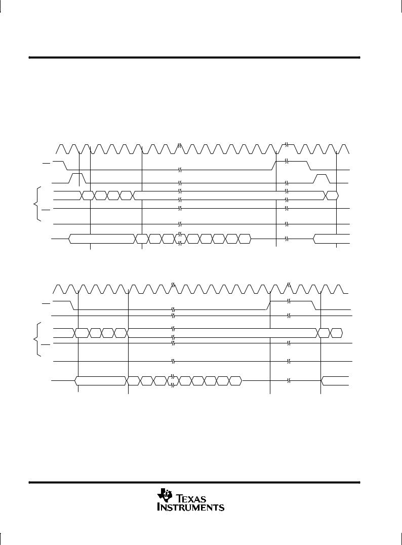
timing diagrams
The timing diagrams can be categorized into two major groups: nonconversion and conversion. The nonconversion cycles are read and write (configuration). None of these cycles carry a conversion. Conversion cycles are those four modes of conversion.
read cycle (read FIFO or read CFR)
read CFR cycle:
The read command is decoded in the first 4 clocks. SDO outputs the contents of the CFR after the 4th SCLK.
|
1 |
2 |
3 |
4 |
5 |
6 |
7 |
12 |
13 |
14 |
15 |
16 |
1 |
SCLK |
|
|
|
|
|
|
|
|
|
|
|
|
|
CS |
|
|
|
|
|
|
|
|
|
|
|
|
|
FS |
|
|
|
|
|
|
|
|
|
|
|
|
|
SDI |
ID15 |
ID14 |
ID13 |
ID12 |
|
|
|
|
|
|
|
|
ID15 |
INT |
|
|
|
|
|
|
|
|
|
|
|
|
|
EOC |
|
|
|
|
|
|
|
|
|
|
|
|
|
SDO |
|
|
|
|
OD11 OD10 |
OD9 |
OD4 |
OD3 |
OD2 |
OD1 |
OD0 |
|
|
|
|
|
|
|
|
|
|
|
|
|
|
|
|
Figure 2. TLC2554/TLC2558 Read CFR Cycle (FS active)
|
1 |
2 |
3 |
4 |
5 |
6 |
7 |
12 |
13 |
14 |
15 |
16 |
1 |
|
SCLK |
|
|
|
|
|
|
|
|
|
|
|
|
|
|
CS |
|
|
|
|
|
|
|
|
|
|
|
|
|
|
FS |
|
|
|
|
|
|
|
|
|
|
|
|
|
|
SDI |
ID15 |
ID14 |
ID13 |
ID12 |
|
|
|
|
|
|
|
|
ID15 |
ID14 |
INT |
|
|
|
|
|
|
|
|
|
|
|
|
|
|
EOC |
|
|
|
|
|
|
|
|
|
|
|
|
|
|
SDO |
|
|
|
|
OD11 |
OD10 |
OD9 |
OD4 |
OD3 |
OD2 |
OD1 |
OD0 |
|
|
|
|
|
|
|
|
|
|
|
|
|
|
|
|
Figure 3. TLC2554/TLC2558 Read CFR Cycle (FS = 1)
10 |
POST OFFICE BOX 655303 •DALLAS, TEXAS 75265 |
TLC2554, TLC2558 5-V, 12-BIT, 400 KSPS, 4/8 CHANNEL, LOW POWER, SERIAL ANALOG-TO-DIGITAL CONVERTERS WITH AUTO POWER DOWN
SLAS220A ±JUNE 1999
read cycle (read FIFO or read CFR) (continued)
FIFO read cycle
The first command in the active cycle after INT is generated, if the FIFO is used, is assumed as the FIFO read command. The first FIFO content is output immediately before the command is decoded. If this command is not a FIFO read, then the output is terminated but the first data in the FIFO is retained until a valid FIFO read command is decoded. Use of more layers of the FIFO reduces the time taken to read multiple data. This is because the read cycle does not generate EOC or INT nor does it carry out any conversion.
1 |
2 |
3 |
4 |
5 |
6 |
7 |
12 |
13 |
14 |
15 |
16 |
1 |
SCLK
CS
FS
SDI |
ID15 |
ID14 |
ID13 |
ID12 |
ID15 |
ID14 |
INT
EOC
SDO |
OD11 OD10 OD9 |
OD8 OD7 OD6 OD5 |
OD0 |
|
|
|
Figure 4. TLC2554/TLC2558 Continuous FIFO Read Cycle (FS = 1) (controlled by SCLK, SCLK can stop between each 16 SCLKs)
POST OFFICE BOX 655303 •DALLAS, TEXAS 75265 |
11 |

TLC2554, TLC2558
5-V, 12-BIT, 400 KSPS, 4/8 CHANNEL, LOW POWER,
SERIAL ANALOG-TO-DIGITAL CONVERTERS WITH AUTO POWER DOWN
SLAS220A ±JUNE 1999
write cycle (write CFR)
The write cycle is used to write to the configuration register CFR (with 12-bit register content). The write cycle does not generate an EOC or INT nor does it carry out any conversion.
|
1 |
2 |
3 |
4 |
5 |
6 |
7 |
12 |
13 |
14 |
15 |
16 |
1 |
SCLK |
|
|
|
|
|
|
|
|
|
|
|
|
|
CS |
|
|
|
|
|
|
|
|
|
|
|
|
|
FS |
|
|
|
|
|
|
|
|
|
|
|
|
|
SDI |
ID15 |
ID14 |
ID13 |
ID12 |
ID11 |
ID10 |
ID9 |
ID4 |
ID3 |
ID2 |
ID1 |
ID0 |
ID15 |
INT |
|
|
|
|
|
|
|
|
|
|
|
|
|
EOC |
|
|
|
|
|
|
|
|
|
|
|
|
|
SDO |
|
|
|
|
|
|
|
|
|
|
|
|
|
Figure 5. TLC2554/TLC2558 Write Cycle (FS active)
|
1 |
2 |
3 |
4 |
5 |
6 |
7 |
12 |
13 |
14 |
15 |
16 |
1 |
SCLK |
|
|
|
|
|
|
|
|
|
|
|
|
|
CS |
|
|
|
|
|
|
|
|
|
|
|
|
|
FS |
|
|
|
|
|
|
|
|
|
|
|
|
|
SDI |
ID15 |
ID14 |
ID13 |
ID12 |
ID11 |
ID10 |
ID9 |
ID4 |
ID3 |
ID2 |
ID1 |
ID0 |
ID15 ID14 |
INT |
|
|
|
|
|
|
|
|
|
|
|
|
|
EOC |
|
|
|
|
|
|
|
|
|
|
|
|
|
SDO |
|
|
|
|
|
|
|
|
|
|
|
|
|
Figure 6. TLC2554/TLC2558 Write Cycle (FS = 1)
12 |
POST OFFICE BOX 655303 •DALLAS, TEXAS 75265 |
 Loading...