


TLC354IDR
Texas Instruments TLC354IDR, TLC354IN, TLC354ID, TLC354CPWR, TLC354CPW Datasheet
...
1
2
3
4
5
6
7
14
13
12
11
10
9
8
1OUT
2OUT
V
DD
2IN–
2IN+
1IN–
1IN+
3OUT
4OUT
V
DD–
/GND
4IN+
4IN–
3IN+
3IN–
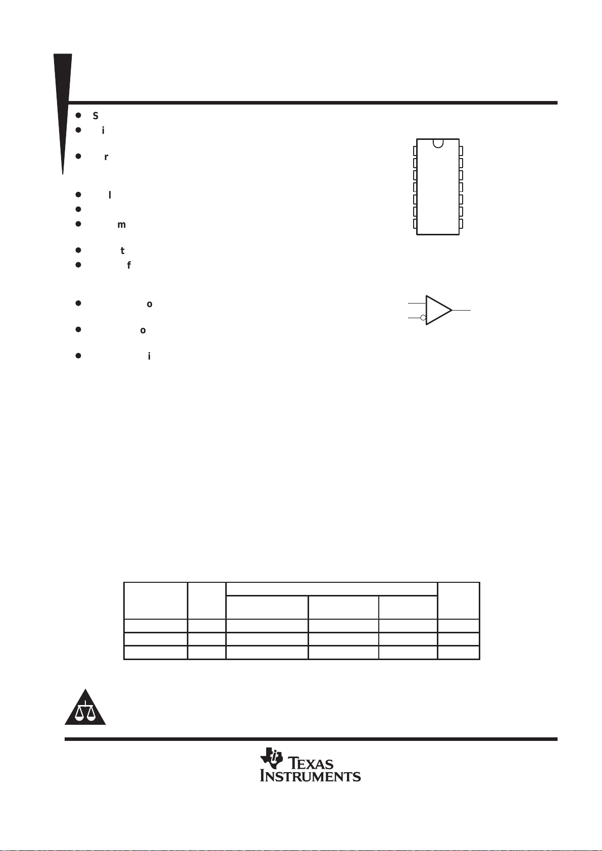
D, N, OR PW PACKAGE
(TOP VIEW)
symbol (each comparator)
IN+
IN–
OUT
TLC354
LinCMOS QUADRUPLE DIFFERENTIAL COMPARATORS
SLCS116B – SEPTEMBER 1985 – REVISED FEBRUAR Y 1997
1
POST OFFICE BOX 655303 • DALLAS, TEXAS 75265
D
Single- or Dual-Supply Operation
D
Wide Range of Supply Voltages
1.4 V to 18 V
D
Very Low Supply Current Drain
300 µA Typ at 5 V
130 µA Typ at 1.4 V
D
Built-In ESD Protection
D
High Input Impedance . . . 1012 Ω Typ
D
Extremely Low Input Blas Current
5 pA Typ
D
Ultrastable Low Input Offset Voltage
D
Input Offset Voltage Change at Worst-Case
Input Conditions Typically 0.23 µV/Month,
Including the First 30 Days
D
Common-Mode Input Voltage Range
Includes Ground
D
Outputs Compatible With TTL, MOS, and
CMOS
D
Pin-Compatible With LM339
description
This device is fabricated using LinCMOS technology and consists of four independent differential voltage
comparators; each is designed to operate from a single power supply. Operation from dual supplies is also
possible if the difference between the two supplies is 1.4 V to 18 V . Each device features extremely high input
impedance (typically greater than 10
12
Ω), which allows direct interface to high-impedance sources. The
outputs are n-channel open-drain configurations and can be connected to achieve positive-logic wired-AND
relationships. The capability of the TLC354 to operate from a 1.4-V supply makes this device ideal for
low-voltage battery applications.
The TLC354 has internal electrostatic discharge (ESD) protection circuits and has been classified with a 2000-V
ESD rating tested under MIL-STD-833C, Method 3015. However, care should be exercised in handling this
device as exposure to ESD may result in degradation of the device parametric performance.
The TLC354C is characterized for operation from 0°C to 70°C. The TLC354I is characterized for operation over
the industrial temperature range of – 40° to 85°C. The TLC354M is characterized for operation over the full
military temperature range –55°C to 125°C.
AVAILABLE OPTIONS
PACKAGED DEVICES
CHIP
T
A
V
IO
max
AT 25°C
SMALL OUTLINE
(D)
PLASTIC DIP
(P)
TSSOP
(PW)
FORM
(Y)
0°C to 70°C 5 mV TLC354CD TLC354CN TLC354CPW TLC354Y
–40°C to 85°C 5 mV TLC354ID TLC354IN — —
–55°C to 125°C 5 mV TLC354MD TLC354MN — —
The D packages are available taped and reeled. Add R suffix to device type (e.g., TLC354CDR).
Please be aware that an important notice concerning availability, standard warranty, and use in critical applications of
Texas Instruments semiconductor products and disclaimers thereto appears at the end of this data sheet.
Copyright 1997, Texas Instruments Incorporated
PRODUCTION DATA information is current as of publication date.
Products conform to specifications per the terms of Texas Instruments
standard warranty. Production processing does not necessarily include
testing of all parameters.
LinCMOS is a trademark of Texas Instruments Incorporated.
TLC354
LinCMOS QUADRUPLE DIFFERENTIAL COMPARATORS
SLCS116B – SEPTEMBER 1985 – REVISED FEBRUAR Y 1997
2
POST OFFICE BOX 655303 • DALLAS, TEXAS 75265
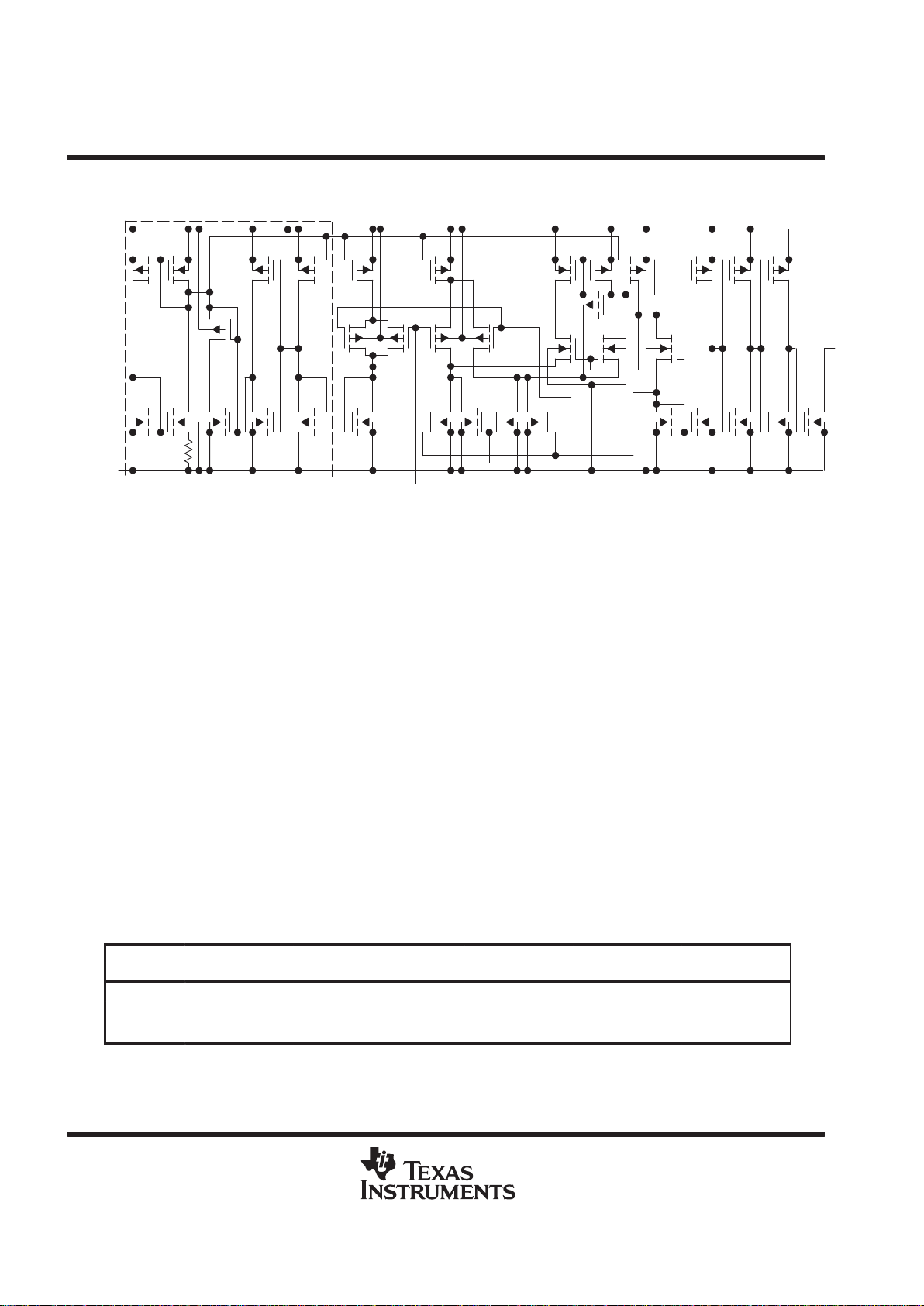
equivalent schematic (each comparator)
V
DD
V
DD–
/
GND
IN+ IN–
OUT
Common to All Channels
absolute maximum ratings over operating free-air temperature (unless otherwise noted)
†
Supply voltage, V
DD
(see Note 1) 18 V. . . . . . . . . . . . . . . . . . . . . . . . . . . . . . . . . . . . . . . . . . . . . . . . . . . . . . . . . . . .
Differential input voltage, V
ID
(see Note 2) ±18 V. . . . . . . . . . . . . . . . . . . . . . . . . . . . . . . . . . . . . . . . . . . . . . . . . .
Input voltage, V
I
V
DD
. . . . . . . . . . . . . . . . . . . . . . . . . . . . . . . . . . . . . . . . . . . . . . . . . . . . . . . . . . . . . . . . . . . . . . . . . . .
Input voltage range, V
I
–0.3 V to 18 V. . . . . . . . . . . . . . . . . . . . . . . . . . . . . . . . . . . . . . . . . . . . . . . . . . . . . . . . . . . . .
Output voltage, V
O
18 V. . . . . . . . . . . . . . . . . . . . . . . . . . . . . . . . . . . . . . . . . . . . . . . . . . . . . . . . . . . . . . . . . . . . . . . . .
Input current, I
I
±5 mA. . . . . . . . . . . . . . . . . . . . . . . . . . . . . . . . . . . . . . . . . . . . . . . . . . . . . . . . . . . . . . . . . . . . . . . . . .
Output current, I
O
20 mA. . . . . . . . . . . . . . . . . . . . . . . . . . . . . . . . . . . . . . . . . . . . . . . . . . . . . . . . . . . . . . . . . . . . . . . .
Duration of output short circuit to ground (see Note 3) Unlimited. . . . . . . . . . . . . . . . . . . . . . . . . . . . . . . . . . . . . .
Continuous total dissipation See Dissipation Rating Table. . . . . . . . . . . . . . . . . . . . . . . . . . . . . . . . . . . . . . . . . . .
Operating free-air temperature range, T
A
: TLC354C 0°C to 70°C. . . . . . . . . . . . . . . . . . . . . . . . . . . . . . . . . . . . .
TLC354I –40°C to 85°C. . . . . . . . . . . . . . . . . . . . . . . . . . . . . . . . . . . .
TLC354M –55°C to 125°C. . . . . . . . . . . . . . . . . . . . . . . . . . . . . . . . . .
Storage temperature range –65°C to 150°C. . . . . . . . . . . . . . . . . . . . . . . . . . . . . . . . . . . . . . . . . . . . . . . . . . . . . . . .
Lead temperature 1,6 mm (1/16 inch) from case for 10 seconds 260°C. . . . . . . . . . . . . . . . . . . . . . . . . . . . . . .
†
Stresses beyond those listed under “absolute maximum ratings” may cause permanent damage to the device. These are stress ratings only, and
functional operation of the device at these or any other conditions beyond those indicated under “recommended operating conditions” is not
implied. Exposure to absolute-maximum-rated conditions for extended periods may affect device reliability.
NOTES: 1. All voltage values except differential voltages are with respect to network ground.
2. Differential voltages are at IN+ with respect to IN–.
3. Short circuits from outputs to VDD can cause excessive heating and eventual device destruction.
DISSIPATION RATING TABLE
T
≤ 25°C DERATING DERATE T
= 70°C T
= 85°C T
= 125°C
PACKAGE
A
POWER RATING FACTOR ABOVE T
A
A
POWER RATINGAPOWER RATINGAPOWER RATING
D 500 mW 7.6 mW/°C 84°C 500 mW 494 mW 190 mW
N 500 mW 9.2 mW/°C96°C 500 mW 500 mW 230 mW
PW 700 mW 5.6 mW/°C 25°C 448 mW N/A N/A
TLC354
LinCMOS QUADRUPLE DIFFERENTIAL COMPARATORS
SLCS116B – SEPTEMBER 1985 – REVISED FEBRUAR Y 1997
3
POST OFFICE BOX 655303 • DALLAS, TEXAS 75265
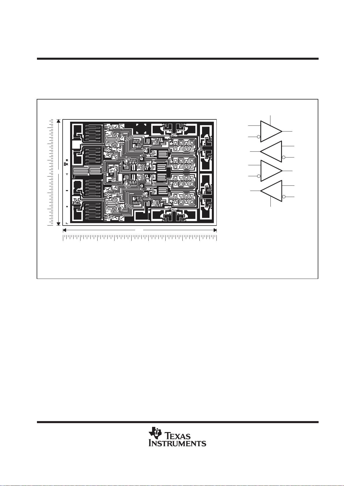
TLC364Y chip information
This chip, when properly assembled, displays characteristics similar to the TLC354C. Thermal compression or
ultrasonic bonding can be used on the doped-aluminum bonding pads. Chips can be mounted with conductive
epoxy or a gold-silicon preform.
BONDING PAD ASSIGNMENTS
CHIP THICKNESS: 15 TYPICAL
BONDING PADS: 4 × 4 MINIMUM
T
JMAX
= 150°C
TOLERANCES ARE ±10%.
ALL DIMENSIONS ARE IN MILS.
PIN (4) IS INTERNALLY CONNECTED
TO BACKSIDE OF CHIP.
+
–
3OUT
3 IN+
3IN–
V
DD–
/GND
(10)
(9)
(8)
(11)
(14)
–
+
(13)
4IN+
4IN–
4OUT
(12)
+
–
V
DD
(3)
(4)
(7)
(6)
(5)
(1)
–
+
(2)
65
90
1IN+
1IN–
2OUT
1OUT
2IN+
2IN–
(12)
(13)
(14)
(1)
(2)
(3)
(4) (5)
(6)
(7)
(8)
(9)
(10)(11)
SLCS116B – SEPTEMBER 1985 – REVISED FEBRUARY 1997
LinCMOS
QUADRUPLE DIFFERENTIAL COMPARATORS
TLC354
Template Release Date: 7–11–94
4
POST OFFICE BOX 655303 DALLAS, TEXAS 75265
•
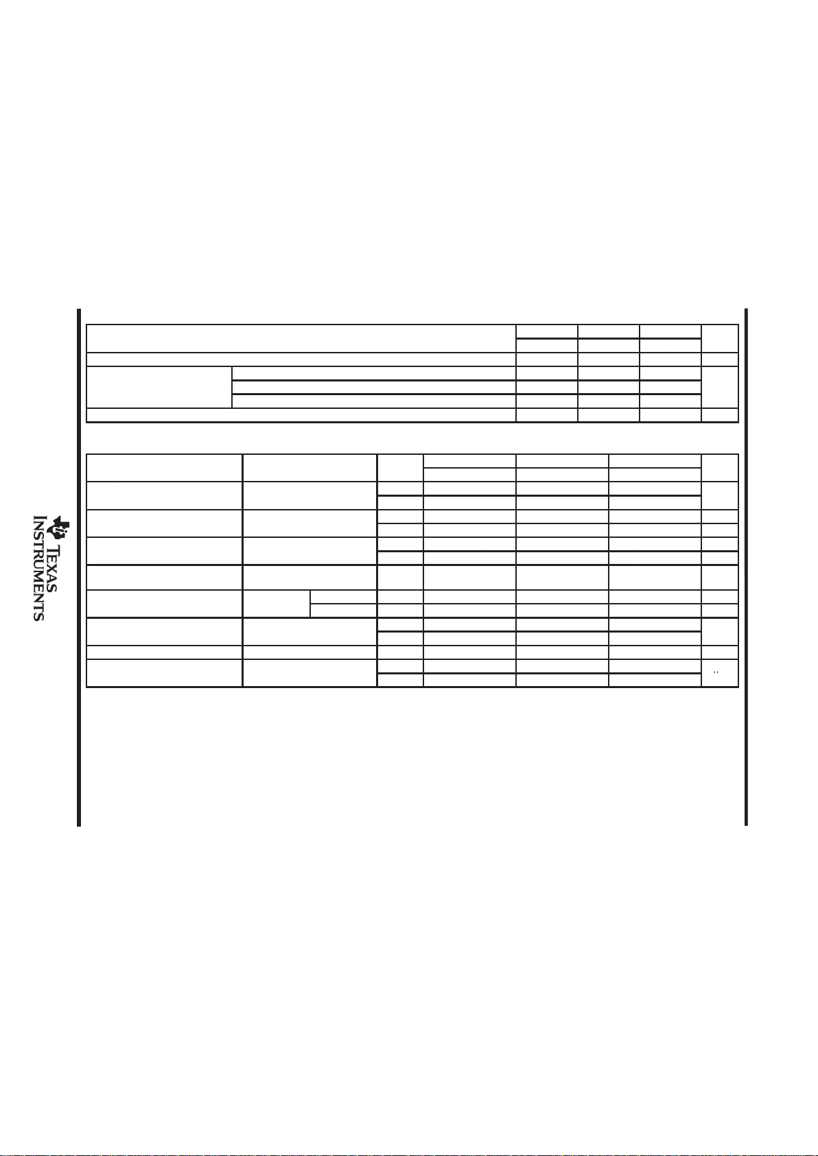
recommended operating conditions
TLC354C TLC354I TLC354M
MIN MAX MIN MAX MIN MAX
UNIT
Supply voltage, V
DD
1.4 16 1.4 16 1.4 16 V
VDD = 1.4 V 0 0.2 0 0.2 0 0.2
Common-mode input voltage, V
IC
VDD = 5 V 0 3.5 0 3.5 0 3.5
V
VDD = 10 V 0 8.5 0 8.5 0 8.5
Operating free-air temperature, T
A
0 70 –40 85 –55 125 °C
electrical characteristics at specified free-air temperature, VDD = 1.4 V
TLC354C TLC354I TLC354M
PARAMETER
TEST CONDITIONS
T
A
†
MIN TYP MAX MIN TYP MAX MIN TYP MAX
UNIT
p
25°C 2 5 2 5 2 5
VIOInput offset voltage
V
IC
=
V
ICR
min
,
See Note 4
Full range 6.5 7 10
mV
p
25°C 1 1 1 pA
IIOInput offset current
MAX 0.3 1 10 nA
p
25°C 5 5 5 pA
IIBInput bias current
MAX 0.6 2 20 nA
V
ICR
Common-mode input voltage
range
25°C
0 to
0.2
0 to
0.2
0 to
0.2
V
p
VOH = 5 V 25°C 0.1 0.1 0.1 nA
IOHHigh-level output current
V
ID
= 1
V
VOH = 15 V Full range 1 1 1 µA
p
25°C 100 200 100 200 100 200
VOLLow-level output voltage
V
ID
= –0.5 V,
I
OL
= 0.6
mA
Full range 200 200 200
mV
I
OL
Low-level output current VID = –0.5 V, VOL = 300 mV 25°C 1 1.6 1 1.6 1 1.6 mA
Supply current
25°C 130 300 130 300 130 300
I
DD
y
(four comparators)
V
ID
= 0.5 V,
No load
Full range 400 400 400
µ
A
†
All characteristics are measured with zero common-mode input voltage unless otherwise noted. Full range is 0°C to 70°C for TLC354C, –40°C to 85°C for TLC354I, and – 55°C
to 125°C for the TLC354M. MAX is 70°C for TLC354C, 85°C TLC354I, and 125°C for the TLC354M. IMPORTANT: See Parameter Measurement Information.
NOTE 4: The offset voltage limits given are the maximum values required to drive the output above 1.25 V or below 150 mV with a 10-kΩ resistor between the output and VDD. They
can be verified by applying the limit value to the input and checking for the appropriate output state.
 Loading...