


TL497AIN
Texas Instruments TL497AIN, TL497AIJ, TL497AID, TL497AIDR, TL497ACPWR Datasheet
...
TL497A
SWITCHING VOLTAGE REGULATORS
SLVS009D – JUNE 1976 – REVISED JULY 1999
1
POST OFFICE BOX 655303 • DALLAS, TEXAS 75265
D
High Efficiency . . . 60% or Greater
D
Output Current . . . 500 mA
D
Input Current Limit Protection
D
TTL-Compatible Inhibit
D
Adjustable Output Voltage
D
Input Regulation . . . 0.2% Typ
D
Output Regulation . . . 0.4% Typ
D
Soft Start-Up Capability
description
The TL497A incorporates all the active functions
required in the construction of switching voltage
regulators. It can also be used as the control
element to drive external components for high-power-output applications. The TL497A was designed for ease
of use in step-up, step-down, or voltage-inversion applications requiring high efficiency.
The TL497A is a fixed-on-time variable-frequency switching-voltage-regulator control circuit. The switch-on
time is programmed by a single external capacitor connected between FREQ CONTROL and GND. This
capacitor, CT, is charged by an internal constant-current generator to a predetermined threshold. The charging
current and the threshold vary proportionally with V
CC
. Thus, the switch-on time remains constant over the
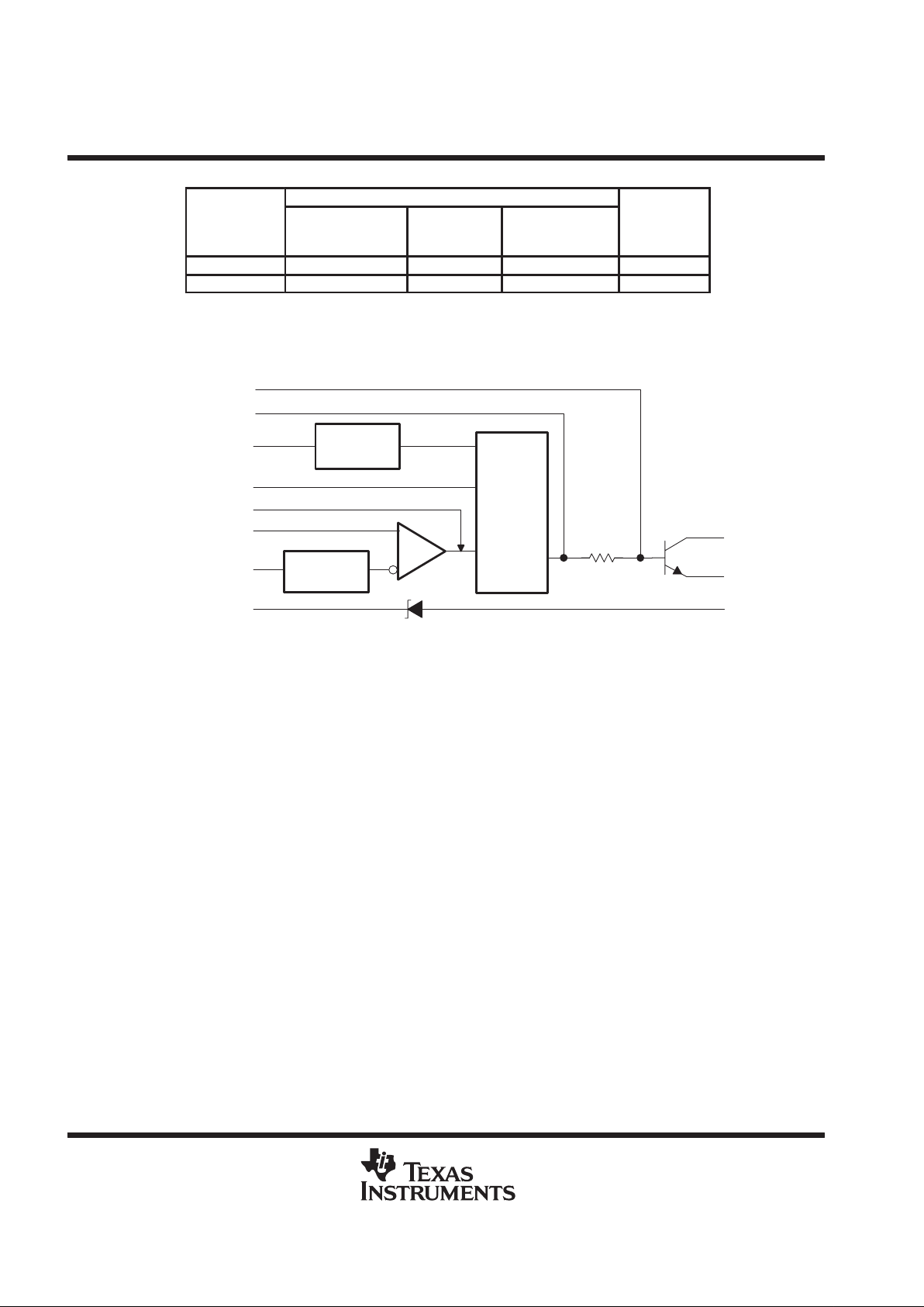
specified range of input voltage (4.5 V to 12 V). Typical on times for various values of CT are as follows:
TIMING CAPACITOR, CT (pF) 200 250 350 400 500 750 1000 1500 2000
ON TIME (µs) 19 22 26 32 44 56 80 120 180
The output voltage is controlled by an external resistor ladder network (R1 and R2 in Figures 1, 2, and 3) that
provides a feedback voltage to the comparator input. This feedback voltage is compared to the reference
voltage of 1.2 V (relative to SUBSTRA TE) by the high-gain comparator. When the output voltage decays below
the value required to maintain 1.2 V at the comparator input, the comparator enables the oscillator circuit, which
charges and discharges C
T
as described above. The internal pass transistor is driven on during the charging
of C
T
. The internal transistor can be used directly for switching currents up to 500 mA. Its collector and emitter
are uncommitted, and it is current driven to allow operation from the positive supply voltage or ground. An
internal Schottky diode matched to the current characteristics of the internal transistor also is available for
blocking or commutating purposes. The TL497A also has on-chip current-limit circuitry that senses the peak
currents in the switching regulator and protects the inductor against saturation and the pass transistor against
overstress. The current limit is adjustable and is programmed by a single sense resistor, R
CL
, connected
between VCC and CUR LIM SENS. The current-limit circuitry is activated when 0.7 V is developed across RCL.
External gating is provided by the INHIBIT input. When the INHIBIT input is high, the output is turned off.
Simplicity of design is a primary feature of the TL497A. With only six external components (three resistors, two
capacitors, and one inductor), the TL497A operates in numerous voltage-conversion applications (step-up,
step-down, invert) with as much as 85% of the source power delivered to the load. The TL497A replaces the
TL497 in all applications.
The TL497AC is characterized for operation from 0°C to 70°C. The TL497AI is characterized for operation from
–40°C to 85°C.
Copyright 1999, Texas Instruments Incorporated
PRODUCTION DATA information is current as of publication date.
Products conform to specifications per the terms of Texas Instruments
standard warranty. Production processing does not necessarily include
testing of all parameters.
Please be aware that an important notice concerning availability, standard warranty, and use in critical applications of
Texas Instruments semiconductor products and disclaimers thereto appears at the end of this data sheet.
1
2
3
4
5
6
7
14
13
12
11
10
9
8
COMP INPUT
INHIBIT
FREQ CONTROL
SUBSTRATE
GND
CATHODE
ANODE
V
CC
CUR LIM SENS
BASE DRIVE
†
BASE
†
COL OUT
NC
EMIT OUT
(TOP VIEW)
D, N, OR PW PACKAGE
NC – No internal connection
†
BASE (11) and BASE DRIVE (12) are used for device testing
only. They normally are not used in circuit applications of the
device.
TL497A
SWITCHING VOLTAGE REGULATORS
SLVS009D – JUNE 1976 – REVISED JULY 1999
2
POST OFFICE BOX 655303 • DALLAS, TEXAS 75265
AVAILABLE OPTIONS
PACKAGED DEVICES
T
A
SMALL-OUTLINE
(D)
PLASTIC DIP
(N)
SHRINK
SMALL-OUTLINE
(PW)
CHIP
FORM
(Y)
0°C to 70°C TL497ACD TL497ACN TL497ACPW TL497AY
–40°C to 85°C TL497AID TL497AIN — —
The D and PW packages are only taped and reeled. Add the suffix R to the device type (e.g.,
TL497ACPWR). Chip forms are tested at 25°C.
functional block diagram
BASE
†
11
12
BASE DRIVE
†
CUR LIM SENS
FREQ CONTROL
INHIBIT
SUBSTRATE
COMP INPUT
CATHODE
Current
Limit
Sense
13
3
2
1
4
6
1.2-V
Reference
10
8
7
COL OUT
EMIT OUT
ANODE
Oscillator
†
BASE and BASE DRIVE are used for device testing only. They normally are not used in circuit applications of the device.
TL497A
SWITCHING VOLTAGE REGULATORS
SLVS009D – JUNE 1976 – REVISED JULY 1999
3
POST OFFICE BOX 655303 • DALLAS, TEXAS 75265
absolute maximum ratings over operating free-air temperature range (unless otherwise noted)
†
Supply voltage, VCC (see Note 1) 15 V. . . . . . . . . . . . . . . . . . . . . . . . . . . . . . . . . . . . . . . . . . . . . . . . . . . . . . . . . . . .
Output voltage, VO 35 V. . . . . . . . . . . . . . . . . . . . . . . . . . . . . . . . . . . . . . . . . . . . . . . . . . . . . . . . . . . . . . . . . . . . . . . . .
Input voltage, VI(COMP INPUT) 5 V. . . . . . . . . . . . . . . . . . . . . . . . . . . . . . . . . . . . . . . . . . . . . . . . . . . . . . . . . . . . . .
Input voltage, V
I
(INHIBIT) 5 V. . . . . . . . . . . . . . . . . . . . . . . . . . . . . . . . . . . . . . . . . . . . . . . . . . . . . . . . . . . . . . . . . . . .
Diode reverse voltage 35 V. . . . . . . . . . . . . . . . . . . . . . . . . . . . . . . . . . . . . . . . . . . . . . . . . . . . . . . . . . . . . . . . . . . . . .
Power switch current 750 mA. . . . . . . . . . . . . . . . . . . . . . . . . . . . . . . . . . . . . . . . . . . . . . . . . . . . . . . . . . . . . . . . . . . .
Diode forward current 750 mA. . . . . . . . . . . . . . . . . . . . . . . . . . . . . . . . . . . . . . . . . . . . . . . . . . . . . . . . . . . . . . . . . . .
Package thermal impedance, θJA (see Notes 2 and 3): D package 86°C/W. . . . . . . . . . . . . . . . . . . . . . . . . . . .
N package 101°C/W. . . . . . . . . . . . . . . . . . . . . . . . . . .
PW package 113°C/W. . . . . . . . . . . . . . . . . . . . . . . . . .
Lead temperature 1,6 mm (1/16 inch) from case for 60 seconds 260°C. . . . . . . . . . . . . . . . . . . . . . . . . . . . . . .
Storage temperature range, T
stg
–65°C to 150°C. . . . . . . . . . . . . . . . . . . . . . . . . . . . . . . . . . . . . . . . . . . . . . . . . . .
†
Stresses beyond those listed under “absolute maximum ratings” may cause permanent damage to the device. These are stress ratings only, and
functional operation of the device at these or any other conditions beyond those indicated under “recommended operating conditions” is not
implied. Exposure to absolute-maximum-rated conditions for extended periods may affect device reliability.
NOTES: 1. All voltage values except diode voltages are with respect to network ground terminal.
2. Maximum power dissipation is a function of TJ(max),
θ
JA
, and TA. The maximum allowable power dissipation at any allowable
ambient temperature is PD = (TJ(max) – TA)/
θ
JA
. Operating at the absolute maximum TJ of 150°C can impact reliability.
3. The package thermal impedance is calculated in accordance with JESD 51, except for through-hole packages, which use a trace
length of zero.
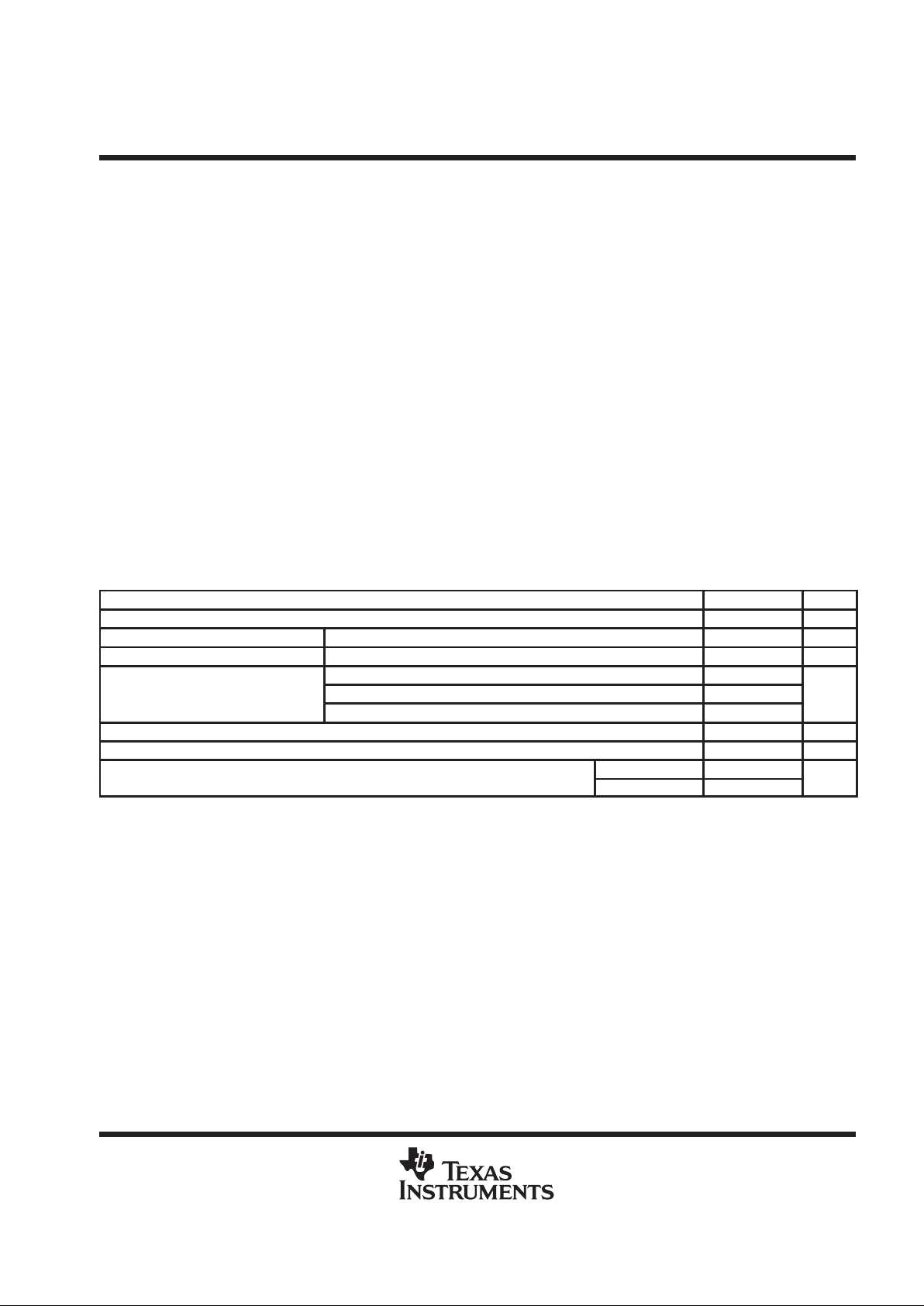
recommended operating conditions
MIN MAX UNIT
Supply voltage, V
CC
4.5 12 V
High-level input voltage, V
IH
INHIBIT pin 2.5 V
Low-level input voltage, V
IL
INHIBIT pin 0.8 V
Step-up configuration (see Figure 1) VI + 2 30
Output voltage Step-down configuration (see Figure 2) V
refVI
– 1 V
Inverting regulator (see Figure 3) –V
ref
–25
Power switch current 500 mA
Diode forward current 500 mA
p
p
TL497AC 0 70
°
O erating free-air tem erature range, T
A
TL497AI –40 85
°C
 Loading...