


Texas Instruments TL16C550CPTR, TL16C550CPT, TL16C550CPFB, TL16C550CN, TL16C550CIPT Datasheet
...TL16C550C, TL16C550CI ASYNCHRONOUS COMMUNICATIONS ELEMENT WITH AUTOFLOW CONTROL
SLLS177E ± MARCH 1994 ± REVISED APRIL1998
DProgrammable Auto-RTS and Auto-CTS
DIn Auto-CTS Mode, CTS Controls Transmitter
DIn Auto-RTS Mode, RCV FIFO Contents and Threshold Control RTS
DSerial and Modem Control Outputs Drive a RJ11 Cable Directly When Equipment Is on the Same Power Drop
DCapable of Running With All Existing TL16C450 Software
DAfter Reset, All Registers Are Identical to the TL16C450 Register Set
DUp to 16-MHz Clock Rate for Up to 1-Mbaud Operation
DIn the TL16C450 Mode, Hold and Shift Registers Eliminate the Need for Precise Synchronization Between the CPU and Serial Data
DProgrammable Baud Rate Generator Allows
Division of Any Input Reference Clock by 1 to (216 ±1) and Generates an Internal 16 ×
Clock
DStandard Asynchronous Communication Bits (Start, Stop, and Parity) Added to or Deleted From the Serial Data Stream
description
D5-V and 3.3-V Operation
DIndependent Receiver Clock Input
DTransmit, Receive, Line Status, and Data Set Interrupts Independently Controlled
DFully Programmable Serial Interface Characteristics:
±5-, 6-, 7-, or 8-Bit Characters
±Even-, Odd-, or No-Parity Bit Generation and Detection
±1-, 1 1/2-, or 2-Stop Bit Generation
±Baud Generation (dc to 1 Mbit/s)
DFalse-Start Bit Detection
DComplete Status Reporting Capabilities
D3-State Output TTL Drive Capabilities for Bidirectional Data Bus and Control Bus
DLine Break Generation and Detection
DInternal Diagnostic Capabilities:
±Loopback Controls for Communications Link Fault Isolation
±Break, Parity, Overrun, and Framing Error Simulation
DFully Prioritized Interrupt System Controls
DModem Control Functions (CTS, RTS, DSR, DTR, RI, and DCD)
The TL16C550C and the TL16C550CI are functional upgrades of the TL16C550B asynchronous communications element (ACE), which in turn is a functional upgrade of the TL16C450. Functionally equivalent to the TL16C450 on power up (character or TL16C450 mode), the TL16C550C and the TL16C550CI, like the TL16C550B, can be placed in an alternate FIFO mode. This relieves the CPU of excessive software overhead by buffering received and transmitted characters. The receiver and transmitter FIFOs store up to 16 bytes including three additional bits of error status per byte for the receiver FIFO. In the FIFO mode, there is a selectable autoflow control feature that can significantly reduce software overload and increase system efficiency by automatically controlling serial data flow using RTS output and CTS input signals.
The TL16C550C and TL16C550CI perform serial-to-parallel conversions on data received from a peripheral device or modem and parallel-to-serial conversion on data received from its CPU. The CPU can read the ACE status at any time. The ACE includes complete modem control capability and a processor interrupt system that can be tailored to minimize software management of the communications link.
Both the TL16C550C and the TL16C550CI ACE include a programmable baud rate generator capable of dividing a reference clock by divisors from 1 to 65535 and producing a 16× reference clock for the internal transmitter logic. Provisions are included to use this 16×clock for the receiver logic. The ACE accommodates a 1-Mbaud serial rate (16-MHz input clock) so that a bit time is 1 ms and a typical character time is 10 ms (start bit, 8 data bits, stop bit).
Two of the TL16C450 terminal functions on the TL16C550C and the TL16C550CI have been changed to TXRDY and RXRDY, which provide signaling to a DMA controller.
Please be aware that an important notice concerning availability, standard warranty, and use in critical applications of Texas Instruments semiconductor products and disclaimers thereto appears at the end of this data sheet.
PRODUCTION DATA information is current as of publication date. Products conform to specifications per the terms of Texas Instruments standard warranty. Production processing does not necessarily include testing of all parameters.
Copyright 1998, Texas Instruments Incorporated
POST OFFICE BOX 655303 •DALLAS, TEXAS 75265 |
1 |

TL16C550C, TL16C550CI
ASYNCHRONOUS COMMUNICATIONS ELEMENT
WITH AUTOFLOW CONTROL
SLLS177E ± MARCH 1994 ± REVISED APRIL1998
|
|
|
|
N PACKAGE |
|
|
|
|
|
|
|
|
|
|
|
|
|
|
|
|
|
|
|
|
|
|
|
|
|
|
|
|
|
|
|
FN PACKAGE |
|
|
|
|
|
|
|
|
|
|
|
|
||||||||||||||||||||
|
|
|
|
|
(TOP VIEW) |
|
|
|
|
|
|
|
|
|
|
|
|
|
|
|
|
|
|
|
|
|
|
|
|
|
|
|
|
|
|
|
|
(TOP VIEW) |
|
|
|
|
|
|
|
|
|
|
|
|
||||||||||||||||||
|
|
D0 |
|
|
|
|
|
VCC |
|
|
|
|
|
|
|
|
|
|
|
|
|
|
|
|
|
|
|
|
|
|
|
|
|
|
|
|
|
|
|
|
|
|
|
|
|
|
|
|
|
|
|
|
DCD |
|
DSR |
|
CTS |
|
|
|
|
|||||||
|
|
|
1 |
40 |
|
|
|
|
|
|
|
|
|
|
|
|
|
|
|
|
|
|
|
|
|
|
|
D4 |
D3 |
D2 |
D1 |
D0 |
|
NC |
V RI |
|
|
|
|
|
|
|
||||||||||||||||||||||||||
|
|
|
|
|
|
|
|
|
|
|
|
|
|
|
|
|
|
|
|
|
|
|
|
|
|
|
|
|
|
|
|
|
|
|||||||||||||||||||||||||||||||||||
|
|
D1 |
|
2 |
39 |
|
RI |
|
|
|
|
|
|
|
|
|
|
|
|
|
|
|
|
|
|
|
|
|
|
|
|
|
|
|
|
|
|
|
|
|||||||||||||||||||||||||||||
|
|
D2 |
|
|
|
|
|
|
|
|
|
|
|
|
|
|
|
|
|
|
|
|
|
|
|
|
|
|
|
|
|
|
|
|
|
|
|
|
|
|
|
|
|
|
|
|
|
|
|
CC |
|
|
|
|
|
|
|
|
|
|
|
|
|
|
|
|||
|
|
|
3 |
38 |
|
|
DCD |
|
|
|
|
|
|
|
|
|
|
|
|
|
|
|
|
|
|
|
|
|
|
|
|
|
|
|
|
|
|
|
|
|
|
|
|
|
|
|
|
|
|
|
|
|
|
|
|
|
|
|
|
|
|
|
|
|||||
|
|
|
|
|
|
|
|
|
|
|
|
|
|
|
|
|
|
|
|
|
|
|
|
|
|
|
|
6 |
|
5 |
|
4 |
|
3 |
|
2 |
1 |
|
44 43 42 41 40 |
|
|
|
|
|
|
|||||||||||||||||||||||
|
|
D3 |
|
4 |
37 |
|
DSR |
|
|
|
|
|
|
|
|
|
|
|
|
|
|
|
|
|
|
D5 |
7 |
|
|
|
|
|
|
|
|
|
|
|
|
|
|
|
|
|
|
|
|
|
|
|
|
|
39 |
|
|
MR |
||||||||||||
|
|
D4 |
|
5 |
36 |
|
CTS |
|
|
|
|
|
|
|
|
|
|
|
|
|
|
|
|
|
|
D6 |
8 |
|
|
|
|
|
|
|
|
|
|
|
|
|
|
|
|
|
|
|
|
|
|
|
|
|
38 |
|
|
OUT1 |
|
|||||||||||
|
|
|
|
|
|
|
|
|
|
|
|
|
|
|
|
|
|
|
|
|
|
|
|
|
|
|
|
|
|
|
|
|
|
|
|
|
|
|
|
|
|
|
|
|
|
|
|
|
||||||||||||||||||||
|
|
D5 |
|
6 |
35 |
|
MR |
|
|
|
|
|
|
|
|
|
|
|
|
|
|
|
|
|
|
D7 |
9 |
|
|
|
|
|
|
|
|
|
|
|
|
|
|
|
|
|
|
|
|
|
|
|
|
|
37 |
|
|
DTR |
|
|||||||||||
|
|
D6 |
|
7 |
34 |
|
OUT1 |
|
|
|
|
|
|
|
|
|
|
|
|
|
|
|
RCLK |
10 |
|
|
|
|
|
|
|
|
|
|
|
|
|
|
|
|
|
|
|
|
|
|
|
|
36 |
|
|
RTS |
|
|||||||||||||||
|
|
|
|
|
|
|
|
|
|
|
|
|
|
|
|
|
|
|
|
|
|
|
|
|
|
|
|
|
|
|
|
|
|
|
|
|
|
|
|
|
|
|
|
|
||||||||||||||||||||||||
|
|
D7 |
|
8 |
33 |
|
DTR |
|
|
|
|
|
|
|
|
|
|
|
|
|
|
|
|
|
|
|
|
|
|
|
|
|
|
|
|
|
|
|
|
|
|
|
|
|
|
|
|
|
|
|
|
|
|
|
|
|
|
|
|
|
|
|||||||
|
|
|
|
|
|
|
|
|
|
|
|
|
|
|
|
|
|
|
|
|
SIN |
11 |
|
|
|
|
|
|
|
|
|
|
|
|
|
|
|
|
|
|
|
|
|
|
|
|
35 |
|
|
OUT2 |
|
|||||||||||||||||
RCLK |
|
9 |
32 |
|
RTS |
|
|
|
|
|
|
|
|
|
|
|
|
|
|
|
|
|
|
NC |
|
|
|
|
|
|
|
|
|
|
|
|
|
|
|
|
|
|
|
|
|
|
|
|
|
|
34 |
|
|
NC |
||||||||||||||
|
|
|
|
|
|
|
|
|
|
|
|
|
|
|
|
|
|
|
|
12 |
|
|
|
|
|
|
|
|
|
|
|
|
|
|
|
|
|
|
|
|
|
|
|
|
|
|
||||||||||||||||||||||
|
|
SIN |
|
10 |
31 |
|
OUT2 |
|
|
|
|
|
|
|
|
|
|
|
|
|
|
|
SOUT |
13 |
|
|
|
|
|
|
|
|
|
|
|
|
|
|
|
|
|
|
|
|
|
|
|
|
33 |
|
|
INTRPT |
||||||||||||||||
SOUT |
|
11 |
30 |
|
INTRPT |
|
|
|
|
|
|
|
|
|
|
CS0 |
14 |
|
|
|
|
|
|
|
|
|
|
|
|
|
|
|
|
|
|
|
|
|
|
|
|
32 |
|
|
RXRDY |
|||||||||||||||||||||||
|
|
CS0 |
|
12 |
29 |
|
RXRDY |
|
|
|
|
|
|
|
|
|
|
|
|
|
CS1 |
|
15 |
|
|
|
|
|
|
|
|
|
|
|
|
|
|
|
|
|
|
|
|
|
|
|
|
31 |
|
|
A0 |
|||||||||||||||||
|
|
|
|
|
|
|
|
|
|
|
|
|
|
|
|
|
|
|
|
|
|
|
|
|
|
|
|
|
|
|
|
|
|
|
|
|
|
|
|
|
|
|
||||||||||||||||||||||||||
|
|
CS1 |
|
13 |
28 |
|
A0 |
|
|
|
|
|
|
|
|
|
|
|
|
|
|
|
|
|
CS2 |
16 |
|
|
|
|
|
|
|
|
|
|
|
|
|
|
|
|
|
|
|
|
|
|
|
|
30 |
|
|
A1 |
||||||||||||||
|
|
CS2 |
|
|
14 |
27 |
|
A1 |
|
|
|
|
|
|
|
|
|
|
|
|
|
|
|
|
|
|
|
|
|
17 |
|
|
|
|
|
|
|
|
|
|
|
|
|
|
|
|
|
|
|
|
|
|
|
|
|
|
|
|
|
A2 |
||||||||
|
|
|
|
|
|
|
|
|
|
|
|
|
|
|
|
|
BAUDOUT |
|
|
|
|
|
|
|
|
|
|
|
|
|
|
|
|
|
|
|
|
|
|
|
|
|
29 |
|
|
|||||||||||||||||||||||
BAUDOUT |
|
|
15 |
26 |
|
A2 |
|
|
|
|
|
|
|
|
|
|
|
|
|
|
|
|
|
|
|
|
|
|
|
18 19 20 21 |
22 23 24 25 26 27 28 |
|
|
|
|
|
|
|||||||||||||||||||||||||||||||
|
|
|
|
|
|
|
|
|
|
|
|
|
|
|
|
|
|
|
|
|
|
|
|
|
|
|
|
|
|
|
|
|||||||||||||||||||||||||||||||||||||
|
|
XIN |
|
16 |
25 |
|
|
ADS |
|
|
|
|
|
|
|
|
|
|
|
|
|
|
|
|
|
|
|
|
|
|
|
|
|
|
|
|
|
|
|
|
|
|
|
|
|
|
|
|
|
|
|
|
|
|
|
|
|
|
|
|
|
|
|
|
||||
|
|
|
|
|
|
|
|
|
|
|
|
|
|
|
|
|
|
|
|
|
|
|
|
|
|
|
XIN |
XOUT |
WR1 |
WR2 |
SS |
|
NC |
RD1 RD2 |
DDIS |
|
TXRDY |
|
ADS |
|
|
|
|
|||||||||||||||||||||||||
XOUT |
|
17 |
24 |
|
TXRDY |
|
|
|
|
|
|
|
|
|
|
|
|
|
|
|
V |
|
|
|
|
|
|
|
||||||||||||||||||||||||||||||||||||||||
|
|
|
|
|
|
|
|
|
|
|
|
|
|
|
|
|
|
|
|
|
|
|
|
|
|
|
|
|
|
|
|
|
|
|
|
|
|
|
|
|
|
|
|
|
|
|
|
|
|
|
||||||||||||||||||
|
WR1 |
|
|
18 |
23 |
|
DDIS |
|
|
|
|
|
|
|
|
|
|
|
|
|
|
|
|
|
|
|
|
|
|
|
|
|
|
|
|
|
|
|
|
|
|
|
|
|
|
|
|
|
|
|
|
|
|
|
|
|
||||||||||||
|
|
|
|
|
|
|
|
|
|
|
|
|
|
|
|
|
|
|
|
|
|
|
|
|
|
|
|
|
|
|
|
|
|
|
|
|
|
|
|
|
|
|
|
|
|
|
|
|
|
|
|
|
||||||||||||||||
WR2 |
|
19 |
22 |
|
RD2 |
|
|
|
|
|
|
|
|
|
|
|
|
|
|
|
|
|
|
|
|
|
|
|
|
|
|
|
|
|
|
|
|
|
|
|
|
|
|
|
|
|
|
|
|
|
|
|
|
|
|
|
|
|
|
|
|
|||||||
|
|
|
|
|
|
|
|
|
|
|
|
|
|
|
|
|
|
|
|
|
|
|
|
|
|
|
|
|
|
|
|
|
|
|
|
|
|
|
|
|
|
|
|
|
|
|
|
|
|
|
|
|
|
|
|
|
|
|||||||||||
|
|
|
|
|
|
|
|
|
|
|
|
|
|
|
|
|
|
|
|
|
|
|
|
|
|
|
|
|
|
|
|
|
|
|
|
|
|
|
|
|
|
|
|
|
|
|
|
|
|
|
|
|
|
|
|
|
|
|||||||||||
|
|
VSS |
|
20 |
21 |
|
RD1 |
|
|
|
|
|
|
|
|
|
|
PT/PFB PACKAGE |
|
|
|
|
|
|
|
|
|
|
|
|
|
|
|
|
|
|
|
|
|
|
|
|
|
|
|
|
|
|
|
|
|
|||||||||||||||||
|
|
|
|
|
|
|
|
|
|
|
|
|
|
|
|
|
|
|
|
|
|
|
|
|
|
|
|
|
|
|
|
|
|
|
|
|
|
|
|
|
|
|
|
|
|
|
||||||||||||||||||||||
|
|
|
|
|
|
|
|
|
|
|
|
|
|
|
|
|
|
|
|
|
|
|
|
|
|
|
|
|
|
|
|
|
|
|
|
|
|
|
|
|
|
|
|
|
|
|
|
|
|
|
|
|
|
|
|
|||||||||||||
|
|
|
|
|
|
|
|
|
|
|
|
|
|
|
|
|
|
|
|
|
|
|
|
|
|
|
|
|
|
|
|
|
|
|
|
|
|
|
|
|
|
|
|
|
|
|
|
|
|
|
|
|
|
|
|
|||||||||||||
|
|
|
|
|
|
|
|
|
|
|
|
|
|
|
|
|
|
|
|
|
|
|
|
|
|
|
(TOP VIEW) |
|
|
|
|
|
|
|
|
|
|
|
|
|
|
|
|
|
|
|
|
|
|
|
|
|
|
|
|
|
|
|
|
|
|
|
||||||
|
|
|
|
|
|
|
|
|
|
|
|
|
|
|
|
|
|
NC |
D4 D3 |
|
D2 |
D1 |
|
D0 V RI |
DCD |
DSR |
|
CTS |
|
NC |
|
|
|
|
|
|
|
|
|
|
|
|
|
|
|
|
|
|
|
|
|
|
|
|
|
|||||||||||||
|
|
|
|
|
|
|
|
|
|
|
|
|
|
|
|
|
|
|
|
|
|
|
|
|
|
|
|
|
|
|
CC |
|
|
|
|
|
|
|
|
|
|
|
|
|
|
|
|
|
|
|
|
|
|
|
|
|
|
|
|
|
|
|
|
|
|
|
|
|
|
|
|
|
|
|
|
|
|
|
|
|
|
|
|
|
|
|
|
|
|
|
|
|
|
|
|
|
|
|
|
|
|
|
|
|
|
|
|
|
|
|
|
|
|
|
|
|
|
|
|
|
|
|
|
|
|
|
|
|
|||||||||
|
|
|
|
|
|
|
|
|
|
|
|
|
|
|
|
|
|
|
|
|
|
|
|
|
|
|
|
|
|
|
|
|
|
|
|
|
|
|
|
|
|
|
|
|
|
|
|
|
|
|
|
|
|
|
|
|
|
|
|
|
|
|
|
|
|
|
|
|
|
|
|
|
|
|
|
|
|
|
|
|
|
|
|
|
|
|
|
|
|
|
|
|
|
|
|
|
|
|
|
|
|
|
|
|
|
|
|
|
|
|
|
|
|
|
|
|
|
|
|
|
|
|
|
|
|
|
|
|
|
|
|
|
|
|
|
|
|
|
|
|
|
|
|
|
|
|
|
|
|
|
48 47 46 |
45 44 43 42 41 40 39 38 37 |
|
|
|
|
NC |
|
|
|
|
|
|
|
|
|
|
|
|
|||||||||||||||||||||||||||||||||||||
|
|
|
|
|
|
|
|
|
|
|
|
|
|
|
|
|
|
|
|
|
|
|
|
|
|
|
|
|
||||||||||||||||||||||||||||||||||||||||
|
|
|
|
|
|
|
|
|
|
|
|
|
|
|
|
|
|
|
|
|
|
|
|
|
|
|
|
|
|
|
|
|
|
|
|
|
|
|
|
|
|
|
|
|
|
|
|
|
|
|
|
|
|
|
||||||||||||||
|
|
|
|
|
|
|
|
NC |
|
1 |
|
|
|
|
|
|
|
|
|
|
|
|
|
|
|
|
|
|
|
|
|
|
|
|
|
|
|
|
36 |
|
|
|
|
|
|
|
|
|
|
|
|
|
|
|
||||||||||||||
|
|
|
|
|
|
|
|
|
|
|
|
|
|
|
|
|
|
|
|
|
|
|
|
|
|
|
|
|
|
|
|
|
|
|
|
|
|
|
|
|
|
MR |
|
|
|
|
|
|
|
|
|
|
|
|
||||||||||||||
|
|
|
|
|
|
|
|
D5 |
|
2 |
|
|
|
|
|
|
|
|
|
|
|
|
|
|
|
|
|
|
|
|
|
|
|
|
|
|
|
|
35 |
|
|
|
|
|
|
|
|
|
|
|
|
|
|
|
||||||||||||||
|
|
|
|
|
|
|
|
|
|
|
|
|
|
|
|
|
|
|
|
|
|
|
|
|
|
|
|
|
|
|
|
|
|
|
|
|
|
|
|
|
|
|
|
|
|
|
|
|
|
|
|
|
|
|
|
|
|
|
|
|
|
|
|
|
|
|
|
|
|
|
|
|
|
|
|
|
D6 |
|
3 |
|
|
|
|
|
|
|
|
|
|
|
|
|
|
|
|
|
|
|
|
|
|
|
|
|
|
|
|
34 |
|
|
|
OUT1 |
|
|
|
|
|
|
|
|
|
|
|
|
|
|
|
||||||||||
|
|
|
|
|
|
|
|
|
|
|
|
|
|
|
|
|
|
|
|
|
|
|
|
|
|
|
|
|
|
|
|
|
|
|
|
|
|
|
|
|
|
|
|
|
|
|
|
|
|
|
|
|
|
|
|
|
|
|
|
|
|
|
|
|
|
|
|
|
|
|
|
|
|
|
|
|
D7 |
|
4 |
|
|
|
|
|
|
|
|
|
|
|
|
|
|
|
|
|
|
|
|
|
|
|
|
|
|
|
|
33 |
|
|
|
DTR |
|
|
|
|
|
|
|
|
|
|
|
|
|
|
|
|
|||||||||
|
|
|
|
|
|
|
|
|
|
|
|
|
|
|
|
|
|
|
|
|
|
|
|
|
|
|
|
|
|
|
|
|
|
|
|
|
|
|
|
|
|
|
|
|
|
|
|
|
|
|
|
|
|
|
|
|
|
|
|
|
|
|
|
|
|
|
|
|
|
|
|
|
|
|
|
RCLK |
|
5 |
|
|
|
|
|
|
|
|
|
|
|
|
|
|
|
|
|
|
|
|
|
|
|
|
|
|
|
|
32 |
|
|
|
RTS |
|
|
|
|
|
|
|
|
|
|
|
|
|
|
|
|
|
|||||||||
|
|
|
|
|
|
|
|
|
|
|
|
|
|
|
|
|
|
|
|
|
|
|
|
|
|
|
|
|
|
|
|
|
|
|
|
|
|
|
|
|
|
|
|
|
|
|
|
|
|
|
|
|
|
|
|
|
|
|
|
|
|
|
|
|
|
|
|
|
|
|
|
|
|
|
|
|
NC |
|
6 |
|
|
|
|
|
|
|
|
|
|
|
|
|
|
|
|
|
|
|
|
|
|
|
|
|
|
|
|
31 |
|
|
|
OUT2 |
|
|
|
|
|
|
|
|
|
|
|
|
|
|
|
||||||||||
|
|
|
|
|
|
|
|
|
|
|
|
|
|
|
|
|
|
|
|
|
|
|
|
|
|
|
|
|
|
|
|
|
|
|
|
|
|
30 |
|
|
|
INTRPT |
|
|
|
|
|
|
|
|
|
|
|
|
||||||||||||||
|
|
|
|
|
|
|
|
SIN |
|
7 |
|
|
|
|
|
|
|
|
|
|
|
|
|
|
|
|
|
|
|
|
|
|
|
|
|
|
|
|
|
|
|
|
|
|
|
|
|
|
|
|
|
|
|
|||||||||||||||
|
|
|
|
|
|
|
|
|
|
|
|
|
|
|
|
|
|
|
|
|
|
|
|
|
|
|
|
|
|
|
|
|
|
|
|
|
|
|
|
|
|
|
|
|
|
|
|
|
|
|
|
|
|
|
|
|
|
|
|
|
|
|
|
|
|
|
|
|
|
|
|
|
|
|
|
SOUT |
|
8 |
|
|
|
|
|
|
|
|
|
|
|
|
|
|
|
|
|
|
|
|
|
|
|
|
|
|
|
|
29 |
|
|
|
RXRDY |
|
|
|
|
|
|
|
|
|
|
|
|
|
|
||||||||||||
|
|
|
|
|
|
|
|
|
|
|
|
|
|
|
|
|
|
|
|
|
|
|
|
|
|
|
|
|
|
|
|
|
|
|
|
|
|
28 |
|
|
|
A0 |
|
|
|
|
|
|
|
|
|
|
|
|
|
|
|
|
|
|
||||||||
|
|
|
|
|
|
|
|
CS0 |
|
9 |
|
|
|
|
|
|
|
|
|
|
|
|
|
|
|
|
|
|
|
|
|
|
|
|
|
|
|
|
|
|
|
|
|
|
|
|
|
|
|
|
|
|
|
|
|
|
|
|
|
|||||||||
|
|
|
|
|
|
|
|
|
|
|
|
|
|
|
|
|
|
|
|
|
|
|
|
|
|
|
|
|
|
|
|
|
|
|
|
|
|
27 |
|
|
|
A1 |
|
|
|
|
|
|
|
|
|
|
|
|
|
|
|
|
|
|
||||||||
|
|
|
|
|
|
|
|
CS1 |
|
10 |
|
|
|
|
|
|
|
|
|
|
|
|
|
|
|
|
|
|
|
|
|
|
|
|
|
|
|
|
|
|
|
|
|
|
|
|
|
|
|
|
|
|
|
|
|
|
|
|
|
|||||||||
|
|
|
|
|
|
|
|
|
|
|
|
|
|
|
|
|
|
|
|
|
|
|
|
|
|
|
|
|
|
|
|
|
|
|
|
|
|
|
|
|
|
|
|
26 |
|
|
|
A2 |
|
|
|
|
|
|
|
|
|
|
|
|
|
|
|
|
|
|
||
|
|
|
|
|
|
|
|
CS2 |
|
|
11 |
|
|
|
|
|
|
|
|
|
|
|
|
|
|
|
|
|
|
|
|
|
|
|
|
|
|
|
|
|
|
|
|
|
|
|
|
|
|
|
|
|
|
|
|
|
|
|
|
|
||||||||
|
|
|
|
|
|
|
|
|
|
|
|
|
|
|
|
|
|
|
|
|
|
|
|
|
|
|
|
|
|
|
|
|
|
|
|
|
|
|
|
|
|
|
|
25 |
|
|
|
NC |
|
|
|
|
|
|
|
|
|
|
|
|
||||||||
|
|
|
|
|
|
|
BAUDOUT |
|
|
12 |
|
|
|
|
|
|
|
|
|
|
|
|
|
|
|
|
|
|
|
|
|
|
|
|
|
|
|
|
|
|
|
|
|
|
|
|
|
|
|
|
|
|
|
|||||||||||||||
|
|
|
|
|
|
|
|
|
|
|
|
|
13 |
|
14 15 16 17 18 19 20 21 22 23 24 |
|
|
|
|
|
|
|
|
|
|
|
|
|
|
|
|
|
|
|
|
|
|
|
|
|||||||||||||||||||||||||||||
|
|
|
|
|
|
|
|
|
|
|
|
|
|
|
|
|
|
|
|
|
|
|
|
|
|
|
|
|
|
|
|
|
|
|
|
|
||||||||||||||||||||||||||||||||
|
|
|
|
|
|
|
|
|
|
|
|
|
|
|
|
|
|
|
|
|
|
|
|
|
|
|
|
|
|
|
|
|
|
|
|
|
|
|
|
|
|
|
|
|
|
|
|
|
|
|
|
|
|
|
|
|
|
|
|
|
|
|
|
|||||
|
|
|
|
|
|
|
|
|
|
|
|
|
|
|
|
|
|
NC |
XIN XOUT |
|
WR1 |
WR2 |
V RD1 RD2 |
NC |
DDIS |
|
TXRDY |
|
ADS |
|
|
|
|
|
|
|
|
|
|
|
|
|
|
|
|
|
|
|
|
|
|
|
|
|
||||||||||||||
|
|
|
|
|
|
|
|
|
|
|
|
|
|
|
|
|
|
|
|
|
|
|
|
|
|
|
|
|
SS |
|
|
|
|
|
|
|
|
|
|
|
|
|
|
|
|
|
|
|
|
|
|
|
|
|
|
|
|
|
|
|
|
|
|
|
|
|||
|
|
|
|
|
|
|
|
|
|
|
|
|
|
|
|
|
|
|
|
|
|
|
|
|
|
|
|
|
|
|
|
|
|
|
|
|
|
|
|
|
|
|
|
|
|
|
|
|
|
|
|
|
|
|
|
|
|
|
|
|
|
|
|
|
|
|
|
|
|
|
|
|
|
|
|
|
|
|
|
|
|
|
|
|
|
|
|
|
|
|
|
|
|
|
|
|
|
|
|
|
|
|
|
|
|
|
|
|
|
|
|
|
|
|
|
|
|
|
|
|
|
|
|
|
|
|
|
|
|
|
|
|
|
|
|
|
|
NC ± No internal connection
2 |
POST OFFICE BOX 655303 •DALLAS, TEXAS 75265 |
TL16C550C, TL16C550CI
ASYNCHRONOUS COMMUNICATIONS ELEMENT
WITH AUTOFLOW CONTROL
SLLS177E ± MARCH 1994 ± REVISED APRIL1998
detailed description
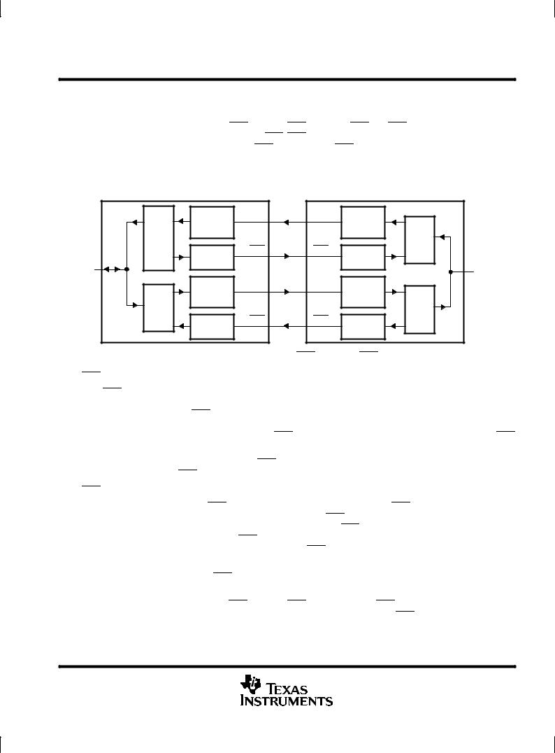
autoflow control (see Figure 1)
Autoflow control is comprised of auto-CTS and auto-RTS. With auto-CTS, the CTS input must be active before the transmitter FIFO can emit data. With auto-RTS, RTS becomes active when the receiver needs more data and notifies the sending serial device. When RTS is connected to CTS, data transmission does not occur unless the receiver FIFO has space for the data; thus, overrun errors are eliminated using ACE1 and ACE2 from a TLC16C550C with the autoflow control enabled. If not, overrun errors occur when the transmit data rate exceeds the receiver FIFO read latency.
ACE1 |
|
|
ACE2 |
|
Serial to |
SIN |
SOUT |
Parallel |
|
Parallel |
|
|
to Serial |
|
RCV |
|
|
XMT |
|
FIFO |
RTS |
CTS |
FIFO |
|
Flow |
Flow |
|||
|
|
|||
Control |
|
|
Control |
|
D7 ± D0 |
|
|
D7 ± D0 |
|
|
|
|
||
Parallel |
SOUT |
SIN |
Serial to |
|
to Serial |
|
|
Parallel |
|
XMT |
|
|
RCV |
|
FIFO |
CTS |
RTS |
FIFO |
|
Flow |
Flow |
|||
|
|
|||
Control |
|
|
Control |
Figure 1. Autoflow Control (Auto-RTS and Auto-CTS) Example
auto-RTS (see Figure 1)
Auto-RTS data flow control originates in the receiver timing and control block (see functional block diagram) and is linked to the programmed receiver FIFO trigger level. When the receiver FIFO level reaches a trigger level of 1, 4, or 8 (see Figure 3), RTS is deasserted. With trigger levels of 1, 4, and 8, the sending ACE may send an additional byte after the trigger level is reached (assuming the sending ACE has another byte to send) because it may not recognize the deassertion of RTS until after it has begun sending the additional byte. RTS is automatically reasserted once the RCV FIFO is emptied by reading the receiver buffer register.
When the trigger level is 14 (see Figure 4), RTS is deasserted after the first data bit of the 16th character is present on the SIN line. RTS is reasserted when the RCV FIFO has at least one available byte space.
auto-CTS (see Figure 1)
The transmitter circuitry checks CTS before sending the next data byte. When CTS is active, it sends the next byte. To stop the transmitter from sending the following byte, CTS must be released before the middle of the last stop bit that is currently being sent (see Figure 2). The auto-CTS function reduces interrupts to the host system. When flow control is enabled, CTS level changes do not trigger host interrupts because the device automatically controls its own transmitter. Without auto-CTS, the transmitter sends any data present in the transmit FIFO and a receiver overrun error may result.
enabling autoflow control and auto-CTS
Autoflow control is enabled by setting modem control register bits 5 (autoflow enable or AFE) and 1 (RTS) to a 1. Autoflow incorporates both auto-RTS and auto-CTS. When only auto-CTS is desired, bit 1 in the modem control register should be cleared (this assumes that a control signal is driving CTS).
POST OFFICE BOX 655303 •DALLAS, TEXAS 75265 |
3 |
TL16C550C, TL16C550CI
ASYNCHRONOUS COMMUNICATIONS ELEMENT
WITH AUTOFLOW CONTROL
SLLS177E ± MARCH 1994 ± REVISED APRIL1998
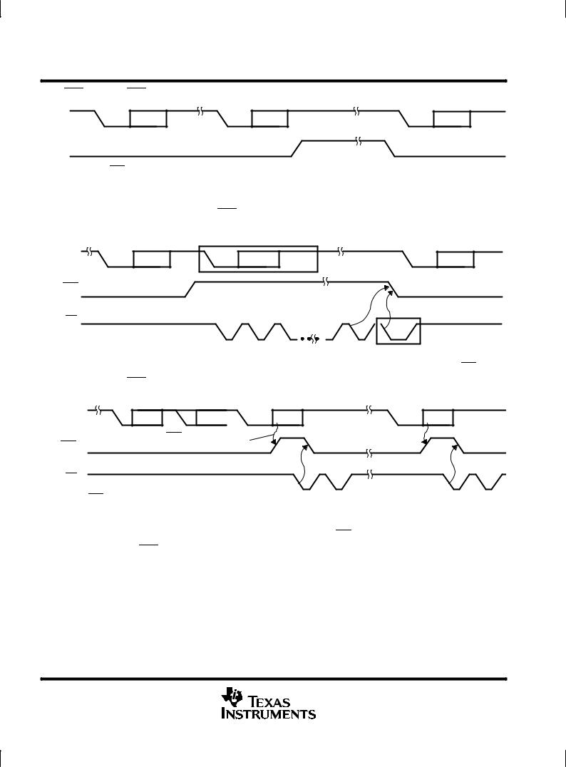
auto-CTS and auto-RTS functional timing
SOUT |
Start Bits 0 ± 7 Stop |
|
Start Bits 0 ± 7 Stop |
|
|
|
Start Bits 0 ± 7 Stop |
||
|
|
|
|
||||||
|
|
|
|
|
|
|
|
|
|
|
|
|
|
|
|
|
|
|
|
CTS
NOTES: A. When CTS is low, the transmitter keeps sending serial data out.
B.If CTS goes high before the middle of the last stop bit of the current byte, the transmitter finishes sending the current byte but it does not send the next byte.
C.When CTS goes from high to low, the transmitter begins sending data again.
Figure 2. CTS Functional Timing Waveforms
The receiver FIFO trigger level can be set to 1, 4, 8, or 14 bytes. These are described in Figures 3 and 4.
SIN |
Start Byte N Stop |
Start |
Byte N+1 Stop |
|
Start |
Byte |
Stop |
RTS |
|
|
|
|
|
|
|
RD |
|
|
|
|
|
|
|
(RD RBR) |
|
1 |
2 |
N |
N+1 |
|
|
|
|
|
|
NOTES: A. N = RCV FIFO trigger level (1, 4, or 8 bytes)
B. The two blocks in dashed lines cover the case where an additional byte is sent as described in the preceding auto-RTS section.
Figure 3. RTS Functional Timing Waveforms, RCV FIFO Trigger Level = 1,4, or 8 Bytes
SIN |
Byte 14 |
Byte 15 |
Start Byte 16 Stop |
Start Byte 18 Stop |
|
|
RTS Released After the |
|
|
RTS |
|
First Data Bit of Byte 16 |
|
|
RD (RD RBR)
NOTES: A. RTS is deasserted when the receiver receives the first data bit of the sixteenth byte. The receive FIFO is full after finishing the sixteenth byte.
B.RTS is asserted again when there is at least one byte of space available and no incoming byte is in processing or there is more than one byte of space available.
C.When the receive FIFO is full, the first receive buffer register read reasserts RTS.
Figure 4. RTS Functional Timing Waveforms, RCV FIFO Trigger Level = 14 Bytes
4 |
POST OFFICE BOX 655303 •DALLAS, TEXAS 75265 |

TL16C550C, TL16C550CI
ASYNCHRONOUS COMMUNICATIONS ELEMENT
WITH AUTOFLOW CONTROL
SLLS177E ± MARCH 1994 ± REVISED APRIL1998
functional block diagram
D(7 ± 0)
A0
A1
A2
CS0
CS1
CS2
ADS
MR
RD1
RD2
WR1
WR2
DDIS TXRDY XIN XOUT RXRDY
VCC
VSS
|
|
|
S |
|
|
|
|
|
|
|
|
|
|
|
e |
|
|
|
|
|
|
|
|
|
Internal |
8 |
l |
|
|
Receiver |
|
|
|
|
|
|
e |
|
|
FIFO |
|
|
|
|
|
||
|
|
8 |
|
|
|
|
|
|
|||
|
Data Bus |
|
|
|
|
|
|
|
|||
|
|
c |
|
|
|
|
|
|
|
||
|
|
|
|
|
|
|
|
|
|
|
|
|
|
|
t |
|
|
|
|
|
|
|
|
|
|
|
|
|
|
|
|
|
Receiver |
10 |
|
8 ±1 |
Data |
|
|
Receiver |
|
|
|
|
Shift |
SIN |
|
|
|
|
|
|
|
|
|||||
|
Bus |
|
|
Buffer |
|
|
|
|
Register |
|
|
|
Buffer |
|
|
Register |
|
|
|
|
|
|
|
|
|
|
|
Line |
|
|
|
|
Receiver |
9 |
RCLK |
|
|
|
|
|
|
|
|
Timing and |
|
|
|
|
|
|
|
Control |
|
|
|
|
|
|
|
|
|
|
|
|
|
|
|
Control |
32 |
|
|
|
|
|
|
Register |
|
|
|
|
|
||
|
|
|
|
|
|
|
|
|
RTS |
||
|
|
|
|
|
|
|
|
|
|
|
|
28 |
|
|
|
|
|
|
|
|
|
|
|
27 |
|
|
|
Divisor |
|
|
|
|
|
|
|
|
|
|
|
|
|
|
|
|
|
|
|
26 |
|
|
|
Latch (LS) |
|
Baud |
|
|
|
15 |
|
|
|
|
|
Divisor |
|
Generator |
|
|
|
BAUDOUT |
|
|
|
|
|
|
|
|
|
|
|
||
12 |
|
|
|
|
|
|
|
|
|
|
|
|
|
|
Latch (MS) |
|
|
|
|
|
|
|
|
13 |
|
|
|
|
|
|
|
|
|
Autoflow |
|
14 |
|
|
|
|
|
|
|
|
Transmitter |
Control |
|
|
|
|
Line |
|
|
|
|
(AFE) |
|
||
|
|
|
|
|
|
|
|
Timing and |
|
||
25 |
|
|
|
Status |
|
|
|
|
|
|
|
|
|
|
|
|
|
|
Control |
|
|
||
|
|
|
Register |
|
|
|
|
|
|
||
35 |
Select |
|
|
|
|
|
|
|
|
|
|
|
|
|
|
Transmitter |
|
|
|
|
|
||
21 |
and |
|
|
|
|
S |
|
|
|
|
|
Control |
|
|
|
|
FIFO |
e |
|
|
|
|
|
|
|
|
|
|
|
|
|
|
|||
22 |
Logic |
|
|
|
|
|
l |
|
|
|
|
18 |
|
|
|
Transmitter |
|
8 |
e |
8 |
Transmitter |
11 |
|
|
|
|
Holding |
|
|
c |
|
Shift |
|
SOUT |
|
19 |
|
|
|
Register |
|
|
t |
|
Register |
|
|
23 |
|
|
|
|
|
|
|
|
|
|
|
24 |
|
|
|
Modem |
|
8 |
|
|
|
|
|
|
|
|
Control |
|
|
|
|
|
|
||
|
|
|
|
|
|
|
|
|
36 |
|
|
16 |
|
|
|
Register |
|
|
|
|
|
CTS |
|
|
|
|
|
|
|
|
|
|
|
33 |
|
17 |
|
|
|
|
|
|
|
|
Modem |
DTR |
|
|
|
|
|
Modem |
|
8 |
|
|
37 |
||
29 |
|
|
|
|
|
|
DSR |
||||
|
|
|
|
|
|
Control |
|||||
|
|
|
|
Status |
|
|
|
|
38 |
||
|
|
|
|
Register |
|
|
|
|
Logic |
DCD |
|
|
|
|
|
|
|
|
|
|
|
39 |
|
|
|
|
|
|
|
|
|
|
|
RI |
|
40 |
|
|
|
|
|
|
|
|
|
34 |
OUT1 |
|
|
|
|
|
|
|
|
|
31 |
OUT2 |
|
20 |
Power |
|
|
Interrupt |
8 |
Interrupt |
|
|
|
||
Supply |
|
|
|
|
|
30 |
INTRPT |
||||
|
|
|
Enable |
Control |
|
|
|
||||
|
|
|
|
Register |
|
Logic |
|
|
|
|
|
|
|
|
|
Interrupt |
8 |
|
|
|
|
|
|
|
|
|
|
Identification |
|
|
|
|
|
|
|
|
|
|
|
|
|
|
|
|
|
|
|
|
|
|
|
Register |
|
|
|
|
|
|
|
|
|
|
|
FIFO |
|
|
|
|
|
|
|
|
|
|
|
Control |
|
|
|
|
|
|
|
|
|
|
|
Register |
|
|
|
|
|
|
|
NOTE A: Terminal numbers shown are for the N package.
POST OFFICE BOX 655303 •DALLAS, TEXAS 75265 |
5 |

TL16C550C, TL16C550CI
ASYNCHRONOUS COMMUNICATIONS ELEMENT
WITH AUTOFLOW CONTROL
SLLS177E ± MARCH 1994 ± REVISED APRIL1998
|
|
|
|
|
|
|
|
|
|
|
|
|
Terminal Functions |
|||||||||||||||
|
|
|
|
|
|
|
|
|
|
|
|
|
|
|
|
|
|
|
|
|
|
|
|
|
|
|
||
|
|
|
|
|
TERMINAL |
|
|
|
|
|
|
|
|
|
|
|
|
|
|
|
|
|
|
|
|
|
||
|
NAME |
NO. |
NO. |
NO. |
I/O |
|
|
|
|
|
|
|
|
|
|
|
DESCRIPTION |
|||||||||||
|
N |
FN |
PT |
|
|
|
|
|
|
|
|
|
|
|
|
|
|
|
|
|
|
|
|
|||||
|
|
|
|
|
|
|
|
|
|
|
|
|
|
|
|
|
|
|
|
|
|
|
|
|
|
|||
|
|
|
|
|
|
|
|
|
|
|
|
|
|
|
|
|
|
|
|
|
|
|
|
|
|
|
|
|
|
A0 |
28 |
31 |
28 |
I |
Register select. A0 ± A2 are used during read and write operations to select the ACE register to read |
||||||||||||||||||||||
|
A1 |
27 |
30 |
27 |
|
from or write to. Refer to Table 1 for register addresses and refer to ADS description. |
||||||||||||||||||||||
|
A2 |
26 |
29 |
26 |
|
|
|
|
|
|
|
|
|
|
|
|
|
|
|
|
|
|
|
|
||||
|
|
|
|
|
|
|
|
|
|
|
|
|
|
|
|
|
|
|
|
|
|
|
|
|
|
|
|
|
|
|
|
|
|
|
25 |
28 |
24 |
I |
Address strobe. When |
|
|
is active (low), A0, A1, and A2 and CS0, CS1, and |
|
drive the internal |
|||||||||||||
|
ADS |
|
|
|
ADS |
CS2 |
||||||||||||||||||||||
|
|
|
|
|
|
|
|
|
|
select logic directly; when ADS is high, the register select and chip select signals are held at the logic |
||||||||||||||||||
|
|
|
|
|
|
|
|
|
|
levels they were in when the low-to-high transition of ADS occurred. |
||||||||||||||||||
|
|
|
|
|
|
|
|
|
|
|
|
|
|
|
|
|
|
|
|
|
|
|
|
|||||
|
|
|
|
|
|
15 |
17 |
12 |
O |
Baud out. |
|
|
|
|
|
|
is a 16 × clock signal for the transmitter section of the ACE. The clock rate is |
|||||||||||
|
BAUDOUT |
BAUDOUT |
||||||||||||||||||||||||||
|
|
|
|
|
|
|
|
|
|
established by the reference oscillator frequency divided by a divisor specified by the baud generator |
||||||||||||||||||
|
|
|
|
|
|
|
|
|
|
divisor latches. BAUDOUT may also be used for the receiver section by tying this output to RCLK. |
||||||||||||||||||
|
|
|
|
|
|
|
|
|
|
|
|
|
|
|
|
|
|
|
|
|||||||||
|
CS0 |
12 |
14 |
9 |
I |
Chip select. When CS0 and CS1 are high and |
|
|
is low, these three inputs select the ACE. When any |
|||||||||||||||||||
|
CS2 |
|||||||||||||||||||||||||||
|
CS1 |
13 |
15 |
10 |
|
of these inputs are inactive, the ACE remains inactive (refer to ADS description). |
||||||||||||||||||||||
|
CS2 |
14 |
16 |
11 |
|
|
|
|
|
|
|
|
|
|
|
|
|
|
|
|
|
|
|
|
||||
|
|
|
|
|
|
|
|
|
|
|
|
|
|
|
|
|
|
|
||||||||||
|
|
|
|
|
|
36 |
40 |
38 |
I |
Clear to send. |
|
|
|
is a modem status signal. Its condition can be checked by reading bit 4 (CTS) of |
||||||||||||||
|
CTS |
|
|
|
CTS |
|
||||||||||||||||||||||
|
|
|
|
|
|
|
|
|
|
the modem status register. Bit 0 (D CTS) of the modem status register indicates that CTS has changed |
||||||||||||||||||
|
|
|
|
|
|
|
|
|
|
states since the last read from the modem status register. If the modem status interrupt is enabled when |
||||||||||||||||||
|
|
|
|
|
|
|
|
|
|
CTS changes levels and the auto-CTS mode is not enabled, an interrupt is generated. |
CTS |
is also used |
||||||||||||||||
|
|
|
|
|
|
|
|
|
|
in the auto-CTS mode to control the transmitter. |
||||||||||||||||||
|
|
|
|
|
|
|
|
|
|
|
|
|
|
|
||||||||||||||
|
D0 |
1 |
2 |
43 |
I/O |
Data bus. Eight data lines with 3-state outputs provide a bidirectional path for data, control, and status |
||||||||||||||||||||||
|
D1 |
2 |
3 |
44 |
|
information between the ACE and the CPU. |
||||||||||||||||||||||
|
D2 |
3 |
4 |
45 |
|
|
|
|
|
|
|
|
|
|
|
|
|
|
|
|
|
|
|
|
||||
|
D3 |
4 |
5 |
46 |
|
|
|
|
|
|
|
|
|
|
|
|
|
|
|
|
|
|
|
|
||||
|
D4 |
5 |
6 |
47 |
|
|
|
|
|
|
|
|
|
|
|
|
|
|
|
|
|
|
|
|
||||
|
D5 |
6 |
7 |
2 |
|
|
|
|
|
|
|
|
|
|
|
|
|
|
|
|
|
|
|
|
||||
|
D6 |
7 |
8 |
3 |
|
|
|
|
|
|
|
|
|
|
|
|
|
|
|
|
|
|
|
|
||||
|
D7 |
8 |
9 |
4 |
|
|
|
|
|
|
|
|
|
|
|
|
|
|
|
|
|
|
|
|
||||
|
|
|
|
|
|
|
|
|
|
|
|
|
|
|||||||||||||||
|
|
|
|
|
|
38 |
42 |
40 |
I |
Data carrier detect. |
|
|
|
|
is a modem status signal. Its condition can be checked by reading bit 7 (DCD) |
|||||||||||||
|
DCD |
|
DCD |
|||||||||||||||||||||||||
|
|
|
|
|
|
|
|
|
|
of the modem status register. Bit 3 (D DCD) of the modem status register indicates that DCD has |
||||||||||||||||||
|
|
|
|
|
|
|
|
|
|
changed states since the last read from the modem status register. If the modem status interrupt is |
||||||||||||||||||
|
|
|
|
|
|
|
|
|
|
enabled when DCD changes levels, an interrupt is generated. |
||||||||||||||||||
|
|
|
|
|
|
|
|
|
|
|
|
|||||||||||||||||
|
DDIS |
23 |
26 |
22 |
O |
Driver disable. DDIS is active (high) when the CPU is not reading data. When active, DDIS can disable |
||||||||||||||||||||||
|
|
|
|
|
|
|
|
|
|
an external transceiver. |
||||||||||||||||||
|
|
|
|
|
|
|
|
|
|
|
||||||||||||||||||
|
|
|
|
|
|
37 |
41 |
39 |
I |
Data set ready. |
|
|
|
is a modem status signal. Its condition can be checked by reading bit 5 (DSR) of |
||||||||||||||
|
DSR |
|
DSR |
|||||||||||||||||||||||||
|
|
|
|
|
|
|
|
|
|
the modem status register. Bit 1 (D DSR) of the modem status register indicates DSR has changed |
||||||||||||||||||
|
|
|
|
|
|
|
|
|
|
levels since the last read from the modem status register. If the modem status interrupt is enabled when |
||||||||||||||||||
|
|
|
|
|
|
|
|
|
|
DSR changes levels, an interrupt is generated. |
||||||||||||||||||
|
|
|
|
|
|
|
|
|
||||||||||||||||||||
|
|
|
|
|
|
33 |
37 |
33 |
O |
Data terminal ready. When active (low), |
|
|
informs a modem or data set that the ACE is ready to |
|||||||||||||||
|
DTR |
|
DTR |
|||||||||||||||||||||||||
|
|
|
|
|
|
|
|
|
|
establish communication. DTR is placed in the active level by setting the DTR bit of the modem control |
||||||||||||||||||
|
|
|
|
|
|
|
|
|
|
register. DTR is placed in the inactive level either as a result of a master reset, during loop mode |
||||||||||||||||||
|
|
|
|
|
|
|
|
|
|
operation, or clearing the DTR bit. |
||||||||||||||||||
|
|
|
|
|
|
|
||||||||||||||||||||||
|
INTRPT |
30 |
33 |
30 |
O |
Interrupt. When active (high), INTRPT informs the CPU that the ACE has an interrupt to be serviced. |
||||||||||||||||||||||
|
|
|
|
|
|
|
|
|
|
Four conditions that cause an interrupt to be issued are: a receiver error, received data that is available |
||||||||||||||||||
|
|
|
|
|
|
|
|
|
|
or timed out (FIFO mode only), an empty transmitter holding register, or an enabled modem status |
||||||||||||||||||
|
|
|
|
|
|
|
|
|
|
interrupt. INTRPT is reset (deactivated) either when the interrupt is serviced or as a result of a master |
||||||||||||||||||
|
|
|
|
|
|
|
|
|
|
reset. |
||||||||||||||||||
|
|
|
|
|
|
|
||||||||||||||||||||||
|
MR |
35 |
39 |
35 |
I |
Master reset. When active (high), MR clears most ACE registers and sets the levels of various output |
||||||||||||||||||||||
|
|
|
|
|
|
|
|
|
|
signals (refer to Table 2). |
||||||||||||||||||
|
|
|
|
|
|
|
|
|
|
|
|
|
|
|
|
|
|
|
|
|
|
|
|
|
|
|
|
|
6 |
POST OFFICE BOX 655303 •DALLAS, TEXAS 75265 |

|
|
|
|
|
|
|
|
|
|
|
|
|
|
|
|
|
|
|
|
|
|
TL16C550C, TL16C550CI |
||||||
|
|
|
|
|
|
|
|
|
|
|
|
|
|
|
ASYNCHRONOUS COMMUNICATIONS ELEMENT |
|||||||||||||
|
|
|
|
|
|
|
|
|
|
|
|
|
|
|
|
|
|
|
|
|
WITH AUTOFLOW CONTROL |
|||||||
|
|
|
|
|
|
|
|
|
|
|
|
|
|
|
|
|
|
|
|
|
SLLS177E ± MARCH 1994 ± REVISED APRIL1998 |
|||||||
|
|
|
|
|
|
|
|
|
|
|
|
|
|
|
|
|
|
|
|
|
|
|
|
|
|
|
|
|
|
|
|
|
|
|
|
|
|
|
|
|
|
Terminal Functions (Continued) |
|||||||||||||||
|
|
|
|
|
|
|
|
|
|
|
|
|
|
|
|
|
|
|
|
|
|
|
|
|
|
|
|
|
|
|
|
|
|
|
|
|
|
TERMINAL |
|
|
|
|
|
|
|
|
|
|
|
|
|
|
|
|
|
|
|
|
NAME |
NO. |
NO. |
NO. |
I/O |
|
|
|
|
|
|
|
|
DESCRIPTION |
|
|||||||||||||
|
N |
FN |
PT |
|
|
|
|
|
|
|
|
|
|
|
|
|
|
|
|
|
||||||||
|
|
|
|
|
|
|
|
|
|
|
|
|
|
|
|
|
|
|
|
|
|
|
|
|
|
|||
|
|
|
|
|
|
|
|
|
|
|
|
|
|
|
|
|
|
|
|
|
|
|
|
|
|
|
|
|
|
|
|
|
|
|
|
|
|
34 |
38 |
34 |
O |
Outputs 1 and 2. These are user-designated output terminals that are set to the active (low) level by |
|
||||||||||||||
|
OUT1 |
|
|
|
|
|||||||||||||||||||||||
|
OUT2 |
31 |
35 |
31 |
|
setting respective modem control register (MCR) bits (OUT1 and OUT2). |
OUT1 |
and OUT2 are set to |
|
|||||||||||||||||||
|
|
|
|
|
|
|
|
|
|
|
|
|
inactive the (high) level as a result of master reset, during loop mode operations, or by clearing bit 2 |
|
||||||||||||||
|
|
|
|
|
|
|
|
|
|
|
|
|
(OUT1) or bit 3 (OUT2) of the MCR. |
|
||||||||||||||
|
|
|
|
|
|
|
|
|
|
|
|
|
|
|
|
|
|
|
|
|
|
|
|
|
|
|||
|
RCLK |
9 |
10 |
5 |
I |
Receiver clock. RCLK is the 16 × baud rate clock for the receiver section of the ACE. |
|
|||||||||||||||||||||
|
|
|
|
|
|
|
|
|
|
|
|
|
|
|
|
|
|
|
|
|
|
|
|
|
||||
|
|
|
|
|
|
|
|
|
21 |
24 |
19 |
I |
Read inputs. When either |
|
|
or RD2 is active (low or high respectively) while the ACE is selected, |
|
|||||||||||
|
RD1 |
|
|
|
|
RD1 |
|
|||||||||||||||||||||
|
RD2 |
22 |
25 |
20 |
|
the CPU is allowed to read status information or data from a selected ACE register. Only one of these |
|
|||||||||||||||||||||
|
|
|
|
|
|
|
|
|
|
|
|
|
inputs is required for the transfer of data during a read operation; the other input should be tied to its |
|
||||||||||||||
|
|
|
|
|
|
|
|
|
|
|
|
|
inactive level (i.e., RD2 tied low or RD1 tied high). |
|
||||||||||||||
|
|
|
|
|
|
|
|
|
|
|
|
|
|
|
|
|
|
|
|
|
|
|||||||
|
|
|
|
|
|
|
|
|
39 |
43 |
41 |
I |
Ring indicator. |
|
is a modem status signal. Its condition can be checked by reading bit 6 (RI) of the |
|
||||||||||||
|
RI |
|
|
|
|
|
RI |
|
||||||||||||||||||||
|
|
|
|
|
|
|
|
|
|
|
|
|
modem status register. Bit 2 (TERI) of the modem status register indicates that RI has transitioned from |
|
||||||||||||||
|
|
|
|
|
|
|
|
|
|
|
|
|
a low to a high level since the last read from the modem status register. If the modem status interrupt |
|
||||||||||||||
|
|
|
|
|
|
|
|
|
|
|
|
|
is enabled when this transition occurs, an interrupt is generated. |
|
||||||||||||||
|
|
|
|
|
|
|
|
|
|
|
|
|
|
|
|
|
|
|
||||||||||
|
|
|
|
|
|
|
|
|
32 |
36 |
32 |
O |
Request to send. When active, |
|
|
informs the modem or data set that the ACE is ready to receive |
|
|||||||||||
|
RTS |
|
|
|
|
RTS |
|
|||||||||||||||||||||
|
|
|
|
|
|
|
|
|
|
|
|
|
data. RTS is set to the active level by setting the RTS modem control register bit and is set to the inactive |
|
||||||||||||||
|
|
|
|
|
|
|
|
|
|
|
|
|
(high) level either as a result of a master reset or during loop mode operations or by clearing bit 1 (RTS) |
|
||||||||||||||
|
|
|
|
|
|
|
|
|
|
|
|
|
of the MCR. In the auto-RTS mode, RTS is set to the inactive level by the receiver threshold control logic. |
|
||||||||||||||
|
|
|
|
|
|
|
|
|
|
|
|
|
|
|
|
|||||||||||||
|
|
|
|
|
|
|
|
|
29 |
32 |
29 |
O |
Receiver ready. Receiver direct memory access (DMA) signalling is available with |
|
When |
|
||||||||||||
|
RXRDY |
|
RXRDY. |
|
||||||||||||||||||||||||
|
|
|
|
|
|
|
|
|
|
|
|
|
operating in the FIFO mode, one of two types of DMA signalling can be selected using the FIFO control |
|
||||||||||||||
|
|
|
|
|
|
|
|
|
|
|
|
|
register bit 3 (FCR3). When operating in the TL16C450 mode, only DMA mode 0 is allowed. Mode 0 |
|
||||||||||||||
|
|
|
|
|
|
|
|
|
|
|
|
|
supports single-transfer DMA in which a transfer is made between CPU bus cycles. Mode 1 supports |
|
||||||||||||||
|
|
|
|
|
|
|
|
|
|
|
|
|
multitransfer DMA in which multiple transfers are made continuously until the receiver FIFO has been |
|
||||||||||||||
|
|
|
|
|
|
|
|
|
|
|
|
|
emptied. In DMA mode 0 (FCR0 = 0 or FCR0 = 1, FCR3 = 0), when there is at least one character in |
|
||||||||||||||
|
|
|
|
|
|
|
|
|
|
|
|
|
the receiver FIFO or receiver holding register, RXRDY is active (low). When RXRDY has been active |
|
||||||||||||||
|
|
|
|
|
|
|
|
|
|
|
|
|
but there are no characters in the FIFO or holding register, RXRDY goes inactive (high). In DMA mode 1 |
|
||||||||||||||
|
|
|
|
|
|
|
|
|
|
|
|
|
(FCR0 = 1, FCR3 = 1), when the trigger level or the time-out has been reached, RXRDY goes active |
|
||||||||||||||
|
|
|
|
|
|
|
|
|
|
|
|
|
(low); when it has been active but there are no more characters in the FIFO or holding register, it goes |
|
||||||||||||||
|
|
|
|
|
|
|
|
|
|
|
|
|
inactive (high). |
|
||||||||||||||
|
|
|
|
|
|
|
|
|
|
|
|
|
|
|||||||||||||||
|
SIN |
10 |
11 |
7 |
I |
Serial data input. SIN is serial data input from a connected communications device |
|
|||||||||||||||||||||
|
|
|
|
|
|
|
|
|
|
|
|
|
|
|||||||||||||||
|
SOUT |
11 |
13 |
8 |
O |
Serial data output. SOUT is composite serial data output to a connected communication device. SOUT |
|
|||||||||||||||||||||
|
|
|
|
|
|
|
|
|
|
|
|
|
is set to the marking (high) level as a result of master reset. |
|
||||||||||||||
|
|
|
|
|
|
|
|
|
|
|
|
|
||||||||||||||||
|
|
|
|
|
|
|
|
|
24 |
27 |
23 |
O |
Transmitter ready. Transmitter DMA signalling is available with |
|
When operating in the FIFO |
|
||||||||||||
|
TXRDY |
|
TXRDY. |
|
||||||||||||||||||||||||
|
|
|
|
|
|
|
|
|
|
|
|
|
mode, one of two types of DMA signalling can be selected using FCR3. When operating in the |
|
||||||||||||||
|
|
|
|
|
|
|
|
|
|
|
|
|
TL16C450 mode, only DMA mode 0 is allowed. Mode 0 supports single-transfer DMA in which a transfer |
|
||||||||||||||
|
|
|
|
|
|
|
|
|
|
|
|
|
is made between CPU bus cycles. Mode 1 supports multitransfer DMA in which multiple transfers are |
|
||||||||||||||
|
|
|
|
|
|
|
|
|
|
|
|
|
made continuously until the transmit FIFO has been filled. |
|
||||||||||||||
|
|
|
|
|
|
|
|
|
|
|
||||||||||||||||||
|
VCC |
40 |
44 |
42 |
|
5-V supply voltage |
|
|||||||||||||||||||||
|
VSS |
20 |
22 |
18 |
|
Supply common |
|
|||||||||||||||||||||
|
|
|
|
|
|
|
|
|
18 |
20 |
16 |
I |
Write inputs. When either |
|
|
|
or WR2 is active (low or high respectively) and while the ACE is |
|
||||||||||
|
WR1 |
|
WR1 |
|
||||||||||||||||||||||||
|
WR2 |
19 |
21 |
17 |
|
selected, the CPU is allowed to write control words or data into a selected ACE register. Only one of |
|
|||||||||||||||||||||
|
|
|
|
|
|
|
|
|
|
|
|
|
these inputs is required to transfer data during a write operation; the other input should be tied to its |
|
||||||||||||||
|
|
|
|
|
|
|
|
|
|
|
|
|
inactive level (i.e., WR2 tied low or WR1 tied high). |
|
||||||||||||||
|
|
|
|
|
|
|
|
|||||||||||||||||||||
|
XIN |
16 |
18 |
14 |
I/O |
External clock. XIN and XOUT connect the ACE to the main timing reference (clock or crystal). |
|
|||||||||||||||||||||
|
XOUT |
17 |
19 |
15 |
|
|
|
|
|
|
|
|
|
|
|
|
|
|
|
|
|
|||||||
|
|
|
|
|
|
|
|
|
|
|
|
|
|
|
|
|
|
|
|
|
|
|
|
|
|
|
|
|
POST OFFICE BOX 655303 •DALLAS, TEXAS 75265 |
7 |

TL16C550C, TL16C550CI
ASYNCHRONOUS COMMUNICATIONS ELEMENT
WITH AUTOFLOW CONTROL
SLLS177E ± MARCH 1994 ± REVISED APRIL1998
absolute maximum ratings over operating free-air temperature range (unless otherwise noted)²
Supply voltage range, VCC (see Note 1) . . . . . . . . . . . . . . . . . . . . . . . . . . . . . . . . . . . . . . . . . . . . |
. . ±0.5 V to 7 V |
Input voltage range at any input, VI . . . . . . . . . . . . . . . . . . . . . . . . . . . . . . . . . . . . . . . . . . . . . . . . . . |
. ±0.5 V to 7 V |
Output voltage range, VO . . . . . . . . . . . . . . . . . . . . . . . . . . . . . . . . . . . . . . . . . . . . . . . . . . . . . . . . . . |
. ±0.5 V to 7 V |
Operating free-air temperature range, TA, TL16C550C . . . . . . . . . . . . . . . . . . . . . . . . . . . . . . . . . |
. . 0°C to 70°C |
TL16C550CI . . . . . . . . . . . . . . . . . . . . . . . . . . . . . . . . |
±40°C to 85°C |
Storage temperature range, Tstg . . . . . . . . . . . . . . . . . . . . . . . . . . . . . . . . . . . . . . . . . . . . . . . . . . . |
±65°C to 150°C |
Case temperature for 10 seconds, TC: FN package . . . . . . . . . . . . . . . . . . . . . . . . . . . . . . . . . . . |
. . . . . . . 260°C |
Lead temperature 1,6 mm (1/16 inch) from case for 10 seconds: N or PT package . . . . . . . . |
. . . . . . . 260°C |
²Stresses beyond those listed under ªabsolute maximum ratingsº may cause permanent damage to the device. These are stress ratings only, and functional operation of the device at these or any other conditions beyond those indicated under ªrecommended operating conditionsº is not implied. Exposure to absolute-maximum-rated conditions for extended periods may affect device reliability.
NOTE 1: All voltage values are with respect to VSS.
recommended operating conditions low voltage (3.3 V nominal)
|
MIN |
NOM |
MAX |
UNIT |
|
|
|
|
|
Supply voltage, VCC |
3 |
3.3 |
3.6 |
V |
Input voltage, VI |
0 |
|
VCC |
V |
High-level input voltage, VIH (see Note 2) |
0.7 VCC |
|
|
V |
Low-level input voltage, VIL (see Note 2) |
|
|
0.3 VCC |
V |
Output voltage, VO (see Note 3) |
0 |
|
VCC |
V |
High-level output current, IOH (all outputs) |
|
|
1.8 |
mA |
Low-level output current, IOL (all outputs) |
|
|
3.2 |
mA |
Input capacitance |
|
|
1 |
pF |
|
|
|
|
|
Operating free-air temperature, TA |
0 |
25 |
70 |
°C |
Junction temperature range, TJ (see Note 4) |
0 |
25 |
115 |
°C |
Oscillator/clock speed |
|
|
14 |
MHz |
|
|
|
|
|
NOTES: 2. Meets TTL levels, VIHmin = 2 V and VILmax = 0.8 V on nonhysteresis inputs
3.Applies for external output buffers
4.These junction temperatures reflect simulated conditions. Absolute maximum junction temperature is 150°C. The customer is responsible for verifying junction temperature.
standard voltage (5 V nominal)
|
MIN |
NOM |
MAX |
UNIT |
|
|
|
|
|
Supply voltage, VCC |
4.75 |
5 |
5.25 |
V |
Input voltage, VI |
0 |
|
VCC |
V |
High-level input voltage, VIH |
0.7 VCC |
|
|
V |
Low-level input voltage, VIL |
|
|
0.2 VCC |
V |
Output voltage, VO (see Note 5) |
0 |
|
VCC |
V |
High-level output current, IOH (all outputs) |
|
|
4 |
mA |
Low-level output current, IOL (all outputs) |
|
|
4 |
mA |
Input capacitance |
|
|
1 |
pF |
|
|
|
|
|
Operating free-air temperature, TA |
0 |
25 |
70 |
°C |
Junction temperature range, TJ (see Note 6) |
0 |
25 |
115 |
°C |
Oscillator/clock speed |
|
|
16 |
MHz |
5.Applies for external output buffers
6.These junction temperatures reflect simulated conditions. Absolute maximum junction temperature is 150°C. The customer is responsible for verifying junction temperature.
8 |
POST OFFICE BOX 655303 •DALLAS, TEXAS 75265 |

TL16C550C, TL16C550CI
ASYNCHRONOUS COMMUNICATIONS ELEMENT
WITH AUTOFLOW CONTROL
SLLS177E ± MARCH 1994 ± REVISED APRIL1998
electrical characteristics over recommended ranges of supply voltage and operating free-air temperature (unless otherwise noted)
low voltage (3.3 V nominal)
|
PARAMETER |
|
|
|
|
TEST CONDITIONS |
MIN TYP² |
MAX |
UNIT |
|||||||
VOH³ |
High-level output voltage |
IOH = ± 1 mA |
|
|
|
2.4 |
|
V |
||||||||
VOL³ |
Low-level output voltage |
IOL = 1.6 mA |
|
|
|
|
0.5 |
V |
||||||||
Il |
Input current |
|
|
VCC = 3.6 V, |
VSS = 0, |
|
10 |
μA |
||||||||
|
|
VI = 0 to 3.6 V, |
All other terminals floating |
|
||||||||||||
|
|
|
|
|
|
|
||||||||||
IOZ |
High-impedance-state output current |
VCC = 3.6 V, |
VSS = 0, |
|
± 20 |
μA |
||||||||||
VO = 0 to 3.6 V, |
|
|
|
|
||||||||||||
|
|
|
|
Chip selected in write mode or chip deselect |
|
|
|
|||||||||
|
|
|
|
|
|
|
|
|
|
|
|
|
|
|
|
|
|
|
|
|
VCC |
= 3.6 V, |
|
TA |
= 25°C, |
|
|
|
|||||
|
|
|
|
|
|
|
|
|
|
|
|
|
|
|||
ICC |
Supply current |
|
|
SIN, |
DSR, DCD, CTS, and RI at 2 V, |
|
8 |
mA |
||||||||
|
|
All other inputs at 0.8 V, |
XTAL1 at 4 MHz, |
|
||||||||||||
|
|
|
|
|
|
|
||||||||||
|
|
|
|
No load on outputs, |
Baud rate = 50 kbit/s |
|
|
|
||||||||
|
|
|
|
|
|
|
|
|
|
|
|
|
|
|
||
Ci(CLK) |
Clock input capacitance |
VCC = 0, |
VSS = 0, |
15 |
20 |
pF |
||||||||||
Co(CLK) |
Clock output capacitance |
20 |
30 |
pF |
||||||||||||
|
|
|
|
f = 1 MHz, |
TA = 25°C, |
|
|
|
||||||||
Ci |
Input capacitance |
|
6 |
10 |
pF |
|||||||||||
|
All other terminals grounded |
|||||||||||||||
Co |
Output capacitance |
|
|
|
|
|
|
|
|
|
|
10 |
20 |
pF |
||
² All typical values are at V |
CC |
= 3.3 V and T = 25°C. |
|
|
|
|
|
|
||||||||
|
|
A |
|
|
|
|
|
|
|
|
|
|
|
|
|
|
³ These parameters apply for all outputs except XOUT.
standard voltage (5 V nominal)
|
PARAMETER |
|
|
|
|
TEST CONDITIONS |
MIN TYP² |
MAX |
UNIT |
|||||||
VOH³ |
High-level output voltage |
IOH = ± 1 mA |
|
|
|
2.4 |
|
V |
||||||||
VOL³ |
Low-level output voltage |
IOL = 1.6 mA |
|
|
|
|
0.4 |
V |
||||||||
Il |
Input current |
|
|
VCC = 5.25 V, |
VSS = 0, |
|
10 |
μA |
||||||||
|
|
VI = 0 to 5.25 V, |
All other terminals floating |
|
||||||||||||
|
|
|
|
|
|
|
||||||||||
IOZ |
High-impedance-state output current |
VCC = 5.25 V, |
VSS = 0, |
|
± 20 |
μA |
||||||||||
VO = 0 to 5.25 V, |
|
|
|
|
||||||||||||
|
|
|
|
Chip selected in write mode or chip deselect |
|
|
|
|||||||||
|
|
|
|
|
|
|
|
|
|
|
|
|
|
|
|
|
|
|
|
|
VCC |
= 5. |
25 V, |
|
|
|
TA = 25°C, |
|
|
|
|||
ICC |
Supply current |
|
|
SIN, |
DSR, |
|
DCD, |
|
CTS, |
and |
RI |
at 2 V, |
|
10 |
mA |
|
|
|
All other inputs at 0.8 V, |
XTAL1 at 4 MHz, |
|
||||||||||||
|
|
|
|
|
|
|
||||||||||
|
|
|
|
No load on outputs, |
Baud rate = 50 kbit/s |
|
|
|
||||||||
|
|
|
|
|
|
|
|
|
|
|
|
|
|
|
||
Ci(CLK) |
Clock input capacitance |
VCC = 0, |
VSS = 0, |
15 |
20 |
pF |
||||||||||
Co(CLK) |
Clock output capacitance |
20 |
30 |
pF |
||||||||||||
|
|
|
|
f = 1 MHz, |
TA = 25°C, |
|
|
|
||||||||
Ci |
Input capacitance |
|
6 |
10 |
pF |
|||||||||||
|
All other terminals grounded |
|||||||||||||||
Co |
Output capacitance |
|
|
|
|
|
|
|
|
|
|
10 |
20 |
pF |
||
² All typical values are at V |
CC |
= 5 V and T = 25°C. |
|
|
|
|
|
|
||||||||
|
|
A |
|
|
|
|
|
|
|
|
|
|
|
|
|
|
³ These parameters apply for all outputs except XOUT.
POST OFFICE BOX 655303 •DALLAS, TEXAS 75265 |
9 |
TL16C550C, TL16C550CI
ASYNCHRONOUS COMMUNICATIONS ELEMENT
WITH AUTOFLOW CONTROL
SLLS177E ± MARCH 1994 ± REVISED APRIL1998
system timing requirements over recommended ranges of supply voltage and operating free-air temperature
|
|
|
|
|
|
|
|
|
|
|
|
|
|
|
|
|
|
|
|
|
|
|
|
|
|
|
|
|
|
|
|
|
|
|
|
|
|
|
|
|
|
ALT. SYMBOL |
FIGURE |
TEST CONDITIONS |
MIN MAX |
UNIT |
|
|
|
|
|
|
|
|
|
|
|
|
|
|
|
|
|
|
|
|
|
|
|
|
|
|
|
|
|
|
|
|
|
|
|
|
|
|
|
|
|
|
|
|
|
|
|
|
|
tcR |
Cycle time, read (tw7 + td8 + td9) |
RC |
|
|
87 |
ns |
|||||||||||||||||||||||||||||||||||||||||
tcW |
Cycle time, write (tw6 + td5 + td6) |
WC |
|
|
87 |
ns |
|||||||||||||||||||||||||||||||||||||||||
tw1 |
Pulse duration, clock high |
tXH |
5 |
f = 16 MHz Max, |
25 |
ns |
|||||||||||||||||||||||||||||||||||||||||
tw2 |
Pulse duration, clock low |
tXL |
VCC = 5 V |
||||||||||||||||||||||||||||||||||||||||||||
|
|
|
|||||||||||||||||||||||||||||||||||||||||||||
tw5 |
Pulse duration, |
|
|
|
|
|
|
low |
tADS |
6, 7 |
|
9 |
ns |
||||||||||||||||||||||||||||||||||
ADS |
|
||||||||||||||||||||||||||||||||||||||||||||||
tw6 |
Pulse duration, |
|
|
|
|
|
|
|
|
|
|
|
|
|
|
|
|
|
|
|
|
|
|
|
|
|
|
|
|
|
|
|
|
|
|
|
|
|
tWR |
6 |
|
40 |
ns |
||||
WR |
|
|
|
|
|
|
|
|
|
|
|
|
|
|
|
|
|
|
|
|
|
|
|
|
|
|
|
|
|
|
|
||||||||||||||||
tw7 |
Pulse duration, |
|
|
|
|
|
|
|
|
|
|
|
|
|
|
|
|
|
|
|
|
|
|
|
|
|
|
|
|
|
|
|
|
|
|
|
|
tRD |
7 |
|
40 |
ns |
|||||
RD |
|
|
|
|
|
|
|
|
|
|
|
|
|
|
|
|
|
|
|
|
|
|
|
|
|
|
|
|
|
|
|
||||||||||||||||
tw8 |
Pulse duration, MR |
tMR |
|
|
1 |
ms |
|||||||||||||||||||||||||||||||||||||||||
tsu1 |
Setup time, address valid before |
|
|
|
|
|
|
|
↑ |
tAS |
|
|
|
|
|||||||||||||||||||||||||||||||||
ADS |
6, 7 |
|
8 |
ns |
|||||||||||||||||||||||||||||||||||||||||||
|
|
|
|
|
|
|
|
|
|
|
|
|
|
|
|
|
|
|
|
|
|
|
|
|
|
|
|
|
|
|
|
|
|
|
|
|
|
|
|
|
|
|
|
||||
tsu2 |
Setup time, CS valid before ADS↑ |
tCS |
|
||||||||||||||||||||||||||||||||||||||||||||
|
|
|
|
||||||||||||||||||||||||||||||||||||||||||||
tsu3 |
Setup time, data valid before |
|
|
|
|
|
|
|
|
|
↓ or WR2↑ |
tDS |
6 |
|
15 |
ns |
|||||||||||||||||||||||||||||||
WR1 |
|
||||||||||||||||||||||||||||||||||||||||||||||
tsu4 |
Setup time, |
|
|
|
|
|
↑ before midpoint of stop bit |
|
17 |
|
10 |
ns |
|||||||||||||||||||||||||||||||||||
CTS |
|
|
|||||||||||||||||||||||||||||||||||||||||||||
th1 |
Hold time, address low after |
|
|
|
|
|
|
|
|
|
|
↑ |
tAH |
|
|
|
|
||||||||||||||||||||||||||||||
ADS |
6, 7 |
|
0 |
ns |
|||||||||||||||||||||||||||||||||||||||||||
|
|
|
|
|
|
|
|
|
|
|
|
|
|
|
|
|
|
|
|
|
|
|
|
|
|
|
|
|
|
|
|
|
|
|
|
|
|
|
|
|
|
|
|
||||
th2 |
Hold time, CS valid after ADS↑ |
tCH |
|
||||||||||||||||||||||||||||||||||||||||||||
|
|
|
|
||||||||||||||||||||||||||||||||||||||||||||
|
|
|
|
|
|
|
|
|
|
|
|
|
|
|
|
|
|
|
|
|
|
|
|
|
|
|
|
|
|
|
|
||||||||||||||||
th3 |
Hold time, CS valid after |
WR1 |
↑ or WR2↓ |
tWCS |
6 |
|
10 |
ns |
|||||||||||||||||||||||||||||||||||||||
|
|
|
|
|
|
|
|
|
|
|
|
|
|
|
|
|
|
|
|
|
|
|
|
|
|
|
|
|
|
|
|
|
|
|
|
|
|
|
|
|
|
|
|
||||
th4 |
Hold time, address valid after WR1↑ or WR2↓ |
tWA |
|
||||||||||||||||||||||||||||||||||||||||||||
|
|
|
|
||||||||||||||||||||||||||||||||||||||||||||
|
|
|
|
|
|
|
|
|
|
|
|
|
|
|
|
|
|
|
|
|
|
|
|
|
|
|
|
||||||||||||||||||||
th5 |
Hold time, data valid after |
WR1 |
↑ or WR2↓ |
tDH |
6 |
|
5 |
ns |
|||||||||||||||||||||||||||||||||||||||
th6 |
Hold time, chip select valid after |
|
|
|
|
|
|
|
|
↑ or RD2↓ |
tRCS |
7 |
|
10 |
ns |
||||||||||||||||||||||||||||||||
RD1 |
|
||||||||||||||||||||||||||||||||||||||||||||||
th7 |
Hold time, address valid after |
|
|
|
|
|
|
|
|
|
↑ or RD2↓ |
tRA |
7 |
|
20 |
ns |
|||||||||||||||||||||||||||||||
RD1 |
|
||||||||||||||||||||||||||||||||||||||||||||||
td4² |
Delay time, CS valid before |
|
|
|
|
|
|
|
|
|
|
|
|
↓ or WR2↑ |
tCSW |
|
|
|
|
||||||||||||||||||||||||||||
WR1 |
6 |
|
7 |
ns |
|||||||||||||||||||||||||||||||||||||||||||
td5² |
|
|
|
|
|
|
|
|
|
|
|
|
|
|
|
|
|
|
|
|
|
|
|
|
|
|
|
|
|
|
|
|
|
|
|
|
|
|
|
|
|
|
|
||||
Delay time, address valid before WR1↓ or WR2↑ |
tAW |
|
|||||||||||||||||||||||||||||||||||||||||||||
|
|
|
|
||||||||||||||||||||||||||||||||||||||||||||
td6² |
Delay time, write cycle, |
|
|
|
|
|
|
|
↑ or WR2↓ to |
|
|
↓ |
tWC |
6 |
|
40 |
ns |
||||||||||||||||||||||||||||||
WR1 |
ADS |
|
|||||||||||||||||||||||||||||||||||||||||||||
td7² |
Delay time, CS valid to |
|
|
|
|
|
|
↓ or RD2↑ |
tCSR |
|
|
|
|
||||||||||||||||||||||||||||||||||
RD1 |
7 |
|
7 |
ns |
|||||||||||||||||||||||||||||||||||||||||||
td8² |
|
|
|
|
|
|
|
|
|
|
|
|
|
|
|
|
|
|
|
|
|
|
|
|
|
|
|
|
|
|
|
|
|
|
|
|
|
|
|
|
|
|
|
||||
Delay time, address valid to RD1↓ or RD2↑ |
tAR |
|
|||||||||||||||||||||||||||||||||||||||||||||
|
|
|
|
||||||||||||||||||||||||||||||||||||||||||||
td9 |
Delay time, read cycle, |
|
|
|
|
|
|
↑ or RD2↓ to |
|
|
↓ |
tRC |
7 |
|
40 |
ns |
|||||||||||||||||||||||||||||||
RD1 |
ADS |
|
|||||||||||||||||||||||||||||||||||||||||||||
td10 |
Delay time, |
|
|
|
|
|
↓ or RD2↑ to data valid |
tRVD |
7 |
CL = 75 pF |
45 |
ns |
|||||||||||||||||||||||||||||||||||
RD1 |
|
||||||||||||||||||||||||||||||||||||||||||||||
td11 |
Delay time, |
|
|
|
|
|
|
↑ or RD2↓ to floating data |
tHZ |
7 |
CL = 75 pF |
20 |
ns |
||||||||||||||||||||||||||||||||||
RD1 |
|||||||||||||||||||||||||||||||||||||||||||||||
² Only applies when ADS is low
system switching characteristics over recommended ranges of supply voltage and operating free-air temperature (see Note 7)
PARAMETER |
ALT. SYMBOL |
FIGURE |
TEST CONDITIONS |
MIN |
MAX |
UNIT |
||
|
|
|
|
|
|
|
||
tdis(R) Disable time, |
|
↓↑ or RD2↑↓ to DDIS↑↓ |
tRDD |
7 |
CL = 75 pF |
20 |
|
ns |
RD1 |
|
|||||||
NOTE 7: Charge and discharge times are determined by VOL, VOH, and external loading.
baud generator switching characteristics over recommended ranges of supply voltage and operating free-air temperature, CL = 75 pF
|
PARAMETER |
ALT. SYMBOL |
FIGURE |
TEST CONDITIONS |
MIN MAX |
UNIT |
|
||||||
|
|
|
|
|
|
|
|
|
|
|
|
||
tw3 |
Pulse duration, |
|
|
|
low |
tLW |
5 |
|
|
|
|
||
BAUDOUT |
f = 16 MHz, CLK ÷2, |
50 |
ns |
|
|||||||||
|
|
|
|
|
|
|
|
|
|
VCC = 5 V |
|
||
tw4 |
Pulse duration, BAUDOUT high |
tHW |
5 |
|
|
|
|||||||
|
|
|
|
|
|
|
|
|
|
||||
td1 |
Delay time, XIN↑ to |
BAUDOUT |
↑ |
tBLD |
5 |
|
45 |
ns |
|
||||
td2 |
Delay time, XIN↑↓ to |
|
|
|
↓ |
tBHD |
5 |
|
45 |
ns |
|
||
BAUDOUT |
|
|
|||||||||||
|
|
|
|
|
|
|
|
|
|
|
|
|
|
|
|
|
|
|
|
|
|
|
|
|
|
|
|
10 |
POST OFFICE BOX 655303 •DALLAS, TEXAS 75265 |
TL16C550C, TL16C550CI
ASYNCHRONOUS COMMUNICATIONS ELEMENT
WITH AUTOFLOW CONTROL
SLLS177E ± MARCH 1994 ± REVISED APRIL1998
receiver switching characteristics over recommended ranges of supply voltage and operating free-air temperature (see Note 8)
|
PARAMETER |
ALT. SYMBOL |
FIGURE |
TEST CONDITIONS |
MIN MAX |
UNIT |
|||
|
|
|
|
|
|
|
|
|
|
td12 |
Delay time, RCLK to sample |
tSCD |
8 |
|
10 |
ns |
|||
td13 |
Delay time, stop to set INTRPT or read |
tSINT |
8, 9, 10, |
|
1 |
RCLK |
|||
RBR to LSI interrupt or stop to |
RXRDY |
↓ |
11, 12 |
|
cycle |
||||
td14 |
Delay time, read RBR/LSR to reset INTRPT |
tRINT |
8, 9, 10, |
CL = 75 pF |
70 |
ns |
|||
11, 12 |
|||||||||
|
|
|
|
|
|
|
|
||
|
|
|
|
|
|
|
|
|
|
NOTE 8: In the FIFO mode, the read cycle (RC) = 425 ns (min) between reads of the receive FIFO and the status registers (interrupt identification register or line status register).
transmitter switching characteristics over recommended ranges of supply voltage and operating free-air temperature
|
|
PARAMETER |
ALT. SYMBOL |
FIGURE |
TEST CONDITIONS |
MIN |
MAX |
UNIT |
|||||
|
|
|
|
|
|
|
|
|
|
|
|
|
|
td15 |
Delay time, initial write to transmit start |
tIRS |
13 |
|
8 |
24 |
baudout |
||||||
|
cycles |
||||||||||||
|
|
|
|
|
|
|
|
|
|
|
|
|
|
|
|
|
|
|
|
|
|
|
|
|
|
|
|
td16 |
Delay time, start to INTRPT |
tSTI |
13 |
|
8 |
10 |
baudout |
||||||
|
cycles |
||||||||||||
|
|
|
|
|
|
|
|
|
|
|
|
|
|
|
|
|
|
|
|
|
|
|
|
|
|
||
td17 |
Delay time, |
|
(WR THR) to reset INTRPT |
tHR |
13 |
CL = 75 pF |
|
50 |
ns |
||||
WR |
|
||||||||||||
t |
Delay time, initial write to INTRPT (THRE² ) |
t |
13 |
|
16 |
34 |
baudout |
||||||
|
|
||||||||||||
d18 |
|
|
|
|
|
|
|
SI |
|
|
|
|
cycles |
|
|
|
|
|
|
|
|
|
|
|
|
|
|
td19 |
Delay time, read IIR² to reset INTRPT |
tIR |
13 |
CL = 75 pF |
|
35 |
ns |
||||||
(THRE² ) |
|
||||||||||||
td20 |
Delay time, write to |
|
|
inactive |
tWXI |
14,15 |
CL = 75 pF |
|
35 |
ns |
|||
TXRDY |
|
||||||||||||
td21 |
|
|
|
|
|
|
|
tSXA |
14,15 |
CL = 75 pF |
|
9 |
baudout |
Delay time, start to TXRDY active |
|
||||||||||||
|
cycles |
||||||||||||
|
|
|
|
|
|
|
|
|
|
|
|
|
|
|
|
|
|
|
|
|
|
|
|
|
|
|
|
² THRE = transmitter holding register empty; IIR = interrupt identification register.
modem control switching characteristics over recommended ranges of supply voltage and operating free-air temperature, CL = 75 pF
|
|
|
|
PARAMETER |
ALT. SYMBOL |
FIGURE |
MIN MAX |
UNIT |
||||||||
|
|
|
|
|
|
|
|
|
|
|
|
|
|
|
|
|
td22 |
Delay time, WR MCR to output |
tMDO |
16 |
50 |
ns |
|||||||||||
td23 |
Delay time, modem interrupt to set INTRPT |
tSIM |
16 |
35 |
ns |
|||||||||||
td24 |
Delay time, RD MSR to reset INTRPT |
tRIM |
16 |
40 |
ns |
|||||||||||
|
|
|
|
|
|
|
|
|
|
|
|
|
|
|
|
baudout |
td25 |
Delay time, CTS low to SOUT↓ |
|
17 |
24 |
||||||||||||
|
cycles |
|||||||||||||||
|
|
|
|
|
|
|
|
|
|
|
|
|
|
|
|
baudout |
td26 |
Delay time, RCV threshold byte to RTS↑ |
|
18 |
2 |
||||||||||||
|
cycles |
|||||||||||||||
|
|
|
|
|
|
|
|
|
|
|
|
|
|
|
|
baudout |
td27 |
Delay time, read of last byte in receive FIFO to RTS↓ |
|
18 |
2 |
||||||||||||
|
cycles |
|||||||||||||||
|
|
|
|
|
|
|
|
|
|
|
|
|
|
|
|
baudout |
td28 |
Delay time, first data bit of 16th character to RTS↑ |
|
19 |
2 |
||||||||||||
|
cycles |
|||||||||||||||
|
|
|
|
|
|
|
|
|
|
|
|
|
|
|
|
baudout |
td29 |
Delay time, RBRRD low to RTS↓ |
|
19 |
2 |
||||||||||||
|
cycles |
|||||||||||||||
POST OFFICE BOX 655303 •DALLAS, TEXAS 75265 |
11 |
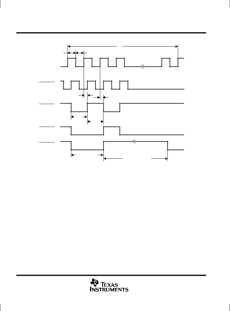
TL16C550C, TL16C550CI
ASYNCHRONOUS COMMUNICATIONS ELEMENT
WITH AUTOFLOW CONTROL
SLLS177E ± MARCH 1994 ± REVISED APRIL1998
PARAMETER MEASUREMENT INFORMATION
N
tw1 |
tw2 |
XIN
td1 


 td2
td2
BAUDOUT (1/1)
td1
td2
BAUDOUT (1/2)
tw3
tw4
BAUDOUT (1/3)
BAUDOUT (1/N)
(N > 3)
2 XIN Cycles
(N ± 2) XIN Cycles
Figure 5. Baud Generator Timing Waveforms
12 |
POST OFFICE BOX 655303 •DALLAS, TEXAS 75265 |
 Loading...