


TLC2201MJG
Texas Instruments TLC2201MJG, TLC2201MJGB, TLC2201MFKB, TLC2201IP, TLC2202BCP Datasheet
...
TLC220x, TLC220xA, TLC220xB, TLC220xY
Advanced LinCMOS LOW-NOISE PRECISION
OPERATIONAL AMPLIFIERS
SLOS175 – FEBRUARY 1997
1
POST OFFICE BOX 655303 • DALLAS, TEXAS 75265
D
B Grade Is 100% Tested for Noise
30 nV/√Hz Max at f = 10 Hz
12 nV/√Hz Max at f = 1 kHz
D
Low Input Offset Voltage . . . 500 µV Max
D
Excellent Offset Voltage Stability
With Temperature . . . 0.5 µV/°C Typ
D
Rail-to-Rail Output Swing
D
Low Input Bias Current
1 pA Typ at T
A
= 25°C
D
Common-Mode Input Voltage Range
Includes the Negative Rail
D
Fully Specified For Both Single-Supply and
Split-Supply Operation
description
The TLC220x, TLC220xA, TLC220xB, and
TLC220xY are precision, low-noise operational
amplifiers using Texas Instruments Advanced
LinCMOS process. These devices combine the
noise performance of the lowest-noise JFET
amplifiers with the dc precision available
previously only in bipolar amplifiers. The
Advanced LinCMOS process uses silicon-gate
technology to obtain input offset voltage stability
with temperature and time that far exceeds that
obtainable using metal-gate technology. In
addition, this technology makes possible input
impedance levels that meet or exceed levels
offered by top-gate JFET and expensive
dielectric-isolated devices.
The combination of excellent dc and noise
performance with a common-mode input voltage
range that includes the negative rail makes these
devices an ideal choice for high-impedance,
low-level signal-conditioning applications in either
single-supply or split-supply configurations.
The device inputs and outputs are designed to withstand –100-mA surge currents without sustaining latch-up.
In addition, internal ESD-protection circuits prevent functional failures at voltages up to 2000 V as tested under
MIL-PRF-38535, Method 3015.2; however, care should be exercised in handling these devices as exposure
to ESD may result in degradation of the parametric performance.
The C-suffix devices are characterized for operation from 0°C to 70°C. The I-suffix devices are characterized
for operation from – 40°C to 85°C. The M-suffix devices are characterized for operation over the full military
temperature range of –55°C to 125°C.
Advanced LinCMOS is a trademark of Texas Instruments Incorporated.
Copyright 1997, Texas Instruments Incorporated
On products compliant to MIL-PRF-38535, all parameters are tested
unless otherwise noted. On all other products, production
processing does not necessarily include testing of all parameters.
PRODUCTION DATA information is current as of publication date.
Products conform to specifications per the terms of Texas Instruments
standard warranty. Production processing does not necessarily include
testing of all parameters.
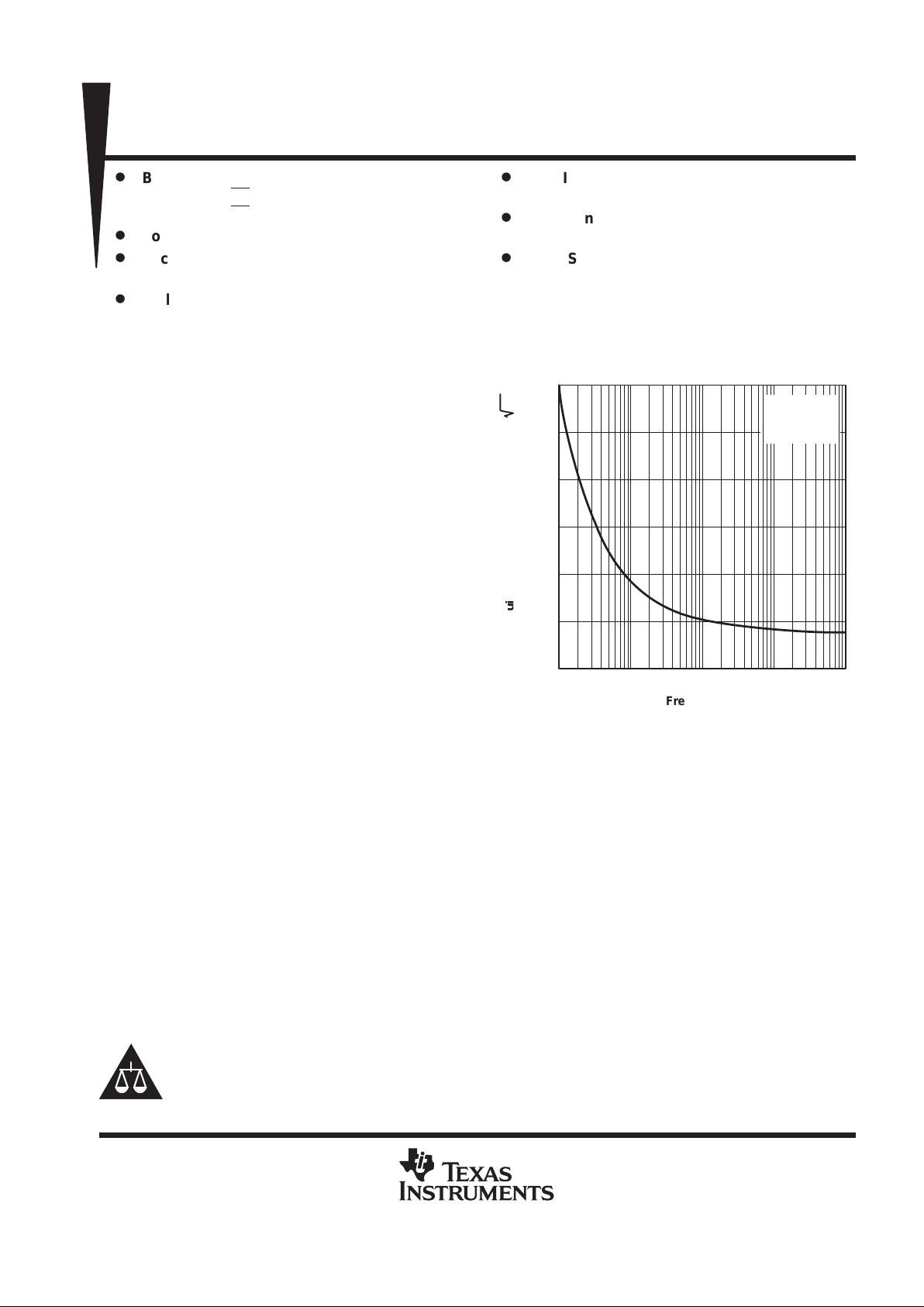
1 10 100
Vn – Equivalent Input Noise Voltage – nV/ Hz
f – Frequency – Hz
TYPICAL EQUIVALENT
INPUT NOISE VOLTAGE
vs
FREQUENCY
60
1 k 10 k
50
40
30
20
10
0
V
DD
= 5 V
R
S
= 20 Ω
T
A
= 25°C
Hz
V
n
Please be aware that an important notice concerning availability, standard warranty, and use in critical applications of
Texas Instruments semiconductor products and disclaimers thereto appears at the end of this data sheet.
TLC220x, TLC220xA, TLC220xB, TLC220xY
Advanced LinCMOS LOW-NOISE PRECISION
OPERATIONAL AMPLIFIERS
SLOS175 – FEBRUARY 1997
2
POST OFFICE BOX 655303 • DALLAS, TEXAS 75265
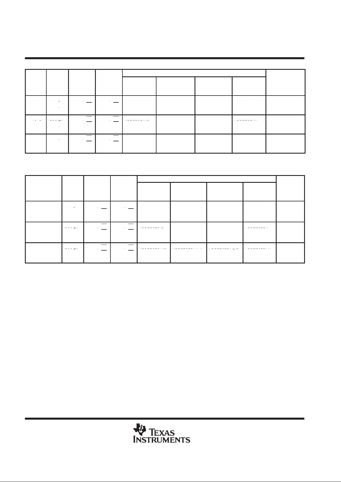
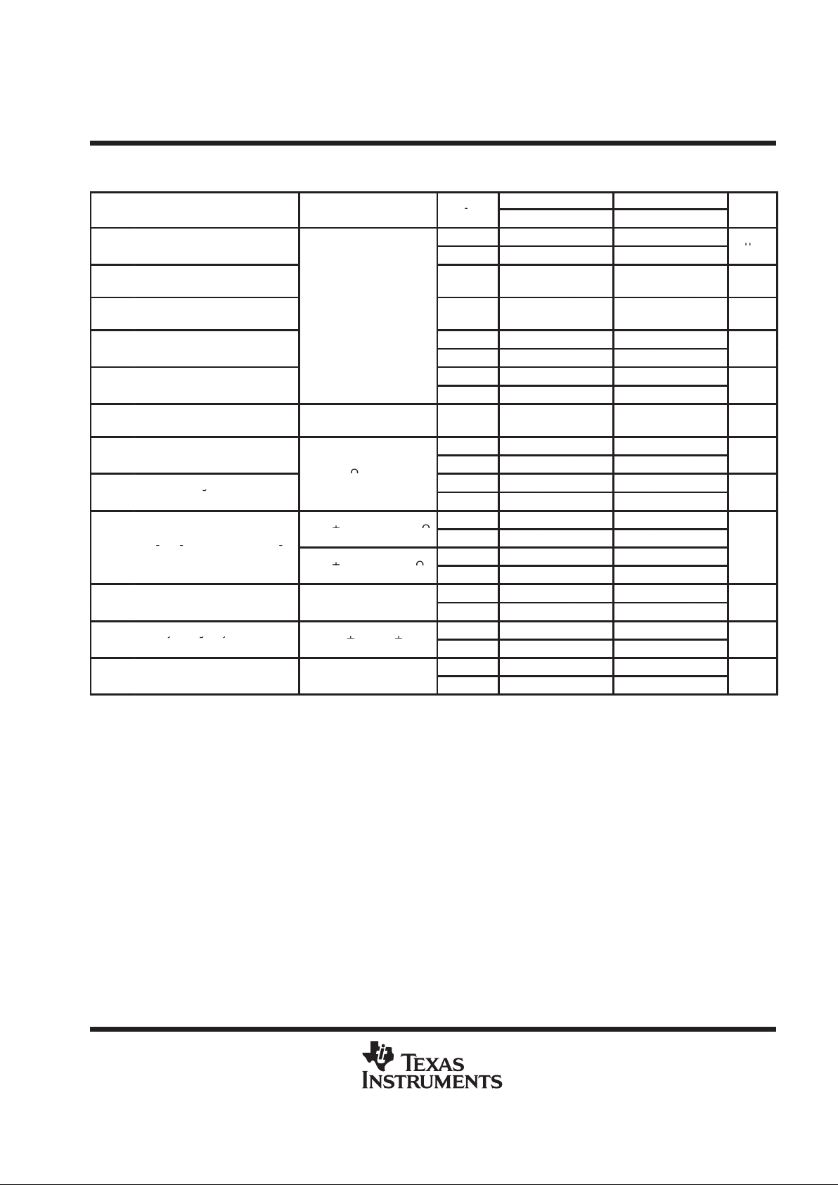
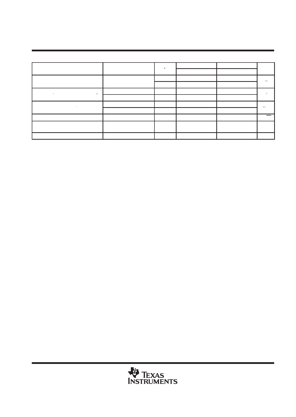
TLC2201 A VAILABLE OPTIONS
PACKAGED DEVICES
T
A
V
IO
max
AT 25°C
V
n
max
f = 10 Hz
AT 25°C
V
n
max
f = 1 kHz
AT 25°C
SMALL
OUTLINE
†
(D)
CHIP
CARRIER
(FK)
CERAMIC
DIP
(JG)
PLASTIC
DIP
(P)
CHIP
FORM
‡
(Y)
0°C 200
µ
V
35 nV/
√
Hz 15 nV/
√
Hz
TLC2201ACD TLC2201ACP
0 C
to
200
µV
200 µV
35
nV/√Hz
30 nV/√Hz
15
nV/√Hz
12 nV/√Hz
TLC2201ACD
TLC2201BCD
— —
TLC2201ACP
TLC2201BCP
TLC2201Y
70°C
µ
500 µV
— —
TLC2201CD TLC2201CP
–40°C 200
µ
V
35 nV/
√
Hz 15 nV/
√
Hz
TLC2201AID TLC2201AIP
40 C
to
200
µV
200 µV
35
nV/√Hz
30 nV/√Hz
15
nV/√Hz
12 nV/√Hz
TLC2201AID
TLC2201BID
— —
TLC2201AIP
TLC2201BIP
—
85°C
µ
500 µV
— —
TLC2201ID TLC2201IP
–55°C 200 µV
35 nV/
√
Hz 15 nV/
√
Hz
TLC2201AMD TLC2201AMFK TLC2201AMJG TLC2201AMP
to
µ
200 µV
35
nV/√Hz
30 nV/√Hz
15
nV/√Hz
12 nV/√Hz
TLC2201BMD TLC2201BMFK TLC2201BMJG TLC2201BMP
—
125°C 500 µV
— —
TLC2201MD TLC2201MFK TLC2201MJG TLC2201MP
†
The D packages are available taped and reeled. Add R suffix to device type (e.g. TLC220xBCDR).
‡
Chip forms are tested at 25°C only.
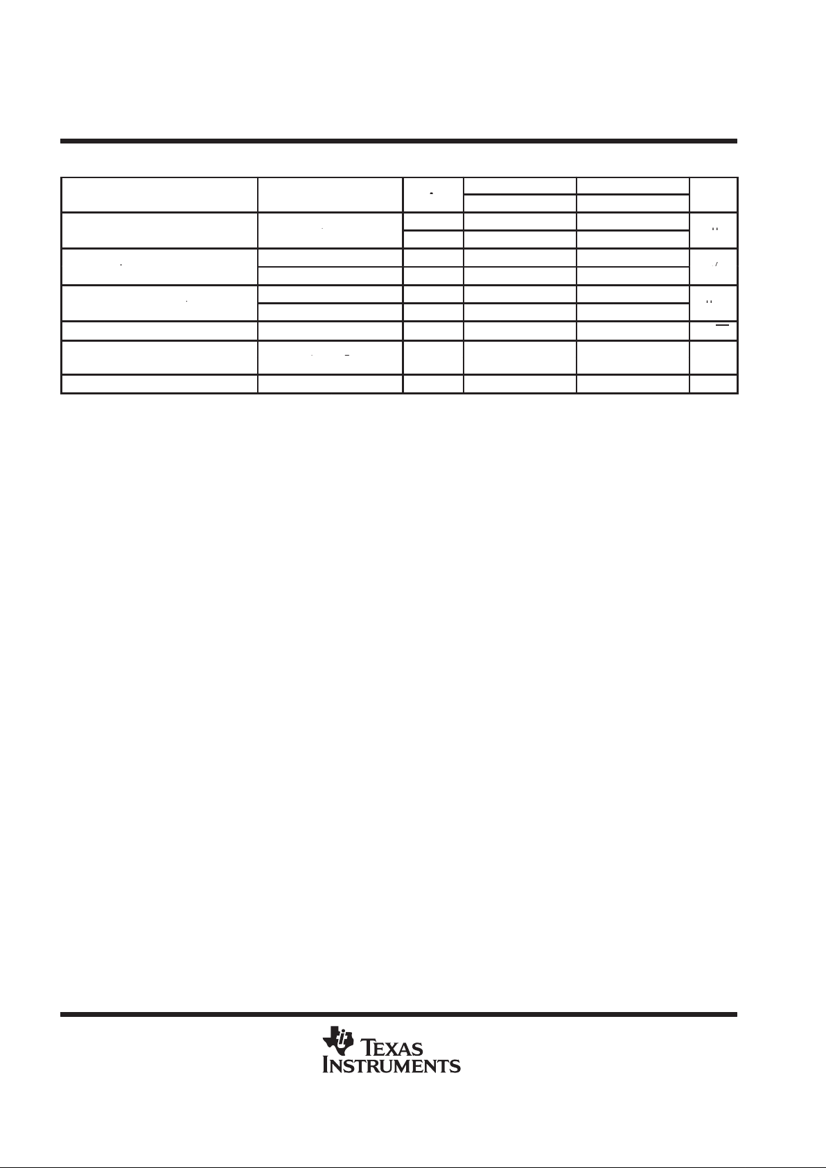
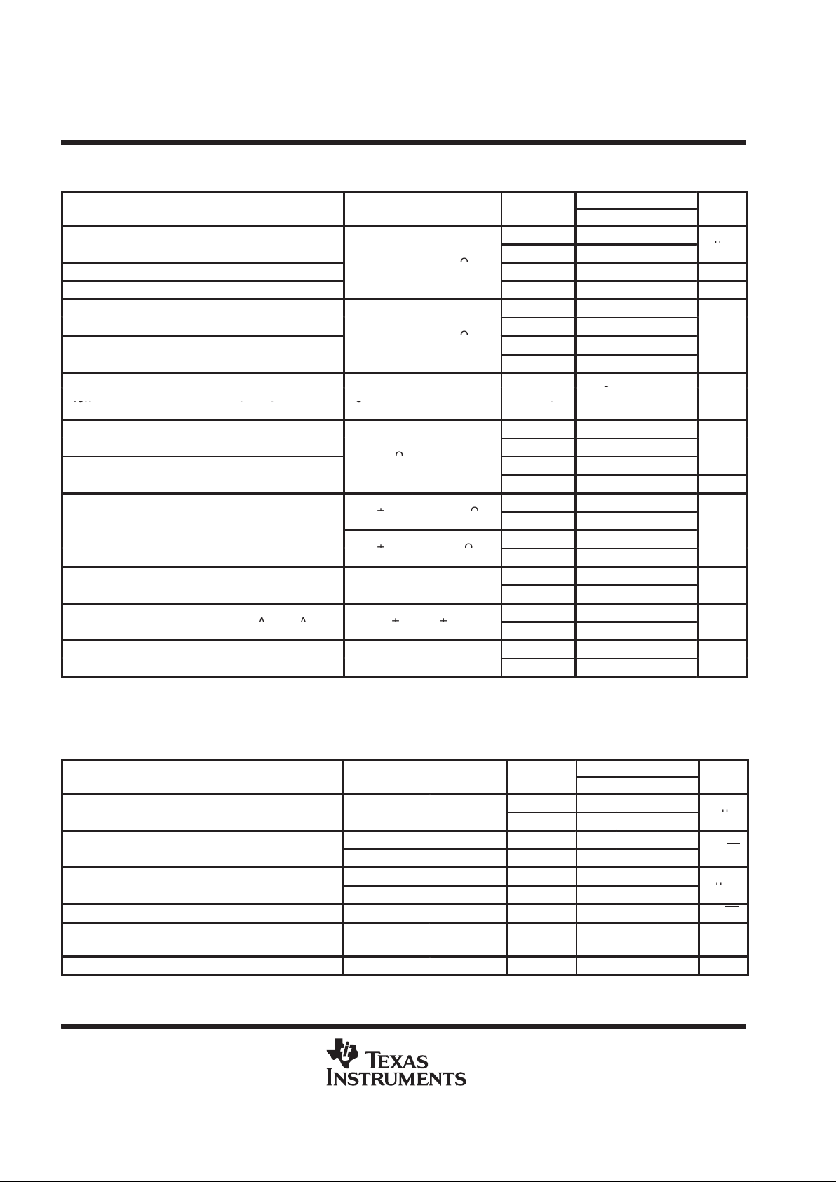
TLC2202 AVAILABLE OPTIONS
PACKAGED DEVICES
T
A
V
IO
max
AT 25°C
V
n
max
f = 10 Hz
AT 25°C
V
n
max
f = 1 kHz
AT 25°C
SMALL
OUTLINE
†
(D)
CHIP
CARRIER
(FK)
CERAMIC
DIP
(JG)
PLASTIC
DIP
(P)
CHIP
FORM
‡
(Y)
500
µ
V
30 nV/
√
Hz 12 nV/
√
Hz
TLC2202BCD — — TLC2202BCP
0°C to 70°C
500
µV
500 µV
30
nV/√Hz
35 nV/√Hz
12
nV/√Hz
15 nV/√Hz
TLC2202BCD
TLC2202ACD — —
TLC2202BCP
TLC2202ACP
TLC2202Y
1 mV
— —
TLC2202CD — — TLC2202CP
500
µ
V
30 nV/
√
Hz 12 nV/
√
Hz
TLC2202BID — — TLC2202BIP
–40°C to 85°C
500
µV
500 µV
30
nV/√Hz
35 nV/√Hz
12
nV/√Hz
15 nV/√Hz
TLC2202BID
TLC2202AID — —
TLC2202BIP
TLC2202AIP
—
1 mV
— —
TLC2202ID — — TLC2202IP
500
µ
V
30 nV/
√
Hz 12 nV/
√
Hz
TLC2202BMD TLC2202BMFK TLC2202BMJG TLC2202BMP
–55°C to 125°C
500
µV
500 µV
30
nV/√Hz
35 nV/√Hz
12
nV/√Hz
15 nV/√Hz
TLC2202BMD
TLC2202AMD
TLC2202BMFK
TLC2202AMFK
TLC2202BMJG
TLC2202AMJG
TLC2202BMP
TLC2202AMP
—
1 mV
— —
TLC2202MD TLC2202MFK TLC2202MJG TLC2202MP
†
The D packages are available taped and reeled. Add R suffix to device type (e.g. TLC220xBCDR).
‡
Chip forms are tested at 25°C only.
TLC220x, TLC220xA, TLC220xB, TLC220xY
Advanced LinCMOS LOW-NOISE PRECISION
OPERATIONAL AMPLIFIERS
SLOS175 – FEBRUARY 1997
3
POST OFFICE BOX 655303 • DALLAS, TEXAS 75265
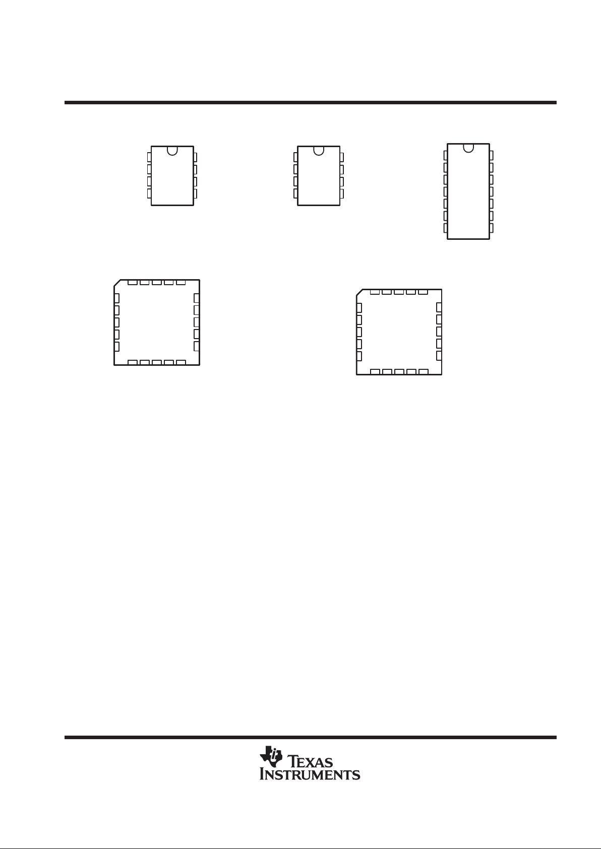
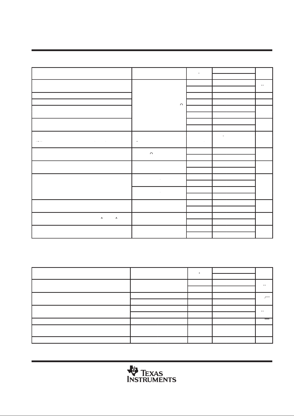
1
2
3
4
5
6
7
14
13
12
11
10
9
8
NC
NC
1OUT
1IN–
1IN+
V
DD–
/GND
NC
NC
NC
V
DD+
2OUT
2IN–
2IN+
NC
1
2
3
4
8
7
6
5
1OUT
1IN–
1IN+
V
DD–
/GND
V
DD+
2OUT
2IN–
2IN+
NC – No internal connection
3212019
910111213
4
5
6
7
8
18
17
16
15
14
NC
2OUT
NC
2IN–
NC
NC
1IN–
NC
1IN+
NC
NC
1OUT
NC
NC
NC
NC
NC
2IN+
DD+
V
DD –
V /GND
1
2
3
4
8
7
6
5
NC
IN–
IN+
V
DD–
/GND
NC
V
DD+
OUT
NC
3 2 1 20 19
910111213
4
5
6
7
8
18
17
16
15
14
NC
V
DD+
NC
OUT
NC
NC
IN–
NC
IN+
NC
NC
NC
NC
NC
NC
NC
NC
DD –
V
NC
NC
/GND
TLC2201
FK PACKAGE
(TOP VIEW)
TLC2202
D PACKAGE
(TOP VIEW)
TLC2202
JG OR P PACKAGE
(TOP VIEW)
TLC2202
FK PACKAGE
(TOP VIEW)
TLC2201
D, JG, OR P PACKAGE
(TOP VIEW)
TLC220x, TLC220xA, TLC220xB, TLC220xY
Advanced LinCMOS LOW-NOISE PRECISION
OPERATIONAL AMPLIFIERS
SLOS175 – FEBRUARY 1997
4
POST OFFICE BOX 655303 • DALLAS, TEXAS 75265
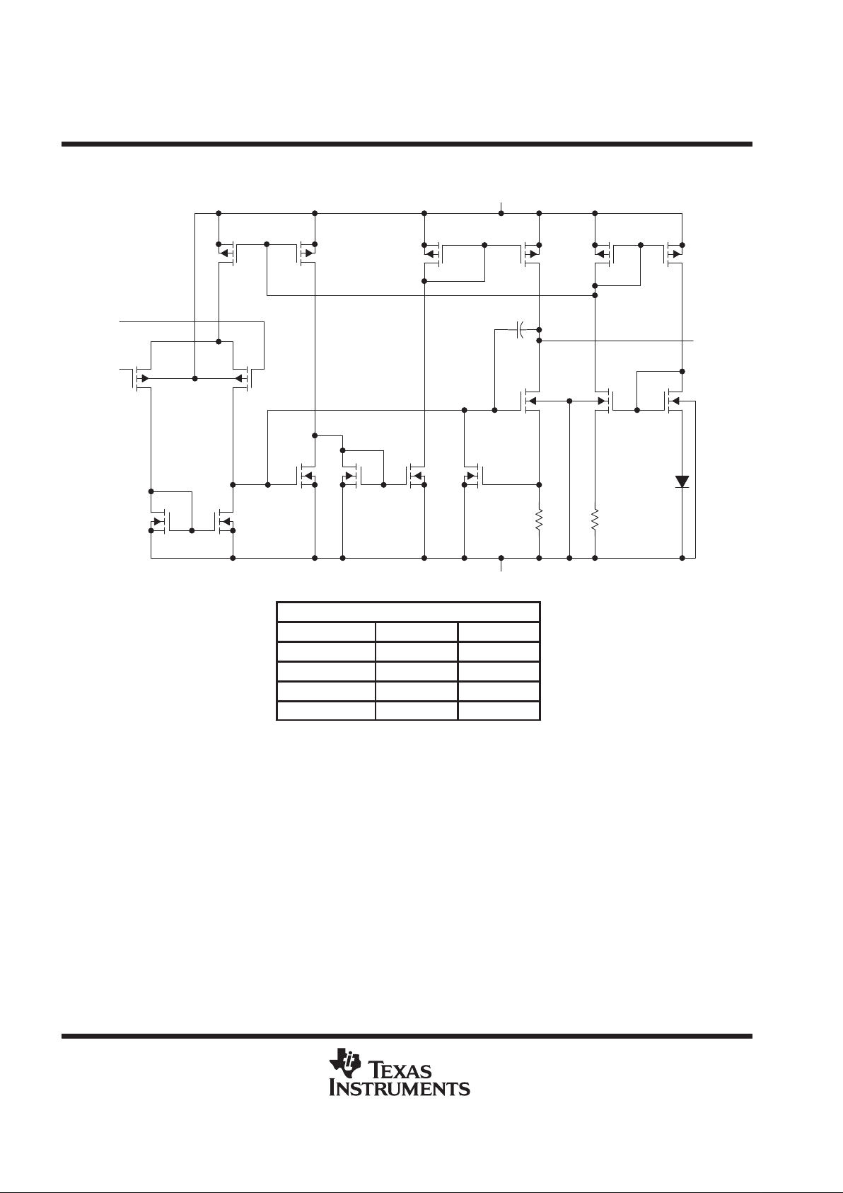
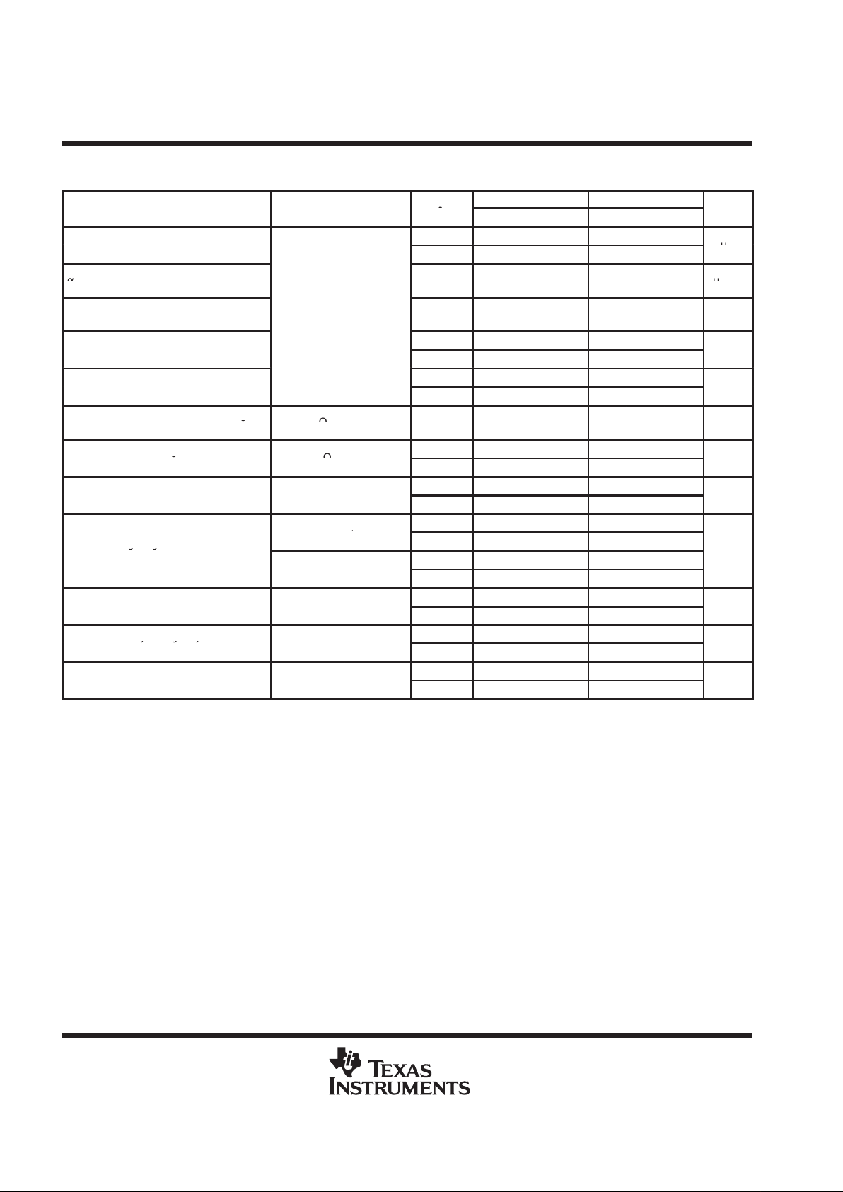
equivalent schematic (each amplifier)
IN +
IN –
Q3 Q6 Q9 Q12 Q14 Q16
Q13 Q15 Q17
Q7
Q8 Q10 Q11
Q2 Q5
Q1 Q4
R1 R2
D1
C1
V
DD+
V
DD–
/GND
OUT
ACTUAL DEVICE COMPONENT COUNT
COMPONENT TLC2201 TLC2202
Transistors 17 34
Resistors 2 2
Diodes 1 4
Capacitors 1 2
TLC220x, TLC220xA, TLC220xB, TLC220xY
Advanced LinCMOS LOW-NOISE PRECISION
OPERATIONAL AMPLIFIERS
SLOS175 – FEBRUARY 1997
5
POST OFFICE BOX 655303 • DALLAS, TEXAS 75265
TLC2201Y chip information
This chip, when properly assembled, displays characteristics similar to the TLC2201C. Thermal compression
or ultrasonic bonding may be used on the doped-aluminum bonding path. Chips may be mounted with
conductive epoxy or a gold-silicon preform.
BONDING PAD ASSIGNMENTS
CHIP THICKNESS: 15 MILS TYPICAL
BONDING PADS: 4 × 4 MILS MINIMUM
T
J
max = 150°C
TOLERANCES ARE ±10%.
ALL DIMENSIONS ARE IN MILS.
PIN (4) IS INTERNALLY CONNECTED
TO BACK SIDE OF CHIP.
TERMINAL NUMBERS ARE FOR THE
D, JG, AND P PACKAGES.
+
–
OUT
IN–
IN+
V
DD+
(7)
(2)
(3)
(6)
(4)
V
DD–
65
77
(2) (3) (4)
(6)(7)(8)
(1)
TLC220x, TLC220xA, TLC220xB, TLC220xY
Advanced LinCMOS LOW-NOISE PRECISION
OPERATIONAL AMPLIFIERS
SLOS175 – FEBRUARY 1997
6
POST OFFICE BOX 655303 • DALLAS, TEXAS 75265
TLC2202Y chip formation
This chip, when properly assembled, displays characteristics similar to the TLC2202C. Thermal compression
or ultrasonic bonding may be used on the doped-aluminum bonding pads. Chips may be mounted with
conductive epoxy or a gold-silicon preform.
BONDING PAD ASSIGNMENTS
CHIP THICKNESS: 15 MILS TYPICAL
BONDING PADS: 4 × 4 MILS MINIMUM
T
J
max = 150°C
TOLERANCES ARE ±10%.
ALL DIMENSIONS ARE IN MILS.
PIN (4) IS INTERNALLY CONNECTED
TO
BACKSIDE
OF
CHIP.
+
–
1OUT
1IN+
1IN–
V
DD+
(8)
(6)
(3)
(2)
(5)
(1)
–
+
(7)
2IN+
2IN–
2OUT
(4)
V
DD–
100
80
(1)
(2) (3)
(4)
(5)
(6)(7)(8)
TLC220x, TLC220xA, TLC220xB, TLC220xY
Advanced LinCMOS LOW-NOISE PRECISION
OPERATIONAL AMPLIFIERS
SLOS175 – FEBRUARY 1997
7
POST OFFICE BOX 655303 • DALLAS, TEXAS 75265
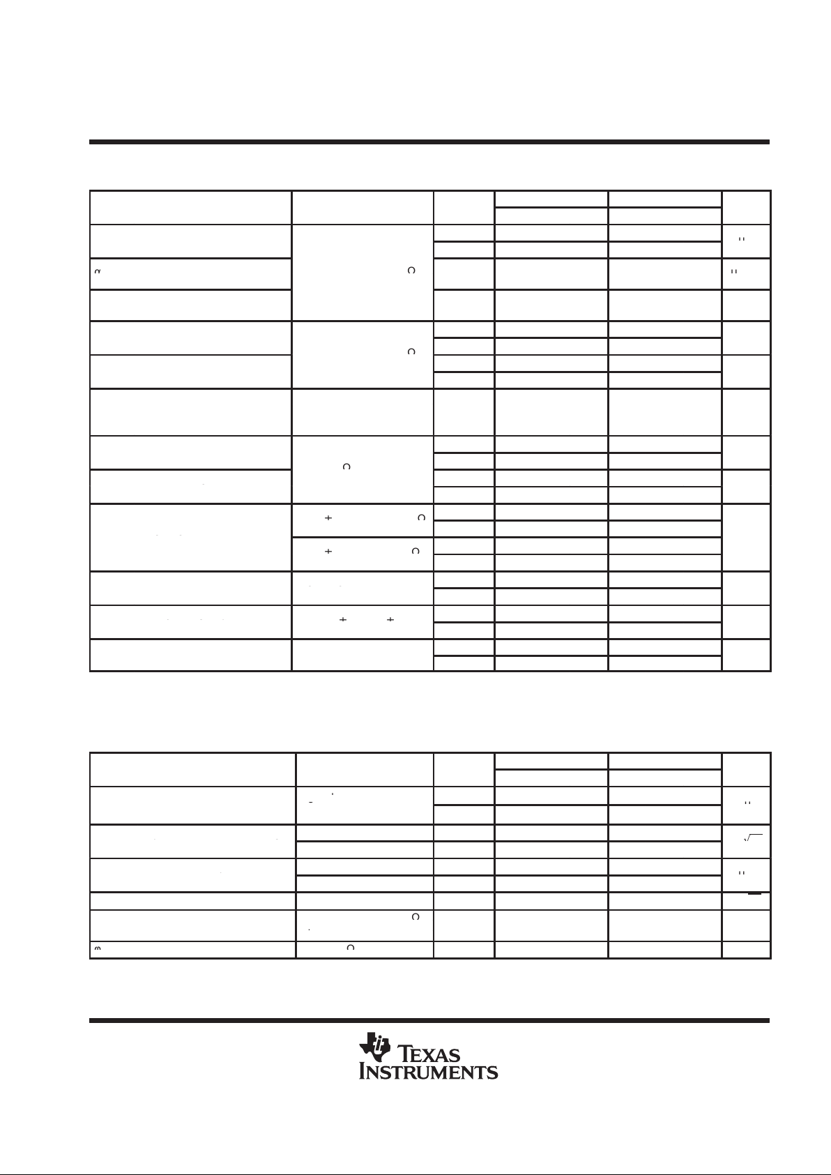
absolute maximum ratings over operating free-air temperature range (unless otherwise noted)
†
Supply voltage, V
DD+
(see Note 1) 8 V. . . . . . . . . . . . . . . . . . . . . . . . . . . . . . . . . . . . . . . . . . . . . . . . . . . . . . . . . . . .
Supply voltage, V
DD–
–8 V. . . . . . . . . . . . . . . . . . . . . . . . . . . . . . . . . . . . . . . . . . . . . . . . . . . . . . . . . . . . . . . . . . . . . .
Differential input voltage, V
ID
(see Note 2) ±16 V. . . . . . . . . . . . . . . . . . . . . . . . . . . . . . . . . . . . . . . . . . . . . . . . . . .
Input voltage, V
I
(any input) ±8 V. . . . . . . . . . . . . . . . . . . . . . . . . . . . . . . . . . . . . . . . . . . . . . . . . . . . . . . . . . . . . . . . .
Input current, I
I
(each input) ±5 mA. . . . . . . . . . . . . . . . . . . . . . . . . . . . . . . . . . . . . . . . . . . . . . . . . . . . . . . . . . . . . . .
Output current, I
O
(each output) ±50 mA. . . . . . . . . . . . . . . . . . . . . . . . . . . . . . . . . . . . . . . . . . . . . . . . . . . . . . . . . .
Duration of short-circuit current at (or below) 25°C (see Note 3) unlimited. . . . . . . . . . . . . . . . . . . . . . . . . . . . . .
Continuous total dissipation See Dissipation Rating Table. . . . . . . . . . . . . . . . . . . . . . . . . . . . . . . . . . . . . . . . . . .
Operating free-air temperature range, T
A
: C suffix 0°C to 70°C. . . . . . . . . . . . . . . . . . . . . . . . . . . . . . . . . . . . . . .
I suffix –40°C to 85°C. . . . . . . . . . . . . . . . . . . . . . . . . . . . . . . . . . . . . .
M suffix –55°C to 125°C. . . . . . . . . . . . . . . . . . . . . . . . . . . . . . . . . . . .
Storage temperature range –65°C to 150°C. . . . . . . . . . . . . . . . . . . . . . . . . . . . . . . . . . . . . . . . . . . . . . . . . . . . . . . .
Case temperature for 60 seconds: FK package 260°C. . . . . . . . . . . . . . . . . . . . . . . . . . . . . . . . . . . . . . . . . . . . . .
Lead temperature 1,6 mm (1/16 inch) from case for 10 seconds: D or P package 260°C. . . . . . . . . . . . . . . . .
Lead temperature 1,6 mm (1/16 inch) from case for 60 seconds: JG package 300°C. . . . . . . . . . . . . . . . . . . .
†
Stresses beyond those listed under “absolute maximum ratings” may cause permanent damage to the device. These are stress ratings only, and
functional operation of the device at these or any other conditions beyond those indicated under “recommended operating conditions” is not
implied. Exposure to absolute-maximum-rated conditions for extended periods may affect device reliability.
NOTES: 1. All voltage values except differential voltages are with respect to the midpoint between V
DD+
and V
DD–
.
2. Differential voltages are at IN+ with respect to IN–.
3. The output may be shorted to either supply. Temperature and/or supply voltages must be limited to ensure that the maximum
dissipation rating in not exceeded.
DISSIPATION RATING TABLE
T
≤ 25°C DERATING FACTOR T
= 70°C T
= 85°C T
= 125°C
PACKAGE
A
POWER RATING ABOVE T
A
= 25°C
A
POWER RATING
A
POWER RATING
A
POWER RATING
D–8 725 mW 5.8 mW/°C 464 mW 377 mW 145 mW
D–14 950 mW 7.6 mW/°C 608 mW 494 mW 190 mW
FK 1375 mW 11.0 mW/°C 880 mW 715 mW 275 mW
JG 1050 mW 8.4 mW/°C 672 mW 546 mW 210 mW
P 1000 mW 8.0 mW/°C 640 mW 520 mW 200 mW
recommended operating conditions
C SUFFIX I SUFFIX M SUFFIX
MIN MAX MIN MAX MIN MAX
UNIT
Supply voltage, V
DD
± ±2.3 ±8 ±2.3 ±8 ±2.3 ±8 V
Common-mode input voltage, V
IC
V
DD–
V
DD+
–2.3 V
DD–
V
DD+
–2.3 V
DD–
V
DD+
–2.3 V
Operating free-air temperature, T
A
0 70 –40 85 –55 125 °C
TLC220x, TLC220xA, TLC220xB, TLC220xY
Advanced LinCMOS LOW-NOISE PRECISION
OPERATIONAL AMPLIFIERS
SLOS175 – FEBRUARY 1997
8
POST OFFICE BOX 655303 • DALLAS, TEXAS 75265
TLC2201C electrical characteristics at specified free-air temperature, V
DD±
= ±5 V (unless
otherwise noted)
TLC2201C
PARAMETER
TEST
CONDITIONS
T
A
†
MIN TYP MAX
UNIT
p
25°C 100 500
V
IO
Inp
u
t
offset
v
oltage
Full range 600
µ
V
p
p
α
VIO
Temperat
u
re
coefficient
of
inp
u
t
offset
v
oltage
F
u
ll
range
0
.
5
µ
V/°C
Input offset voltage long-term drift (see Note 4)
25°C 0.001 0.005 µV/mo
p
V
IC
=
0
,
R
S
=
50
Ω
25°C 0.5
p
I
IO
Inp
u
t
offset
c
u
rrent
Full range 100
pA
p
25°C 1
p
I
IB
Inp
u
t
bias
c
u
rrent
Full range 100
pA
–5
V
ICR
Common-mode input voltage range R
S
= 50 Ω Full range
5
to
V
ICR
gg
S
g
2.7
p
p
p
25°C 4.7 4.8
V
OM+
Ma
x
im
u
m
positi
v
e
peak
o
u
tp
u
t
v
oltage
s
w
ing
Full range 4.7
V
p
p
R
L
=
10
kΩ
25°C –4.7 –4.9
V
OM–
Ma
x
im
u
m
negati
v
e
peak
o
u
tp
u
t
v
oltage
s
w
ing
Full range –4.7
V
25°C 400 560
p
V
O
=
±4
V
,
R
L
=
500
kΩ
Full range 300
A
VD
Large
-
signal
differential
v
oltage
amplification
25°C 90 100
V/mV
V
O
=
±4
V
,
R
L
=
10
kΩ
Full range 70
V
= V
min, V
= 0,
CMRR
Common
-
mode
rejection
ratio
IC ICR
,
R
S
= 50 Ω
O
,
F
u
ll
range
85
dB
pp
25°C 90 110
k
SVR
S
u
ppl
y v
oltage
rejection
ratio
(∆V
DD±
/∆V
IO
)
V
DD±
=
±2
.
3
V
to
±8
V
Full range 85
dB
pp
25°C 1.1 1.5
I
DD
S
u
ppl
y
c
u
rrent
V
O
=
0
,
No
load
Full range 1.5
mA
†
Full range is 0°C to 70°C.
NOTE 4: Typical values are based on the input offset voltage shift observed through 168 hours of operating life test at T
A
= 150°C extrapolated
to T
A
= 25°C using the Arrhenius equation and assuming an activation energy of 0.96 eV .
TLC2201C operating characteristics at specified free-air temperature, V
DD±
= ±5 V
TLC2201C
PARAMETER
TEST
CONDITIONS
T
A
†
MIN TYP MAX
UNIT
V
O
= ±2.3 V , R
L
= 10 kΩ,
25°C 2 2.7
SR
Sle
w
rate
at
u
nit
y
gain
C
L
= 100 pF
Full range 1.5
V/
µ
s
p
f = 10 Hz 25°C 18
V
n
Eq
u
i
v
alent
inp
u
t
noise
v
oltage
f = 1 kHz 25°C 8
n
V/√H
z
p
p
f = 0.1 to 1 Hz 25°C 0.5
V
N(PP)
Peak
-
to
-
peak
eq
u
i
v
alent
inp
u
t
noise
v
oltage
f = 0.1 to 10 Hz 25°C 0.7
µ
V
I
n
Equivalent input noise current 25°C 0.6 fA/√Hz
p
f = 10 kHz, R
L
= 10 kΩ,
°
Gain
-
band
w
idth
prod
u
ct
C
L
= 100 pF
L
25°C
1
.
9
MH
z
φ
m
Phase margin at unity gain R
L
= 10 kΩ, C
L
= 100 pF 25°C 48°
†
Full range is 0°C to 70°C.
TLC220x, TLC220xA, TLC220xB, TLC220xY
Advanced LinCMOS LOW-NOISE PRECISION
OPERATIONAL AMPLIFIERS
SLOS175 – FEBRUARY 1997
9
POST OFFICE BOX 655303 • DALLAS, TEXAS 75265
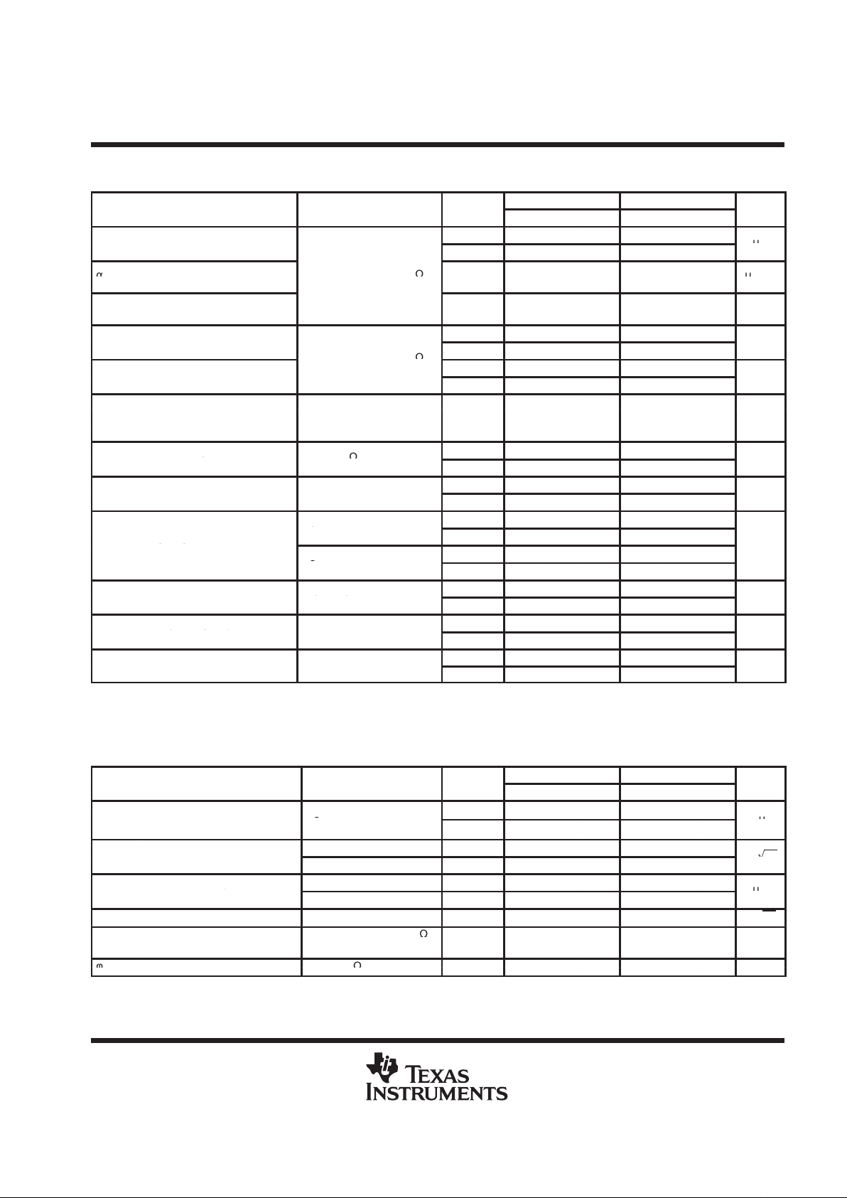
TLC2201C electrical characteristics at specified free-air temperature, V
DD±
= ±5 V (unless
otherwise noted)
TLC2201AC TLC2201BC
PARAMETER
TEST
CONDITIONS
T
A
†
MIN TYP MAX MIN TYP MAX
UNIT
p
25°C 80 200 80 200
V
IO
Inp
u
t
offset
v
oltage
Full range 300 300
µ
V
α
VIO
Temperature coefficient of input
offset voltage
Full range 0.5 0.5 µV/°C
Input offset voltage long-term
drift (see Note 4)
V
IC
= 0, R
S
= 50 Ω
25°C
0.001 0.005 0.001 0.005 µV/mo
p
25°C 0.5 0.5
p
I
IO
Inp
u
t
offset
c
u
rrent
Full range 100 100
pA
p
25°C 1 1
p
I
IB
Inp
u
t
bias
c
u
rrent
Full range 100 100
pA
V
ICR
Common-mode input voltage
range
R
S
= 50 Ω Full range
–5 to
2.7
–5 to
2.7
V
Maximum positive peak output
25°C 4.7 4.8 4.7 4.8
V
OM+
voltage swing
Full range 4.7 4.7
V
Maximum negative peak output
R
L
=
10
kΩ
25°C –4.7 –4.9 –4.7 –4.9
V
OM–
g
voltage swing
Full range –4.7 –4.7
V
25°C 400 560 400 560
Large-signal differential voltage
V
O
=
±4
V
,
R
L
=
500
kΩ
Full range 300 300
A
VD
gg g
amplification
25°C 90 100 90 100
V/mV
V
O
=
±4
V
,
R
L
=
10
kΩ
Full range 70 70
V
IC
= V
ICR
min, 25°C 90 115 90 115
CMRR
Common
-
mode
rejection
ratio
V
O
= 0, R
S
= 50 Ω Full range 85 85
dB
Supply voltage rejection ratio
25°C 90 110 90 110
k
SVR
ygj
(∆V
DD±
/∆V
IO
)
V
DD±
=
±2
.
3
V
to
±8
V
Full range 85 85
dB
pp
25°C 1.1 1.5 1.1 1.5
I
DD
S
u
ppl
y
c
u
rrent
V
O
=
0
,
No
load
Full range 1.5 1.5
mA
†
Full range is 0°C to 70°C.
NOTE 4: Typical values are based on the input offset voltage shift observed through 168 hours of operating life test at T
A
= 150°C extrapolated
to T
A
= 25°C using the Arrhenius equation and assuming an activation energy of 0.96 eV .
TLC220x, TLC220xA, TLC220xB, TLC220xY
Advanced LinCMOS LOW-NOISE PRECISION
OPERATIONAL AMPLIFIERS
SLOS175 – FEBRUARY 1997
10
POST OFFICE BOX 655303 • DALLAS, TEXAS 75265
TLC2201C operating characteristics at specified free-air temperature, V
DD±
= ±5 V
TLC2201AC TLC2210BC
PARAMETER
TEST
CONDITIONS
T
A
†
MIN TYP MAX MIN TYP MAX
UNIT
V
= ±2.3 V ,
R
L
= 10 kΩ,
25°C 2 2.7 2 2.7
SR
Sle
w
rate
at
u
nit
y
gain
O
,
C
L
= 100 pF
Full range 1.5 1.5
V/
µ
s
Equivalent input noise volt-
f = 10 Hz 25°C 18 35 18 30
V
n
q
age (see Note 5)
f = 1 kHz
25°C 8 15 8 12
n
V/√H
z
Peak-to-peak equivalent input
f = 0.1 to 1 Hz 25°C 0.5 0.5
V
N(PP)
q
noise voltage
f = 0.1 to 10 Hz
25°C 0.7 0.7
µ
V
I
n
Equivalent input noise current 25°C 0.6 0.6
fA/√Hz
p
f = 10 kHz,
R
L
= 10 kΩ,
°
Gain
-
band
w
idth
prod
u
ct
,
C
L
= 100 pF
L
25°C
1
.
9
1
.
9
MH
z
φ
m
Phase margin at unity gain R
L
= 10 kΩ, C
L
= 100 pF 25°C 48° 48°
†
Full range is 0°C to 70°C.
NOTE 5: This parameter is tested on a sample basis for the TLC2201A and on all devices for the TLC2201B. For other test requirements, please
contact the factory. This statement has no bearing on testing or nontesting of other parameters.
TLC220x, TLC220xA, TLC220xB, TLC220xY
Advanced LinCMOS LOW-NOISE PRECISION
OPERATIONAL AMPLIFIERS
SLOS175 – FEBRUARY 1997
11
POST OFFICE BOX 655303 • DALLAS, TEXAS 75265
TLC2201C electrical characteristics at specified free-air temperature, V
DD
= 5 V (unless otherwise
noted)
TLC2201C
PARAMETER
TEST
CONDITIONS
T
A
†
MIN TYP MAX
UNIT
p
25°C 100 500
V
IO
Inp
u
t
offset
v
oltage
Full range 600
µ
V
α
VIO
Temperature coefficient of input offset voltage Full range 0.5 µV/°C
Input offset voltage long-term drift (see Note 4)
25°C 0.001 0.005 µV/mo
p
V
IC
=
0
,
R
S
=
50
Ω
25°C 0.5
p
I
IO
Inp
u
t
offset
c
u
rrent
Full range 100
pA
p
25°C 1
p
I
IB
Inp
u
t
bias
c
u
rrent
Full range 100
pA
0
V
ICR
Common-mode input voltage range R
S
= 50 Ω Full range
0
to
V
ICR
gg
S
g
2.7
p
25°C 4.7 4.8
V
OH
Ma
x
im
u
m
high
-
le
v
el
o
u
tp
u
t
v
oltage
R
L
=
10
kΩ
Full range 4.7
V
p
25°C 0 50
V
OL
Ma
x
im
u
m
lo
w-
le
v
el
o
u
tp
u
t
v
oltage
I
O
=
0
Full range 50
mV
V
= 1 V to 4 V,
25°C 150 315
p
O
,
R
L
= 500 kΩ
Full range 100
A
VD
Large
-
signal
differential
v
oltage
amplification
V
= 1 V to 4 V,
25°C 25 55
V/mV
O
,
R
L
= 10 kΩ
Full range 15
V
= V
min, V
= 0,
25°C 90 110
CMRR
Common
-
mode
rejection
ratio
IC ICR
,
R
S
= 50 Ω
O
,
Full range 85
dB
pp
25°C 90 110
k
SVR
S
u
ppl
y v
oltage
rejection
ratio
(∆V
DD±
/∆V
IO
)
V
DD
=
4
.
6
V
to
16
V
Full range 85
dB
pp
25°C 1 1.5
I
DD
S
u
ppl
y
c
u
rrent
V
O
=
2
.
5
V
,
No
load
Full range 1.5
mA
†
Full range is 0°C to 70°C.
NOTE 4: Typical values are based on the input offset voltage shift observed through 168 hours of operating life test at T
A
= 150°C extrapolated
to T
A
= 25°C using the Arrhenius equation and assuming an activation energy of 0.96 eV .
TLC2201C operating characteristics at specified free-air temperature, V
DD
= 5 V
TLC2201C
PARAMETER
TEST
CONDITIONS
T
A
†
MIN TYP MAX
UNIT
V
O
= 0.5 V to 2.5 V, 25°C 1.8 2.5
SR
Sle
w
rate
at
u
nit
y
gain
R
L
= 10 kΩ, C
L
= 100 pF Full range 1.3
V/
µ
s
p
f = 10 Hz 25°C 18
V
n
Eq
u
i
v
alent
inp
u
t
noise
v
oltage
f = 1 kHz 25°C 8
n
V/√H
z
p
p
f = 0.1 to 1 Hz 25°C 0.5
V
N(PP)
Peak
-
to
-
peak
eq
u
i
v
alent
inp
u
t
noise
v
oltage
f = 0.1 to 10 Hz 25°C 0.7
µ
V
I
n
Equivalent input noise current 25°C 0.6 fA/√Hz
p
f = 10 kHz, R
L
= 10 kΩ,
°
Gain
-
band
w
idth
prod
u
ct
C
L
= 100 pF
L
25°C
1
.
8
MH
z
φ
m
Phase margin at unity gain R
L
= 10 kΩ, C
L
= 100 pF 25°C 45°
†
Full range is 0°C to 70°C.
TLC220x, TLC220xA, TLC220xB, TLC220xY
Advanced LinCMOS LOW-NOISE PRECISION
OPERATIONAL AMPLIFIERS
SLOS175 – FEBRUARY 1997
12
POST OFFICE BOX 655303 • DALLAS, TEXAS 75265
TLC2201C electrical characteristics at specified free-air temperature, V
DD
= 5 V (unless otherwise
noted)
TLC2201AC TLC2201BC
PARAMETER
TEST
CONDITIONS
T
A
†
MIN TYP MAX MIN TYP MAX
UNIT
p
25°C 80 200 80 200
V
IO
Inp
u
t
offset
v
oltage
Full range 300 300
µ
V
T emperature coef ficient of
°
α
VIO
input offset voltage
F
u
ll
range
0
.
5
0
.
5
µ
V/°C
Input offset voltage long-term
drift (see Note 4)
V
IC
= 0, R
S
= 50 Ω
25°C
0.001 0.005 0.001 0.005 µV/mo
p
25°C 0.5 0.5
p
I
IO
Inp
u
t
offset
c
u
rrent
Full range 100 100
pA
p
25°C 1 1
p
I
IB
Inp
u
t
bias
c
u
rrent
Full range 100 100
pA
Common-mode input voltage
0 to 0 to
V
ICR
g
range
R
S
=
50
Ω
F
u
ll
range
2.7 2.7
V
Maximum high-level output
25°C 4.7 4.8 4.7 4.8
V
OH
g
voltage
R
L
=
10
kΩ
Full range 4.7 4.7
V
Maximum low-level output
25°C 0 50 0 50
V
OL
voltage
I
O
=
0
Full range 50 50
mV
V
= 1 V to 4 V,
25°C 150 315 150 315
Large-signal differential
O
,
R
L
= 500 kΩ
Full range 100 100
A
VD
gg
voltage amplification
V
= 1 V to 4 V,
25°C 25 55 25 55
V/mV
O
,
R
L
= 10 kΩ
Full range 15 15
V
IC
= V
ICR
min, 25°C 90 110 90 110
CMRR
Common
-
mode
rejection
ratio
V
O
= 0, R
S
= 50 Ω Full range 85 85
dB
Supply voltage rejection ratio
25°C 90 110 90 110
k
SVR
ygj
(∆V
DD±
/∆V
IO
)
V
DD
=
4
.
6
V
to
16
V
Full range 85 85
dB
pp
25°C 1 1.5 1 1.5
I
DD
S
u
ppl
y
c
u
rrent
V
O
=
2
.
5
V
,
No
load
Full range 1.5 1.5
mA
†
Full range is 0°C to 70°C.
NOTE 4: Typical values are based on the input offset voltage shift observed through 168 hours of operating life test at T
A
= 150°C extrapolated
to T
A
= 25°C using the Arrhenius equation and assuming an activation energy of 0.96 eV .
TLC220x, TLC220xA, TLC220xB, TLC220xY
Advanced LinCMOS LOW-NOISE PRECISION
OPERATIONAL AMPLIFIERS
SLOS175 – FEBRUARY 1997
13
POST OFFICE BOX 655303 • DALLAS, TEXAS 75265
TLC2201C operating characteristics at specified free-air temperature, V
DD
= 5 V
TLC2201AC TLC2210BC
PARAMETER
TEST
CONDITIONS
T
A
†
MIN TYP MAX MIN TYP MAX
UNIT
V
O
= 0.5 V to 2.5 V, 25°C 1.8 2.5 1.8 2.5
SR
Sle
w
rate
at
u
nit
y
gain
R
L
= 10 kΩ, C
L
= 100 pF Full range 1.3 1.3
V/
µ
s
Equivalent input noise voltage
f = 10 Hz 25°C 18 35 18 30
V
n
qg
(see Note 5)
f = 1 kHz
25°C 8 15 8 12
n
V/√H
z
Peak-to-peak equivalent input
f = 0.1 to 1 Hz 25°C 0.5 0.5
V
N(PP)
q
noise voltage
f = 0.1 to 10 Hz
25°C 0.7 0.7
µ
V
I
n
Equivalent input noise current 25°C 0.6 0.6
fA/√Hz
Gain-bandwidth product
f = 10 kHz,
C
L
= 100 pF
R
L
= 10 kΩ,
25°C 1.8 1.8 MHz
φ
m
Phase margin at unity gain R
L
= 10 kΩ, C
L
= 100 pF 25°C 45° 45°
†
Full range is 0°C to 70°C.
NOTE 5: This parameter is tested on a sample basis for the TLC2201A and on all devices for the TLC2201B. For other test requirements, please
contact the factory. This statement has no bearing on testing or nontesting of other parameters.
TLC220x, TLC220xA, TLC220xB, TLC220xY
Advanced LinCMOS LOW-NOISE PRECISION
OPERATIONAL AMPLIFIERS
SLOS175 – FEBRUARY 1997
14
POST OFFICE BOX 655303 • DALLAS, TEXAS 75265
TLC2202C electrical characteristics at specified free-air temperature, V
DD±
= ±5 V (unless
otherwise specified)
TLC2202C
PARAMETER
TEST
CONDITIONS
T
A
†
MIN TYP MAX
UNIT
p
25°C 100 1000
V
IO
Inp
u
t
offset
v
oltage
Full range 1150
µ
V
α
VIO
Temperature coefficient of input offset voltage
V
IC
=
0
,
R
S
=
50
Ω
Full range 0.5 µV/°C
Input offset voltage long-term drift (see Note 4) 25°C 0.001 0.005 µV/mo
p
25°C 0.5
I
IO
Inp
u
t
offset
c
u
rrent
Full range 100
p
p
V
IC
=
0
,
R
S
=
50
Ω
25°C 1
pA
I
IB
Inp
u
t
bias
c
u
rrent
Full range 100
–5
V
ICR
Common-mode input voltage range R
S
= 50 Ω Full range
5
to
V
ICR
gg
S
g
2.7
p
p
p
25°C 4.7 4.8
V
OM+
Ma
x
im
u
m
positi
v
e
peak
o
u
tp
u
t
v
oltage
s
w
ing
Full range 4.7
V
p
p
R
L
=
10
kΩ
25°C –4.7 –4.9
V
OM–
Ma
x
im
u
m
negati
v
e
peak
o
u
tp
u
t
v
oltage
s
w
ing
Full range –4.7 V
25°C 300 560
p
V
O
=
±4
V
,
R
L
=
500
kΩ
Full range 200
A
VD
Large
-
signal
differential
v
oltage
amplification
25°C 50 100
V/mV
V
O
=
±4
V
,
R
L
=
10
kΩ
Full range 25
V
= 0, V
= V
min,
25°C 80 115
CMRR
Common
-
mode
rejection
ratio
O
,
IC ICR
,
R
S
= 50 Ω
Full range 80
dB
pp
25°C 80 110
k
SVR
S
u
ppl
y-v
oltage
rejection
ratio
(∆V
DD±
/∆V
IO
)
V
DD±
=
±2
.
3
V
to
±8
V
Full range 80
dB
pp
25°C 1.8 2.7
I
DD
S
u
ppl
y
c
u
rrent
V
O
=
0
,
No
load
Full range 2.7
mA
†
Full range is 0°C to 70°C.
NOTE 4: Typical values are based on the input offset voltage shift observed through 168 hours of operating life test at T
A
= 150°C extrapolated
to T
A
= 25°C using the Arrhenius equation and assuming an activation energy of 0.96 eV .
TLC2202C operating characteristics at specified free-air temperature, V
DD±
= ±5 V
TLC2202C
PARAMETER
TEST
CONDITIONS
T
A
†
MIN TYP MAX
UNIT
V
= ±2.3 V , R
= 10 kΩ,
25°C 1.8 2.7
SR
Sle
w
rate
at
u
nit
y
gain
O
,
C
L
= 100 pF
L
,
Full range 1.3
V/
µ
s
p
f = 10 Hz 25°C 18
V
n
Eq
u
i
v
alent
inp
u
t
noise
v
oltage
f = 1 kHz 25°C 8
n
V/√H
z
p
p
f = 0.1 to 1 Hz 25°C 0.5
V
N(PP)
Peak
-
to
-
peak
eq
u
i
v
alent
inp
u
t
noise
v
oltage
f = 0.1 to 10 Hz 25°C 0.7
µ
V
I
n
Equivalent input noise current 25°C 0.6 fA/√Hz
p
f = 10 kHz, R
= 10 kΩ,
°
Gain
-
band
w
idth
prod
u
ct
,
C
L
= 100 pF
L
,
25°C
1
.
9
MH
z
φ
m
Phase margin at unity gain R
L
= 10 kΩ, C
L
= 100 pF 25°C 48°
†
Full range is 0°C to 70°C.
TLC220x, TLC220xA, TLC220xB, TLC220xY
Advanced LinCMOS LOW-NOISE PRECISION
OPERATIONAL AMPLIFIERS
SLOS175 – FEBRUARY 1997
15
POST OFFICE BOX 655303 • DALLAS, TEXAS 75265
TLC2202C electrical characteristics at specified free-air temperature, V
DD±
= ±5 V (unless
otherwise noted)
TLC2202AC TLC2202BC
PARAMETER
TEST
CONDITIONS
T
A
†
MIN TYP MAX MIN TYP MAX
UNIT
p
25°C 80 500 80 500
V
IO
In ut
offset
voltage
Full range 650 650
µV
T emperature coef ficient
°
α
VIO
of input offset voltage
V
IC
=
0
,
R
S
=
50
Ω
Full
range
0
.
5
0
.
5
µV/°C
Input offset voltage long-term
drift (see Note 4)
25°C 0.001 0.005 0.001 0.005 µV/mo
p
25°C 0.5 0.5
p
I
IO
In ut
offset
current
Full range 100 100
A
p
V
IC
=
0
,
R
S
=
50
Ω
25°C 1 1
p
I
IB
In ut
bias
current
Full range 100 100
A
p
–5 –5
V
ICR
Common
-
mode
inp
u
t
v
oltage
R
S
= 50 Ω Full range
to to
V
range
2.7 2.7
Maximum positive peak
25°C 4.7 4.8 4.7 4.8
V
OM
+
output voltage swing
Full range 4.7 4.7
V
Maximum negative peak
R
L
=
10
kΩ
25°C –4.7 –4.9 –4.7 –4.9
V
OM
–
g
output voltage swing
Full range –4.7 –4.7
V
25°C 300 560 300 560
Large-signal differential
V
O
=
±4
V
,
R
L
=
500
kΩ
Full range 200 200
A
VD
gg
voltage amplification
25°C 50 100 50 100
V/mV
V
O
=
±4
V
,
R
L
=
10
kΩ
Full range 25 25
V
IC
= V
ICR
min,
25°C 80 115 80 115
CMRR
Common
-
mode
rejection
ratio
IC ICR
V
O
= 0, R
S
= 50 Ω
Full range 80 80
dB
Supply-voltage rejection ratio
25°C 80 110 80 110
k
SVR
ygj
(∆V
DD±
/∆V
IO
)
V
DD
±
=
±2
.
3
V
to
±8
V
Full range 80 80
dB
pp
25°C 1.8 2.7 1.8 2.7
I
DD
Su ly
current
V
O
=
0
,
No
load
Full range 2.7 2.7
mA
†
Full range is 0°C to 70°C.
NOTE 4: Typical values are based on the input offset voltage shift observed through 168 hours of operating life test at T
A
= 150°C extrapolated
to T
A
= 25°C using the Arrhenius equation and assuming an activation energy of 0.96 eV .
TLC2202C operating characteristics at specified free-air temperature, V
DD±
= ±5 V
TLC2202AC TLC2202BC
PARAMETER
TEST
CONDITIONS
T
A
†
MIN TYP MAX MIN TYP MAX
UNIT
°
V
O
= ±
2
.
3
V
,
25°C
1
.
8
2
.
7
1
.
8
2
.
7
SR
Sle
w
rate
at
u
nit
y
gain
O
R
L
= 10 kΩ,C
L
= 100 pF
Full range 1.3 1.3
V/
µ
s
Equivalent input noise voltage
f = 10 Hz 25°C 18 35 18 30
V
n
qg
(see Note 5)
f = 1 kHz
25°C 8 15 8 12
nV/√Hz
Peak-to-peak equivalent input
f = 0.1 to 1 Hz 25°C 0.5 0.5
V
N(PP)
q
noise voltage
f = 0.1 to 10 Hz
25°C 0.7 0.7
µV
I
n
Equivalent input noise current 25°C 0.6 0.6
fA/√Hz
Gain-bandwidth product
f
=
10
kHz
,
R
L
=
10
kΩ
,
p
25°C 1.9 1.9 MHz
C
L
=
100
p
F
p
°
°
°
φ
m
Phase
margin
at
unity
gain
R
L
=
10
kΩ
,
C
L
=
100
F
25°C
48°
48°
†
Full range is 0°C to 70°C.
NOTE 5: This parameter is tested on a sample basis for the TLC2202A and on all devices for the TLC2202B. For other test requirements, please
contact the factory. This statement has no bearing on testing or nontesting of other parameters.

TLC220x, TLC220xA, TLC220xB, TLC220xY
Advanced LinCMOS LOW-NOISE PRECISION
OPERATIONAL AMPLIFIERS
SLOS175 – FEBRUARY 1997
16
POST OFFICE BOX 655303 • DALLAS, TEXAS 75265
TLC2202C electrical characteristics at specified free-air temperature, V
DD
= 5 V (unless otherwise
noted)
TLC2202C
PARAMETER
TEST
CONDITIONS
T
A
†
MIN TYP MAX
UNIT
p
25°C 100 1000
V
IO
Inp
u
t
offset
v
oltage
Full range 1150
µ
V
α
VIO
Temperature coefficient of input offset voltage
V
IC
=
0
,
R
S
=
50
Ω
Full range 0.5 µV/°C
Input offset voltage long-term drift (see Note 4) 25°C 0.001 0.005 µV/mo
I
IO
Input offset current Full range 100
p
V
IC
= 0, R
S
= 50 Ω
25°C
1
pA
I
IB
Inp
u
t
bias
c
u
rrent
Full range 100
0
V
ICR
Common-mode input voltage range R
S
= 50 Ω Full range
to
V
ICR
gg
S
g
2.7
p
25°C 4.7 4.8
V
OH
Ma
x
im
u
m
high
-
le
v
el
o
u
tp
u
t
v
oltage
R
L
=
10
kΩ
Full range 4.7
V
p
25°C 0 50
V
OL
Ma
x
im
u
m
lo
w-
le
v
el
o
u
tp
u
t
v
oltage
I
O
=
0
Full range 50
mV
V
=1 V to 4 V,
25°C 150 315
p
O
,
R
L
= 500 kΩ
Full range 100
A
VD
Large
-
signal
differential
v
oltage
amplification
V
= 1 V to 4 V,
25°C 25 55
V/mV
O
,
R
L
= 10 kΩ
Full range 15
V
= 0, V
= V
min,
25°C 75 110
CMRR
Common
-
mode
rejection
ratio
O
,
IC ICR
,
R
S
= 50 Ω
Full range 75
dB
pp
25°C 80 110
k
SVR
S
u
ppl
y-v
oltage
rejection
ratio
(∆V
DD±
/∆V
IO
)
V
DD
=
4
.
6
V
to
16
V
Full range 80
dB
pp
25°C 1.7 2.6
I
DD
S
u
ppl
y
c
u
rrent
V
O
=
0
,
No
load
Full range 2.6
mA
†
Full range is 0°C to 70°C.
NOTE 4: Typical values are based on the input offset voltage shift observed through 168 hours of operating life test at T
A
= 150°C extrapolated
to T
A
= 25°C using Arrhenius equation and assuming an activation energy of 0.96 eV .
TLC2202C operating characteristics at specified free-air temperature, V
DD
= 5 V
T
A
†
TLC2202C
PARAMETER
TEST
CONDITIONS
MIN TYP MAX
UNIT
V
= 0.5 V to 2.5 V,
25°C 1.6 2.5
SR
Sle
w
rate
at
u
nit
y
gain
O
,
R
L
= 10 kΩ,C
L
= 100 pF
Full range 1.1
V/
µ
s
p
f = 10 Hz 25°C 18
V
n
Eq
u
i
v
alent
inp
u
t
noise
v
oltage
f = 1 kHz 25°C 8
n
V/√H
z
p
p
f = 0.1 to 1 Hz 25°C 0.5
V
N(PP)
Peak
-
to
-
peak
eq
u
i
v
alent
inp
u
t
noise
v
oltage
f = 0.1 to 10 Hz 25°C 0.7
µ
V
I
n
Equivalent input noise current 25°C 0.6 fA/√Hz
p
f = 10 kHz, R
= 10 kΩ,
°
Gain
-
band
w
idth
prod
u
ct
,
C
L
= 100 pF
L
,
25°C
1
.
9
MH
z
φ
m
Phase margin at unity gain R
L
= 10 kΩ, C
L
= 100 pF 25°C 47°
†
Full range is 0°C to 70°C.
TLC220x, TLC220xA, TLC220xB, TLC220xY
Advanced LinCMOS LOW-NOISE PRECISION
OPERATIONAL AMPLIFIERS
SLOS175 – FEBRUARY 1997
17
POST OFFICE BOX 655303 • DALLAS, TEXAS 75265
TLC2202C electrical characteristics at specified free-air temperature, V
DD
= 5 V (unless otherwise
noted)
TLC2202AC TLC2202BC
PARAMETER
TEST
CONDITIONS
T
A
†
MIN TYP MAX MIN TYP MAX
UNIT
p
25°C 80 500 80 500
V
IO
In ut
offset
voltage
Full range 650 650
µV
T emperature coef ficient
°
α
VIO
of input offset voltage
V
IC
=
0
,
R
S
=
50
Ω
Full
range
0
.
5
0
.
5
µV/°C
Input offset voltage
long-term drift (see Note 4)
25°C 0.001 0.005 0.001 0.005 µV/mo
p
25°C 0.5 0.5
p
I
IO
In ut
offset
current
Full range 100 100
A
p
V
IC
=
0
,
R
S
=
50
Ω
25°C 1 1
p
I
IB
In ut
bias
current
Full range 100 100
A
p
0 0
V
ICR
Common
-
mode
inp
u
t
R
S
= 50 Ω Full range
to to
V
voltage
range
2.7 2.7
Maximum high-level
25°C 4.7 4.8 4.7 4.8
V
OH
g
output voltage
R
L
=
10
kΩ
Full range 4.7 4.7
V
Maximum low-level
25°C 0 50 0 50
V
OL
output voltage
I
O
=
0
Full range 50 50
mV
V
O
= 1 V to 4 V,
25°C 150 315 150 315
Large-signal differential
O
R
L
= 500 kΩ
Full range 100 100
A
VD
gg
voltage amplification
V
O
= 1 V to 4 V,
25°C 25 55 25 55
V/mV
O
R
L
= 10 kΩ
Full range 15 15
V
IC
= V
ICR
min,
25°C 75 110 75 110
CMRR
Common
-
mode
rejection
ratio
IC ICR
V
O
= 0, R
S
= 50 Ω
Full range 75 75
dB
Supply-voltage rejection ratio
25°C 80 110 80 110
k
SVR
ygj
(∆V
DD±
/∆V
IO
)
V
DD
=
4
.
6
V
to
16
V
Full range 80 80
dB
pp
25°C 1.7 2.6 1.7 2.6
I
DD
Su ly
current
V
O
=
2
.
5
V
,
No
load
Full range 2.6 2.6
mA
†
Full range is 0°C to 70°C.
NOTE 4: Typical values are based on the input offset voltage shift observed through 168 hours of operating life test at T
A
= 150°C extrapolated
to T
A
= 25°C using the Arrhenius equation and assuming an activation energy of 0.96 eV .
TLC2202C operating characteristics at specified free-air temperature, V
DD
= 5 V
TLC2202AC TLC2202BC
PARAMETER
TEST
CONDITIONS
T
A
†
MIN TYP MAX MIN TYP MAX
UNIT
°
V
O
=
0
.
5
V
t
o
2
.
5
V
,
25°C
1
.
6
2
.
5
1
.
6
2
.
5
SR
Sle
w
rate
at
u
nit
y
gain
O
R
L
= 10 kΩ,C
L
= 100 pF
Full range 1.1 1.1
V/
µ
s
Equivalent input noise voltage
f = 10 Hz 25°C 18 35 18 30
V
n
qg
(see Note 5)
f = 1 kHz
25°C 8 15 8 12
nV/√Hz
Peak-to-peak equivalent input
f = 0.1 to 1 Hz 25°C 0.5 0.5
V
N(PP)
q
noise voltage
f = 0.1 to 10 Hz
25°C 0.7 0.7
µV
I
n
Equivalent input noise current 25°C 0.6 0.6
fA/√Hz
Gain-bandwidth product
f
=
10
kHz
,
R
L
=
10
kΩ
,
25°C 1.9 1.9 MHz
C
L
=
100
p
F
p
°
°
°
φ
m
Phase
margin
at
unity
gain
R
L
=
10
kΩ
,
C
L
=
100
F
25°C
47°
47°
†
Full range is 0°C to 70°C.
NOTE 5: This parameter is tested on a sample basis for the TLC2202A and on all devices for the TLC2202B. For other test requirements, please
contact the factory. This statement has no bearing on testing or nontesting of other parameters.
TLC220x, TLC220xA, TLC220xB, TLC220xY
Advanced LinCMOS LOW-NOISE PRECISION
OPERATIONAL AMPLIFIERS
SLOS175 – FEBRUARY 1997
18
POST OFFICE BOX 655303 • DALLAS, TEXAS 75265
TLC2201I electrical characteristics at specified free-air temperature, V
DD±
= ±5 V (unless otherwise
noted)
TLC2201I
PARAMETER
TEST
CONDITIONS
T
A
†
MIN TYP MAX
UNIT
p
25°C 100 500
V
IO
Inp
u
t
offset
v
oltage
Full range 650
µ
V
p
p
α
VIO
Temperat
u
re
coefficient
of
inp
u
t
offset
v
oltage
F
u
ll
range
0
.
5
µ
V/°C
Input offset voltage long-term drift (see Note 4)
25°C 0.001 0.005 µV/mo
p
V
IC
=
0
,
R
S
=
50
Ω
25°C 0.5
p
I
IO
Inp
u
t
offset
c
u
rrent
Full range 150
pA
p
25°C 1
p
I
IB
Inp
u
t
bias
c
u
rrent
Full range 150
pA
–5
V
ICR
Common-mode input voltage range R
S
= 50 Ω Full range
5
to
V
ICR
gg
S
g
2.7
p
p
p
25°C 4.7 4.8
V
OM+
Ma
x
im
u
m
positi
v
e
peak
o
u
tp
u
t
v
oltage
s
w
ing
Full range 4.7
V
p
p
R
L
=
10
kΩ
25°C –4.7 –4.9
V
OM–
Ma
x
im
u
m
negati
v
e
peak
o
u
tp
u
t
v
oltage
s
w
ing
Full range –4.7
V
25°C 400 560
p
V
O
=
±4
V
,
R
L
=
500
kΩ
Full range 250
A
VD
Large
-
signal
differential
v
oltage
amplification
25°C 90 100
V/mV
V
O
=
±4
V
,
R
L
=
10
kΩ
Full range 65
V
IC
= V
ICR
min, 25°C 90 115
CMRR
Common
-
mode
rejection
ratio
V
O
= 0, R
S
= 50 Ω Full range 85
dB
pp
25°C 90 110
k
SVR
S
u
ppl
y v
oltage
rejection
ratio
(∆V
DD±
/∆V
IO
)
V
DD±
=
±2
.
3
V
to
±8
V
Full range 85
dB
pp
25°C 1.1 1.5
I
DD
S
u
ppl
y
c
u
rrent
V
O
=
0
,
No
load
Full range 1.5
mA
†
Full range is –40°C to 85°C.
NOTE 4: Typical values are based on the input offset voltage shift observed through 168 hours of operating life test at T
A
= 150°C extrapolated
to T
A
=
25°C using the Arrhenius equation and assuming an activation energy of 0.96 eV .
TLC2201I operating characteristics at specified free-air temperature, V
DD±
= ±5 V
TLC2201I
PARAMETER
TEST
CONDITIONS
T
A
†
MIN TYP MAX
UNIT
V
= ±2.3 V ,
R
L
= 10 kΩ,
25°C 2 2.7
SR
Sle
w
rate
at
u
nit
y
gain
O
,
C
L
= 100 pF
Full range 1.4
V/
µ
s
p
f = 10 Hz 25°C 18
V
n
Eq
u
i
v
alent
inp
u
t
noise
v
oltage
f = 1 kHz 25°C 8
n
V/√H
z
p
p
f = 0.1 to 1 Hz 25°C 0.5
V
N(PP)
Peak
-
to
-
peak
eq
u
i
v
alent
inp
u
t
noise
v
oltage
f = 0.1 to 10 Hz 25°C 0.7
µ
V
I
n
Equivalent input noise current 25°C 0.6 fA/√Hz
p
f = 10 kHz, R
L
= 10 kΩ,
°
Gain
-
band
w
idth
prod
u
ct
C
L
= 100 pF
L
25°C
1
.
9
MH
z
φ
m
Phase margin at unity gain R
L
= 10 kΩ, C
L
= 100 pF 25°C 48°
†
Full range is –40°C to 85°C.
 Loading...