


Texas Instruments TL16C554FNR, TL16C554FN, TL16C554APN, TL16C554PN, TL16C554IPN Datasheet
...TL16C554, TL16C554I ASYNCHRONOUS COMMUNICATIONS ELEMENT
SLLS165D ± JANUARY 1994 ± REVISED JULY 1998
DIntegrated Asynchronous Communications Element
DConsists of Four Improved TL16C550 ACEs Plus Steering Logic
DIn FIFO Mode, Each ACE Transmitter and Receiver Is Buffered With 16-Byte FIFO to Reduce the Number of Interrupts to CPU
DIn TL16C450 Mode, Hold and Shift Registers Eliminate Need for Precise Synchronization Between the CPU and Serial Data
DUp to 16-MHz Clock Rate for up to 1-Mbaud Operation
DProgrammable Baud Rate Generators
Which Allow Division of Any Input
Reference Clock by 1 to (216 ±1) and Generate an Internal 16 × Clock
DAdds or Deletes Standard Asynchronous Communication Bits (Start, Stop, and Parity) to or From the Serial Data Stream
DIndependently Controlled Transmit, Receive, Line Status, and Data Set Interrupts
description
DFully Programmable Serial Interface Characteristics:
±5-, 6-, 7-, or 8-Bit Characters
±Even-, Odd-, or No-Parity Bit
±1-, 1 1/2-, or 2-Stop Bit Generation
±Baud Generation (DC to 1-Mbit Per Second)
DFalse Start Bit Detection
DComplete Status Reporting Capabilities
DLine Break Generation and Detection
DInternal Diagnostic Capabilities:
±Loopback Controls for Communications Link Fault Isolation
±Break, Parity, Overrun, Framing Error Simulation
DFully Prioritized Interrupt System Controls
DModem Control Functions (CTS, RTS, DSR, DTR, RI, and DCD)
D3-State Outputs Provide TTL Drive Capabilities for Bidirectional Data Bus and Control Bus
The TL16C554 and the TL16C554I are enhanced quadruple versions of the TL16C550B asynchronous communications element (ACE). Each channel performs serial-to-parallel conversion on data characters received from peripheral devices or modems and parallel-to-serial conversion on data characters transmitted by the CPU. The complete status of each channel of the quadruple ACE can be read at any time during functional operation by the CPU. The information obtained includes the type and condition of the operation performed and any error conditions encountered.
The TL16C554 and the TL16C554I quadruple ACE can be placed in an alternate FIFO mode, which activates the internal FIFOs to allow 16 bytes (plus three bits of error data per byte in the receiver FIFO) to be stored in both receive and transmit modes. To minimize system overhead and maximize system efficiency, all logic is on the chip. Two terminal functions allow signaling of direct memory access (DMA) transfers. Each ACE includes
a programmable baud rate generator that can divide the timing reference clock input by a divisor between 1 and (216 ±1).
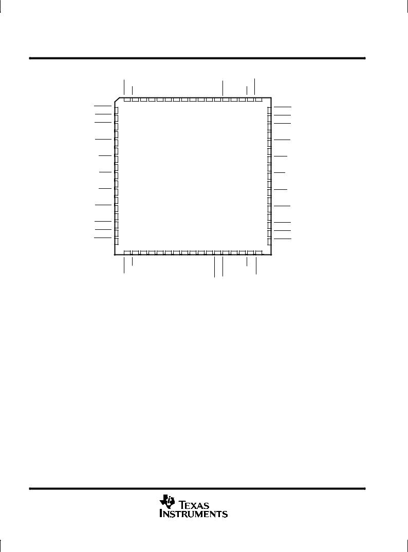
The TL16C554 and the TL16C554I are available in a 68-pin plastic-leaded chip-carrier (PLCC) FN package and in an 80-pin (TQFP) PN package.
Please be aware that an important notice concerning availability, standard warranty, and use in critical applications of Texas Instruments semiconductor products and disclaimers thereto appears at the end of this data sheet.
PRODUCTION DATA information is current as of publication date. Products conform to specifications per the terms of Texas Instruments standard warranty. Production processing does not necessarily include testing of all parameters.
Copyright 1998, Texas Instruments Incorporated
POST OFFICE BOX 655303 •DALLAS, TEXAS 75265 |
1 |
TL16C554, TL16C554I
ASYNCHRONOUS COMMUNICATIONS ELEMENT
SLLS165D ± JANUARY 1994 ± REVISED JULY 1998
|
|
|
|
|
|
|
FN PACKAGE |
|
|
|
|
|
|
|
|||
|
DCDA |
RIA |
RXA |
GND |
D7 |
D6 |
(TOP VIEW) |
D0 |
INTN |
|
RXD |
RID |
DCDD |
|
|||
|
D5 |
D4 |
D3 |
D2 D1 |
V |
|
|||||||||||
|
|
|
|
|
|
|
|
|
|
|
|
|
CC |
|
|
|
|
DSRA |
9 |
8 |
7 |
6 |
5 |
4 |
3 |
2 |
1 |
68 67 66 65 64 63 62 61 |
DSRD |
||||||
10 |
|
|
|
|
|
|
|
|
|
|
|
|
|
|
60 |
||
CTSA |
11 |
|
|
|
|
|
|
|
|
|
|
|
|
|
|
59 |
CTSD |
DTRA |
12 |
|
|
|
|
|
|
|
|
|
|
|
|
|
|
58 |
DTRD |
VCC |
13 |
|
|
|
|
|
|
|
|
|
|
|
|
|
|
57 |
GND |
RTSA |
14 |
|
|
|
|
|
|
|
|
|
|
|
|
|
|
56 |
RTSD |
INTA |
15 |
|
|
|
|
|
|
|
|
|
|
|
|
|
|
55 |
INTD |
CSA |
16 |
|
|
|
|
|
|
|
|
|
|
|
|
|
|
54 |
CSD |
TXA |
17 |
|
|
|
|
|
|
|
|
|
|
|
|
|
|
53 |
TXD |
IOW |
18 |
|
|
|
|
|
|
|
|
|
|
|
|
|
|
52 |
IOR |
TXB |
19 |
|
|
|
|
|
|
|
|
|
|
|
|
|
|
51 |
TXC |
CSB |
20 |
|
|
|
|
|
|
|
|
|
|
|
|
|
|
50 |
CSC |
INTB |
21 |
|
|
|
|
|
|
|
|
|
|
|
|
|
|
49 |
INTC |
RTSB |
22 |
|
|
|
|
|
|
|
|
|
|
|
|
|
|
48 |
RTSC |
GND |
23 |
|
|
|
|
|
|
|
|
|
|
|
|
|
|
47 |
VCC |
DTRB |
24 |
|
|
|
|
|
|
|
|
|
|
|
|
|
|
46 |
DTRC |
CTSB |
25 |
|
|
|
|
|
|
|
|
|
|
|
|
|
|
45 |
CTSC |
DSRB |
26 |
|
|
|
|
|
|
|
|
|
|
|
|
|
|
44 |
DSRC |
|
27 |
28 29 30 31 32 33 34 35 36 37 38 39 40 41 42 43 |
|
||||||||||||||
|
DCDB |
RIB |
RXB |
V |
NC |
A2 |
A1 |
A0 |
XTAL1 |
XTAL2 RESET |
RXRDY |
TXRDY |
GND |
RXC |
RIC |
DCDC |
|
|
|
|
|
CC |
|
|
|
|
|
|
|
|
|
|
|
|
|
NC ± No internal connection |
|
|
|
|
|
|
|
|
|
|
|
|
|||||
2 |
POST OFFICE BOX 655303 •DALLAS, TEXAS 75265 |

TL16C554, TL16C554I
ASYNCHRONOUS COMMUNICATIONS ELEMENT
SLLS165D ± JANUARY 1994 ± REVISED JULY 1998
PN PACKAGE (TOP VIEW)
|
|
|
|
|
|
|
|
|
|
|
|
DCDC |
RIC |
RXC |
GND |
|
TXRDY |
|
RXRDY |
RESET |
NC |
|
XTAL2 XTAL1 NC |
|
|
|
|
|
RXB |
|
RIB |
|
DCDB |
NC |
|
|
|
||||||||||||||||||||||
|
|
|
|
|
|
|
|
|
|
|
NC |
|
|
|
|
A0 A1 |
|
A2 |
|
V |
|
|
|
|
|
||||||||||||||||||||||||||||||||||
|
|
|
|
|
|
|
|
|
|
|
|
|
|
|
|
|
|
|
|
|
|
||||||||||||||||||||||||||||||||||||||
|
|
|
|
|
|
|
|
|
|
|
|
|
|
|
|
|
|
|
|
|
|
|
|
|
|
|
|
|
|
|
|
|
|
|
|
|
|
|
|
|
|
CC |
|
|
|
|
|
|
|
|
|
|
|
|
|
|
|
|
|
|
|
|
|
|
|
|
|
|
|
|
|
|
|
|
|
|
|
|
|
|
|
|
|
|
|
|
|
|
|
|
|
|
|
|
|
|
|
|
|
|
|
|
|
|
|
|
|
|
|
|
|
|
|
|
|
|
|
||
|
|
|
|
|
|
|
|
|
|
|
|
|
|
|
|
|
|
|
|
|
|
|
|
|
|
|
|
|
|
|
|
|
|
|
|
|
|
|
|
|
|
|
|
|
|
|
|
|
|
|
|
|
|
|
|
|
|
|
|
|
|
|
|
|
|
|
|
|
|
|
|
|
|
|
|
|
|
|
|
|
|
|
|
|
|
|
|
|
|
|
|
|
|
|
|
|
|
|
|
|
|
|
|
|
|
|
|
|
|
|
|
|
|
|
|
|
|
|
|
|
|
|
|
|
|
|
|
|
|
|
|
|
|
|
|
|
|
|
|
|
|
|
|
|
|
|
|
|
|
|
|
|
|
|
|
|
|
|
|
|
|
|
|
|
|
|
|
|
|
|
|
|
|
|
|
|
|
|
|
|
|
|
NC |
|
|
|
60 59 58 |
|
57 56 55 54 53 52 51 50 49 48 47 46 45 44 43 42 41 |
|
|
|
|
NC |
|||||||||||||||||||||||||||||||||||||||||||||
|
|
|
|
|
|
||||||||||||||||||||||||||||||||||||||||||||||||||||||
|
|
|
|
|
|
|
61 |
|
|
|
|
|
|
|
|
|
|
|
|
|
|
|
|
|
|
|
|
|
|
|
|
|
|
|
|
|
|
|
|
|
|
|
|
|
|
|
|
|
40 |
|
|
||||||||
|
|
|
|
|
|
|
|
|
|
|
|
|
|
|
|
|
|
|
|
|
|
|
|
|
|
|
|
|
|
|
|
|
|
|
|
|
|
|
|
|
|
|
|
|
|
|
|
|
|
||||||||||
|
|
|
|
|
|
|
|
|
|
|
|
|
|
|
|
|
|
|
|
|
|
|
|
|
|
|
|
|
|
|
|
|
|
|
|
|
|
|
|
|
|
|
|
|
|
|
|
|
|
|
|
|
|
|
|
|
|
|
|
DSRC |
|
|
|
|
62 |
|
|
|
|
|
|
|
|
|
|
|
|
|
|
|
|
|
|
|
|
|
|
|
|
|
|
|
|
|
|
|
|
|
|
|
|
|
|
|
|
|
39 |
|
|
DSRB |
|||||||||
|
|
|
|
|
|
|
|
|
|
|
|
|
|
|
|
|
|
|
|
|
|
|
|
|
|
|
|
|
|
|
|
|
|
|
|
|
|
|
|
|
|
|
|
|
|
|
|
|
|
|
|
|
|
|
|
|
|
|
|
|
CTSC |
|
|
|
|
63 |
|
|
|
|
|
|
|
|
|
|
|
|
|
|
|
|
|
|
|
|
|
|
|
|
|
|
|
|
|
|
|
|
|
|
|
|
|
|
|
|
|
38 |
|
|
CTSB |
|
|||||||
|
|
|
|
|
|
|
|
|
|
|
|
|
|
|
|
|
|
|
|
|
|
|
|
|
|
|
|
|
|
|
|
|
|
|
|
|
|
|
|
|
|
|
|
|
|
|
|
|
|
|
|
|
|
|
|
|
|
|
|
DTRC |
|
|
|
|
64 |
|
|
|
|
|
|
|
|
|
|
|
|
|
|
|
|
|
|
|
|
|
|
|
|
|
|
|
|
|
|
|
|
|
|
|
|
|
|
|
|
|
37 |
|
|
DTRB |
|
||||||||
|
|
VCC |
|
|
|
|
65 |
|
|
|
|
|
|
|
|
|
|
|
|
|
|
|
|
|
|
|
|
|
|
|
|
|
|
|
|
|
|
|
|
|
|
|
|
|
|
|
|
|
36 |
|
|
GND |
|||||||
|
|
|
|
|
|
|
|
|
|
|
|
|
|
|
|
|
|
|
|
|
|
|
|
|
|
|
|
|
|
|
|
|
|
|
|
|
|
|
|
|
|
|
|
|
|
|
|
|
|||||||||||
|
|
|
|
|
|
|
|
|
|
|
|
|
|
|
|
|
|
|
|
|
|
|
|
|
|
|
|
|
|
|
|
|
|
|
|
|
|
|
|
|
|
|
|
|
|
|
|
||||||||||||
|
RTSC |
|
|
|
|
66 |
|
|
|
|
|
|
|
|
|
|
|
|
|
|
|
|
|
|
|
|
|
|
|
|
|
|
|
|
|
|
|
|
|
|
|
|
|
|
|
|
|
35 |
|
|
RTSB |
|
|||||||
|
INTC |
|
|
|
|
67 |
|
|
|
|
|
|
|
|
|
|
|
|
|
|
|
|
|
|
|
|
|
|
|
|
|
|
|
|
|
|
|
|
|
|
|
|
|
|
|
|
|
34 |
|
|
INTB |
||||||||
|
|
|
|
|
|
|
|
|
|
|
|
|
|
|
|
|
|
|
|
|
|
|
|
|
|
|
|
|
|
|
|
|
|
|
|
|
|
|
|
|
|
|
|
|
|
|
|
||||||||||||
|
|
|
|
|
|
|
|
|
|
|
|
|
|
|
|
|
|
|
|
|
|
|
|
|
|
|
|
|
|
|
|
|
|
|
|
|
|
|
|
|
|
|
|
|
|
|
|
|
|
|
|
|
|
|
|
|
|
|
|
|
|
CSC |
|
|
|
|
68 |
|
|
|
|
|
|
|
|
|
|
|
|
|
|
|
|
|
|
|
|
|
|
|
|
|
|
|
|
|
|
|
|
|
|
|
|
|
|
|
|
|
33 |
|
|
CSB |
|
|
|||||
|
|
TXC |
|
|
|
|
69 |
|
|
|
|
|
|
|
|
|
|
|
|
|
|
|
|
|
|
|
|
|
|
|
|
|
|
|
|
|
|
|
|
|
|
|
|
|
|
|
|
|
32 |
|
|
TXB |
|||||||
|
|
|
|
|
|
|
|
|
|
|
|
|
|
|
|
|
|
|
|
|
|
|
|
|
|
|
|
|
|
|
|
|
|
|
|
|
|
|
|
|
|
|
|
|
|
|
|
|
|||||||||||
|
|
|
|
|
|
|
|
|
|
|
|
|
|
|
|
|
|
|
|
|
|
|
|
|
|
|
|
|
|
|
|
|
|
|
|
|
|
|
|
|
|
|
|
|
|
|
|
|
|
|
|
|
|
|
|
|
|
|
|
|
|
|
IOR |
|
|
|
|
70 |
|
|
|
|
|
|
|
|
|
|
|
|
|
|
|
|
|
|
|
|
|
|
|
|
|
|
|
|
|
|
|
|
|
|
|
|
|
|
|
|
|
31 |
|
|
IOW |
|
|
||||
|
|
|
NC |
|
|
|
|
71 |
|
|
|
|
|
|
|
|
|
|
|
|
|
|
|
|
|
|
|
|
|
|
|
|
|
|
|
|
|
|
|
|
|
|
|
|
|
|
|
|
|
30 |
|
|
NC |
||||||
|
|
|
|
|
|
|
|
|
|
|
|
|
|
|
|
|
|
|
|
|
|
|
|
|
|
|
|
|
|
|
|
|
|
|
|
|
|
|
|
|
|
|
|
|
|
|
|
|
|
||||||||||
|
|
TXD |
|
|
|
|
72 |
|
|
|
|
|
|
|
|
|
|
|
|
|
|
|
|
|
|
|
|
|
|
|
|
|
|
|
|
|
|
|
|
|
|
|
|
|
|
|
|
|
29 |
|
|
TXA |
|||||||
|
|
|
|
|
|
|
|
|
|
|
|
|
|
|
|
|
|
|
|
|
|
|
|
|
|
|
|
|
|
|
|
|
|
|
|
|
|
|
|
|
|
|
|
|
|
|
|
|
|||||||||||
|
|
|
|
|
|
|
|
|
|
|
|
|
|
|
|
|
|
|
|
|
|
|
|
|
|
|
|
|
|
|
|
|
|
|
|
|
|
|
|
|
|
|
|
|
|
|
|
|
|
|
|
|
|
|
|
|
|
|
|
|
|
CSD |
|
|
|
|
73 |
|
|
|
|
|
|
|
|
|
|
|
|
|
|
|
|
|
|
|
|
|
|
|
|
|
|
|
|
|
|
|
|
|
|
|
|
|
|
|
|
|
28 |
|
|
CSA |
|
|
|||||
|
INTD |
|
|
|
|
74 |
|
|
|
|
|
|
|
|
|
|
|
|
|
|
|
|
|
|
|
|
|
|
|
|
|
|
|
|
|
|
|
|
|
|
|
|
|
|
|
|
|
27 |
|
|
INTA |
||||||||
|
|
|
|
|
|
|
|
|
|
|
|
|
|
|
|
|
|
|
|
|
|
|
|
|
|
|
|
|
|
|
|
|
|
|
|
|
|
|
|
|
|
|
|
|
|
|
|||||||||||||
|
|
|
|
|
|
|
|
|
|
|
|
|
|
|
|
|
|
|
|
|
|
|
|
|
|
|
|
|
|
|
|
|
|
|
|
|
|
|
|
|
|
|
|
|
|
|
|
|
|
|
|
|
|
|
|
|
|
|
|
|
RTSD |
|
|
|
75 |
|
|
|
|
|
|
|
|
|
|
|
|
|
|
|
|
|
|
|
|
|
|
|
|
|
|
|
|
|
|
|
|
|
|
|
|
|
|
|
|
|
26 |
|
|
RTSA |
|
||||||||
|
GND |
|
|
|
|
76 |
|
|
|
|
|
|
|
|
|
|
|
|
|
|
|
|
|
|
|
|
|
|
|
|
|
|
|
|
|
|
|
|
|
|
|
|
|
|
|
|
|
25 |
|
|
VCC |
||||||||
|
|
|
|
|
|
|
|
|
|
|
|
|
|
|
|
|
|
|
|
|
|
|
|
|
|
|
|
|
|
|
|
|
|
|
|
|
|
|
|
|
|
|
|
|
|
|
|
||||||||||||
|
|
|
|
|
|
|
|
|
|
|
|
|
|
|
|
|
|
|
|
|
|
|
|
|
|
|
|
|
|
|
|
|
|
|
|
|
|
|
|
|
|
|
|
|
|
|
|
||||||||||||
DTRD |
|
|
|
77 |
|
|
|
|
|
|
|
|
|
|
|
|
|
|
|
|
|
|
|
|
|
|
|
|
|
|
|
|
|
|
|
|
|
|
|
|
|
|
|
|
|
24 |
|
|
DTRA |
|
|||||||||
|
|
|
|
|
|
|
|
|
|
|
|
|
|
|
|
|
|
|
|
|
|
|
|
|
|
|
|
|
|
|
|
|
|
|
|
|
|
|
|
|
|
|
|
|
|
|
|
|
|
|
|
|
|
|
|
|
|
|
|
|
CTSD |
|
|
|
78 |
|
|
|
|
|
|
|
|
|
|
|
|
|
|
|
|
|
|
|
|
|
|
|
|
|
|
|
|
|
|
|
|
|
|
|
|
|
|
|
|
|
23 |
|
|
CTSA |
|
||||||||
|
|
|
|
|
|
|
|
|
|
|
|
|
|
|
|
|
|
|
|
|
|
|
|
|
|
|
|
|
|
|
|
|
|
|
|
|
|
|
|
|
|
|
|
|
|
|
|
|
|
|
|
|
|
|
|
|
|
|
|
DSRD |
|
|
|
|
79 |
|
|
|
|
|
|
|
|
|
|
|
|
|
|
|
|
|
|
|
|
|
|
|
|
|
|
|
|
|
|
|
|
|
|
|
|
|
|
|
|
|
22 |
|
|
DSRA |
|||||||||
|
|
|
NC |
|
|
|
|
80 |
|
|
|
|
|
|
|
|
|
|
|
|
|
|
|
|
|
|
|
|
|
|
|
|
|
|
|
|
|
|
|
|
|
|
|
|
|
|
|
|
|
21 |
|
|
NC |
||||||
|
|
|
|
|
|
|
|
|
|
|
|
|
|
|
|
|
|
|
|
|
|
|
|
|
|
|
|
|
|
|
|
|
|
|
|
|
|
|
|
|
|
|
|
|
|
|
|
|
|
||||||||||
|
|
|
|
|
|
|
1 |
|
|
2 |
|
3 |
|
4 |
|
5 |
6 |
7 |
|
8 |
|
9 |
10 11 12 13 14 15 16 17 18 19 |
|
20 |
|
|
|
|
|
|
||||||||||||||||||||||||||||
|
|
|
|
|
|
|
|
|
|
|
|
|
|
|
|
|
|
||||||||||||||||||||||||||||||||||||||||||
|
|
|
|
|
|
|
|
|
|
|
|
|
|
|
|
|
|
|
|
|
|
|
|
|
|
|
|
|
|
|
|
|
|
|
|
|
|
|
|
|
|
|
|
|
|
|
|
|
|
|
|
|
|
|
|
|
|
||
|
|
|
|
|
|
|
|
|
|
|
|
|
|
|
|
|
|
|
D0 |
D1 |
D2 |
|
NC D3 D4 |
D5 D6 |
|
D7 |
|
|
|
|
|
|
|
|
|
|
|||||||||||||||||||||||
|
|
|
|
|
|
|
|
|
|
|
NC |
DCDD |
RID |
RXD |
V |
|
INTN |
|
|
|
|
GND |
RXA |
|
|
RIA |
|
DCDA |
NC |
|
|
|
|||||||||||||||||||||||||||
|
|
|
|
|
|
|
|
|
|
|
|
|
|
|
|
|
|
|
|
CC |
|
|
|
|
|
|
|
|
|
|
|
|
|
|
|
|
|
|
|
|
|
|
|
|
|
|
|
|
|
|
|
|
|
|
|
|
|
|
|
|
|
|
|
|
|
|
|
|
|
|
|
|
|
|
|
|
|
|
|
|
|
|
|
|
|
|
|
|
|
|
|
|
|
|
|
|
|
|
|
|
|
|
|
|
|
|
|
|
|
|
|
|
|
|
|
|
|
|
|
|
|
|
|
|
|
|
|
|
|
|
|
|
|
|
|
|
|
|
|
|
|
|
|
|
|
|
|
|
|
|
|
|
|
|
|
|
|
|
|
|
|
|
|
|
|
|
|
|
|
|
|
|
|
|
|
|
|
|
|
|
|
|
|
|
|
|
|
|
|
|
|
|
|
|
|
|
|
|
|
|
|
|
|
|
|
|
|
|
|
|
|
|
|
|
|
|
|
|
|
|
|
|
|
|
|
|
|
|
|
|
|
|
|
|
|
|
|
|
|
NC ± No internal connection
POST OFFICE BOX 655303 •DALLAS, TEXAS 75265 |
3 |
TL16C554, TL16C554I |
|
|
|
||
ASYNCHRONOUS COMMUNICATIONS ELEMENT |
|
|
|||
SLLS165D ± JANUARY 1994 ± REVISED JULY 1998 |
|
|
|||
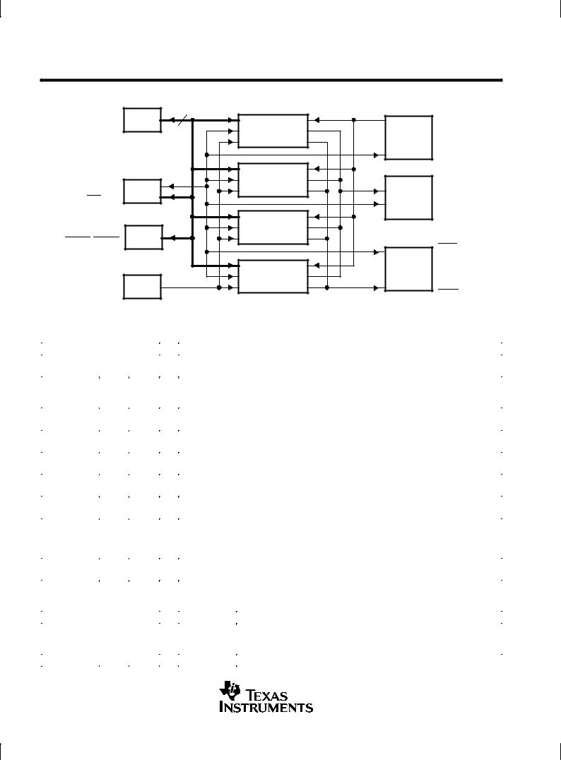
functional block diagram² |
|
|
|
||
D7 ± D0 |
Data |
8 |
|
|
|
Bus |
TL16C550B |
|
|
||
|
Receive |
|
|||
|
|
|
|||
|
|
Circuitry |
Control |
RXx |
|
|
|
|
Logic |
|
|
A2 ± A0 |
|
TL16C550B |
|
|
|
Control |
Circuitry |
Transmit |
|
||
CSx |
|
||||
|
|
||||
Logic |
|
Control |
TXx |
||
IOR, IOW |
|
||||
|
|
Logic |
|
||
RESET |
|
|
|
||
|
|
|
|
||
|
Interrupt |
TL16C550B |
|
|
|
INTx |
Circuitry |
|
|
||
TXRDY, RXRDY |
Logic |
|
|
CTSx |
|
|
|
|
|
||
|
|
|
Modem |
RTSx |
|
|
|
|
DSRx |
||
|
|
TL16C550B |
Control |
||
|
|
DTRx |
|||
|
|
Logic |
|||
XTAL1 |
Clock |
Circuitry |
|||
|
RIx |
||||
XTAL2 |
Circuit |
|
|
||
|
|
DCDx |
|||
|
|
|
|
||
² For TL16C550 circuitry, refer to the TL16C550B data sheet.
|
|
|
|
|
|
|
|
|
|
|
|
|
|
|
|
|
|
|
|
|
|
|
Terminal Functions |
|
||||||||||||
|
|
|
|
|
|
|
|
|
|
|
|
|
|
|
|
|
|
|
|
|
|
|
|
|
|
|
|
|
|
|
|
|
|
|
|
|
|
|
|
|
|
|
|
|
|
|
|
|
|
TERMINAL |
|
|
|
|
|
|
|
|
|
|
|
|
|
|
|
|
|
|
|||||
|
NAME |
FN |
PN |
I/O |
|
|
|
|
|
|
|
|
|
|
|
|
|
|
DESCRIPTION |
|
||||||||||||||||
|
NO. |
NO. |
|
|
|
|
|
|
|
|
|
|
|
|
|
|
|
|
|
|||||||||||||||||
|
|
|
|
|
|
|
|
|
|
|
|
|
|
|
|
|
|
|
|
|
|
|
|
|
|
|
|
|
|
|
|
|
|
|
||
|
|
|
|
|
|
|
|
|
|
|
|
|
|
|
|
|
|
|
|
|
|
|
|
|
|
|
|
|
|
|
|
|
|
|
|
|
|
A0 |
34 |
48 |
I |
Register select terminals. A0, A1, and A2 are three inputs used during read and write operations to |
|
||||||||||||||||||||||||||||||
|
A1 |
33 |
47 |
|
select the ACE register to read or write. |
|
||||||||||||||||||||||||||||||
|
A2 |
32 |
46 |
|
|
|
|
|
|
|
|
|
|
|
|
|
|
|
|
|
||||||||||||||||
|
|
|
|
|
|
|
|
|
|
|
|
|
|
|
|
|
|
|
|
|
|
|
|
|
|
|
|
|
|
|
|
|
|
|
||
|
|
, |
|
|
|
|
|
|
|
|
|
, |
|
|
|
|
16, 20, |
28, 33, |
I |
Chip select. Each chip select |
|
enables read and write operations to its respective channel. |
|
|||||||||||||
|
CSA |
CSB |
|
|
|
|
(CSx) |
|
||||||||||||||||||||||||||||
|
CSC, CSD |
50, 54 |
68, 73 |
|
|
|
|
|
|
|
|
|
|
|
|
|
|
|
|
|
||||||||||||||||
|
|
|
|
|
|
|
|
|
|
|
|
|
|
|
|
|
|
|
|
|
|
|
|
|
|
|
|
|
|
|||||||
|
|
|
|
|
, |
|
|
|
|
|
, |
|
11, 25, |
23, 38, |
I |
Clear to send. |
|
|
|
|
is a modem status signal. Its condition can be checked by reading bit 4 (CTS) |
|
||||||||||||||
|
CTSA |
CTSB |
|
CTSx |
|
|
||||||||||||||||||||||||||||||
|
CTSC, CTSD |
45, 59 |
63, 78 |
|
of the modem status register. CTS has no affect on the transmit or receive operation. |
|
||||||||||||||||||||||||||||||
|
|
|
|
|
|
|
|
|
|
|
|
|
|
|
|
|
|
|
|
|
|
|
|
|
|
|||||||||||
|
D7 ± D0 |
66± 68 |
15±11, |
I/O |
Data bus. Eight data lines with 3-state outputs provide a bidirectional path for data, control, and status |
|
||||||||||||||||||||||||||||||
|
|
|
|
|
|
|
|
|
|
|
|
|
|
|
|
|
|
1 ± 5 |
9±7 |
|
information between the TL16C554 and the CPU. D0 is the least significant bit (LSB). |
|
||||||||||||||
|
|
|
|
|
|
|
|
|
|
|
|
|
|
|
|
|
|
|
|
|
|
|
|
|
||||||||||||
|
|
|
|
|
|
|
|
, |
|
|
|
|
|
|
|
, |
9, 27, |
19,42, |
I |
Data carrier detect. A low on |
|
|
|
indicates the carrier has been detected by the modem. The |
|
|||||||||||
|
DCDA |
|
|
DCDB |
DCDx |
|
||||||||||||||||||||||||||||||
|
DCDC, DCDD |
43, 61 |
59, 2 |
|
condition of this signal is checked by reading bit 7 of the modem status register. |
|
||||||||||||||||||||||||||||||
|
|
|
|
|
|
|
|
|
|
|
|
|
|
|
|
|
|
|
|
|||||||||||||||||
|
|
|
|
|
|
|
, |
|
|
|
|
|
|
, |
10, 26, |
22, 39, |
|
Data set ready. |
|
|
|
|
is a modem status signal. Its condition can be checked by reading bit 5 (DSR) |
|
||||||||||||
|
DSRA |
|
DSRB |
I |
DSRx |
|
||||||||||||||||||||||||||||||
DSRC, DSRD |
44, 60 |
62, 79 |
of the modem status register. DSR has no affect on the transmit or receive operation. |
|
||||||||||||||||||||||||||||||||
|
|
|||||||||||||||||||||||||||||||||||
|
|
|
|
|
|
|
|
|
|
|
|
|
|
|
|
|||||||||||||||||||||
|
|
|
|
|
|
, |
|
|
|
|
|
, |
12, 24, |
24, 37, |
O |
Data terminal ready. |
|
|
|
is an output that indicates to a modem or data set that the ACE is ready |
|
|||||||||||||||
|
DTRA |
DTRB |
DTRx |
|
||||||||||||||||||||||||||||||||
|
DTRC, DTRD |
46, 58 |
64, 77 |
|
to establish communications. It is placed in the active state by setting the DTR bit of the modem |
|
||||||||||||||||||||||||||||||
|
|
|
|
|
|
|
|
|
|
|
|
|
|
|
|
|
|
|
|
|
control register. DTRx is placed in the inactive state (high) either as a result of the master reset during |
|
||||||||||||||
|
|
|
|
|
|
|
|
|
|
|
|
|
|
|
|
|
|
|
|
|
loop mode operation or clearing bit 0 (DTR) of the modem control register. |
|
||||||||||||||
|
|
|
|
|
|
|
|
|
|
|
|
|||||||||||||||||||||||||
|
GND |
6, 23, |
16, 36, |
|
Signal and power ground |
|
||||||||||||||||||||||||||||||
|
|
|
|
|
|
|
|
|
|
|
|
|
|
|
|
|
|
40, 57 |
56, 76 |
|
|
|
|
|
|
|
|
|
|
|
|
|
|
|
|
|
|
|
|
|
|
|
|
|
|
|
|
|
|||||||||||||||||||||||||
|
|
|
|
65 |
6 |
I |
|
|
|
|
|
|||||||||||||||||||||||||
|
INTN |
|
Interrupt normal. |
INTN |
operates in conjunction with bit 3 of the modem status register and affects |
|
||||||||||||||||||||||||||||||
|
|
|
|
|
|
|
|
|
|
|
|
|
|
|
|
|
|
|
|
|
operation of the interrupts (INTA, INTB, INTC, and INTD) for the four universal asynchronous |
|
||||||||||||||
|
|
|
|
|
|
|
|
|
|
|
|
|
|
|
|
|
|
|
|
|
receiver/transceivers (UARTs) per the following table. |
|
||||||||||||||
|
|
|
|
|
|
|
|
|
|
|
|
|
|
|
|
|
|
|
|
|
|
|
|
|
|
|
|
|
|
|
|
|
|
|
||
|
|
|
|
|
|
|
|
|
|
|
|
|
|
|
|
|
|
|
|
|
|
INTN |
|
|
|
|
|
|
|
|
|
|
|
OPERATION OF INTERRUPTS |
|
|
|
|
|
|
|
|
|
|
|
|
|
|
|
|
|
|
|
|
|
|
|
|
|
|
|
||||||||||||
|
|
|
|
|
|
|
|
|
|
|
|
|
|
|
|
|
|
|
|
|
Brought low or |
|
Interrupts are enabled according to the state of OUT2 (MCR bit 3). When the MCR |
|
||||||||||||
|
|
|
|
|
|
|
|
|
|
|
|
|
|
|
|
|
|
|
|
|
allowed to float |
|
bit 3 is cleared, the 3-state interrupt output of that UART is in the high-impedance |
|
||||||||||||
|
|
|
|
|
|
|
|
|
|
|
|
|
|
|
|
|
|
|
|
|
|
|
|
|
|
state. When the MCR bit 3 is set, the interrupt output of the UART is enabled. |
|
|||||||||
|
|
|
|
|
|
|
|
|
|
|
|
|
|
|
|
|
|
|
|
|
|
|
|
|
||||||||||||
|
|
|
|
|
|
|
|
|
|
|
|
|
|
|
|
|
|
|
|
|
Brought high |
|
Interrupts are always enabled, overriding the OUT2 enables. |
|
||||||||||||
|
|
|
|
|
|
|
|
|
|
|
|
|
|
|
|
|
|
|
|
|
|
|
|
|
|
|
|
|
|
|
|
|
|
|
|
|
|
|
|
|
|
|
|
|
|
|
|
|
|
|
|
|
|
|
|
|
|
|
|
|
|
|
|
|
|
|
|
|
|
|
|
|
|
4 |
POST OFFICE BOX 655303 •DALLAS, TEXAS 75265 |

|
|
|
|
|
|
|
|
|
|
|
|
|
|
|
|
|
|
|
|
|
|
|
|
|
|
|
|
|
TL16C554, TL16C554I |
|
|
|
|
|
|
|
|
|
|
|
|
|
|
|
|
|
|
|
|
|
ASYNCHRONOUS COMMUNICATIONS ELEMENT |
||||||||||
|
|
|
|
|
|
|
|
|
|
|
|
|
|
|
|
|
|
|
|
|
|
|
|
|
|
|
|
SLLS165D ± JANUARY 1994 ± REVISED JULY 1998 |
||
|
|
|
|
|
|
|
|
|
|
|
|
|
|
|
|
|
|
|
|
|
|
|
|
|
|
|
|
|
|
|
|
|
|
|
|
|
|
|
|
|
|
|
|
|
|
|
Terminal Functions (Continued) |
|
|
||||||||||||
|
|
|
|
|
|
|
|
|
|
|
|
|
|
|
|
|
|
|
|
|
|
|
|
|
|
|
|
|
|
|
|
|
|
|
|
|
|
|
|
|
TERMINAL |
|
|
|
|
|
|
|
|
|
|
|
|
|
|
|
|
|
|
||
|
|
|
NAME |
FN |
PN |
I/O |
|
|
|
|
|
|
|
|
|
|
|
|
|
DESCRIPTION |
|
|
||||||||
|
|
|
NO. |
NO. |
|
|
|
|
|
|
|
|
|
|
|
|
|
|
|
|
|
|||||||||
|
|
|
|
|
|
|
|
|
|
|
|
|
|
|
|
|
|
|
|
|
|
|
|
|
|
|
|
|
||
|
|
|
|
|
|
|
|
|
|
|
|
|
|
|
|
|
|
|
|
|
|
|
|
|
|
|
|
|
|
|
|
INTA, INTB, |
15, 21, |
27, 34, |
O |
|
External interrupt output. The INTx outputs go high (when enabled by the interrupt register) and |
|
|||||||||||||||||||||||
|
INTC, INTD |
49, 55 |
67, 74 |
|
|
inform the CPU that the ACE has an interrupt to be serviced. Four conditions that cause an interrupt |
|
|||||||||||||||||||||||
|
|
|
|
|
|
|
|
|
|
|
|
|
|
|
|
to be issued are: a receiver error, receiver data available or timeout (FIFO mode only), transmitter |
|
|||||||||||||
|
|
|
|
|
|
|
|
|
|
|
|
|
|
|
|
holding register empty, and an enabled modem status interrupt. The interrupt is disabled when it is |
|
|||||||||||||
|
|
|
|
|
|
|
|
|
|
|
|
|
|
|
|
serviced or as the result of a master reset. |
|
|
||||||||||||
|
|
|
|
|
|
|
|
|
|
|
|
|
|
|
|
|
|
|
|
|
|
|
|
|
|
|
|
|
||
|
|
|
|
|
|
|
|
|
|
|
|
52 |
70 |
I |
|
Read strobe. A low level on |
|
|
|
transfers the contents of the TL16C554 data bus to the external CPU |
|
|||||||||
|
IOR |
|
|
|
|
|
|
|
|
|
|
IOR |
|
|||||||||||||||||
|
|
|
|
|
|
|
|
|
|
|
|
|
|
|
|
bus. |
|
|
||||||||||||
|
|
|
|
|
|
|
|
|
|
|
|
|
|
|
|
|
|
|
|
|
|
|
|
|
|
|||||
|
|
|
|
|
|
|
|
|
|
|
|
18 |
31 |
I |
|
Write strobe. |
|
|
|
allows the CPU to write into the selected address by the address register. |
|
|||||||||
|
IOW |
|
|
|
|
|
|
|
|
|
IOW |
|
||||||||||||||||||
|
|
|
|
|
|
|
|
|
|
|
|
|
|
|
|
|
|
|
|
|
|
|
|
|||||||
|
RESET |
37 |
53 |
I |
|
Master reset. When active, RESET clears most ACE registers and sets the state of various signals. |
|
|||||||||||||||||||||||
|
|
|
|
|
|
|
|
|
|
|
|
|
|
|
|
The transmitter output and the receiver input is disabled during reset time. |
|
|||||||||||||
|
|
|
|
|
|
|
|
|
|
|
|
|
|
|
|
|
|
|
|
|
|
|
||||||||
|
|
, |
|
|
|
|
|
, |
|
8, 28, |
18, 43, |
I |
|
Ring detect indicator. A low on |
|
|
|
indicates the modem has received a ring signal from the telephone |
|
|||||||||||
|
RIA |
RIB |
|
|
RIx |
|
||||||||||||||||||||||||
|
RIC, RID |
42, 62 |
58, 3 |
|
|
line. The condition of this signal can be checked by reading bit 6 of the modem status register. |
|
|||||||||||||||||||||||
|
|
|
|
|
|
|
|
|
|
|
|
|
|
|
|
|
|
|||||||||||||
|
|
|
|
|
|
, |
|
|
|
|
, |
14, 22, |
26, 35, |
O |
|
Request to send. When active, |
|
|
|
informs the modem or data set that the ACE is ready to receive |
|
|||||||||
|
RTSA |
RTSB |
|
RTSx |
|
|||||||||||||||||||||||||
|
RTSC, RTSD |
48, 56 |
66, 75 |
|
|
data. Writing a 1 in the modem control register sets this bit to a low state. After reset, this terminal |
|
|||||||||||||||||||||||
|
|
|
|
|
|
|
|
|
|
|
|
|
|
|
|
is set high. These terminals have no affect on the transmit or receive operation. |
|
|||||||||||||
|
|
|
|
|
|
|
|
|
|
|
|
|
|
|||||||||||||||||
|
RXA, RXB |
7, 29, |
17, 44, |
I |
|
Serial input. RXx is a serial data input from a connected communications device. During loopback |
|
|||||||||||||||||||||||
|
RXC, RXD |
41, 63 |
57, 4 |
|
|
mode, the RXx input is disabled from external connection and connected to the TXx output internally. |
|
|||||||||||||||||||||||
|
|
|
|
|
|
|
|
|
|
|
|
|
||||||||||||||||||
|
|
|
|
|
|
|
|
|
|
|
|
38 |
54 |
O |
|
Receive ready. |
|
|
|
|
goes low when the receive FIFO is full. It can be used as a single transfer |
|
||||||||
|
RXRDY |
|
|
RXRDY |
|
|
||||||||||||||||||||||||
|
|
|
|
|
|
|
|
|
|
|
|
|
|
|
|
or multitransfer. |
|
|
||||||||||||
|
|
|
|
|
|
|
|
|
|
|
||||||||||||||||||||
|
TXA, TXB |
17, 19, |
29, 32, |
O |
|
Transmit outputs. TXx is a composite serial data output that is connected to a communications |
|
|||||||||||||||||||||||
|
TXC, TXD |
51, 53 |
69, 72 |
|
|
device. TXA, TXB, TXC, and TXD are set to the marking (high) state as a result of reset. |
|
|||||||||||||||||||||||
|
|
|
|
|
|
|
|
|
|
|||||||||||||||||||||
|
|
|
|
|
|
|
|
|
|
|
|
39 |
55 |
O |
|
Transmit ready. |
|
|
|
goes low when the transmit FIFO is full. It can be used as a single transfer |
|
|||||||||
|
TXRDY |
|
|
TXRDY |
|
|||||||||||||||||||||||||
|
|
|
|
|
|
|
|
|
|
|
|
|
|
|
|
or multitransfer function. |
|
|
||||||||||||
|
|
|
|
|
|
|
|
|
||||||||||||||||||||||
|
VCC |
13, 30, |
5, 25, |
|
|
Power supply |
|
|
||||||||||||||||||||||
|
|
|
|
|
|
|
|
|
|
|
|
47, 64 |
45, 65 |
|
|
|
|
|
|
|
|
|
|
|
|
|
|
|
|
|
|
|
|
|
|
|
|
|
|||||||||||||||||||||||
|
XTAL1 |
35 |
50 |
I |
|
Crystal input 1 or external clock input. A crystal can be connected to XTAL1 and XTAL2 to utilize the |
|
|||||||||||||||||||||||
|
|
|
|
|
|
|
|
|
|
|
|
|
|
|
|
internal oscillator circuit. An external clock can be connected to drive the internal clock circuits. |
|
|||||||||||||
|
|
|
|
|
|
|
|
|
||||||||||||||||||||||
|
XTAL2 |
36 |
51 |
O |
|
Crystal output 2 or buffered clock output (see XTAL1). |
|
|
||||||||||||||||||||||
absolute maximum ratings over free-air temperature range (unless otherwise noted)² |
||||||||||||||||||||||||||||||
|
|
|
|
|
Supply voltage range, VCC (see Note 1) . . . . . . . . . . . . . . . . . . . . . . . . . . . . . . . . . . . |
. . . . . . . . . . . ±0.5 V to 7 V |
||||||||||||||||||||||||
|
|
|
|
|
Input voltage range at any input, VI . . . . . . . . . . . . . . . . . . . . . . . . . . . . . . . . . . . . . . . . |
. . . . . . . . . . . ±0.5 V to 7 V |
||||||||||||||||||||||||
|
|
|
|
|
Output voltage range, VO . |
. |
. . . . . . . . . . |
. |
. |
. |
. . . . |
|
. . |
. . |
. |
|
. . |
. . |
. . . . . . . . . . . . . . . . . . . . |
. . . . . ±0.5 V to VCC + 3 V |
||||||||||
|
|
|
|
|
Continuous total power dissipation at (or below) 70°C . . . . . . . . . . . . . . . . . . . . . . . . |
. . . . . . . . . . . . . . . 500 mW |
||||||||||||||||||||||||
|
|
|
|
|
Operating free-air temperature range, TA: TL16C554 . . . . . . . . . . . . . . . . . . . . . . . . |
. . . . . . . . . . ±0°C to 70°C |
||||||||||||||||||||||||
|
|
|
|
|
|
|
|
|
|
|
|
|
|
|
|
|
|
|
TL16C554I . . . . . . . . . . . . . . . . . . . . . . . |
. . . . . . . . . ±40°C to 85°C |
||||||||||
. . . . . . . . . . . . . . . . . . . . . . . . . . . . . . . . . . . . . . . . . . . . . . . . . . . ±65°C to 150°C
²Stresses beyond those listed under ªabsolute maximum ratingsº may cause permanent damage to the device. These are stress ratings only, and functional operation of the device at these or any other conditions beyond those indicated under ªrecommended operating conditionsº is not implied. Exposure to absolute-maximum-rated conditions for extended periods may affect device reliability.
NOTE 1: All voltage levels are with respect to GND.
POST OFFICE BOX 655303 •DALLAS, TEXAS 75265 |
5 |
TL16C554, TL16C554I
ASYNCHRONOUS COMMUNICATIONS ELEMENT
SLLS165D ± JANUARY 1994 ± REVISED JULY 1998
recommended operating conditions
|
|
MIN |
NOM |
MAX |
UNIT |
|
|
|
|
|
|
Supply voltage, VCC |
4.75 |
5 |
5.25 |
V |
|
Clock high-level input voltage at XTAL1, VIH(CLK) |
2 |
|
VCC |
V |
|
Clock low-level input voltage at XTAL1, VIL(CLK) |
± 0.5 |
|
0.8 |
V |
|
High-level input voltage, VIH |
2 |
|
VCC |
V |
|
Low-level input voltage, VIL |
± 0.5 |
|
0.8 |
V |
|
Clock frequency, fclock |
|
|
16 |
MHz |
|
Operating free-air temperature, TA |
TL16C554 |
0 |
|
70 |
°C |
|
|
|
|
|
|
TL16C554I |
±40 |
|
85 |
°C |
|
|
|
||||
|
|
|
|
|
|
electrical characteristics over recommended ranges of operating free-air temperature and supply voltage (unless otherwise noted)
|
PARAMETER |
|
|
|
|
|
|
|
TEST CONDITIONS |
MIN TYP² |
MAX |
UNIT |
||
VOH³ |
High-level output voltage |
|
IOH = ± 1 mA |
|
|
2.4 |
|
V |
||||||
VOL³ |
Low-level output voltage |
|
IOL = 1.6 mA |
|
|
|
0.4 |
V |
||||||
IIkg |
Input leakage current |
|
VCC = 5.25 V, |
GND = 0, |
|
|
± 10 |
μA |
||||||
|
VI = 0 to 5.25 V, |
All other terminals floating |
|
|||||||||||
|
|
|
|
|
|
|
|
|||||||
IOZ |
High-impedance output |
|
VCC = 5.25 V, |
GND = 0, VO = 0 to 5.25 V, |
|
± 20 |
μA |
|||||||
current |
|
|
|
Chip selected in write mode or chip deselected |
|
|||||||||
|
|
|
|
|
|
|
||||||||
|
|
|
|
|
|
|
|
|
|
|
|
|||
|
|
|
|
|
VCC |
= 5.25 V, |
TA = 25°C, |
|
|
|
|
|||
|
|
|
|
|
RX, |
|
|
|
|
|
|
|
|
|
ICC |
Supply current |
|
|
DSR, DCD, CTS, and RI at 2 V, |
|
|
50 |
mA |
||||||
|
|
All other inputs at 0.8 V, XTAL1 at 4 MHz, |
|
|||||||||||
|
|
|
|
|
|
|
|
|||||||
|
|
|
|
|
No load on outputs, |
Baud rate = 50 kilobits per second |
|
|
|
|||||
|
|
|
|
|
|
|
|
|
|
|
|
|
||
Ci(XTAL1) |
Clock input capacitance |
|
VCC = 0, |
VSS = 0, |
|
15 |
20 |
pF |
||||||
Co(XTAL2) |
Clock output capacitance |
|
|
20 |
30 |
pF |
||||||||
|
|
|
|
|
All other terminals grounded, |
f = 1 MHz, |
|
|
|
|||||
Ci |
Input capacitance |
|
6 |
10 |
pF |
|||||||||
|
T = 25°C |
|
|
|||||||||||
|
|
|
|
|
A |
|
|
|
|
|
||||
Co |
Output capacitance |
|
|
|
|
|
|
|
|
10 |
20 |
pF |
||
² All typical values are at V |
CC |
= 5 V, T |
= 25°C. |
|
|
|
|
|
||||||
|
|
A |
|
|
|
|
|
|
|
|
|
|
|
|
³ These parameters apply for all outputs except XTAL2.
clock timing requirements over recommended ranges of operating free-air temperature and supply voltage (see Figure 1)
|
|
MIN MAX |
UNIT |
|
|
|
|
tw1 |
Pulse duration, clock high (external clock) |
31 |
ns |
tw2 |
Pulse duration, clock low (external clock) |
31 |
ns |
tw3 |
Pulse duration, RESET |
1000 |
ns |
6 |
POST OFFICE BOX 655303 •DALLAS, TEXAS 75265 |

TL16C554, TL16C554I
ASYNCHRONOUS COMMUNICATIONS ELEMENT
SLLS165D ± JANUARY 1994 ± REVISED JULY 1998
read cycle timing requirements over recommended ranges of operating free-air temperature and supply voltage (see Figure 4)
|
|
|
|
|
|
|
|
|
|
|
|
|
|
|
|
|
|
|
|
|
|
MIN MAX |
UNIT |
|
|
|
|
|
|
|
|
|
|
|
|
|
|
|
|
|
|
|
|
|
|
|
|
|
|
|
|
|
|
|
|
|
|
|
|
|
|
|
|
|
|
|
|
|
|
||
tw4 |
Pulse duration, |
IOR |
low |
75 |
ns |
||||||||||||||||||
tsu1 |
Setup time, |
|
|
|
|
valid before |
|
|
|
|
|
low (see Note 2) |
10 |
ns |
|||||||||
CSx |
IOR |
||||||||||||||||||||||
tsu2 |
Setup time, A2 ± A0 valid before |
|
|
|
|
low (see Note 2) |
15 |
ns |
|||||||||||||||
IOR |
|||||||||||||||||||||||
th1 |
Hold time, A2 ± A0 valid after |
|
|
|
|
|
high (see Note 2) |
0 |
ns |
||||||||||||||
IOR |
|||||||||||||||||||||||
th2 |
Hold time, |
|
|
|
valid after |
|
|
|
|
high (see Note 2) |
0 |
ns |
|||||||||||
CSx |
IOR |
||||||||||||||||||||||
td1 |
Delay time, tsu2 + tw4 + td2 (see Note 3) |
140 |
ns |
||||||||||||||||||||
td2 |
Delay time, |
|
|
|
|
high to |
|
|
or |
|
|
|
|
low |
50 |
ns |
|||||||
IOR |
IOR |
IOW |
|||||||||||||||||||||
NOTES: 2. The internal address strobe is always active.
3.In the FIFO mode, td1 = 425 ns (min) between reads of the receiver FIFO and the status registers (interrupt identification register and line status register).
write cycle timing requirements over recommended ranges of operating free-air temperature and supply voltage (see Figure 5)
|
|
|
|
|
|
|
|
|
|
|
|
|
|
|
|
|
|
|
|
|
|
|
|
|
|
MIN MAX |
UNIT |
|
|
|
|
|
|
|
|
|
|
|
|
|
|
|
|
|
|
|
|
|
|
|
|
|
|
||
tw5 |
Pulse duration, |
|
|
|
↓ |
50 |
ns |
||||||||||||||||||||
IOW |
|||||||||||||||||||||||||||
tsu3 |
Setup time, |
|
|
|
|
valid before |
|
|
|
|
|
|
|
↓ (see Note 2) |
10 |
ns |
|||||||||||
CSx |
|
IOW |
|||||||||||||||||||||||||
tsu4 |
Setup time, A2 ± A0 valid before |
|
|
|
|
|
|
↓ (see Note 2) |
15 |
ns |
|||||||||||||||||
IOW |
|||||||||||||||||||||||||||
tsu5 |
Setup time, D7 ± D0 valid before |
|
|
|
|
|
|
↑ |
10 |
ns |
|||||||||||||||||
IOW |
|||||||||||||||||||||||||||
|
|
|
|
|
|
|
|
|
|
|
|
|
|
|
|
||||||||||||
th3 |
Hold time, A2 ± A0 valid after |
IOW |
↑ (see Note 2) |
5 |
ns |
||||||||||||||||||||||
|
|
|
|
|
|
|
|
|
↑ (see Note 2) |
|
|
||||||||||||||||
th4 |
Hold time, |
CSx |
valid after |
IOW |
5 |
ns |
|||||||||||||||||||||
th5 |
Hold time, D7 ± D0 valid after |
|
|
|
|
|
|
|
↑ |
25 |
ns |
||||||||||||||||
IOW |
|||||||||||||||||||||||||||
td3 |
Delay time, tsu4 + tw5 + td4 |
120 |
ns |
||||||||||||||||||||||||
td4 |
Delay time, |
|
|
|
|
|
↑ to |
|
or |
|
|
|
|
|
|
|
↓ |
55 |
ns |
||||||||
IOW |
IOW |
IOR |
|||||||||||||||||||||||||
NOTE 2: The internal address strobe is always active.
read cycle switching characteristics over recommended ranges of operating free-air temperature and supply voltage, CL = 100 pF (see Note 4 and Figure 4)
|
|
|
|
|
PARAMETER |
MIN |
MAX |
UNIT |
|
|
|
|
|
|
|
|
|
|
|
|
|
|
|
|
||
ten |
Enable time, |
IOR |
↓ to D7 ± D0 valid |
|
30 |
ns |
||
|
|
|
|
|
||||
tdis |
Disable time, |
IOR |
↑ to D7 ± D0 released |
0 |
20 |
ns |
||
NOTE 4: VOL and VOH (and the external loading) determine the charge and discharge time.
POST OFFICE BOX 655303 •DALLAS, TEXAS 75265 |
7 |
TL16C554, TL16C554I
ASYNCHRONOUS COMMUNICATIONS ELEMENT
SLLS165D ± JANUARY 1994 ± REVISED JULY 1998
transmitter switching characteristics over recommended ranges of operating free-air temperature and supply voltage (see Figures 6, 7, and 8)
|
|
|
|
|
|
PARAMETER |
TEST CONDITIONS |
MIN |
MAX |
UNIT |
||||||
|
|
|
|
|
|
|
|
|
|
|
|
|
|
|
|
|
td5 |
Delay time, INTx↓ to TXx↓ at start |
|
8 |
24 |
RCLK |
|||||||||||
|
cycles |
|||||||||||||||
td6 |
Delay time, TXx↓ at start to INTx↑ |
See Note 5 |
8 |
8 |
RCLK |
|||||||||||
cycles |
||||||||||||||||
|
|
|
|
|
|
|
|
|
|
|
|
|
|
|
RCLK |
|
td7 |
Delay time, IOW high or low (WR THR) to INTx↑ |
See Note 5 |
16 |
32 |
||||||||||||
cycles |
||||||||||||||||
|
|
|
|
|
|
|
|
|
|
|
|
|
|
|
RCLK |
|
td8 |
Delay time, TXx↓ at start to TXRDY↓ |
CL = 100 pF |
|
8 |
||||||||||||
|
cycles |
|||||||||||||||
tpd1 |
Propagation delay time, |
|
|
|
|
(WR THR)↓ to INTx↓ |
CL = 100 pF |
|
35 |
ns |
||||||
IOW |
|
|||||||||||||||
tpd2 |
Propagation delay time, |
|
|
|
(RD IIR)↑ to INTx↓ |
CL = 100 pF |
|
30 |
ns |
|||||||
IOR |
|
|
||||||||||||||
tpd3 |
Propagation delay time, |
|
|
|
(WR THR)↑ to |
|
↑ |
CL = 100 pF |
|
50 |
ns |
|||||
IOW |
TXRDY |
|
||||||||||||||
NOTE 5: If the transmitter interrupt delay is active, this delay is lengthened by one character time minus the last stop bit time.
receiver switching characteristics over recommended ranges of operating free-air temperature and supply voltage (see Figures 9 through 13)
|
|
|
PARAMETER |
TEST CONDITIONS |
MIN MAX |
UNIT |
|||||||
|
|
|
|
|
|
|
|
|
|
|
|
|
|
|
|
|
|
|
|
|
|
|
|
|
|
RCLK |
|
td9 |
Delay time, stop bit to INTx↑ or stop bit to RXRDY↓ or read RBR to set interrupt |
See Note 6 |
1 |
||||||||||
cycle |
|||||||||||||
tpd4 |
Propagation delay time, Read RBR/LSR to INTx↓/LSR interrupt↓ |
CL = 100 pF, |
40 |
ns |
|||||||||
See Note 7 |
|||||||||||||
tpd5 |
Propagation delay time, |
|
RCLK↓ to |
|
|
↑ |
See Note 7 |
30 |
ns |
||||
IOR |
RXRDY |
||||||||||||
|
|
|
|
|
|
|
|
|
|
|
|
|
|
NOTES: 6. The receiver data available indicator, the overrun error indicator, the trigger level interrupts, and the active RXRDY indicator are delayed three RCLK (internal receiver timing clock) cycles in the FIFO mode (FCR0 = 1). After the first byte has been received, status indicators (PE, FE, BI) are delayed three RCLK cycles. These indicators are updated immediately for any further bytes received after IOR goes active for a read from the RBR register. There are eight RCLK cycle delays for trigger change level interrupts.
7. RCLK is an internal signal derived from divisor latch LSB (DLL) and divisor latch MSB (DLM) divisor latches.
modem control switching characteristics over recommended ranges of operating free-air temperature and supply voltage, CL = 100 pF (see Figure 14)
|
|
|
|
|
|
|
|
PARAMETER |
MIN MAX |
UNIT |
|||||||||
|
|
|
|
|
|
|
|
|
|
|
|
|
|
|
|
|
|
||
tpd6 |
Propagation delay time, |
|
|
|
(WR MCR)↑ to |
|
|
|
|
|
↑ |
50 |
ns |
||||||
IOW |
RTSx, |
|
DTRx |
||||||||||||||||
|
|
|
|
|
|
|
|
|
↓↑ to INTx↑ |
|
|
||||||||
tpd7 |
Propagation delay time, modem input |
CTSx, |
|
DSRx, |
and |
DCDx |
30 |
ns |
|||||||||||
|
|
|
|
|
|
|
|||||||||||||
tpd8 |
Propagation delay time, |
IOR |
(RD MSR)↑ to interrupt↓ |
35 |
ns |
||||||||||||||
tpd9 |
Propagation delay time, |
|
↑ to |
|
↑ |
30 |
ns |
||||||||||||
RIx |
INTx |
||||||||||||||||||
8 |
POST OFFICE BOX 655303 •DALLAS, TEXAS 75265 |

TL16C554, TL16C554I
ASYNCHRONOUS COMMUNICATIONS ELEMENT
SLLS165D ± JANUARY 1994 ± REVISED JULY 1998
PARAMETER MEASUREMENT INFORMATION
|
|
tw1 |
|
|
Clock |
2 V |
2 V |
|
2 V |
(XTAL1) |
|
0.8 V |
0.8 V |
0.8 V |
|
|
|
tw2
fclock = 16 MHz MAX
(a) CLOCK INPUT VOLTAGE WAVEFORM
RESET
tw3
(b) RESET VOLTAGE WAVEFORM
Figure 1. Clock Input and RESET Voltage Waveforms
2.54 V
Device Under Test
680 Ω
TL16C554
82 pF
(see Note A)
NOTE A: This includes scope and jig capacitance.
Figure 2. Output Load Circuit
|
|
|
Serial |
|
|
9-Pin D Connector |
Data Bus |
|
|
Channel 1 |
|
|
|
Address Bus |
|
|
Buffers |
|
|
|
|
|
|
|
|
||
|
|
|
|
|
|
|
|
|
|
|
|
|
|
|
|
Serial |
|
|
9-Pin D Connector |
|
|
|
|
|
|
||
|
TL16C554 |
|
Channel 2 |
|
|
|
Control Bus |
|
Buffers |
|
|
|
|
|
|
|
|
|||
Quadruple |
|
|
|
|
||
|
ACE |
|
|
|
|
|
|
|
|
Serial |
|
|
|
|
|
|
Channel 3 |
|
|
9-Pin D Connector |
|
|
|
Buffers |
|
|
|
|
|
|
|
|
|
|
|
|
|
|
|
|
|
|
|
|
|
|
|
|
|
|
|
|
|
|
|
|
|
|
Serial |
|
|
|
|
|
|
Channel 4 |
|
|
9-Pin D Connector |
|
|
|
Buffers |
|
|
|
|
|
|
|
|
|
|
|
|
|
|
|
|
|
Figure 3. Basic Test Configuration
POST OFFICE BOX 655303 •DALLAS, TEXAS 75265 |
9 |

TL16C554, TL16C554I
ASYNCHRONOUS COMMUNICATIONS ELEMENT
SLLS165D ± JANUARY 1994 ± REVISED JULY 1998
PARAMETER MEASUREMENT INFORMATION
A2, A1, A0
CSx
IOR
IOW
D7 ± D0
A2, A1, A0
CSx
IOW
IOR
D7 ± D0
50% |
Valid |
|
|
50% |
|
|
|
|
|
th1 |
|
|
|
50% |
Valid |
|
|
50% |
|
|
|
|
|
|
|
||
|
tsu1 |
|
th2 |
|
|
|
|
tsu2 |
td1 |
|
|
|
|
|
|
|
|
|
|
|
|
50% |
Active |
50% |
|
50% |
Active |
|
|
|
|
|||
|
|
tw4 |
|
td2 |
|
or |
|
|
|
|
|
||
|
|
|
|
|
50% |
Active |
|
|
|
|
|
|
|
|
ten |
|
|
tdis |
|
|
Valid Data
Figure 4. Read Cycle Timing Waveforms
50% |
Valid |
|
|
50% |
|
|
|
|
th3 |
|
|
50% |
Valid |
|
|
50% |
|
|
|
|
|
||
|
tsu3 |
td3 |
th4 |
|
|
|
tsu4 |
|
|
|
|
|
|
|
|
|
|
|
50% |
Active |
50% |
50% |
Active |
|
|
|
|
|
|
|
|
tw5 |
|
td4 |
or |
|
|
|
|
50% |
Active |
|
tsu5 |
|
th5 |
|
|
|
|
|
Valid Data |
|
|
Figure 5. Write Cycle Timing Waveforms
10 |
POST OFFICE BOX 655303 •DALLAS, TEXAS 75265 |
 Loading...